EP2533355A1 - Wideband, differential signal balun for rejecting common mode electromagnetic fields - Google Patents
Wideband, differential signal balun for rejecting common mode electromagnetic fields Download PDFInfo
- Publication number
- EP2533355A1 EP2533355A1 EP12163622A EP12163622A EP2533355A1 EP 2533355 A1 EP2533355 A1 EP 2533355A1 EP 12163622 A EP12163622 A EP 12163622A EP 12163622 A EP12163622 A EP 12163622A EP 2533355 A1 EP2533355 A1 EP 2533355A1
- Authority
- EP
- European Patent Office
- Prior art keywords
- balanced
- phase
- unbalanced
- transmission line
- balun
- Prior art date
- Legal status (The legal status is an assumption and is not a legal conclusion. Google has not performed a legal analysis and makes no representation as to the accuracy of the status listed.)
- Withdrawn
Links
- 230000005672 electromagnetic field Effects 0.000 title claims description 12
- 230000005540 biological transmission Effects 0.000 claims abstract description 96
- 230000005684 electric field Effects 0.000 claims abstract description 71
- 230000007704 transition Effects 0.000 claims abstract description 65
- 238000009826 distribution Methods 0.000 claims abstract description 54
- 238000000034 method Methods 0.000 claims abstract description 25
- 230000008878 coupling Effects 0.000 claims abstract description 12
- 238000010168 coupling process Methods 0.000 claims abstract description 12
- 238000005859 coupling reaction Methods 0.000 claims abstract description 12
- 238000007493 shaping process Methods 0.000 claims abstract description 8
- 238000004891 communication Methods 0.000 claims description 12
- 230000001902 propagating effect Effects 0.000 claims description 12
- 239000004065 semiconductor Substances 0.000 claims description 5
- 238000010276 construction Methods 0.000 claims description 4
- 229910000577 Silicon-germanium Inorganic materials 0.000 claims description 3
- 229910001218 Gallium arsenide Inorganic materials 0.000 claims description 2
- 238000011982 device technology Methods 0.000 claims description 2
- 230000003993 interaction Effects 0.000 claims description 2
- 238000001914 filtration Methods 0.000 claims 1
- 230000008569 process Effects 0.000 abstract description 10
- 238000000429 assembly Methods 0.000 abstract description 5
- 230000000712 assembly Effects 0.000 abstract description 5
- 238000000926 separation method Methods 0.000 description 11
- 239000004593 Epoxy Substances 0.000 description 8
- 239000011521 glass Substances 0.000 description 8
- 230000008093 supporting effect Effects 0.000 description 8
- 239000004020 conductor Substances 0.000 description 5
- 229920000742 Cotton Polymers 0.000 description 4
- 238000013461 design Methods 0.000 description 4
- 238000010586 diagram Methods 0.000 description 4
- 230000001965 increasing effect Effects 0.000 description 4
- 239000000463 material Substances 0.000 description 4
- 229910052751 metal Inorganic materials 0.000 description 4
- 239000002184 metal Substances 0.000 description 4
- 238000012546 transfer Methods 0.000 description 4
- 238000013459 approach Methods 0.000 description 3
- 230000000694 effects Effects 0.000 description 3
- 230000000704 physical effect Effects 0.000 description 3
- 239000000758 substrate Substances 0.000 description 3
- JBRZTFJDHDCESZ-UHFFFAOYSA-N AsGa Chemical compound [As]#[Ga] JBRZTFJDHDCESZ-UHFFFAOYSA-N 0.000 description 2
- 239000011188 CEM-1 Substances 0.000 description 2
- 239000011190 CEM-3 Substances 0.000 description 2
- 101100257127 Caenorhabditis elegans sma-2 gene Proteins 0.000 description 2
- RYGMFSIKBFXOCR-UHFFFAOYSA-N Copper Chemical compound [Cu] RYGMFSIKBFXOCR-UHFFFAOYSA-N 0.000 description 2
- 229910052802 copper Inorganic materials 0.000 description 2
- 239000010949 copper Substances 0.000 description 2
- 230000002939 deleterious effect Effects 0.000 description 2
- 239000003989 dielectric material Substances 0.000 description 2
- 230000002349 favourable effect Effects 0.000 description 2
- 150000002739 metals Chemical class 0.000 description 2
- 230000036961 partial effect Effects 0.000 description 2
- 229920000728 polyester Polymers 0.000 description 2
- 229910000859 α-Fe Inorganic materials 0.000 description 2
- RLLPVAHGXHCWKJ-IEBWSBKVSA-N (3-phenoxyphenyl)methyl (1s,3s)-3-(2,2-dichloroethenyl)-2,2-dimethylcyclopropane-1-carboxylate Chemical compound CC1(C)[C@H](C=C(Cl)Cl)[C@@H]1C(=O)OCC1=CC=CC(OC=2C=CC=CC=2)=C1 RLLPVAHGXHCWKJ-IEBWSBKVSA-N 0.000 description 1
- 229910001369 Brass Inorganic materials 0.000 description 1
- 229910000906 Bronze Inorganic materials 0.000 description 1
- 239000011189 CEM-2 Substances 0.000 description 1
- 239000011191 CEM-4 Substances 0.000 description 1
- 239000011192 CEM-5 Substances 0.000 description 1
- 101100257133 Caenorhabditis elegans sma-3 gene Proteins 0.000 description 1
- OKTJSMMVPCPJKN-UHFFFAOYSA-N Carbon Chemical compound [C] OKTJSMMVPCPJKN-UHFFFAOYSA-N 0.000 description 1
- BQCADISMDOOEFD-UHFFFAOYSA-N Silver Chemical compound [Ag] BQCADISMDOOEFD-UHFFFAOYSA-N 0.000 description 1
- 229920006362 Teflon® Polymers 0.000 description 1
- ATJFFYVFTNAWJD-UHFFFAOYSA-N Tin Chemical compound [Sn] ATJFFYVFTNAWJD-UHFFFAOYSA-N 0.000 description 1
- 229910052782 aluminium Inorganic materials 0.000 description 1
- XAGFODPZIPBFFR-UHFFFAOYSA-N aluminium Chemical compound [Al] XAGFODPZIPBFFR-UHFFFAOYSA-N 0.000 description 1
- 230000004323 axial length Effects 0.000 description 1
- 230000009286 beneficial effect Effects 0.000 description 1
- 239000010951 brass Substances 0.000 description 1
- 239000010974 bronze Substances 0.000 description 1
- 239000000919 ceramic Substances 0.000 description 1
- KUNSUQLRTQLHQQ-UHFFFAOYSA-N copper tin Chemical compound [Cu].[Sn] KUNSUQLRTQLHQQ-UHFFFAOYSA-N 0.000 description 1
- 230000003247 decreasing effect Effects 0.000 description 1
- 230000005686 electrostatic field Effects 0.000 description 1
- 238000005516 engineering process Methods 0.000 description 1
- 239000003822 epoxy resin Substances 0.000 description 1
- 239000011888 foil Substances 0.000 description 1
- 229910052732 germanium Inorganic materials 0.000 description 1
- GNPVGFCGXDBREM-UHFFFAOYSA-N germanium atom Chemical compound [Ge] GNPVGFCGXDBREM-UHFFFAOYSA-N 0.000 description 1
- PCHJSUWPFVWCPO-UHFFFAOYSA-N gold Chemical compound [Au] PCHJSUWPFVWCPO-UHFFFAOYSA-N 0.000 description 1
- 229910052737 gold Inorganic materials 0.000 description 1
- 239000010931 gold Substances 0.000 description 1
- 239000010439 graphite Substances 0.000 description 1
- 229910002804 graphite Inorganic materials 0.000 description 1
- 230000001939 inductive effect Effects 0.000 description 1
- 239000011810 insulating material Substances 0.000 description 1
- 230000002452 interceptive effect Effects 0.000 description 1
- 238000002955 isolation Methods 0.000 description 1
- 230000000670 limiting effect Effects 0.000 description 1
- 229910001092 metal group alloy Inorganic materials 0.000 description 1
- 239000010445 mica Substances 0.000 description 1
- 229910052618 mica group Inorganic materials 0.000 description 1
- ISWSIDIOOBJBQZ-UHFFFAOYSA-N phenol group Chemical group C1(=CC=CC=C1)O ISWSIDIOOBJBQZ-UHFFFAOYSA-N 0.000 description 1
- 239000004033 plastic Substances 0.000 description 1
- 229920003023 plastic Polymers 0.000 description 1
- 150000003071 polychlorinated biphenyls Chemical class 0.000 description 1
- 229920000647 polyepoxide Polymers 0.000 description 1
- -1 polytetrafluoroethylene Polymers 0.000 description 1
- 229920001343 polytetrafluoroethylene Polymers 0.000 description 1
- 239000004810 polytetrafluoroethylene Substances 0.000 description 1
- 229910052573 porcelain Inorganic materials 0.000 description 1
- 230000009467 reduction Effects 0.000 description 1
- 230000002829 reductive effect Effects 0.000 description 1
- 230000008054 signal transmission Effects 0.000 description 1
- 230000011664 signaling Effects 0.000 description 1
- 229910052710 silicon Inorganic materials 0.000 description 1
- 239000010703 silicon Substances 0.000 description 1
- 229910052709 silver Inorganic materials 0.000 description 1
- 239000004332 silver Substances 0.000 description 1
- 238000001308 synthesis method Methods 0.000 description 1
- 229910052718 tin Inorganic materials 0.000 description 1
Images





Classifications
-
- H—ELECTRICITY
- H01—ELECTRIC ELEMENTS
- H01P—WAVEGUIDES; RESONATORS, LINES, OR OTHER DEVICES OF THE WAVEGUIDE TYPE
- H01P5/00—Coupling devices of the waveguide type
- H01P5/08—Coupling devices of the waveguide type for linking dissimilar lines or devices
- H01P5/10—Coupling devices of the waveguide type for linking dissimilar lines or devices for coupling balanced lines or devices with unbalanced lines or devices
-
- H—ELECTRICITY
- H01—ELECTRIC ELEMENTS
- H01P—WAVEGUIDES; RESONATORS, LINES, OR OTHER DEVICES OF THE WAVEGUIDE TYPE
- H01P5/00—Coupling devices of the waveguide type
- H01P5/02—Coupling devices of the waveguide type with invariable factor of coupling
- H01P5/022—Transitions between lines of the same kind and shape, but with different dimensions
- H01P5/028—Transitions between lines of the same kind and shape, but with different dimensions between strip lines
Definitions
- a differential transmission line allows a differential receiver to reduce the noise on a connection by rejecting common-mode interference.
- the transmission lines have the same impedance to ground, so the interfering fields or currents induce the same voltage in both wires. Use of such balanced circuits for differential signals, however, has generally been applied at lower frequencies.
- balun A circuit element referred to as a balun is generally used to convert unbalanced transmission line inputs into one or more balanced transmission line outputs or visa versa.
- Baluns operating at low-frequency bands generally consist of a concentrated, constant component such as a transformer.
- Such low-frequency baluns often leverage ferrite and air coil transformer technology to achieve high performance and very broad bandwidth.
- baluns are being employed in various demanding applications often requiring high-frequency and/or wideband operation.
- baluns are being incorporated in output stages of delta-sigma modulator direct digital synthesizers, Digital-to-Analog Converters (DACs), Analog-to-Digital Converters (ADCs), differential digital signaling, RF mixers, SAW filters, and antenna feeds.
- DACs Digital-to-Analog Converters
- ADCs Analog-to-Digital Converters
- differential digital signaling RF mixers
- SAW filters SAW filters
- antenna feeds Such applications demand miniature, wide-bandwidth (wideband) baluns compatible with integrated circuits and capable of rejecting common mode energy from differential inputs or providing differential outputs lacking common mode energy.
- baluns that operates at such high-frequency bands generally consist of a distributed, constant component. Since most of these baluns each of which consists of a distributed, constant component include a quarter-wavelength matching element or are transformers whose size is determined according to usable wavelengths, a disadvantage to them is that their frequency bands are fundamentally narrow.
- high frequency signals e.g., RF, microwave, millimeter wave
- Such single-ended signals may be beneficial in controlling electromagnetic interference (consider high-frequency transmission lines, such as coaxial cable, in which an outer conductor is grounded). Unfortunately, such structures are not well suited to accommodate balanced differential signals, which are necessarily isolated from ground.
- Described herein are embodiments of systems and techniques for coupling differential signals between unbalanced transmission lines and balanced transmission lines using balun structures supporting ultra-wideband operation.
- the coupling is accomplished for at least one of microwave and millimeter wave operating ranges.
- At least one embodiment described herein provides a broadband balun including an unbalanced transmission line portion, a balanced transmission line portion, and a transition region disposed between the unbalanced transmission line portion and the balanced transmission line portion.
- the unbalanced transmission line portion includes a first in-phase trace extending along a longitudinal axis, a first anti-phase trace extending parallel to the first trace, and at least one ground plane parallel to, electromagnetically coupled with, and physically isolated from each of the first in-phase and anti-phase traces.
- the balanced transmission line portion includes a second in-phase trace and a second anti-phase trace.
- the second in-phase trace is in electrical communication with the first in-phase trace and a second anti-phase trace in electrical communication with first anti-phase trace.
- each of the second in-phase and anti-phase traces is vertically parallel (broadside) with its respective first in-phase and anti-phase traces, while also being substantially uncoupled to the at least one ground plane.
- the unbalanced transmission line portion can be one of: a microstrip waveguide; a coplanar stripline; a parallel plate stripline; a finite-ground coplanar waveguide (FGCPW); a coplanar waveguide; a coplanar stripline; an asymmetric stripline; and a slot line.
- the unbalanced and balanced transmission lines are capable of at least one of millimeter wave transmission and microwave transmission.
- each of the microstrip transmission lines has a respective first characteristic impedance, the characteristic impedances being substantially equal. Additionally, the balanced transmission line portion has a second characteristic impedance, which is approximately twice that of either first characteristic impedance.
- the transition region includes a respective terminal edge defining a boundary of each of the at least one ground planes between the unbalanced and balanced transmission line portions.
- a ground plane edge variation is also provided, extending along the longitudinal axis for a predetermined length measured from the respective terminal edge. Additionally, respective cross sections of each of the unbalanced, balanced and transition regions are substantially symmetric with respect to the longitudinal axis.
- the ground plane edge variation defines a tapered extension of the ground plane extending away from the unbalanced transmission line portion with a narrow end directed towards the balanced transmission line portion.
- each of the unbalanced transmission line portion, the balanced transmission line portion and the transition region are incorporated into an integrated circuit.
- the integrated circuit can be implemented according to any suitable integrated circuit device technologies, for example, being selected from the group consisting of: Si; Ge; III-V semiconductor; GaAs, and SiGe; and combinations thereof.
- the balun can be combined with or otherwise adapted to include a differential filter.
- a differential filter can be coupled to an end of the balanced transmission line portion opposite the transition region.
- the balun can be combined with or otherwise adapted to include a second broadband balun of similar construction.
- the baluns are coupled together along their respective balanced transmission line portions, in a back-to-back configuration.
- At least one embodiment described herein relates to a process for efficiently coupling differential signals between an unbalanced differential transmission line and a balanced differential transmission line.
- the unbalanced differential transmission line has at least one analog ground reference; whereas, the balanced differential transmission line does not have any such analog ground reference.
- the process includes receiving electromagnetic energy by way of a propagating transverse electromagnetic (TEM) wave from one of the unbalanced and the balanced differential transmission lines.
- the TEM wave has a first transverse electric field distribution, which is symmetric about an axial centerline.
- the received electromagnetic energy is transferred to the other one of the unbalanced and the balanced differential transmission lines (i.e., unbalanced-to-balanced or balanced-to-unbalanced).
- the TEM wave likewise, has a second transverse electric field distribution, which is also symmetric about an axial centerline.
- the process further includes symmetrically reconfiguring the first electromagnetic field distribution to conform to the second electromagnetic field distribution. Such symmetric reconfiguration is accomplished along a transition region disposed between the unbalanced and balanced differential transmission lines.
- the reconfiguration minimizes reflection of electromagnetic energy over a bandwidth of at least 10:1, for electromagnetic energy including at least one of a millimeter wave transmission and a microwave transmission.
- Symmetrically reconfiguring can be accomplished gradually along the axial centerline.
- the act of symmetrically reconfiguring is accomplished by way of interaction of the TEM wave with at least one analog ground along the transition region.
- symmetrically reconfiguring can be accomplished by shaping the transverse electric field distribution by way of a longitudinal taper in the at least one analog ground reference.
- At least one embodiment described herein provides a broadband balun including an unbalanced transmission line portion, a balanced transmission line portion, and a transition region disposed between the unbalanced and the balanced transmission line portions.
- the broadband balun includes means for receiving electromagnetic energy by way of a propagating transverse electromagnetic (TEM) wave or Quasi-TEM wave from one of the unbalanced differential transmission line and the balanced differential transmission line.
- the TEM wave has a first transverse electric field distribution, which is symmetric about an axial centerline.
- the balun also includes means for transferring the received electromagnetic energy to the other one of the unbalanced differential transmission line and a balanced differential transmission line.
- the TEM wave has a second transverse electric field distribution, which is also symmetric about the axial centerline.
- the balun includes means for symmetrically reconfiguring the first electromagnetic field distribution to conform to the second electromagnetic field distribution.
- the reconfiguring means are disposed along a transition region between the unbalanced and balanced differential transmission lines.
- the reconfiguring means minimizes reflection of the electromagnetic energy over a bandwidth of at least about 10:1.
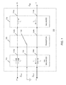
- FIG. 1 illustrates a schematic diagram of an embodiment of a broadband balun.
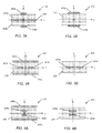
- FIG. 2A and FIG. 2B respectively illustrate cross sections of an example of an unbalanced portion and a balanced portion of the broadband balun shown in FIG. 1 .
- FIG. 3A and FIG. 3B respectively illustrate cross sections of another example of an unbalanced portion and a balanced portion of the broadband balun shown in FIG. 1 .
- FIG. 4A and FIG. 4B respectively illustrate cross sections of yet another example of an unbalanced portion and a balanced portion of the broadband balun shown in FIG. 1 .
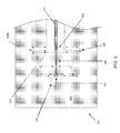
- FIG. 5 illustrates a planar view of an example of a broadband balun with an unbalanced portion including opposing microstrip waveguides.
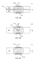
- FIG. 6A through FIG. 6F illustrate respective cross sections of the broadband balun shown in FIG. 5 including example electric field distributions at the respective sections.
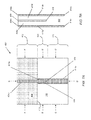
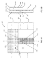
- FIG. 7A and 7B respectively illustrate a planar and a longitudinal cross section of an embodiment of a wideband balun.
- FIG. 8A through FIG. 8C illustrate respective cross sections of the broadband balun shown in FIG. 7A , including example electric field distributions at the various sections identified in FIG. 7A .
- FIG. 9A and 9B respectively illustrate a planar and a longitudinal cross section of another embodiment of a wideband balun.
- FIG. 10A through FIG. 10C illustrate respective cross sections of the broadband balun shown in FIG. 9A , including example electric field distributions at the various sections identified in FIG. 9A .
- FIG. 11A and 11B respectively illustrate a planar and a longitudinal cross section of yet another embodiment of a wideband balun.
- FIG. 12A through FIG. 12F illustrate respective cross sections of the broadband balun shown in FIG. 11A , including example electric field distributions at the various sections identified in FIG. 11A .
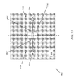
- FIG. 13 illustrates a planar view of an embodiment of two wideband baluns interconnected in a back-to-back configuration, otherwise revered to as a wideband balun choke.
- FIG. 14 illustrates a planar view of an embodiment of a wideband balun circuit including a differential filter.
- FIG. 15 illustrates a schematic view of an embodiment of an integrated circuit including a differential driver and a wideband balun.
- FIG. 16 illustrates a schematic view of another embodiment of an integrated circuit including a differential driver, a wideband balun choke, and a differential receiver.
- FIG. 17 illustrates a flow diagram of a process for coupling differential signals between unbalanced and balanced transmission lines.
- travelling wave structures without elements resonant at any particular frequency, are arranged along a central, longitudinal axis, having in-phase and anti-phase conductive traces configured to collectively support the transfer of differential signals.
- the travelling wave structures can include transmission lines, otherwise referred to as waveguide sections, configured as parallel-plate waveguides, co-planar waveguides, microstrip waveguides and differential stripline waveguides, including parallel-plate and co-planar stripline waveguides.
- the structures are referred to as baluns and can accommodate efficient transfer of differential signals in either direction (e.g., from unbalanced to balanced and from balanced to unbalanced), with minimal reflections or other reductions in signal integrity.
- the baluns include an unbalanced portion having at least one analog or digital ground herein generally referred to as ground.
- the ground is physically isolated (i.e., no direct-current path) from either the in-phase or anti-phase traces. At non-zero frequencies, however, the traces and ground together support common mode signals along the differential signal traces. Such common mode signals are sometimes referred to as even mode signals.
- the at least one analog ground is substantially removed, or otherwise isolated from the differential signal traces in the balanced portion. The transition from ground to no-ground occurs in the transition region. Consequently, common mode signals are no longer supported along the balanced portion as an effective common mode impedance measured between either trace and the at least one analog ground approaches an open circuit (i.e., infinite impedance).
- the differential signal traces however, remain capable of supporting differential mode propagation. Such differential mode signals without common mode signals represents a balanced configuration.
- FIG. 1 A schematic diagram of an embodiment of a broadband, differential-signal balun 100 is illustrated in FIG. 1 .
- the balun 100 includes an unbalanced portion 102 having an in-phase signal trace 104a, an anti-phase signal trace 104b, and at least one analog ground 106.
- the in-phase 104a trace, the anti-phase 104b trace and the at least one ground 106 are collectively configured to support at least one propagating waveguide mode.
- a first waveguide may include the in-phase trace 104a and the analog ground 106, having a first characteristic impedance Z OU1 .
- a second waveguide may include the anti-phase trace 104b and the analog ground 106, having a second characteristic impedance Z OU2 .
- the unbalanced portion 102 can be considered unbalanced at least in that the currents on either the in-phase or anti-phase traces 104a, 104b interact with the analog ground 106.
- the unbalanced portion 102 is capable of supporting oppositely directed currents, sometimes referred to as differential mode, on the in-phase and anti-phase traces 104a, 104b (i.e., I o + , I o - ), having a respective odd mode impedance with respect to each other.
- the unbalanced portion 102 is capable of supporting co-aligned currents, sometimes referred to as a common mode, on the in-phase and anti-phase traces 104a, 104b (i.e., I e + , I e - ), having an even mode impedance with respect to the analog ground 106.
- the balun 100 also includes a balanced portion 112 having an in-phase signal trace 114a and an anti-phase signal trace 114b, without any analog ground reference.
- the in-phase 114a trace and the anti-phase 114b trace are arranged as a balanced waveguide capable of supporting a balanced propagating waveguide mode.
- the balanced waveguide is formed by the traces 114a, 114b, having a respective characteristic impedance Z OB .
- the in-phase signal trace 114a is in electrical communication with the in-phase trace 104a of the unbalanced portion 102.
- the anti-phase signal trace 114b is in electrical communication with the anti-phase trace 104b of the unbalanced portion 102.
- the structure can be considered balanced at least in that the currents on either the in-phase or anti-phase traces 104a, 104b are substantially equal and opposite (i.e., I o + , I o - ).
- the aligned currents on the in-phase and anti-phase traces 104a, 104b i.e., I e + , I e - ), having an even mode impedance with respect to the analog ground 106.
- the balun 100 also includes a transition region 120 having an in-phase signal trace 124a and an anti-phase signal trace 124b.
- the in-phase 124a trace and the anti-phase 124b trace are arranged as a waveguide capable of supporting a propagating waveguide mode.
- the in-phase signal trace 124a is in electrical communication between the in-phase trace 104a of the unbalanced portion 102 and the in-phase trace 114a of the balanced portion 112.
- the anti-phase signal trace 124b is in electrical communication between the in-phase trace 104b of the unbalanced portion 102 and the in-phase trace 114b of the balanced portion 112.
- the transition region 120 also includes a partial analog ground 126 in electrical communication with the analog ground 106 of the unbalanced portion 102.
- the unbalanced portion 202 includes an in-phase trace 204a, an anti-phase trace 204b and an analog ground 206.
- the analog ground 206 is provided as a ground plane 206.
- An upper dielectric layer 208a abuts a top surface of the analog ground plane 206 and a lower dielectric layer 208b abuts a bottom surface of the ground plane 206.
- the in-phase trace 204a extends along a top surface if an upper dielectric layer 208a, opposite the top surface of the analog ground plane 206.
- the anti-phase trace 204b extends along a bottom surface of the lower dielectric layer 208b, opposite the bottom surface of the analog ground plane 206.
- the in-phase and anti-phase traces 204a, 204b are substantially uniform in cross section, extending parallel to a central, longitudinal axis.
- FIG. 2B A cross section of an example of a balanced portion 212 of the broadband balun 100 is shown in FIG. 2B .
- the balanced portion 212 corresponds to a balun having an unbalanced portion 202 as shown in FIG. 2A .
- the balanced portion 212 includes an in-phase trace 214a and an anti-phase trace 214b.
- a planar dielectric layer 208 extends between the in-phase trace 214a and the anti-phase trace 214b, with in-phase trace 204a extending along a top surface of the dielectric layer 208, and the anti-phase trace 204b extending along a bottom surface of the dielectric layer 208 and without the analog ground plane 206.
- the in-phase and anti-phase traces 214a, 214b are substantially uniform in cross section extending parallel to the central, longitudinal axis of the balun 100.
- the in-phase trace 204a, the upper dielectric layer 208a and the ground plane 206 represent a first microstrip waveguide.
- the first microstrip waveguide can be driven by an in-phase portion of a differential signal (not shown).
- the anti-phase trace 204b, the lower dielectric layer 208b and the ground plane 206 also represent a second microstrip waveguide.
- the second microstrip waveguide can be driven by an anti-phase portion of the differential signal.
- Reference x and y coordinate axes are illustrated for each of the transverse cross-sections, having an origin coincident with the central, longitudinal axis of the balun 100.
- Each of the traces 204a, 204b has a respective width (w U ), measured along the x-axis, a thickness (t U ) measured along the y-axis and a height (h U ) above the ground plane 206 also measured along the y-axis.
- the first and second microstrip waveguides have respective characteristic impedances Z OU1 , Z OU2 , each of which that can be determined through techniques known to those skilled in the art of waveguide design, according to respective dimensions w U , t U , h U and a dielectric constant ( ⁇ r ) of the dielectric layer 208. It is apparent that the unbalanced portion 202 exhibits a high degree of symmetry, being symmetric with respect to each of the x and y axes, described herein as being symmetric with respect to the central, longitudinal axis.
- the in phase trace 214a and the anti-phase trace 214b represent a parallel plate waveguide.
- the traces 214a, 214b have respective widths (w B ), measured along the x-axis, thicknesses (t B ) measured along the y-axis and height (h B ) with respect to each other also measured along the y-axis.
- the parallel plate waveguide has a respective characteristic impedance Z OB , which can also be determined through generally known techniques according to respective dimensions w B , t B , h B and a dielectric constant ( ⁇ r ) of the dielectric layer 208. It is apparent that the balanced portion 212 also exhibits a high degree of symmetry, being symmetric with respect to each of the x and y axes (i.e., symmetric with respect to the central, longitudinal axis).
- FIG. 3A A cross section of another example of an unbalanced portion 222 of the broadband balun 100 is shown in FIG. 3A .
- the unbalanced portion 222 includes an in-phase trace 224a and an anti-phase trace 224b extending along a longitudinal axis of the balun 100, between an upper analog ground 226a and a lower analog ground plane 226b.
- a dielectric layer 228 extends between the upper and lower analog ground plane layers 226a, 226b, with the in-phase and anti-phase traces 224a, 224b embedded within a dielectric layer 228.
- the in-phase and anti-phase traces 224a, 224b (generally 224) are substantially uniform in cross section extending parallel to the longitudinal axis. It is envisioned that the dielectric layer may include multiple layers, for example two layers, one above and one below the traces 224.
- FIG. 3B A cross section of another example of a balanced portion 232 of the broadband balun 100 is shown in FIG. 3B .
- the balanced portion 232 corresponds to a balun having an unbalanced portion 222 as shown in FIG. 3A .
- the balanced portion 232 includes an in-phase trace 234a and an anti-phase trace 234b embedded within the planar dielectric layer 228 and without either of the upper or lower analog ground planes 226a, 226b.
- the in-phase and anti-phase traces 234a, 234b are substantially uniform in cross section extending parallel to the longitudinal axis of the balun 100.
- the in-phase trace 224a, the anti-phase trace 224b and the upper and lower ground planes 226a, 226b represent a co-planar, stripline waveguide.
- the in-phase trace 224a, the anti-phase trace 224b can be driven by a differential signal source (not shown).
- Reference x and y coordinate axes are illustrated for the transverse cross-section, having an origin coincident with the longitudinal axis of the balun 100.
- Each of the traces 224a, 224b has a respective width (w U ) and spacing (s U ), measured along the x-axis, a thickness (t U ) measured along the y-axis and a uniform height (h U ) with respect to either ground plane 226a, 226b also measured along the y-axis.
- the co-planar, stripline waveguide has a characteristic impedances Z OU , which can be determined according to respective dimensions w U , s U , t U , h U and a dielectric constant ( ⁇ r ) of the dielectric layer 228. It is apparent that the unbalanced portion 222 exhibits a high degree of symmetry, being symmetric with respect to each of the x and y axes.
- the in phase trace 234a and the anti-phase trace 234b represent a co-planar waveguide.
- the traces 234a, 234b have respective widths (w B ) and spacing (s U ), measured along the x-axis, and thicknesses (t B ) measured along the y-axis.
- the a co-planar waveguide has a respective characteristic impedances Z OB , which can also be determined according to respective dimensions w B , t B and a dielectric constant ( ⁇ r ) of the dielectric layer 228. It is apparent that the balanced portion 232 also exhibits a high degree of symmetry, being symmetric with respect to each of the x and y axes.
- FIG. 4A A cross section of yet another example of an unbalanced portion 242 of the broadband balun 100 is shown in FIG. 4A .
- the unbalanced portion 242 includes an in-phase trace 244a and an anti-phase trace 244b extending along a longitudinal axis of the balun 100, between upper and lower analog ground planes 246a , 246b.
- a dielectric layer 248 extends between the upper and lower analog ground planes 246a, 246b, with the in-phase and anti-phase traces 244a, 244b embedded within the dielectric layer 248.
- the in-phase and anti-phase traces 244a, 244b are substantially uniform in cross section extending parallel to a longitudinal axis.
- the dielectric layer may be formed as multiple layers, for example two layers, one above, one below, and perhaps one between the traces 244. In at least some embodiments a homogeneous dielectric extends above 246a and below 246b (not shown).
- FIG. 4B A cross section of yet another example of a balanced portion 252 of the broadband balun 100 is shown in FIG. 4B .
- the balanced portion 252 corresponds to a balun having an unbalanced portion 242 as shown in FIG. 4A .
- the balanced portion 252 includes an in-phase trace 254a and an anti-phase trace 254b embedded within the planar dielectric layer 248 and without either of the upper or lower analog ground planes 246a, 246b.
- the in-phase and anti-phase traces 254a, 254b are substantially uniform in cross section extending parallel to a longitudinal axis.
- the in-phase trace 244a, the anti-phase trace 244b and the upper and lower ground planes 246a, 246b represent a parallel-plate, stripline waveguide.
- the in-phase trace 244a, the anti-phase trace 244b can be driven by a differential signal source (not shown).
- Reference x and y coordinate axes are illustrated for the transverse cross-section, having an origin coincident with the longitudinal axis of the balun 100.
- Each of the traces 244a, 244b has a respective width (w U ), measured along the x-axis, a thickness (t U ) and spacing (s U ), measured along the y-axis and a uniform height (h U ) with respect to each other measured along the y-axis.
- the parallel-plate, stripline waveguide has a characteristic impedances Z OU , which can be determined according to respective dimensions w U , (s U ), t U , h U and a dielectric constant ( ⁇ r ) of the dielectric layer 248. It is apparent that the unbalanced portion 242 exhibits a high degree of symmetry, being symmetric with respect to each of the x and y axes.
- the traces 244a and 244b are offset from each other in the x direction (plus and minus) for setting Z OU without having to adjust the spacing s U or heights h U (not shown).
- the in phase trace 254a and the anti-phase trace 254b represent a parallel-plate waveguide, embedded within the dielectric layer 248.
- the traces 254a, 254b have respective widths (w B ) and spacing (s B )" measured along the x-axis, a thicknesses (t B ) and a separation (h B ) measured along the y-axis.
- the parallel-plate waveguide has a respective characteristic impedances Z OB , which can also be determined according to respective dimensions w B , t B , h B and a dielectric constant ( ⁇ r ) of the dielectric layer 248. It is apparent that the balanced portion 252 also exhibits a high degree of symmetry, being symmetric with respect to each of the x and y axes.
- FIG. 5 illustrates a planar view of an example of a broadband balun 300 with an unbalanced portion 302 including opposing microstrip waveguides, for example, similar to those illustrated in FIG. 2A .
- An in-phase trace is visible above an upper dielectric layer 308a.
- Also shown as a shaded region is a top surface of a central ground plane 306, visible through the dielectric layer, which has been illustrated as translucent for this purpose.
- a balanced portion 312 is formed by removal of a portion of the ground plane 306 from between the in-phase and anti-phase traces.
- a perimeter of a ground plane aperture 314 is illustrated as a dashed line, indicating that it lies within the dielectric layer 308.
- ground plane 306 it is not necessary that the entire ground plane 306 be removed within the balanced portion 312. Rather, the ground plane 308 is removed from between the parallel traces, the removal extending for some distance away from the traces, such that electromagnetic coupling to the ground plane (e.g., by way of a capacitance) is substantially negligible at a distance of at least 10 s B .
- a minimum separation between ground plane and traces is at least, e.g., 10 s B .
- a transition layer 320 is provided between the unbalanced portion 302 and the balanced portion 312. Also shown is a "footprint" 325 for a differential circuit as may be coupled to the balun 300.
- a differential signal interface 330 is provided within the vicinity of differential circuit footprint 325 and adapted for coupling to contacts of the differential circuit portrayed by its footprint 325.
- the differential circuit may be a signal source, for example including a differential driver, or a signal sink, for example including a differential receiver.
- signals may flow in either direction along the wideband balun 300, from the unbalanced portion to the balanced portion, and visa versa.
- another differential circuit (not shown) can be coupled to an end of the balanced portion 312 opposite the transition region 320.
- FIG. 6A through FIG. 6F illustrate respective cross sections of the broadband balun 300 shown in FIG. 5 including example electric field distributions at the various sections identified in FIG. 5 .
- an in-phase terminal 334a is located on a top surface of an upper dielectric layer 308a.
- the in-phase terminal 334a is in electrical communication with an in-phase trace 304a of the unbalanced portion 302 through a first conductive (e.g., plated-through) via 335a.
- the anti-phase terminal 334a is in electrical communication with an anti-phase trace 304b through a second conductive via 335b.
- a ground plane 306 is provided between the two traces 304a, 304b.
- An aperture is provided within the ground plane 306 to allow the second via 335b to pass through to an opposite side of the ground plane 306, while remaining isolated from the ground plane 306.
- Also shown are indications of a differential electric field distribution resulting from the presence of a differential signal on the traces 304a, 304b.
- the traces 304a, 304b are vertically misaligned to accommodate intersection with their respective vias 335a, 335b.
- an upper electric field distribution between the in-phase trace 304a and a top surface of the ground plane 306 is substantially aligned with a lower electric field distribution between the anti-phase trace 304b and a bottom surface of the ground plane 306.
- FIG. 6D a portion of the transition region 320 is shown in a fourth section taken along D-D'.
- the ground plane 306 is substantially removed, except for a portion of a ground plane extension.
- the ground plane extension is in vertical alignment and substantially equidistant between the in-phase and anti-phase traces 304a, 304b. At least some of the electric field lines terminate at the ground plane 306, while others in the outer regions extend substantially uninterrupted between the traces 304a, 304b extending around the outer lateral extent of the ground plane extension.
- FIG. 6E another portion of the transition region 320 is shown in a fifth section taken along E-E'.
- FIG. 6F a sixth section taken along F-F', a cross section of the balanced portion 312 is shown. More particularly, no portion of the ground plane 306 exists, extension or otherwise, within the vicinity of the traces 314a, 314b.
- the electric field distributions of the unbalanced portion with the ground plane 306 are substantially the same as the electric field distributions of the balanced portion without the ground plane 306.
- the balun 300 By removal of the ground plane, the balun 300 is effective in removing common mode currents between the traces 304a, 304b and the ground plane 306. By removal of the ground plane, the even mode currents effectively vanish (i.e., the even mode impedance approaches infinity), while the odd mode currents prevail.
- the balun 300 By relying on travelling wave structures (e.g., waveguides), without any resonant elements, the balun 300 performs well over a wide bandwidth. By providing a smooth transition of electric field distributions, the balun 300 avoids unwanted reflections, again supporting wideband operation. By providing impedance matching between the unbalanced and balanced portions, the balun 300 further avoids unwanted reflections supporting wideband operation.
- FIG. 7A and 7B respectively illustrate planar and longitudinal cross section taken along D-D' of an embodiment of a wideband balun 400'.
- Balun 400' shows details of the balun in circuit 300 of FIG. 5 and is shown as Quasi-TEM instead TEM since the dielectric 408 is shown as bounded by grounds 404a and 404b instead of homogeneous dielectric shown in FIG. 6 B through 6F extending substantially above 304a and below 304b.
- the balun 400' includes an unbalanced portion 402, a transition region 420 and a balanced portion 412.
- the unbalanced region 402 includes a vertically aligned pair of opposing microstrip waveguides formed along opposite sides of a central ground plane 406 (again, the ground plane is illustrated as shaded, being visible through a dielectric layer).
- a first microstrip waveguide includes an in-phase conductive trace 404a and a second microstrip waveguide includes a parallel anti-phase conductive trace 404b.
- Each trace 404a, 404b is separated from a respective side of the conductive ground plane 406 by a dielectric layer 408a, 408b (generally 408).
- the balanced region 412 includes a single, parallel-plate waveguide.
- the parallel-plate waveguide includes an in-phase conductive trace 414a and a parallel anti-phase conductive trace 414b, separated by a dielectric 408 layer, without the conductive ground plane 406.
- the transition region 420 includes a bounding edge 413 of the ground plane 406. In the illustrative example, the edge is substantially perpendicular to a longitudinal axis of the balun 400', parallel to and centrally aligned between the pairs of conductive traces 404a-404b, 414a-414b.
- the transition region 420 also includes an extension 416 projecting away from the bounding edge 413.
- the extension 416 projects toward the balanced portion 412.
- the extension 416 is generally symmetric about a plane bisecting the traces 404a-404b, 414a-414b.
- the extension 416 can include a taper, for example, being substantially wider at an end adjacent to the bounding edge 413, and narrowing along its projection toward a terminal end 418.
- the taper can be linear, such as the triangular taper shown.
- the extension 416 can include a curved taper or a combination of linear and curved tapers.
- the extension 416 including any taper will assist in transitioning or otherwise shaping a transverse electric field distribution along the axial length of the transition region 420 between respective transverse electric field distributions of the unbalanced portion 402 and the balanced portion 412.
- the width of trace 404a is transitioned to the wider trace of 414a at 415.
- 404b is transitioned to the width of 414b at 415.
- a width of the traces 404a, 404b of the unbalanced portion 402 is different than a width of the traces 414a, 414b of the balanced portion 412.
- the traces of the balanced portion 412 can be wider than the traces of the unbalanced portion.
- a separate between the traces can also differ between the unbalanced and balanced regions 402, 412. Selection of such physical parameters as the widths, heights or separation spacing, thicknesses and dielectric constant can be selected to control a physical property of a respective waveguide, such as its characteristic impedance.
- the physical parameters of the microstrip waveguides of the unbalanced portion 402 can be selected for a characteristic impedance of about 50 Ohms.
- the physical parameters of the parallel-plate waveguide of the balanced portion 420 can be selected for a characteristic impedance of about 100 Ohms.
- characteristic impedances of the unbalanced portion 402 and balanced portion 412 are such that the possibility of any unwanted reflections or mismatch to electromagnetic waves propagating along the balun 400' are minimized.
- Unwanted reflections can be characterized according to such parameters as a reflection coefficient (e.g., a ratio of a reflected wave voltage to an incident wave voltage) or as another parameter generally known as a voltage standing wave ratio (VSWR).
- a reflection coefficient e.g., a ratio of a reflected wave voltage to an incident wave voltage
- VSWR voltage standing wave ratio
- Another value known as the return loss can be determined as an estimate of inefficiency of energy transfer along the balun, for example, due to unwanted reflections.
- the balun 400' exhibits favorable performance (e.g., reflection coefficient, VSWR, return loss) over a relatively wide range of operating frequencies.
- Such measures of favorable performance may include a VSWR of less than about 2:1, or a return loss of greater than about -9.54 dB.
- wideband includes operating frequency range of at least ten times its lower frequency (i.e., 10:1).
- the balun 400' is capable of operation over at least one of frequency band of operation generally known as millimeter wave transmission and microwave transmission.
- FIG. 8A through FIG. 8C illustrate respective cross sections of the broadband balun 400' shown in FIG. 7A , including example transverse electric fields at the various sections identified in FIG. 7A .
- a first section taken along A-A' of the unbalanced portion 402 illustrated in FIG. 8A shows transverse electric field distribution with electric fields directed from the in-phase trace 404a towards the ground plane 406.
- the electric field distribution necessarily satisfies electromagnetic boundary conditions of the structure, effectively behaving as if a mirror-image trace having an opposite potential was located along an opposite side of the ground plane.
- the of transverse electric field distribution with electric fields directed from the anti-phase trace 404b towards the ground plane 406 also satisfies boundary conditions of the structure, effectively behaving as if a mirror-image trace having an opposite potential was located along an opposite side of the ground plane.
- boundary conditions correspond the actual construction of the in-phase and anti-phase traces 404a, 404b
- the transverse electric field distributions of the unbalanced portion are substantially aligned with the ground plane 406, which extends along an equipotential plane.
- waveguide modes supported in each of the unbalanced and balanced portions 402, 412 are Quasi transverse electromagnetic mode (Quasi-TEM). Accordingly, the longitudinal electric field components do exist to a lesser degree than the transverse electromagnetic mode which is more substantial
- a second section taken along B-B' of the transition region 420 illustrated in FIG. 8B shows the ground plane extension 418 disposed between the traces 404a, 404b. Outer fields, those most removed from the y-axis, extend substantially unbroken from the in-phase trace 404a, terminating on the anti-phase trace 404b. Inner fields from each trace 404a, 404b, those closer to the y-axis, intersect and therefore terminate along the ground plane extension 418.
- a third section taken along C-C' of the balanced region 412 illustrated in FIG. 8C shows the parallel-plate waveguide formed by the in-phase trace 414a and the anti-phase trace 414b. Electric fields extend substantially unbroken from the in-phase trace 414a, terminating on the anti-phase trace 414b. Electric field distributions of the unbalanced and balanced portions are substantially identical, but for the presence of the ground plane 406.
- FIG. 9A and 9B respectively illustrate planar and longitudinal cross section taken along D-D' of another embodiment of a wideband balun 400".
- the balun 400" includes an unbalanced portion 422, a transition region 440 and a balanced portion 432.
- the unbalanced region 422 includes a coplanar stripline waveguide formed between upper and lower parallel ground planes 426a, 426b.
- the waveguide includes an in-phase conductive trace 424a and a co-planar, parallel anti-phase conductive trace 424b.
- Each trace 424a, 424b is separated from upper and lower adj acent ground planes 426a, 426b by an interposed dielectric layer 428a, 428b (generally 428).
- the balanced region 432 includes a co-planar waveguide embedded within the dielectric layer 428.
- the co-planar waveguide includes an in-phase conductive trace 434a and a parallel anti-phase conductive trace 434b.
- the transition region 440 includes an upper bounding edge 433a of the upper ground plane 426a and a lower bounding edge 433b of the lower ground plane 426b.
- the edges 433a, 433b are substantially perpendicular to a longitudinal axis of the balun 400", parallel to and centrally aligned between the pairs of conductive traces 424a, 424b, 434a, 434b.
- the edges 433a, 433b are substantially aligned or otherwise overlapping in a common transverse plane.
- the transition region 440 also includes an upper extension 436a projecting away from the upper bounding edge 433a and a lower extension 436b projecting away from the lower bounding edge 433b.
- the extensions 436a, 436b project toward the balanced portion 432.
- the extensions 436a, 436b are generally symmetric about a plane bisecting the traces 424a, 424b, 434a, 434b and including the longitudinal axis.
- the extensions 436a, 436b can include a taper, for example, being substantially wider at an end adjacent to the bounding edge 433a, 433b, narrowing along its projection to a terminal end 438a, 438b.
- the taper can be linear, such as the triangular taper shown.
- the extensions 436a, 436b can include a curved taper or a combination of linear and curved tapers.
- the extensions 436a, 436b including any taper will assist in transitioning or otherwise shaping an electric field along the transition region 440 between respective transverse electric field distributions of the unbalanced portion 422 and the balanced portion 432.
- a width of the traces 424a, 424b of the unbalanced portion 422 is different than a width of the traces 434a, 434b of the balanced portion 432.
- the traces of the balanced portion 432 can be wider than the traces of the unbalanced portion 422.
- Transition between different widths can include a stepped discontinuity, a chamfer 435 as shown, or any other suitable profile. In some embodiments, the transition can be accomplished in multiple such steps.
- a separate between the traces can also differ between the unbalanced and balanced regions 422, 432.
- Selection of such physical parameters as the widths, heights or separation spacing, thicknesses and dielectric constant can be selected to control a physical property of a respective waveguide, such as its characteristic impedance.
- the physical parameters of the microstrip waveguides of the unbalanced portion 422 can be selected for a characteristic impedance of about 50 Ohms.
- the physical parameters of the co-planar waveguide of the balanced portion 432 can be selected for a characteristic impedance of typically about 50 Ohms to 200 Ohms.
- characteristic impedances of the unbalanced portion 422 and balanced portion 432 are chosen such that the possibility of unwanted reflections or mismatch to electromagnetic waves propagating along the balun 400" are minimized.
- FIG. 10A through FIG. 10C illustrate respective cross sections of the broadband balun shown in FIG. 9A , including example transverse electric fields at the various sections identified in FIG. 9A .
- a first section taken along A-A' of the unbalanced portion 422 is illustrated in FIG. 10A , showing transverse electric field distribution with electric fields directed from each of the in-phase and anti-phase traces 424a, 424b towards the opposing trace and towards the ground planes 426a, 426b.
- the electric field distribution may partially extend above and below the dielectric 428 (not as shown) for Quasi-TEM (as shown in FIG.
- a second section taken along B-B' of the transition region 440 is illustrated in FIG. 10B , showing the upper and lower ground plane extensions 436a, 436b disposed respectively above and below the traces 424a, 424b.
- a narrowing of the ground planes along the extensions 436a, 436b alters the fields according to electromagnetic boundary conditions of the reduced extent ground. The net effect in the illustrative example is to effectively bend the outer electric fields of each of the traces 424a, 424b toward the opposite trace (i.e., toward the y-axis).
- a third section taken along C-C' of the balanced region 432 is illustrated in FIG. 10C , showing the co-planar waveguide formed by the in-phase trace 434a and the anti-phase trace 434b.
- Electric fields extend substantially unbroken from the in-phase trace 434a, terminating on the anti-phase trace 434b.
- the series of cross sections illustrates how the tapered extension smoothly transitions transverse electric fields from the unbalanced portion 422 to the balanced portion 432 over a distance along the longitudinal axis.
- FIG. 11A and 11B respectively illustrate planar and longitudinal cross section taken along D-D' of another embodiment of a wideband balun 400"'.
- the balun 400"' includes an unbalanced portion 442, a transition region 460 and a balanced portion 452.
- the unbalanced region 442 includes a parallel-plate stripline waveguide formed between upper and lower parallel ground planes 446a, 446b.
- the waveguide includes an in-phase conductive trace 444a and a vertically aligned parallel anti-phase conductive trace 444b.
- Each trace 444a, 444b is separated from each other and from adjacent ground planes 446a, 446b by a dielectric layer 448.
- the balanced region 452 includes a parallel-plate waveguide embedded within the dielectric layer 448.
- the parallel-plate waveguide includes an in-phase conductive trace 454a and a parallel anti-phase conductive trace 454b.
- the transition region 460 includes an upper bounding edge 453a of the upper ground plane 446a and a lower bounding edge 453b of the lower ground plane 446b.
- the edges 453a, 453b are substantially perpendicular to a longitudinal axis of the traces 444a, 444b, 454a, 454b.
- the edges 453a, 453b are substantially aligned or otherwise overlapping in a common transverse plane.
- the transition region 460 also includes an upper extension 456a projecting away from the upper bounding edge 453a and a lower extension 456b projecting away from the lower bounding edge 453b.
- the extensions 456a, 456b project toward the unbalanced portion 442.
- the extensions 436a, 436b are generally symmetric about a plane bisecting the traces 444a, 444b, 454a, 454b and including the longitudinal axis.
- the extensions 456a, 456b can include a taper, for example, being substantially wider at an end adjacent to the bounding edge 453a, 453b, narrowing along its projection to a terminal end 458a, 458b.
- the extension is provide as a notch in the ground plane 466a, 466b.
- the taper can be linear, such as the triangular taper shown.
- the extensions 456a, 456b can include a curved taper or a combination of linear and curved tapers.
- the extensions 456a, 456b including any taper will assist in transitioning or otherwise shaping transverse electric fields along the transition region 460 between respective transverse electric field distributions of the unbalanced portion 442 and the balanced portion 452.
- the wideband balun 400"' further includes a split intermediate analog ground plane including a left-hand portion 466a and a right-hand portion 466b.
- each of the left and right-hand portions 466a, 466b of the intermediate analog ground plane resides in the same plane substantially equidistant between the upper and lower ground planes 446a, 446b and along either side of a plane bisecting the traces 444a, 444b, 464a, 464b and including the longitudinal axis.
- the left-hand intermediate ground plane 466a includes a respective bounding edge 463a.
- the right-hand intermediate ground plane 466b includes a respective bounding edge 463b.
- the edges 463a, 463b are substantially aligned along a common axial location and perpendicular to a longitudinal axis of the traces 444a, 444b, 454a, 454b. In the illustrative example, the edges 463a, 463b extend beyond the bounding edge 453a, 453b of the upper and lower ground planes 446a, 446b, closer to the balanced portion 452.
- edges 463a, 463b, 453a, 453b can be arranged in overlapping arrangement at a common axial location, or that the upper and lower edges 453a, 453b can extend further towards the balanced portion 452 than the intermediate edges 463a, 463b. It is also envisioned that in some embodiments that the vias 469a and 469b extend further towards the balanced portion 452 than the intermediate edges 463a, 463b.
- the left and right-hand portions 466a, 466b of the intermediate ground plane are spaced sufficiently apart from the in-phase and anti-phase traces 444a, 444b of the unbalanced portion 442 such that coupling of transverse electric fields to the intermediate ground plane is substantially negligible within the unbalanced region 442.
- the left and right-hand portions 466a, 466b of the intermediate ground plane are spaced relatively close to the in-phase and anti-phase traces 464a, 464b of the intermediate region 460 resulting in coupling of at least a portion of the transverse electric fields to the intermediate ground plane.
- the balun 400"' further includes left and right-hand vertical analog ground screens 469a, 469b.
- Such vertical ground screens 469a, 469b can be provided, for example, by vertically aligned conductive elements.
- the vertical conductive elements are provided by conducting (i.e., plated-through) vias extending between and electrically interconnecting the upper and lower ground planes 446a, 446b.
- the conductive vias are disposed adjacent to edges of the left and right-hand portions 466a, 466b facing the central axis.
- Spacing between adjacent vias of such a "picket fence" arrangement can be controlled, for example, having a maximum separation between adjacent vias of less than one-quarter minimum-operating wavelength. Preferably, separation between adjacent vias is no more than about one-tenth of a minimum-operating wavelength.
- a width of the traces 444a, 444b of the unbalanced portion 442 is the same as a width of the traces 454a, 454b of the balanced portion 452. In other embodiments the widths are different, as illustrated.
- the traces of the balanced portion 452 can be narrower or wider (as shown) than the traces of the unbalanced portion 442.
- a separate between the traces 444a-444b, 454a-454b can also differ or be the same (as shown) between the unbalanced and balanced regions 442, 452.
- the physical parameters of the parallel-plate stripline waveguide of the unbalanced portion 442 can be selected for a characteristic impedance of typically about 50 Ohms to 100 Ohms.
- the physical parameters of the embedded parallel-plate waveguide of the balanced portion 452 can be selected for a preferred characteristic impedance, for example, of about 50 Ohms to 100 Ohms.
- characteristic impedances of the unbalanced portion 442 and balanced portion 452 are chosen such that the possibility of unwanted reflections or mismatch to electromagnetic waves propagating along the balun 400"' are minimized.
- transitions between traces having different widths can be accomplished in a stepped or graded fashion (e.g., a rectangular transition from one width to the next).
- transitions between different widths can be accomplished in a less abrupt manner, for example having a taper or chamfer as provided in the examples described herein.
- the taper can be linear, curved, or any suitable combination of linear and curved.
- the transition can be accomplished in multiple transitions occurring over a series of steps.
- intermediate traces 464a, 464b are provided in the transition region 460, having a width between the widths of the unbalanced portion traces 444a, 444b and the balanced portion traces 454a, 454b.
- FIG. 12A through FIG. 12F illustrate respective cross sections of the broadband balun shown in FIG. 11A , including example transverse electric fields at the various sections identified in FIG. 11A .
- a first section taken along A-A' of the unbalanced portion 422 illustrated in FIG. 12A shows transverse electric field distribution including electric fields directed from the in-phase and anti-phase traces 444a, 444b towards the opposing trace and towards the upper and lower ground planes 466a, 466b.
- the electric field distribution satisfies boundary conditions of the structure, effectively behaving as if a first symmetric image parallel-plate waveguide having an opposite potential was located along an opposite side of the upper ground plane 466a and a second symmetric image parallel-plate waveguide having an opposite potential was located along an opposite side of the lower ground plane 466b (i.e., mirror images).
- a second section taken along B-B' of the transition region 460 illustrated in FIG. 12B shows the upper and lower ground plane extensions 446a, 446b disposed respectively above and below the traces 444a, 444b.
- a central opening in each of the ground planes 446a, 446b along the extensions 456a, 456b alters the fields according to electromagnetic boundary conditions of the altered ground.
- the net result in the illustrative example is to effectively bend the upper and lower electric fields nearest the y-axis of each of the traces 444a, 444b outward (i.e., away from the y-axis).
- This arrangement begins reshaping of the fields between the traces and their adjacent ground plane extension 446a, 446b from vertical (i.e., y-axis directed) toward horizontal (i.e., x-axis directed).
- a third section taken along C-C' of the balanced region 452 illustrated in FIG. 12C shows an increased central opening in each of the ground planes 446a, 446b along the extensions 456a, 456b further altering or otherwise shaping the transverse electric fields according to electromagnetic boundary conditions of the altered grounds 446a, 446b.
- the net effect in the illustrative example is to effectively bend the upper and lower electric fields further away from the y-axis.
- the left and right-hand portions 466a, 466b of the intermediate ground plane and the corresponding vertical ground screens 469 are arranged relatively close to the in-phase and anti-phase traces 464a, 464b of the transition region 460.
- the proximity is such that at least a portion of the transverse electric field distribution satisfies boundary conditions of the structure, effectively behaving as if a first symmetric image parallel-plate waveguide having an opposite potential was located along an opposite side of the left and right vertical ground screens 469a, 469b.
- the result is to reshape those fields further away from the plane bisecting the traces and including the longitudinal axis from vertical (i.e., y-axis directed) toward horizontal (i.e., x-axis directed).
- a fourth section taken along D-D' of the balanced region 452 illustrated in FIG. 12D shows an even further increased central opening in each of the ground planes 446a, 446b along widening extensions further altering or otherwise shaping the transverse electric fields according to electromagnetic boundary conditions of the altered grounds 446a, 446b.
- the left and right-hand portions 466a, 466b of the intermediate ground plane remain relatively close to the in-phase and anti-phase traces 464a, 464b of the transition region 460, whereas the corresponding vertical ground screens 469a, 469b have been moved farther away from the traces 464a, 464b.
- the proximity is such that at least a portion of the transverse electric field distribution satisfies boundary conditions of the structure, effectively behaving as if a first symmetric image parallel-plate waveguide having an opposite potential was located along an opposite side of the left and right vertical ground screens 469a, 469b.
- the result is to further reshape those fields further away from the plane bisecting the traces and including the longitudinal axis from vertical (i.e., y-axis directed) toward horizontal (i.e., x-axis directed).
- a fifth section taken along E-E' of the balanced region 452 illustrated in FIG. 12E shows the embedded parallel-plate waveguide after removal of the upper and lower ground planes 446a, 446b (e.g., axially located between the bounding edge 453 and the balanced portion 452).
- the transverse electric fields adjust according to electromagnetic boundary conditions of the altered ground having left and right-hand portions 466a, 466b of the intermediate ground plane disposed along an equipotential plane.
- the transverse electric fields have been coerced or otherwise tailored from an unbalanced region distribution of the parallel-plate stripline waveguide to a balanced region distribution of the embedded parallel-plate waveguide by imposing boundary conditions of one or more of the upper and lower ground planes 446a, 446b, the left and right-hand portions 466a, 466b of the intermediate ground plane and the left and right-hand vertical ground screens 469a, 469b.
- a sixth section taken along F-F' of the balanced region 452 illustrated in FIG. 12F shows the embedded parallel-plate waveguide formed by the in-phase trace 454a and the anti-phase trace 454b. Electric fields extend substantially unbroken from the in-phase trace 454a, terminating on the anti-phase trace 454b.
- the series of cross sections illustrates how the tapered extension smoothly transitions transverse electric fields from the unbalanced portion 442 to the balanced portion 452.
- FIG. 13 illustrates a planar view of an embodiment of a balun circuit including two wideband baluns 510a, 510b interconnected in a back-to-back configuration, otherwise revered to as a wideband balun choke 500.
- a first balun 510a includes a differential signal port 530a disposed at an unbalanced end of the balun 510a.
- a second balun 510b includes a differential signal port 530b disposed at an unbalanced end of the balun 510b.
- An analog ground 506 includes an aperture 514 in the vicinity of the balanced portions of the adjoined baluns 510a, 510b.
- Each of the baluns 510a, 510b is arranged along a common longitudinal axis and in facing arrangement of their respective balanced ends.
- the balanced ends are coupled or otherwise adjoined allowing for signal propagation from one differential signal port 530a, 530b to the other 530b, 530a.
- the baluns 510a, 510b can be any suitable broadband balun, such as those described herein.
- the baluns 510a, 510b share a common configuration.
- FIG. 14 illustrates a planar view of an embodiment of another balun circuit 550 including a wideband balun 560 combined with a differential filter 585.
- a wideband balun 560 includes a differential signal port 580 disposed at one end of an unbalanced portion 562 of the balun 560. Also shown is a footprint 575 of a differential circuit element for interconnection to the differential signal port 580.
- the differential circuit may be a differential signal source (e.g., driver) or sink (e.g., receiver).
- the balun 560 includes a balanced portion 572 and a transition region according to the techniques described herein.
- An analog ground 556 includes an aperture 564 in the vicinity of the balanced portion 572 and at least a balanced end of the filter 585.
- a differential signal is provided at one end of the balun 560, for example, at the unbalanced portion 562 and propagates toward the opposite end (e.g., the balanced portion 572).
- the differential filter 585 can be any suitable filter, for example including one or more of inductive, capacitive and resistive elements.
- the filter includes a high degree of symmetry with respect to the in-phase and anti-phase traces of the balanced portion 572. Such construction may contain a shared capacitive element, for example, interconnected symmetrically between the two traces of the balanced portion 572.
- the filter can be designed according to well known filter design and/or synthesis methods and can have any desirable attenuation profile, such as low-pass, high-pass and band-pass.
- the filter includes two series capacitive elements, each in electrical communication with a respective trace of the balanced portion 572 and providing a block to direct current (DC) signals.
- DC direct current
- the filter is unshielded further preserving the balanced features of the balanced portion 572.
- a filtered output, still balanced can be transitioned between another unbalanced portion 595 configured to accommodate single-ended signals, rather than differential signals. Such a transition can be accomplished with a balun 590.
- the balun 590 can be provided by any of the balun techniques described herein, or more generally, from any suitable prior art balun. For situations in which the filter restricts bandwidth of the balanced signal, the balun can be a relatively narrowband balun.
- FIG. 15 illustrates a schematic view of an embodiment of an integrated circuit 600 including a differential driver circuit 602 and a wideband balun 604.
- the differential driver circuit provides a differential signal input to the balun 604.
- the differential signal includes an in-phase signal input and an anti-phase signal input, each signal input, each representing a mirror image of the other about an analog ground.
- an increasing positive signal present on the in-phase signal input would correspond to a decreasing negative signal present on the anti-phase signal input.
- a current having a magnitude and direction on one of the differential signal inputs corresponds to a current having equal magnitude and opposite direction on the other differential signal input.
- the balun 604 can be an ultra-wideband balun constructed according to the techniques described herein.
- the balanced output of the balun 604 is filtered, for example by a differential filter 606.
- the integrated circuit includes an attenuator 608 (shown in phantom) or other suitable device to reduce deleterious effects of any mismatch between the driver circuit 602 and the balun 604.
- the example embodiment describes an integrated circuit having a differential driver circuit 602, it is envisioned that a similar circuit can be constructed having a differential receiver circuit. In a differential receiver circuit, signal propagation is from the balun 604 toward the differential receiver.
- FIG. 16 illustrates a schematic view of another embodiment of an integrated circuit 650 including a differential driver 652, a wideband balun choke 654, and a differential receiver 656.
- the differential driver circuit 652 provides a differential signal input to the wideband choke 654.
- the differential signal includes desirable odd-mode currents (i.e., in-phase and anti-phase currents) as well as undesirable even-mode currents not contributing to the differential signal.
- the choke 654 is configured to suppress or otherwise remove the unwanted even mode signals, generally referred to as common-mode interference.
- the choke 654 includes two baluns arranged in a back-to-back configuration, coupled together at their respective balanced portions, such as the arrangement illustrated in FIG. 13 .
- Each of the baluns can be an ultra-wideband balun constructed according to the techniques described herein.
- the integrated circuit 650 also includes a differential receiver circuit 656 receiving the differential signal without the unwanted common-mode interference, it having been removed by the choke 654.
- the integrated circuit includes an attenuator 658 (shown in phantom) or other suitable device to reduce deleterious effects of any mismatch between the driver circuit 652 and the balun 654.
- FIG. 17 illustrates a flow diagram 700 of an embodiment of a process for coupling differential signals between unbalanced and balanced transmission lines.
- the process provides for efficiently coupling the transfer of electromagnetic energy between an unbalanced differential transmission line having at least one analog ground reference and a balanced differential transmission lines without any such analog ground reference.
- Electromagnetic energy is first received at step 710 from one of the unbalanced and the balanced differential transmission lines.
- the electromagnetic energy is received by way of a propagating transverse electromagnetic (TEM) or Quasi-TEM wave.
- the received TEM wave has a first transverse electric field distribution symmetric about an axial centerline.
- the received electromagnetic energy is transferred at step 720 to the other one of the unbalanced and the balanced differential transmission lines.
- the transferred TEM wave has a second transverse electric field distribution symmetric about an axial centerline.
- the electric field distribution is symmetrically reconfigured at step 730 along a transition region between the unbalanced and balanced differential transmission lines.
- the first and second electromagnetic field distributions result from geometries of their respective unbalanced and balanced transmission line configurations and their effect on the transverse electric fields by way of electromagnetic boundary conditions.
- the first electromagnetic field distribution is preferably modified in a gradual manner along the axial centerline to conform to the second electromagnetic field distribution.
- the reconfiguration minimizes reflection of electromagnetic energy over a relatively wide operational bandwidth.
- the operational bandwidth can be at least 10:1.
- the operational bandwidth includes sub-centimeter wavelengths.
- the operational bandwidth includes sub-millimeter wavelengths.
- an integrated circuit implementation of a balun includes differential microstrip unbalanced portion and a parallel-conductor balanced portion.
- a balun includes differential microstrip unbalanced portion and a parallel-conductor balanced portion.
- five metal layers are available, each separated from adjacent layers by a material having a dielectric constant ( ⁇ r ) of about 3.1 and a distance (H U ) of about 1.2 ⁇ m, and deep trench isolation for substantial termination of a grounded substrate in the transition region of the balun.
- ⁇ r dielectric constant
- H U distance
- a characteristic impedance Z 0 of a microstrip waveguide can be calculated according to well known techniques, such as those developed by H.A. Wheeler and described in "Microwave Engineer's Handbook, Vol. I", by T. Saad, Ed., 1971, p.
- the Saad reference includes a series of parametric curves according to dielectric constant for a microstrip's characteristic impedance versus its width-to-height ratio.
- the curves are provided for ratios greater than 0.1 (w/h> 0.1), which is referred to as a wide strip approximation.
- a width-to-height ratio of about 2.4 is required for a Z 0 of 50 Ohms, which requires a width (W U ) of about 3 ⁇ m.
- W U width-to-height ratio
- the balanced portion can be formed by removal of the ground plane layer resulting in a parallel plate waveguide arrangement (e.g., similar to that shown in FIG. 2B ). Removal of the ground plane results in a separation between the in-phase and anti-phase traces (H B ) of the balanced portion of about 3.25 ⁇ m. This represents twice the separation distance between layers (i.e., 2 x 1.2 ⁇ m), plus the thickness of the removed metal layer (i.e., about 0.85 ⁇ m).
- Transition from the unbalanced portion trace width (W U ) of 3 ⁇ m to the balanced portion trace width (W B ) of 7 ⁇ m can be implemented as a step discontinuity.
- a transition can be accomplished using well known techniques to compensate for excess reactance associated with such size differences.
- At least one approach is to provide linear chamfer (taper) at the discontinuity.
- linear chamfer taper
- a 45 deg. linear taper can be provided in the transition region. The taper length depends upon the step ratio, the dielectric constant value, and the substrate thickness.
- three such width transitions include linear tapers, curved tapers, and partial linear tapers. Under some circumstances, a taper may not be necessary.
- Conductive materials include metals, such as silver, copper, gold, aluminum and tin; metallic alloys, such as brass and bronze; semi-metallic electrical conductors, such as graphite; and combinations of any such materials.
- any of the dielectric layers described herein can be fabricated from an insulating material, also being an efficient supporter of electrostatic fields, such as air, porcelain (ceramic), mica, glass, plastics, and the oxides of various metals.
- baluns and balun circuits described herein can be fabricated as printed circuit board (PCB) assemblies having one or more conducting layers supported by one or more dielectric or insulating layers.
- Conducting layers of PCBs are typically made of thin, conductive foil, such as copper.
- Dielectric or insulating layers can be laminated together with epoxy resin.
- Dielectrics can be chosen to provide different insulating values depending on the requirements of the circuit. Some of these dielectrics are polytetrafluoroethylene (e.g., Teflon®), FR-4, FR-1, CEM-1 or CEM-3.
- FR-2 Phenolic cotton paper
- FR-3 Cotton paper and epoxy
- FR-4 Wood glass and epoxy
- FR-5 Wood glass and epoxy
- FR-6 Melt glass and polyester
- G-10 Wiven glass and epoxy
- CEM-1 Cotton paper and epoxy
- CEM-2 Cotton paper and epoxy
- CEM-3 Wood glass and epoxy
- CEM-4 Wood glass and epoxy
- CEM-5 Wood glass and polyester
- baluns and balun circuits described herein can be fabricated as integrated circuits having one or more electrically conductive layers (e.g., traces and ground planes) separated from each other by one or more insulting layers.
- Such balun circuits can be formed on a semiconductor substrate, such as Silicon, Germanium, III-V materials, such as Gallium-Arsenide (GaAs), and combinations of such semiconductors.
- the balun circuits are formed as a monolithic integrated circuit.
- balun circuits can be formed as multi-chip assemblies.
- Comprise, include, and/or plural forms of each are open ended and include the listed parts and can include additional parts that are not listed. And/or is open ended and includes one or more of the listed parts and combinations of the listed parts.
Landscapes
- Coils Or Transformers For Communication (AREA)
- Waveguides (AREA)
Abstract
Provided are assemblies and processes for efficiently coupling wideband differential signals between balanced and unbalanced circuits. The assemblies include a broadband balun having an unbalanced transmission line portion, a balanced transmission line portion, and a transition region disposed between the unbalanced and balanced transmission line portions. The unbalanced transmission line portion includes at least one ground and a pair of conductive signal traces, each isolated from ground. The balanced portion does not include an analog ground. The transition region effectively terminates the analog ground, while also smoothly transitioning or otherwise shaping transverse electric field distributions between the balanced and unbalanced portions. Beneficially, the balun is free from resonant features that would otherwise limit operating bandwidth, allowing it to operate over a wide bandwidth of 10:1 1 or greater. Assemblies can include RF chokes with back-to-back baluns, and other elements, such as balanced filters, and also be implemented as integrated circuits.
Description
- Various embodiments are described herein relating generally to the field of microwave and RF circuits and the like, and more particularly to baluns used in such circuits.
- Transmission of a signal over a differential transmission line reduces the influence of noise or interference due to external stray electric fields. Any external signal sources tend to induce only a common mode signal on the transmission line and the balanced impedances to ground minimizes differential pickup due to stray electric fields. A differential transmission line allows a differential receiver to reduce the noise on a connection by rejecting common-mode interference. The transmission lines have the same impedance to ground, so the interfering fields or currents induce the same voltage in both wires. Use of such balanced circuits for differential signals, however, has generally been applied at lower frequencies.
- A circuit element referred to as a balun is generally used to convert unbalanced transmission line inputs into one or more balanced transmission line outputs or visa versa. Baluns operating at low-frequency bands generally consist of a concentrated, constant component such as a transformer. Such low-frequency baluns often leverage ferrite and air coil transformer technology to achieve high performance and very broad bandwidth.
- Trends in electronics, however, are generally toward ever increasing operational frequencies and bandwidths. Thus, baluns are being employed in various demanding applications often requiring high-frequency and/or wideband operation. For example, baluns are being incorporated in output stages of delta-sigma modulator direct digital synthesizers, Digital-to-Analog Converters (DACs), Analog-to-Digital Converters (ADCs), differential digital signaling, RF mixers, SAW filters, and antenna feeds. Such applications demand miniature, wide-bandwidth (wideband) baluns compatible with integrated circuits and capable of rejecting common mode energy from differential inputs or providing differential outputs lacking common mode energy.
- At radio-wave frequencies (e.g., microwave) and higher it becomes increasingly difficult to fabricate broadband baluns having ferrite and air coil transformer, necessitating other techniques. Baluns that operates at such high-frequency bands generally consist of a distributed, constant component. Since most of these baluns each of which consists of a distributed, constant component include a quarter-wavelength matching element or are transformers whose size is determined according to usable wavelengths, a disadvantage to them is that their frequency bands are fundamentally narrow. Moreover, such high frequency signals (e.g., RF, microwave, millimeter wave) typically rely on single-ended and unbalanced anti-phase signals, rather than balanced differential signals. Namely, a signal is driven with reference to a ground. Such single-ended signals may be beneficial in controlling electromagnetic interference (consider high-frequency transmission lines, such as coaxial cable, in which an outer conductor is grounded). Unfortunately, such structures are not well suited to accommodate balanced differential signals, which are necessarily isolated from ground.
- Described herein are embodiments of systems and techniques for coupling differential signals between unbalanced transmission lines and balanced transmission lines using balun structures supporting ultra-wideband operation. In at least some embodiments, the coupling is accomplished for at least one of microwave and millimeter wave operating ranges.
- In one aspect, at least one embodiment described herein provides a broadband balun including an unbalanced transmission line portion, a balanced transmission line portion, and a transition region disposed between the unbalanced transmission line portion and the balanced transmission line portion. The unbalanced transmission line portion includes a first in-phase trace extending along a longitudinal axis, a first anti-phase trace extending parallel to the first trace, and at least one ground plane parallel to, electromagnetically coupled with, and physically isolated from each of the first in-phase and anti-phase traces. The balanced transmission line portion includes a second in-phase trace and a second anti-phase trace. The second in-phase trace is in electrical communication with the first in-phase trace and a second anti-phase trace in electrical communication with first anti-phase trace. Further, each of the second in-phase and anti-phase traces is vertically parallel (broadside) with its respective first in-phase and anti-phase traces, while also being substantially uncoupled to the at least one ground plane.
- In some embodiments, at least one ground plane is disposed between the first in-phase trace and the first anti-phase trace. Consequently, each of the in-phase and anti-phase traces together with an adjacent side of the at least one ground plane forms a respective microstrip waveguide. More generally, the unbalanced transmission line portion can be one of: a microstrip waveguide; a coplanar stripline; a parallel plate stripline; a finite-ground coplanar waveguide (FGCPW); a coplanar waveguide; a coplanar stripline; an asymmetric stripline; and a slot line. In at least some embodiments, the unbalanced and balanced transmission lines are capable of at least one of millimeter wave transmission and microwave transmission.
- In some embodiments, each of the microstrip transmission lines has a respective first characteristic impedance, the characteristic impedances being substantially equal. Additionally, the balanced transmission line portion has a second characteristic impedance, which is approximately twice that of either first characteristic impedance.
- The transition region includes a respective terminal edge defining a boundary of each of the at least one ground planes between the unbalanced and balanced transmission line portions. A ground plane edge variation is also provided, extending along the longitudinal axis for a predetermined length measured from the respective terminal edge. Additionally, respective cross sections of each of the unbalanced, balanced and transition regions are substantially symmetric with respect to the longitudinal axis. In some embodiments, the ground plane edge variation defines a tapered extension of the ground plane extending away from the unbalanced transmission line portion with a narrow end directed towards the balanced transmission line portion.
- In some embodiments, each of the unbalanced transmission line portion, the balanced transmission line portion and the transition region are incorporated into an integrated circuit. The integrated circuit can be implemented according to any suitable integrated circuit device technologies, for example, being selected from the group consisting of: Si; Ge; III-V semiconductor; GaAs, and SiGe; and combinations thereof.
- In some embodiments, the balun can be combined with or otherwise adapted to include a differential filter. For example, such a differential filter can be coupled to an end of the balanced transmission line portion opposite the transition region.
- Alternatively or in addition, the balun can be combined with or otherwise adapted to include a second broadband balun of similar construction. When so configured, the baluns are coupled together along their respective balanced transmission line portions, in a back-to-back configuration.
- In another aspect, at least one embodiment described herein relates to a process for efficiently coupling differential signals between an unbalanced differential transmission line and a balanced differential transmission line. In particular, the unbalanced differential transmission line has at least one analog ground reference; whereas, the balanced differential transmission line does not have any such analog ground reference. The process includes receiving electromagnetic energy by way of a propagating transverse electromagnetic (TEM) wave from one of the unbalanced and the balanced differential transmission lines. The TEM wave has a first transverse electric field distribution, which is symmetric about an axial centerline. The received electromagnetic energy is transferred to the other one of the unbalanced and the balanced differential transmission lines (i.e., unbalanced-to-balanced or balanced-to-unbalanced). The TEM wave, likewise, has a second transverse electric field distribution, which is also symmetric about an axial centerline. The process further includes symmetrically reconfiguring the first electromagnetic field distribution to conform to the second electromagnetic field distribution. Such symmetric reconfiguration is accomplished along a transition region disposed between the unbalanced and balanced differential transmission lines. The reconfiguration minimizes reflection of electromagnetic energy over a bandwidth of at least 10:1, for electromagnetic energy including at least one of a millimeter wave transmission and a microwave transmission.
- Symmetrically reconfiguring can be accomplished gradually along the axial centerline. In some embodiments, the act of symmetrically reconfiguring is accomplished by way of interaction of the TEM wave with at least one analog ground along the transition region. For example, symmetrically reconfiguring can be accomplished by shaping the transverse electric field distribution by way of a longitudinal taper in the at least one analog ground reference.
- In yet another aspect, at least one embodiment described herein provides a broadband balun including an unbalanced transmission line portion, a balanced transmission line portion, and a transition region disposed between the unbalanced and the balanced transmission line portions. The broadband balun includes means for receiving electromagnetic energy by way of a propagating transverse electromagnetic (TEM) wave or Quasi-TEM wave from one of the unbalanced differential transmission line and the balanced differential transmission line. The TEM wave has a first transverse electric field distribution, which is symmetric about an axial centerline. The balun also includes means for transferring the received electromagnetic energy to the other one of the unbalanced differential transmission line and a balanced differential transmission line. The TEM wave has a second transverse electric field distribution, which is also symmetric about the axial centerline. Still further, the balun includes means for symmetrically reconfiguring the first electromagnetic field distribution to conform to the second electromagnetic field distribution. The reconfiguring means are disposed along a transition region between the unbalanced and balanced differential transmission lines. The reconfiguring means minimizes reflection of the electromagnetic energy over a bandwidth of at least about 10:1.
- The foregoing and other objects, features and advantages of the invention will be apparent from the following more particular description of preferred embodiments of the invention, as illustrated in the accompanying drawings in which like reference characters refer to the same parts throughout the different views. The drawings are not necessarily to scale, emphasis instead being placed upon illustrating the principles of the invention.
-
FIG. 1 illustrates a schematic diagram of an embodiment of a broadband balun. -
FIG. 2A and FIG. 2B respectively illustrate cross sections of an example of an unbalanced portion and a balanced portion of the broadband balun shown inFIG. 1 . -
FIG. 3A and FIG. 3B respectively illustrate cross sections of another example of an unbalanced portion and a balanced portion of the broadband balun shown inFIG. 1 . -
FIG. 4A and FIG. 4B respectively illustrate cross sections of yet another example of an unbalanced portion and a balanced portion of the broadband balun shown inFIG. 1 . -
FIG. 5 illustrates a planar view of an example of a broadband balun with an unbalanced portion including opposing microstrip waveguides. -
FIG. 6A through FIG. 6F illustrate respective cross sections of the broadband balun shown inFIG. 5 including example electric field distributions at the respective sections. -
FIG. 7A and 7B respectively illustrate a planar and a longitudinal cross section of an embodiment of a wideband balun. -
FIG. 8A through FIG. 8C illustrate respective cross sections of the broadband balun shown inFIG. 7A , including example electric field distributions at the various sections identified inFIG. 7A . -
FIG. 9A and 9B respectively illustrate a planar and a longitudinal cross section of another embodiment of a wideband balun. -
FIG. 10A through FIG. 10C illustrate respective cross sections of the broadband balun shown inFIG. 9A , including example electric field distributions at the various sections identified inFIG. 9A . -
FIG. 11A and 11B respectively illustrate a planar and a longitudinal cross section of yet another embodiment of a wideband balun. -
FIG. 12A through FIG. 12F illustrate respective cross sections of the broadband balun shown inFIG. 11A , including example electric field distributions at the various sections identified inFIG. 11A . -
FIG. 13 illustrates a planar view of an embodiment of two wideband baluns interconnected in a back-to-back configuration, otherwise revered to as a wideband balun choke. -
FIG. 14 illustrates a planar view of an embodiment of a wideband balun circuit including a differential filter. -
FIG. 15 illustrates a schematic view of an embodiment of an integrated circuit including a differential driver and a wideband balun. -
FIG. 16 illustrates a schematic view of another embodiment of an integrated circuit including a differential driver, a wideband balun choke, and a differential receiver. -
FIG. 17 illustrates a flow diagram of a process for coupling differential signals between unbalanced and balanced transmission lines. - A description of embodiments of systems and processes for interconnecting unbalanced and balanced structures adapted for carrying differential signals over a substantially wide bandwidth follows. More particularly, travelling wave structures without elements resonant at any particular frequency, are arranged along a central, longitudinal axis, having in-phase and anti-phase conductive traces configured to collectively support the transfer of differential signals. The travelling wave structures can include transmission lines, otherwise referred to as waveguide sections, configured as parallel-plate waveguides, co-planar waveguides, microstrip waveguides and differential stripline waveguides, including parallel-plate and co-planar stripline waveguides. The structures are referred to as baluns and can accommodate efficient transfer of differential signals in either direction (e.g., from unbalanced to balanced and from balanced to unbalanced), with minimal reflections or other reductions in signal integrity.
- The baluns include an unbalanced portion having at least one analog or digital ground herein generally referred to as ground. The ground is physically isolated (i.e., no direct-current path) from either the in-phase or anti-phase traces. At non-zero frequencies, however, the traces and ground together support common mode signals along the differential signal traces. Such common mode signals are sometimes referred to as even mode signals. The at least one analog ground is substantially removed, or otherwise isolated from the differential signal traces in the balanced portion. The transition from ground to no-ground occurs in the transition region. Consequently, common mode signals are no longer supported along the balanced portion as an effective common mode impedance measured between either trace and the at least one analog ground approaches an open circuit (i.e., infinite impedance). The differential signal traces, however, remain capable of supporting differential mode propagation. Such differential mode signals without common mode signals represents a balanced configuration.
- A schematic diagram of an embodiment of a broadband, differential-
signal balun 100 is illustrated inFIG. 1 . Thebalun 100 includes anunbalanced portion 102 having an in-phase signal trace 104a, ananti-phase signal trace 104b, and at least oneanalog ground 106. The in-phase 104a trace, the anti-phase 104b trace and the at least oneground 106 are collectively configured to support at least one propagating waveguide mode. For example, a first waveguide may include the in-phase trace 104a and theanalog ground 106, having a first characteristic impedance ZOU1. Likewise, a second waveguide may include theanti-phase trace 104b and theanalog ground 106, having a second characteristic impedance ZOU2. In at least some embodiments, the first and second characteristic impedances are substantially identical: i.e., ZOU1=ZOU2=ZOU. - The
unbalanced portion 102 can be considered unbalanced at least in that the currents on either the in-phase oranti-phase traces analog ground 106. As such, theunbalanced portion 102 is capable of supporting oppositely directed currents, sometimes referred to as differential mode, on the in-phase andanti-phase traces unbalanced portion 102 is capable of supporting co-aligned currents, sometimes referred to as a common mode, on the in-phase andanti-phase traces analog ground 106. - The
balun 100 also includes abalanced portion 112 having an in-phase signal trace 114a and ananti-phase signal trace 114b, without any analog ground reference. The in-phase 114a trace and the anti-phase 114b trace are arranged as a balanced waveguide capable of supporting a balanced propagating waveguide mode. The balanced waveguide is formed by thetraces phase signal trace 114a is in electrical communication with the in-phase trace 104a of theunbalanced portion 102. Likewise, theanti-phase signal trace 114b is in electrical communication with theanti-phase trace 104b of theunbalanced portion 102. The structure can be considered balanced at least in that the currents on either the in-phase oranti-phase traces anti-phase traces analog ground 106. - The
balun 100 also includes atransition region 120 having an in-phase signal trace 124a and ananti-phase signal trace 124b. The in-phase 124a trace and the anti-phase 124b trace are arranged as a waveguide capable of supporting a propagating waveguide mode. The in-phase signal trace 124a is in electrical communication between the in-phase trace 104a of theunbalanced portion 102 and the in-phase trace 114a of thebalanced portion 112. Likewise, theanti-phase signal trace 124b is in electrical communication between the in-phase trace 104b of theunbalanced portion 102 and the in-phase trace 114b of thebalanced portion 112. Thetransition region 120 also includes apartial analog ground 126 in electrical communication with theanalog ground 106 of theunbalanced portion 102. - Referring next to
FIG. 2A , a cross section of an example of anunbalanced portion 202 of thebroadband balun 100 is shown. Theunbalanced portion 202 includes an in-phase trace 204a, ananti-phase trace 204b and ananalog ground 206. In this example, theanalog ground 206 is provided as aground plane 206. Anupper dielectric layer 208a abuts a top surface of theanalog ground plane 206 and a lowerdielectric layer 208b abuts a bottom surface of theground plane 206. The in-phase trace 204a extends along a top surface if anupper dielectric layer 208a, opposite the top surface of theanalog ground plane 206. Theanti-phase trace 204b extends along a bottom surface of the lowerdielectric layer 208b, opposite the bottom surface of theanalog ground plane 206. In at least some embodiments, the in-phase andanti-phase traces - A cross section of an example of a
balanced portion 212 of thebroadband balun 100 is shown inFIG. 2B . In particular, thebalanced portion 212 corresponds to a balun having anunbalanced portion 202 as shown inFIG. 2A . Thebalanced portion 212 includes an in-phase trace 214a and ananti-phase trace 214b. Aplanar dielectric layer 208 extends between the in-phase trace 214a and theanti-phase trace 214b, with in-phase trace 204a extending along a top surface of thedielectric layer 208, and theanti-phase trace 204b extending along a bottom surface of thedielectric layer 208 and without theanalog ground plane 206. In at least some embodiments, the in-phase andanti-phase traces balun 100. - With respect to the
unbalanced portion 202, the in-phase trace 204a, theupper dielectric layer 208a and theground plane 206 represent a first microstrip waveguide. The first microstrip waveguide can be driven by an in-phase portion of a differential signal (not shown). Likewise, theanti-phase trace 204b, the lowerdielectric layer 208b and theground plane 206 also represent a second microstrip waveguide. The second microstrip waveguide can be driven by an anti-phase portion of the differential signal. Reference x and y coordinate axes are illustrated for each of the transverse cross-sections, having an origin coincident with the central, longitudinal axis of thebalun 100. Each of thetraces ground plane 206 also measured along the y-axis. The first and second microstrip waveguides have respective characteristic impedances ZOU1, ZOU2, each of which that can be determined through techniques known to those skilled in the art of waveguide design, according to respective dimensions wU, tU, hU and a dielectric constant (εr) of thedielectric layer 208. It is apparent that theunbalanced portion 202 exhibits a high degree of symmetry, being symmetric with respect to each of the x and y axes, described herein as being symmetric with respect to the central, longitudinal axis. - With respect to the
balanced portion 212, the inphase trace 214a and theanti-phase trace 214b represent a parallel plate waveguide. Thetraces dielectric layer 208. It is apparent that thebalanced portion 212 also exhibits a high degree of symmetry, being symmetric with respect to each of the x and y axes (i.e., symmetric with respect to the central, longitudinal axis). - A cross section of another example of an
unbalanced portion 222 of thebroadband balun 100 is shown inFIG. 3A . Theunbalanced portion 222 includes an in-phase trace 224a and ananti-phase trace 224b extending along a longitudinal axis of thebalun 100, between anupper analog ground 226a and a loweranalog ground plane 226b. Adielectric layer 228 extends between the upper and lower analogground plane layers anti-phase traces dielectric layer 228. In at least some embodiments, the in-phase andanti-phase traces - A cross section of another example of a
balanced portion 232 of thebroadband balun 100 is shown inFIG. 3B . In particular, thebalanced portion 232 corresponds to a balun having anunbalanced portion 222 as shown inFIG. 3A . Thebalanced portion 232 includes an in-phase trace 234a and ananti-phase trace 234b embedded within theplanar dielectric layer 228 and without either of the upper or loweranalog ground planes anti-phase traces balun 100. - With respect to the
unbalanced portion 222, the in-phase trace 224a, theanti-phase trace 224b and the upper andlower ground planes phase trace 224a, theanti-phase trace 224b can be driven by a differential signal source (not shown). Reference x and y coordinate axes are illustrated for the transverse cross-section, having an origin coincident with the longitudinal axis of thebalun 100. Each of thetraces ground plane dielectric layer 228. It is apparent that theunbalanced portion 222 exhibits a high degree of symmetry, being symmetric with respect to each of the x and y axes. - With respect to the
balanced portion 232, the inphase trace 234a and theanti-phase trace 234b represent a co-planar waveguide. Thetraces dielectric layer 228. It is apparent that thebalanced portion 232 also exhibits a high degree of symmetry, being symmetric with respect to each of the x and y axes. - A cross section of yet another example of an
unbalanced portion 242 of thebroadband balun 100 is shown inFIG. 4A . Theunbalanced portion 242 includes an in-phase trace 244a and ananti-phase trace 244b extending along a longitudinal axis of thebalun 100, between upper and loweranalog ground planes dielectric layer 248 extends between the upper and loweranalog ground planes anti-phase traces dielectric layer 248. In at least some embodiments, the in-phase andanti-phase traces - A cross section of yet another example of a
balanced portion 252 of thebroadband balun 100 is shown inFIG. 4B . In particular, thebalanced portion 252 corresponds to a balun having anunbalanced portion 242 as shown inFIG. 4A . Thebalanced portion 252 includes an in-phase trace 254a and ananti-phase trace 254b embedded within theplanar dielectric layer 248 and without either of the upper or loweranalog ground planes anti-phase traces - With respect to the
unbalanced portion 242, the in-phase trace 244a, theanti-phase trace 244b and the upper andlower ground planes phase trace 244a, theanti-phase trace 244b can be driven by a differential signal source (not shown). Reference x and y coordinate axes are illustrated for the transverse cross-section, having an origin coincident with the longitudinal axis of thebalun 100. Each of thetraces dielectric layer 248. It is apparent that theunbalanced portion 242 exhibits a high degree of symmetry, being symmetric with respect to each of the x and y axes. In at least some embodiments thetraces - With respect to the
balanced portion 252, the inphase trace 254a and theanti-phase trace 254b represent a parallel-plate waveguide, embedded within thedielectric layer 248. Thetraces dielectric layer 248. It is apparent that thebalanced portion 252 also exhibits a high degree of symmetry, being symmetric with respect to each of the x and y axes. -
FIG. 5 illustrates a planar view of an example of abroadband balun 300 with anunbalanced portion 302 including opposing microstrip waveguides, for example, similar to those illustrated inFIG. 2A . An in-phase trace is visible above anupper dielectric layer 308a. Also shown as a shaded region is a top surface of acentral ground plane 306, visible through the dielectric layer, which has been illustrated as translucent for this purpose. Abalanced portion 312 is formed by removal of a portion of theground plane 306 from between the in-phase and anti-phase traces. A perimeter of aground plane aperture 314 is illustrated as a dashed line, indicating that it lies within the dielectric layer 308. As shown, it is not necessary that theentire ground plane 306 be removed within thebalanced portion 312. Rather, the ground plane 308 is removed from between the parallel traces, the removal extending for some distance away from the traces, such that electromagnetic coupling to the ground plane (e.g., by way of a capacitance) is substantially negligible at a distance of at least 10 sB. In at least some embodiments, a minimum separation between ground plane and traces is at least, e.g., 10 sB. "When the rise time of switching pulses reduces to tens of picoseconds, a full-wave analysis of multiconductor microstrip lines becomes necessary." - A
transition layer 320 is provided between theunbalanced portion 302 and thebalanced portion 312. Also shown is a "footprint" 325 for a differential circuit as may be coupled to thebalun 300. Adifferential signal interface 330 is provided within the vicinity ofdifferential circuit footprint 325 and adapted for coupling to contacts of the differential circuit portrayed by itsfootprint 325. The differential circuit may be a signal source, for example including a differential driver, or a signal sink, for example including a differential receiver. Thus, signals may flow in either direction along thewideband balun 300, from the unbalanced portion to the balanced portion, and visa versa. In some embodiments, another differential circuit (not shown) can be coupled to an end of thebalanced portion 312 opposite thetransition region 320. -
FIG. 6A through FIG. 6F illustrate respective cross sections of thebroadband balun 300 shown inFIG. 5 including example electric field distributions at the various sections identified inFIG. 5 . Referring to a first section taken along A-A' illustrated inFIG. 6A , an in-phase terminal 334a is located on a top surface of anupper dielectric layer 308a. The in-phase terminal 334a is in electrical communication with an in-phase trace 304a of theunbalanced portion 302 through a first conductive (e.g., plated-through) via 335a. Likewise, the anti-phase terminal 334a is in electrical communication with ananti-phase trace 304b through a second conductive via 335b. Aground plane 306 is provided between the twotraces ground plane 306 to allow the second via 335b to pass through to an opposite side of theground plane 306, while remaining isolated from theground plane 306. Also shown are indications of a differential electric field distribution resulting from the presence of a differential signal on thetraces traces respective vias - Referring to a second section taken along B-B' illustrated in
FIG. 6B , the in-phase trace 304a andanti-phase trace 304b are approaching, but not yet in vertical alignment. Once again, the respective electric field distributions between eachtrace ground plane 306 are shown in schematic form. A third section taken along C-C' illustrated inFIG. 6C showing the in-phase andanti-phase traces traces ground plane 306, an upper electric field distribution between the in-phase trace 304a and a top surface of theground plane 306 is substantially aligned with a lower electric field distribution between theanti-phase trace 304b and a bottom surface of theground plane 306. - In
FIG. 6D a portion of thetransition region 320 is shown in a fourth section taken along D-D'. In particular, theground plane 306 is substantially removed, except for a portion of a ground plane extension. The ground plane extension is in vertical alignment and substantially equidistant between the in-phase andanti-phase traces ground plane 306, while others in the outer regions extend substantially uninterrupted between thetraces FIG. 6E another portion of thetransition region 320 is shown in a fifth section taken along E-E'. In particular, only a very narrow portion of theground plane 306 remains in vertical alignment between thetraces traces FIG. 6F a sixth section taken along F-F', a cross section of thebalanced portion 312 is shown. More particularly, no portion of theground plane 306 exists, extension or otherwise, within the vicinity of the traces 314a, 314b. - As a result of symmetries in the arrangement of the
traces ground plane 306 in theunbalanced portion 302, the arrangement or traces 304a, 304b in thebalanced portion 312 and the nature of a differential signal stimulus, the electric field distributions of the unbalanced portion with theground plane 306 are substantially the same as the electric field distributions of the balanced portion without theground plane 306. - By removal of the ground plane, the
balun 300 is effective in removing common mode currents between thetraces ground plane 306. By removal of the ground plane, the even mode currents effectively vanish (i.e., the even mode impedance approaches infinity), while the odd mode currents prevail. By relying on travelling wave structures (e.g., waveguides), without any resonant elements, thebalun 300 performs well over a wide bandwidth. By providing a smooth transition of electric field distributions, thebalun 300 avoids unwanted reflections, again supporting wideband operation. By providing impedance matching between the unbalanced and balanced portions, thebalun 300 further avoids unwanted reflections supporting wideband operation. -
FIG. 7A and 7B respectively illustrate planar and longitudinal cross section taken along D-D' of an embodiment of a wideband balun 400'. Balun 400' shows details of the balun incircuit 300 ofFIG. 5 and is shown as Quasi-TEM instead TEM since the dielectric 408 is shown as bounded bygrounds FIG. 6 B through 6F extending substantially above 304a and below 304b. The balun 400' includes anunbalanced portion 402, atransition region 420 and abalanced portion 412. Theunbalanced region 402 includes a vertically aligned pair of opposing microstrip waveguides formed along opposite sides of a central ground plane 406 (again, the ground plane is illustrated as shaded, being visible through a dielectric layer). A first microstrip waveguide includes an in-phaseconductive trace 404a and a second microstrip waveguide includes a parallel anti-phaseconductive trace 404b. Eachtrace conductive ground plane 406 by adielectric layer balanced region 412 includes a single, parallel-plate waveguide. The parallel-plate waveguide includes an in-phaseconductive trace 414a and a parallel anti-phaseconductive trace 414b, separated by a dielectric 408 layer, without theconductive ground plane 406. Thetransition region 420 includes a boundingedge 413 of theground plane 406. In the illustrative example, the edge is substantially perpendicular to a longitudinal axis of the balun 400', parallel to and centrally aligned between the pairs ofconductive traces 404a-404b, 414a-414b. - In at least some embodiments, the
transition region 420 also includes anextension 416 projecting away from the boundingedge 413. In the illustrative example, theextension 416 projects toward thebalanced portion 412. Theextension 416 is generally symmetric about a plane bisecting thetraces 404a-404b, 414a-414b. Theextension 416 can include a taper, for example, being substantially wider at an end adjacent to thebounding edge 413, and narrowing along its projection toward aterminal end 418. In at least some embodiments, the taper can be linear, such as the triangular taper shown. Alternatively or in addition, theextension 416 can include a curved taper or a combination of linear and curved tapers. Preferably, theextension 416 including any taper will assist in transitioning or otherwise shaping a transverse electric field distribution along the axial length of thetransition region 420 between respective transverse electric field distributions of theunbalanced portion 402 and thebalanced portion 412. The width oftrace 404a is transitioned to the wider trace of 414a at 415. Similarly 404b is transitioned to the width of 414b at 415. Such a transitioning of the electric fields favorably reduces the possibility of unwanted reflections or mismatch to electromagnetic waves propagating along the balun 400' - In some embodiments, a width of the
traces unbalanced portion 402 is different than a width of thetraces balanced portion 412. For example, the traces of thebalanced portion 412 can be wider than the traces of the unbalanced portion. Alternatively or in addition, a separate between the traces can also differ between the unbalanced andbalanced regions unbalanced portion 402 can be selected for a characteristic impedance of about 50 Ohms. Similarly, the physical parameters of the parallel-plate waveguide of thebalanced portion 420 can be selected for a characteristic impedance of about 100 Ohms. Preferably, characteristic impedances of theunbalanced portion 402 andbalanced portion 412 are such that the possibility of any unwanted reflections or mismatch to electromagnetic waves propagating along the balun 400' are minimized. - Unwanted reflections can be characterized according to such parameters as a reflection coefficient (e.g., a ratio of a reflected wave voltage to an incident wave voltage) or as another parameter generally known as a voltage standing wave ratio (VSWR). Another value known as the return loss can be determined as an estimate of inefficiency of energy transfer along the balun, for example, due to unwanted reflections. As a broadband device, the balun 400' exhibits favorable performance (e.g., reflection coefficient, VSWR, return loss) over a relatively wide range of operating frequencies. Such measures of favorable performance may include a VSWR of less than about 2:1, or a return loss of greater than about -9.54 dB. In some embodiments, wideband includes operating frequency range of at least ten times its lower frequency (i.e., 10:1). In at least some embodiments, the balun 400' is capable of operation over at least one of frequency band of operation generally known as millimeter wave transmission and microwave transmission.
-
FIG. 8A through FIG. 8C illustrate respective cross sections of the broadband balun 400' shown inFIG. 7A , including example transverse electric fields at the various sections identified inFIG. 7A . A first section taken along A-A' of theunbalanced portion 402 illustrated inFIG. 8A shows transverse electric field distribution with electric fields directed from the in-phase trace 404a towards theground plane 406. The electric field distribution necessarily satisfies electromagnetic boundary conditions of the structure, effectively behaving as if a mirror-image trace having an opposite potential was located along an opposite side of the ground plane. Likewise, the of transverse electric field distribution with electric fields directed from theanti-phase trace 404b towards theground plane 406 also satisfies boundary conditions of the structure, effectively behaving as if a mirror-image trace having an opposite potential was located along an opposite side of the ground plane. As the symmetries attained through satisfaction of boundary conditions correspond the actual construction of the in-phase andanti-phase traces ground plane 406, which extends along an equipotential plane. In at least some embodiments, waveguide modes supported in each of the unbalanced andbalanced portions - A second section taken along B-B' of the
transition region 420 illustrated inFIG. 8B shows theground plane extension 418 disposed between thetraces phase trace 404a, terminating on theanti-phase trace 404b. Inner fields from eachtrace ground plane extension 418. A third section taken along C-C' of thebalanced region 412 illustrated inFIG. 8C shows the parallel-plate waveguide formed by the in-phase trace 414a and theanti-phase trace 414b. Electric fields extend substantially unbroken from the in-phase trace 414a, terminating on theanti-phase trace 414b. Electric field distributions of the unbalanced and balanced portions are substantially identical, but for the presence of theground plane 406. -
FIG. 9A and 9B respectively illustrate planar and longitudinal cross section taken along D-D' of another embodiment of awideband balun 400". Thebalun 400" includes anunbalanced portion 422, atransition region 440 and abalanced portion 432. Theunbalanced region 422 includes a coplanar stripline waveguide formed between upper and lowerparallel ground planes conductive trace 424a and a co-planar, parallel anti-phaseconductive trace 424b. Eachtrace ground planes dielectric layer balanced region 432 includes a co-planar waveguide embedded within thedielectric layer 428. The co-planar waveguide includes an in-phaseconductive trace 434a and a parallel anti-phaseconductive trace 434b. Thetransition region 440 includes anupper bounding edge 433a of theupper ground plane 426a and alower bounding edge 433b of thelower ground plane 426b. In the illustrative example, theedges balun 400", parallel to and centrally aligned between the pairs ofconductive traces edges - In at least some embodiments, the
transition region 440 also includes anupper extension 436a projecting away from theupper bounding edge 433a and alower extension 436b projecting away from thelower bounding edge 433b. In the illustrative example, theextensions balanced portion 432. Theextensions traces extensions bounding edge terminal end extensions extensions transition region 440 between respective transverse electric field distributions of theunbalanced portion 422 and thebalanced portion 432. - In some embodiments, a width of the
traces unbalanced portion 422 is different than a width of thetraces balanced portion 432. For example, the traces of thebalanced portion 432 can be wider than the traces of theunbalanced portion 422. Transition between different widths can include a stepped discontinuity, achamfer 435 as shown, or any other suitable profile. In some embodiments, the transition can be accomplished in multiple such steps. - Alternatively or in addition, a separate between the traces can also differ between the unbalanced and
balanced regions unbalanced portion 422 can be selected for a characteristic impedance of about 50 Ohms. Similarly, the physical parameters of the co-planar waveguide of thebalanced portion 432 can be selected for a characteristic impedance of typically about 50 Ohms to 200 Ohms. Preferably, characteristic impedances of theunbalanced portion 422 andbalanced portion 432 are chosen such that the possibility of unwanted reflections or mismatch to electromagnetic waves propagating along thebalun 400" are minimized. -
FIG. 10A through FIG. 10C illustrate respective cross sections of the broadband balun shown inFIG. 9A , including example transverse electric fields at the various sections identified inFIG. 9A . A first section taken along A-A' of theunbalanced portion 422 is illustrated inFIG. 10A , showing transverse electric field distribution with electric fields directed from each of the in-phase andanti-phase traces ground planes FIG. 10B ), effectively behaving as if a first symmetric image coplanar waveguide having an opposite potential was located along an opposite side of theupper ground plane 426a and a second symmetric image coplanar waveguide having an opposite potential was located along an opposite side of thelower ground plane 426b. - A second section taken along B-B' of the
transition region 440 is illustrated inFIG. 10B , showing the upper and lowerground plane extensions traces extensions traces balanced region 432 is illustrated inFIG. 10C , showing the co-planar waveguide formed by the in-phase trace 434a and theanti-phase trace 434b. Electric fields extend substantially unbroken from the in-phase trace 434a, terminating on theanti-phase trace 434b. The series of cross sections illustrates how the tapered extension smoothly transitions transverse electric fields from theunbalanced portion 422 to thebalanced portion 432 over a distance along the longitudinal axis. -
FIG. 11A and 11B respectively illustrate planar and longitudinal cross section taken along D-D' of another embodiment of awideband balun 400"'. Thebalun 400"' includes anunbalanced portion 442, atransition region 460 and abalanced portion 452. Theunbalanced region 442 includes a parallel-plate stripline waveguide formed between upper and lowerparallel ground planes conductive trace 444a and a vertically aligned parallel anti-phaseconductive trace 444b. Eachtrace adjacent ground planes dielectric layer 448. Thebalanced region 452 includes a parallel-plate waveguide embedded within thedielectric layer 448. The parallel-plate waveguide includes an in-phaseconductive trace 454a and a parallel anti-phaseconductive trace 454b. Thetransition region 460 includes anupper bounding edge 453a of theupper ground plane 446a and alower bounding edge 453b of thelower ground plane 446b. In the illustrative example, theedges traces edges - In at least some embodiments, the
transition region 460 also includes anupper extension 456a projecting away from theupper bounding edge 453a and alower extension 456b projecting away from thelower bounding edge 453b. In the illustrative example, theextensions unbalanced portion 442. Theextensions traces extensions bounding edge terminal end ground plane extensions extensions transition region 460 between respective transverse electric field distributions of theunbalanced portion 442 and thebalanced portion 452. - The
wideband balun 400"' further includes a split intermediate analog ground plane including a left-hand portion 466a and a right-hand portion 466b. In the example embodiment, each of the left and right-hand portions lower ground planes traces intermediate ground plane 466a includes arespective bounding edge 463a. Similarly, the right-handintermediate ground plane 466b includes arespective bounding edge 463b. In the illustrative example, theedges traces edges edge lower ground planes balanced portion 452. It is envisioned that in some embodiments that theedges lower edges balanced portion 452 than theintermediate edges vias balanced portion 452 than theintermediate edges - In at least some embodiments, the left and right-
hand portions anti-phase traces unbalanced portion 442 such that coupling of transverse electric fields to the intermediate ground plane is substantially negligible within theunbalanced region 442. In a transition region, the left and right-hand portions anti-phase traces intermediate region 460 resulting in coupling of at least a portion of the transverse electric fields to the intermediate ground plane. - The
balun 400"' further includes left and right-hand verticalanalog ground screens vertical ground screens lower ground planes hand portions - In some embodiments, a width of the
traces unbalanced portion 442 is the same as a width of thetraces balanced portion 452. In other embodiments the widths are different, as illustrated. For example, the traces of thebalanced portion 452 can be narrower or wider (as shown) than the traces of theunbalanced portion 442. Alternatively or in addition, a separate between thetraces 444a-444b, 454a-454b can also differ or be the same (as shown) between the unbalanced andbalanced regions unbalanced portion 442 can be selected for a characteristic impedance of typically about 50 Ohms to 100 Ohms. Similarly, the physical parameters of the embedded parallel-plate waveguide of thebalanced portion 452 can be selected for a preferred characteristic impedance, for example, of about 50 Ohms to 100 Ohms. Preferably, characteristic impedances of theunbalanced portion 442 andbalanced portion 452 are chosen such that the possibility of unwanted reflections or mismatch to electromagnetic waves propagating along thebalun 400"' are minimized. - In some of the embodiments described herein, transitions between traces having different widths can be accomplished in a stepped or graded fashion (e.g., a rectangular transition from one width to the next). Alternatively or in addition, transitions between different widths can be accomplished in a less abrupt manner, for example having a taper or chamfer as provided in the examples described herein. The taper can be linear, curved, or any suitable combination of linear and curved. Additionally, for embodiments in which the difference in widths is relatively substantial, the transition can be accomplished in multiple transitions occurring over a series of steps. For example, in the illustrative embodiment,
intermediate traces transition region 460, having a width between the widths of the unbalanced portion traces 444a, 444b and thebalanced portion traces -
FIG. 12A through FIG. 12F illustrate respective cross sections of the broadband balun shown inFIG. 11A , including example transverse electric fields at the various sections identified inFIG. 11A . A first section taken along A-A' of theunbalanced portion 422 illustrated inFIG. 12A shows transverse electric field distribution including electric fields directed from the in-phase andanti-phase traces lower ground planes upper ground plane 466a and a second symmetric image parallel-plate waveguide having an opposite potential was located along an opposite side of thelower ground plane 466b (i.e., mirror images). - A second section taken along B-B' of the
transition region 460 illustrated inFIG. 12B shows the upper and lowerground plane extensions traces ground planes extensions traces ground plane extension - A third section taken along C-C' of the
balanced region 452 illustrated inFIG. 12C shows an increased central opening in each of theground planes extensions grounds hand portions anti-phase traces transition region 460. The proximity is such that at least a portion of the transverse electric field distribution satisfies boundary conditions of the structure, effectively behaving as if a first symmetric image parallel-plate waveguide having an opposite potential was located along an opposite side of the left and rightvertical ground screens - A fourth section taken along D-D' of the
balanced region 452 illustrated inFIG. 12D shows an even further increased central opening in each of theground planes grounds hand portions anti-phase traces transition region 460, whereas the correspondingvertical ground screens traces vertical ground screens - A fifth section taken along E-E' of the
balanced region 452 illustrated inFIG. 12E shows the embedded parallel-plate waveguide after removal of the upper andlower ground planes hand portions lower ground planes hand portions vertical ground screens - A sixth section taken along F-F' of the
balanced region 452 illustrated inFIG. 12F shows the embedded parallel-plate waveguide formed by the in-phase trace 454a and theanti-phase trace 454b. Electric fields extend substantially unbroken from the in-phase trace 454a, terminating on theanti-phase trace 454b. The series of cross sections illustrates how the tapered extension smoothly transitions transverse electric fields from theunbalanced portion 442 to thebalanced portion 452. -
FIG. 13 illustrates a planar view of an embodiment of a balun circuit including twowideband baluns wideband balun choke 500. In more detail, afirst balun 510a includes adifferential signal port 530a disposed at an unbalanced end of thebalun 510a. Similarly, asecond balun 510b includes adifferential signal port 530b disposed at an unbalanced end of thebalun 510b. Ananalog ground 506 includes anaperture 514 in the vicinity of the balanced portions of the adjoinedbaluns baluns differential signal port baluns baluns -
FIG. 14 illustrates a planar view of an embodiment of anotherbalun circuit 550 including awideband balun 560 combined with adifferential filter 585. In particular, awideband balun 560 includes adifferential signal port 580 disposed at one end of anunbalanced portion 562 of thebalun 560. Also shown is afootprint 575 of a differential circuit element for interconnection to thedifferential signal port 580. The differential circuit may be a differential signal source (e.g., driver) or sink (e.g., receiver). Thebalun 560 includes abalanced portion 572 and a transition region according to the techniques described herein. Ananalog ground 556 includes anaperture 564 in the vicinity of thebalanced portion 572 and at least a balanced end of thefilter 585. A differential signal is provided at one end of thebalun 560, for example, at theunbalanced portion 562 and propagates toward the opposite end (e.g., the balanced portion 572). - The
differential filter 585 can be any suitable filter, for example including one or more of inductive, capacitive and resistive elements. In at least some embodiments, the filter includes a high degree of symmetry with respect to the in-phase and anti-phase traces of thebalanced portion 572. Such construction may contain a shared capacitive element, for example, interconnected symmetrically between the two traces of thebalanced portion 572. The filter can be designed according to well known filter design and/or synthesis methods and can have any desirable attenuation profile, such as low-pass, high-pass and band-pass. In at least some embodiments, the filter includes two series capacitive elements, each in electrical communication with a respective trace of thebalanced portion 572 and providing a block to direct current (DC) signals. In at least some embodiments, the filter is unshielded further preserving the balanced features of thebalanced portion 572. - In some embodiments a filtered output, still balanced, can be transitioned between another
unbalanced portion 595 configured to accommodate single-ended signals, rather than differential signals. Such a transition can be accomplished with abalun 590. Thebalun 590 can be provided by any of the balun techniques described herein, or more generally, from any suitable prior art balun. For situations in which the filter restricts bandwidth of the balanced signal, the balun can be a relatively narrowband balun. -
FIG. 15 illustrates a schematic view of an embodiment of anintegrated circuit 600 including adifferential driver circuit 602 and awideband balun 604. The differential driver circuit provides a differential signal input to thebalun 604. The differential signal includes an in-phase signal input and an anti-phase signal input, each signal input, each representing a mirror image of the other about an analog ground. Thus, for a sinusoidal signal, an increasing positive signal present on the in-phase signal input would correspond to a decreasing negative signal present on the anti-phase signal input. A current having a magnitude and direction on one of the differential signal inputs corresponds to a current having equal magnitude and opposite direction on the other differential signal input. - The
balun 604 can be an ultra-wideband balun constructed according to the techniques described herein. In some embodiments, the balanced output of thebalun 604 is filtered, for example by adifferential filter 606. Alternatively or in addition, the integrated circuit includes an attenuator 608 (shown in phantom) or other suitable device to reduce deleterious effects of any mismatch between thedriver circuit 602 and thebalun 604. Although the example embodiment describes an integrated circuit having adifferential driver circuit 602, it is envisioned that a similar circuit can be constructed having a differential receiver circuit. In a differential receiver circuit, signal propagation is from thebalun 604 toward the differential receiver. -
FIG. 16 illustrates a schematic view of another embodiment of anintegrated circuit 650 including adifferential driver 652, awideband balun choke 654, and adifferential receiver 656. Thedifferential driver circuit 652 provides a differential signal input to thewideband choke 654. The differential signal includes desirable odd-mode currents (i.e., in-phase and anti-phase currents) as well as undesirable even-mode currents not contributing to the differential signal. Thechoke 654 is configured to suppress or otherwise remove the unwanted even mode signals, generally referred to as common-mode interference. - In at least some embodiments, the
choke 654 includes two baluns arranged in a back-to-back configuration, coupled together at their respective balanced portions, such as the arrangement illustrated inFIG. 13 . Each of the baluns can be an ultra-wideband balun constructed according to the techniques described herein. In at least some embodiments, theintegrated circuit 650 also includes adifferential receiver circuit 656 receiving the differential signal without the unwanted common-mode interference, it having been removed by thechoke 654. Alternatively or in addition, the integrated circuit includes an attenuator 658 (shown in phantom) or other suitable device to reduce deleterious effects of any mismatch between thedriver circuit 652 and thebalun 654. -
FIG. 17 illustrates a flow diagram 700 of an embodiment of a process for coupling differential signals between unbalanced and balanced transmission lines. In particular, the process provides for efficiently coupling the transfer of electromagnetic energy between an unbalanced differential transmission line having at least one analog ground reference and a balanced differential transmission lines without any such analog ground reference. Electromagnetic energy is first received atstep 710 from one of the unbalanced and the balanced differential transmission lines. The electromagnetic energy is received by way of a propagating transverse electromagnetic (TEM) or Quasi-TEM wave. The received TEM wave has a first transverse electric field distribution symmetric about an axial centerline. The received electromagnetic energy is transferred atstep 720 to the other one of the unbalanced and the balanced differential transmission lines. The transferred TEM wave has a second transverse electric field distribution symmetric about an axial centerline. - The electric field distribution is symmetrically reconfigured at
step 730 along a transition region between the unbalanced and balanced differential transmission lines. The first and second electromagnetic field distributions result from geometries of their respective unbalanced and balanced transmission line configurations and their effect on the transverse electric fields by way of electromagnetic boundary conditions. In the re-configuration, the first electromagnetic field distribution is preferably modified in a gradual manner along the axial centerline to conform to the second electromagnetic field distribution. Preferably, the reconfiguration minimizes reflection of electromagnetic energy over a relatively wide operational bandwidth. For example, the operational bandwidth can be at least 10:1. In at least some embodiments, the operational bandwidth includes sub-centimeter wavelengths. Alternatively or in addition, the operational bandwidth includes sub-millimeter wavelengths. - SiGe example: In a first example, an integrated circuit implementation of a balun includes differential microstrip unbalanced portion and a parallel-conductor balanced portion. Considering an IBM SiGe-7hp process, five metal layers are available, each separated from adjacent layers by a material having a dielectric constant (εr) of about 3.1 and a distance (HU) of about 1.2 µm, and deep trench isolation for substantial termination of a grounded substrate in the transition region of the balun. A characteristic impedance Z0 of a microstrip waveguide can be calculated according to well known techniques, such as those developed by H.A. Wheeler and described in "Microwave Engineer's Handbook, Vol. I", by T. Saad, Ed., 1971, p. 137. The Saad reference includes a series of parametric curves according to dielectric constant for a microstrip's characteristic impedance versus its width-to-height ratio. In particular, the curves are provided for ratios greater than 0.1 (w/h> 0.1), which is referred to as a wide strip approximation. From Saad, a width-to-height ratio of about 2.4 is required for a Z0 of 50 Ohms, which requires a width (WU) of about 3 µm. Thus, for an embodiment of a wideband balun constructed a semiconductor according to the IBM SiGe-7hp process, and having an "over-under" arrangement in the unbalanced portion (e.g., similar to that shown in
FIG. 2A ), the width (WU) of each of the respective in-phase and anti-phase traces would be about 3 µm, for a design characteristic impedance Z0U = 50 Ohms for each of the in-phase and anti-phase microstrip waveguides. - The balanced portion can be formed by removal of the ground plane layer resulting in a parallel plate waveguide arrangement (e.g., similar to that shown in
FIG. 2B ). Removal of the ground plane results in a separation between the in-phase and anti-phase traces (HB) of the balanced portion of about 3.25 µm. This represents twice the separation distance between layers (i.e., 2 x 1.2µm), plus the thickness of the removed metal layer (i.e., about 0.85µm). - An approximate relationship between trace width (w), separation distance (h) and characteristic impedance (Z0) of a parallel plate waveguide is provided by Z0 = 377/(εr)*(h/w), discussed in "Microwave Engineering and Applications," by O. P. Gandhi, 1981, p. 53. This relationship can be used to estimate the approximate trace widths (WB) for a design characteristic impedance (e.g., 100 Ohms), neglecting fringe capacitance. Thus, for target characteristic impedance of 100 Ohms and given a separation distance (HB) of 3.25 µm, the width (wB) of the in-phase and anti-phase traces of the balanced over-under configuration is about 7µm.
- Transition from the unbalanced portion trace width (WU) of 3 µm to the balanced portion trace width (WB) of 7 µm can be implemented as a step discontinuity. Alternatively, such a transition can be accomplished using well known techniques to compensate for excess reactance associated with such size differences. At least one approach is to provide linear chamfer (taper) at the discontinuity. For example, a 45 deg. linear taper can be provided in the transition region. The taper length depends upon the step ratio, the dielectric constant value, and the substrate thickness. As described by K.C. Gupta et al., three such width transitions include linear tapers, curved tapers, and partial linear tapers. Under some circumstances, a taper may not be necessary.
- Any of the in-phase and anti-phase traces and ground planes described herein can be fabricated from electrically conductive materials. Conductive materials include metals, such as silver, copper, gold, aluminum and tin; metallic alloys, such as brass and bronze; semi-metallic electrical conductors, such as graphite; and combinations of any such materials.
- Any of the dielectric layers described herein can be fabricated from an insulating material, also being an efficient supporter of electrostatic fields, such as air, porcelain (ceramic), mica, glass, plastics, and the oxides of various metals.
- Any of the baluns and balun circuits described herein can be fabricated as printed circuit board (PCB) assemblies having one or more conducting layers supported by one or more dielectric or insulating layers. Conducting layers of PCBs are typically made of thin, conductive foil, such as copper. Dielectric or insulating layers can be laminated together with epoxy resin. Dielectrics can be chosen to provide different insulating values depending on the requirements of the circuit. Some of these dielectrics are polytetrafluoroethylene (e.g., Teflon®), FR-4, FR-1, CEM-1 or CEM-3. Other materials used in the PCB industry are FR-2 (Phenolic cotton paper), FR-3 (Cotton paper and epoxy), FR-4 (Woven glass and epoxy), FR-5 (Woven glass and epoxy), FR-6 (Matte glass and polyester), G-10 (Woven glass and epoxy), CEM-1 (Cotton paper and epoxy), CEM-2 (Cotton paper and epoxy), CEM-3 (Woven glass and epoxy), CEM-4 (Woven glass and epoxy), CEM-5 (Woven glass and polyester).
- Any of the baluns and balun circuits described herein can be fabricated as integrated circuits having one or more electrically conductive layers (e.g., traces and ground planes) separated from each other by one or more insulting layers. Such balun circuits can be formed on a semiconductor substrate, such as Silicon, Germanium, III-V materials, such as Gallium-Arsenide (GaAs), and combinations of such semiconductors. In some embodiments, the balun circuits are formed as a monolithic integrated circuit. Alternatively, balun circuits can be formed as multi-chip assemblies.
- Comprise, include, and/or plural forms of each are open ended and include the listed parts and can include additional parts that are not listed. And/or is open ended and includes one or more of the listed parts and combinations of the listed parts.
- One skilled in the art will realize the invention may be embodied in other specific forms without departing from the spirit or essential characteristics thereof. The foregoing embodiments are therefore to be considered in all respects illustrative rather than limiting of the invention described herein. Scope of the invention is thus indicated by the appended claims, rather than by the foregoing description, and all changes that come within the meaning and range of equivalency of the claims are therefore intended to be embraced therein.
Claims (15)
- A broadband balun, comprising:an unbalanced transmission line portion, including a first in-phase trace extending along a longitudinal axis, a first anti-phase trace extending parallel to the first trace, and at least one ground plane parallel to, electromagnetically coupled with, and physically isolated from each of the first in-phase and anti-phase traces;a balanced transmission line portion, the balanced transmission line portion including a second in-phase trace in electrical communication with the first in-phase trace, and a second anti-phase trace in electrical communication with first anti-phase trace, each of the second in-phase and anti-phase traces vertical parallel plates (or co-planar) with its respective first in-phase and anti-phase traces and substantially uncoupled to the at least one ground plane; anda transition region disposed between the unbalanced transmission line portion and the balanced transmission line portion, the transition region comprising a respective terminal edge defining a boundary of each of the at least one ground planes between the unbalanced and balanced transmission line portions and a ground plane edge variation extending along the longitudinal axis for a predetermined length measured from the respective terminal edge, wherein respective cross sections of each of the unbalanced, balanced and transition regions are substantially symmetric with respect to the longitudinal axis.
- The broadband balun of claim 1, wherein the at least one ground plane is disposed between the first in-phase trace and the first anti-phase trace, each of the in-phase and anti-phase traces forming a respective microstrip transmission line together with an adjacent side of the at least one ground plane.
- The broadband balun of claim 2, wherein each of the respective microstrip transmission lines has a respective, substantially equivalent first characteristic impedance and wherein the balanced transmission line portion has a second impedance approximately twice that of the first characteristic impedance.
- The broadband balun of claim 2 or claim 3, wherein the ground plane edge variation defines a tapered extension of the ground plane extending away from the unbalanced transmission line portion with a narrow end directed towards the balanced transmission line portion.
- The broadband balun of any preceding claim, wherein one of the at least one ground planes is disposed above both of the first in-phase and anti-phase traces and another of the at least one ground planes is disposed below both of the first in-phase and anti-phase traces.
- The broadband balun of any preceding claim, wherein each of the unbalanced transmission line portion, the balanced transmission line portion and the transition region are incorporated into an integrated circuit.
- The broadband balun of claim 6, wherein the integrated circuit is implemented according to integrated circuit device technologies selected from the group consisting of: Si; Ge; III-V semiconductor; GaAs, and SiGe; and combinations thereof.
- The broadband balun of any preceding claim, wherein the unbalanced transmission line portion is one of: a microstrip waveguide; a coplanar stripline; a parallel plate stripline; a finite-ground coplanar waveguide (FGCPW); a coplanar waveguide; a coplanar stripline; an asymmetric stripline; and a slot line; and/or
wherein the unbalanced and balanced transmission lines are capable of at least one of millimeter wave transmission and microwave transmission. - The broadband balun of any preceding claim, further comprising a differential filter coupled to an end of the balanced transmission line portion opposite the transition region; and/or
further comprising a second broadband balun of similar construction, having a balanced transmission line portion coupled to the balanced transmission lien portion of the broadband balun, in a back-to-back configuration. - A method for efficiently coupling differential signals between an unbalanced differential transmission line having at least one analog ground reference and a balanced differential transmission line without an analog ground reference, comprising:receiving electromagnetic energy by way of a propagating transverse electromagnetic (TEM) wave from one of the unbalanced and the balanced differential transmission lines, the TEM wave having a first transverse electric field distribution symmetric about an axial centerline;transferring the received electromagnetic energy to the other one of the unbalanced and the balanced differential transmission lines, the TEM wave having a second transverse electric field distribution symmetric about an axial centerline; andsymmetrically reconfiguring, along a transition region disposed between the unbalanced and the balanced differential transmission lines, the first electromagnetic field distribution to conform to the second electromagnetic field distribution, wherein the reconfiguration minimizes reflection of electromagnetic energy over a bandwidth of at least about 10:1.
- The method of claim 10, wherein symmetrically reconfiguring is accomplished by way of interaction of the TEM wave with at least one analog ground along the transition region.
- The method of claim 11, wherein symmetrically reconfiguring is accomplished gradually along the axial centerline.
- The method of claim 12, wherein symmetrically reconfiguring is further accomplished by shaping the transverse electric field distribution by way of a longitudinal taper in the at least one analog ground reference.
- The method of any one of claims 10 to 13, wherein the received electromagnetic energy comprises at least one of millimeter wave transmission and microwave transmission; and
preferably, further comprising filtering electromagnetic energy at the balanced differential transmission line. - A broadband balun including an unbalanced transmission line portion, a balanced transmission line portion, and a transition region disposed between the unbalanced and the balanced transmission line portions, comprising:means for receiving electromagnetic energy by way of a propagating transverse electromagnetic (TEM) or Quasi-TEM wave from one of the unbalanced differential transmission line and the balanced differential transmission line, the TEM wave having a first transverse electric field distribution symmetric about an axial centerline;means for transferring the received electromagnetic energy to the other one of the unbalanced differential transmission line and a balanced differential transmission line, the TEM wave having a second transverse electric field distribution symmetric about the axial centerline; andmeans for symmetrically reconfiguring, along a transition region between the unbalanced and balanced differential transmission lines, the first electromagnetic field distribution to conform to the second electromagnetic field distribution, wherein the means for symmetrically reconfiguring minimizes reflection of the electromagnetic energy over a bandwidth of at least about 10:1.
Applications Claiming Priority (1)
| Application Number | Priority Date | Filing Date | Title |
|---|---|---|---|
| US13/157,623 US8283991B1 (en) | 2011-06-10 | 2011-06-10 | Wideband, differential signal balun for rejecting common mode electromagnetic fields |
Publications (1)
| Publication Number | Publication Date |
|---|---|
| EP2533355A1 true EP2533355A1 (en) | 2012-12-12 |
Family
ID=46087436
Family Applications (1)
| Application Number | Title | Priority Date | Filing Date |
|---|---|---|---|
| EP12163622A Withdrawn EP2533355A1 (en) | 2011-06-10 | 2012-04-10 | Wideband, differential signal balun for rejecting common mode electromagnetic fields |
Country Status (4)
| Country | Link |
|---|---|
| US (2) | US8283991B1 (en) |
| EP (1) | EP2533355A1 (en) |
| JP (1) | JP2013005433A (en) |
| KR (1) | KR20120137217A (en) |
Cited By (1)
| Publication number | Priority date | Publication date | Assignee | Title |
|---|---|---|---|---|
| TWI873885B (en) * | 2023-08-10 | 2025-02-21 | 大陸商昆山聯滔電子有限公司 | Transmission structure of electromagnetic signal and electrical apparatus |
Families Citing this family (18)
| Publication number | Priority date | Publication date | Assignee | Title |
|---|---|---|---|---|
| US8624688B2 (en) | 2011-06-10 | 2014-01-07 | Raytheon Company | Wideband, differential signal balun for rejecting common mode electromagnetic fields |
| US8283991B1 (en) * | 2011-06-10 | 2012-10-09 | Raytheon Company | Wideband, differential signal balun for rejecting common mode electromagnetic fields |
| JP5861868B2 (en) * | 2011-11-04 | 2016-02-16 | ソニー株式会社 | Electronic circuit and method of manufacturing electronic circuit |
| FR2987479A1 (en) * | 2012-02-29 | 2013-08-30 | Nghia Phan | METHOD AND DEVICE FOR IDENTIFYING COMMUNICABLE PORTABLE ELECTRONIC DEVICES. |
| US9112254B2 (en) * | 2013-01-10 | 2015-08-18 | Raytheon Company | Switched path transmission line phase shifter including an off-set twin lead line arrangement |
| WO2014130152A1 (en) * | 2013-02-22 | 2014-08-28 | Raytheon Company | Wideband, differential signal balun for rejecting common mode electromagnetic fields |
| US9130252B2 (en) | 2013-02-26 | 2015-09-08 | Raytheon Company | Symmetric baluns and isolation techniques |
| JP2014168334A (en) * | 2013-02-28 | 2014-09-11 | Canon Inc | Electronic apparatus, and control method and program for the same |
| US9655232B2 (en) | 2013-11-05 | 2017-05-16 | Cisco Technology, Inc. | Spanning tree protocol (STP) optimization techniques |
| ES2924702T3 (en) | 2013-12-19 | 2022-10-10 | Saab Ab | Balun |
| US10499489B2 (en) | 2017-07-14 | 2019-12-03 | Hewlett Packard Enterprise Development Lp | Defected ground structure with void having resistive material along perimeter to improve EMI suppression |
| US10075159B1 (en) * | 2017-07-17 | 2018-09-11 | Psemi Corporation | High frequency phase shifter using limited ground plane transition and switching arrangement |
| NL2021613B1 (en) * | 2018-09-12 | 2020-05-06 | Ampleon Netherlands Bv | Impedance control unit |
| US11374541B2 (en) | 2020-10-13 | 2022-06-28 | Raytheon Company | Common mode rejection for differential receiver in high speed data channel |
| JP7606087B2 (en) | 2021-03-15 | 2024-12-25 | 富士通株式会社 | Power Combiner |
| US11876278B2 (en) | 2021-03-29 | 2024-01-16 | Raytheon Company | Balun comprising stepped transitions between balance and unbalance connections, where the stepped transitions include ground rings of differing lengths connected by caged vias |
| US20220416751A1 (en) * | 2021-06-24 | 2022-12-29 | Intel Corporation | Impedance matching circuit and an impedance matching element |
| CN113745787B (en) * | 2021-08-23 | 2022-06-28 | 格兰康希微电子系统(上海)有限公司 | Signal converter and microstrip line-waveguide signal conversion device |
Citations (3)
| Publication number | Priority date | Publication date | Assignee | Title |
|---|---|---|---|---|
| US20060220760A1 (en) * | 2005-04-01 | 2006-10-05 | Floyd Brian A | Ultra-broadband integrated balun |
| WO2008018230A1 (en) * | 2006-08-11 | 2008-02-14 | Konica Minolta Holdings, Inc. | Antenna device |
| US20100007568A1 (en) * | 2008-03-24 | 2010-01-14 | Uti Limited Partnership | Antenna with Balun |
Family Cites Families (19)
| Publication number | Priority date | Publication date | Assignee | Title |
|---|---|---|---|---|
| JPS4329967Y1 (en) * | 1966-10-31 | 1968-12-07 | ||
| US3896400A (en) | 1973-06-14 | 1975-07-22 | Varian Associates | Coaxial line to microwave cavity coupling section comprising a waveguide beyond cutoff |
| US3976959A (en) * | 1974-07-22 | 1976-08-24 | Gaspari Russell A | Planar balun |
| US5523728A (en) | 1994-08-17 | 1996-06-04 | The United States Of America As Represented By The Secretary Of The Army | Microstrip DC-to-GHZ field stacking balun |
| US5534830A (en) * | 1995-01-03 | 1996-07-09 | R F Prime Corporation | Thick film balanced line structure, and microwave baluns, resonators, mixers, splitters, and filters constructed therefrom |
| JPH09321507A (en) * | 1996-05-27 | 1997-12-12 | Mitsubishi Electric Corp | Mode converter |
| US6501433B2 (en) | 2000-01-12 | 2002-12-31 | Hrl Laboratories, Llc | Coaxial dielectric rod antenna with multi-frequency collinear apertures |
| JP2003008311A (en) | 2001-06-22 | 2003-01-10 | Mitsubishi Electric Corp | Balun and semiconductor device having the balun |
| US6803835B2 (en) * | 2001-08-30 | 2004-10-12 | Agilent Technologies, Inc. | Integrated filter balun |
| US6946880B2 (en) * | 2003-03-27 | 2005-09-20 | Raytheon Company | Compact balun for rejecting common mode electromagnetic fields |
| US6750752B2 (en) | 2002-11-05 | 2004-06-15 | Werlatone, Inc. | High power wideband balun and power combiner/divider incorporating such a balun |
| US6891446B2 (en) | 2003-04-29 | 2005-05-10 | Raytheon Company | Compact broadband balun |
| JP2005277023A (en) * | 2004-03-24 | 2005-10-06 | Nec Corp | Printed circuit board, and method of connecting the printed wiring board with connector |
| US7187251B2 (en) * | 2005-03-16 | 2007-03-06 | International Business Machines Corporation | DC isolated phase inverter and a ring hybrid coupler including the DC isolated phase inverter |
| US7449975B2 (en) | 2006-01-24 | 2008-11-11 | Ems Technologies, Inc. | Ultra wide bandwidth balun |
| KR100771529B1 (en) | 2007-05-30 | 2007-10-30 | 이엠와이즈 통신(주) | Ultra-wideband baluns and their application modules |
| JP4987764B2 (en) * | 2008-03-14 | 2012-07-25 | 株式会社東芝 | Directional coupler |
| US7772941B2 (en) | 2008-06-12 | 2010-08-10 | Hong Kong Applied Science And Technology Research Institute Co., Ltd. | Ultra-wideband/dualband broadside-coupled coplanar stripline balun |
| US8283991B1 (en) * | 2011-06-10 | 2012-10-09 | Raytheon Company | Wideband, differential signal balun for rejecting common mode electromagnetic fields |
-
2011
- 2011-06-10 US US13/157,623 patent/US8283991B1/en active Active
-
2012
- 2012-04-09 JP JP2012088442A patent/JP2013005433A/en active Pending
- 2012-04-10 KR KR1020120037468A patent/KR20120137217A/en not_active Withdrawn
- 2012-04-10 EP EP12163622A patent/EP2533355A1/en not_active Withdrawn
- 2012-09-11 US US13/610,258 patent/US8471646B2/en active Active
Patent Citations (3)
| Publication number | Priority date | Publication date | Assignee | Title |
|---|---|---|---|---|
| US20060220760A1 (en) * | 2005-04-01 | 2006-10-05 | Floyd Brian A | Ultra-broadband integrated balun |
| WO2008018230A1 (en) * | 2006-08-11 | 2008-02-14 | Konica Minolta Holdings, Inc. | Antenna device |
| US20100007568A1 (en) * | 2008-03-24 | 2010-01-14 | Uti Limited Partnership | Antenna with Balun |
Non-Patent Citations (5)
| Title |
|---|
| "Microwave Engineer's Handbook", vol. I, 1971, pages: 137 |
| CHANG K ET AL: "Ultrawide-Band Transitions and New Microwave Components Using Double-Sided Parallel-Strip Lines", IEEE TRANSACTIONS ON MICROWAVE THEORY AND TECHNIQUES, IEEE SERVICE CENTER, PISCATAWAY, NJ, US, vol. 52, no. 9, 1 September 2004 (2004-09-01), pages 2148 - 2152, XP011118096, ISSN: 0018-9480, DOI: 10.1109/TMTT.2004.834165 * |
| JIAN-XIN CHEN ET AL: "Double-Sided Parallel-Strip Line With an Inserted Conductor Plane and Its Applications", IEEE TRANSACTIONS ON MICROWAVE THEORY AND TECHNIQUES, IEEE SERVICE CENTER, PISCATAWAY, NJ, US, vol. 55, no. 9, 1 September 2007 (2007-09-01), pages 1899 - 1904, XP011191458, ISSN: 0018-9480, DOI: 10.1109/TMTT.2007.904055 * |
| JIN SHI ET AL: "A Differential Voltage-Controlled Integrated Antenna Oscillator Based on Double-Sided Parallel-Strip Line", IEEE TRANSACTIONS ON MICROWAVE THEORY AND TECHNIQUES, IEEE SERVICE CENTER, PISCATAWAY, NJ, US, vol. 56, no. 10, 1 October 2008 (2008-10-01), pages 2207 - 2212, XP011234440, ISSN: 0018-9480, DOI: 10.1109/TMTT.2008.2003138 * |
| O. P. GANDHI, MICROWAVE ENGINEERING AND APPLICATIONS, 1981, pages 53 |
Cited By (1)
| Publication number | Priority date | Publication date | Assignee | Title |
|---|---|---|---|---|
| TWI873885B (en) * | 2023-08-10 | 2025-02-21 | 大陸商昆山聯滔電子有限公司 | Transmission structure of electromagnetic signal and electrical apparatus |
Also Published As
| Publication number | Publication date |
|---|---|
| US8283991B1 (en) | 2012-10-09 |
| KR20120137217A (en) | 2012-12-20 |
| US8471646B2 (en) | 2013-06-25 |
| JP2013005433A (en) | 2013-01-07 |
| US20130009723A1 (en) | 2013-01-10 |
Similar Documents
| Publication | Publication Date | Title |
|---|---|---|
| US8471646B2 (en) | Wideband, differential signal balun for rejecting common mode electromagnetic fields | |
| US8624688B2 (en) | Wideband, differential signal balun for rejecting common mode electromagnetic fields | |
| US9300022B2 (en) | Vaisman baluns and microwave devices employing the same | |
| EP0885469B1 (en) | A high frequency balun provided in a multilayer substrate | |
| KR101311791B1 (en) | Balun circuit using defected ground structure | |
| EP2899803B1 (en) | Circuit comprising balun and impedance transforming elements | |
| Ang et al. | Multisection impedance-transforming coupled-line baluns | |
| EP1366539B1 (en) | Coupling device using buried capacitors in multilayered substrate | |
| KR20140124155A (en) | Flat type rf crossover structure with characteristic of wideband | |
| JP2007082198A (en) | Surface mountable balun transformer and printed circuit board on which it is mounted | |
| CN111342817A (en) | Impedance control unit, balun unit, electronic device, and doherty amplifier | |
| US10305160B2 (en) | Dual-band radio frequency devices incorporating metamaterial type structures and related methods | |
| US9614694B2 (en) | Wideband RF device | |
| US7288995B2 (en) | Power amplifier of a transmitter | |
| WO2024007717A1 (en) | Strong coupling striplines and microwave element comprising same | |
| CN114156658B (en) | Broadband transmission line | |
| EP3676906B1 (en) | A hybrid coupler | |
| US20060284698A1 (en) | Low-loss microstrip transmission line structure and a method for its implementation | |
| Van Pham et al. | Design of 600-W low-loss ultra-wideband ferriteless balun | |
| US11228077B2 (en) | Microstrip DC block | |
| US11189900B2 (en) | Tapered broadband balun | |
| WO2014130152A1 (en) | Wideband, differential signal balun for rejecting common mode electromagnetic fields | |
| WO2023137685A1 (en) | Balun structure and electronic device | |
| KR102885772B1 (en) | Waveguide magic tee structure for compactness and weight reduction with microwave transition structure and method for manufacturing the same | |
| JP2004172284A (en) | Planar balloon transformer |
Legal Events
| Date | Code | Title | Description |
|---|---|---|---|
| PUAI | Public reference made under article 153(3) epc to a published international application that has entered the european phase |
Free format text: ORIGINAL CODE: 0009012 |
|
| AK | Designated contracting states |
Kind code of ref document: A1 Designated state(s): AL AT BE BG CH CY CZ DE DK EE ES FI FR GB GR HR HU IE IS IT LI LT LU LV MC MK MT NL NO PL PT RO RS SE SI SK SM TR |
|
| AX | Request for extension of the european patent |
Extension state: BA ME |
|
| 17P | Request for examination filed |
Effective date: 20130515 |
|
| 17Q | First examination report despatched |
Effective date: 20151027 |
|
| STAA | Information on the status of an ep patent application or granted ep patent |
Free format text: STATUS: THE APPLICATION IS DEEMED TO BE WITHDRAWN |
|
| 18D | Application deemed to be withdrawn |
Effective date: 20160308 |