EP2533305A2 - Method for blister-free passivation of a silicon surface - Google Patents
Method for blister-free passivation of a silicon surface Download PDFInfo
- Publication number
- EP2533305A2 EP2533305A2 EP12170534A EP12170534A EP2533305A2 EP 2533305 A2 EP2533305 A2 EP 2533305A2 EP 12170534 A EP12170534 A EP 12170534A EP 12170534 A EP12170534 A EP 12170534A EP 2533305 A2 EP2533305 A2 EP 2533305A2
- Authority
- EP
- European Patent Office
- Prior art keywords
- layer
- temperature
- previous
- silicon
- depositing
- Prior art date
- Legal status (The legal status is an assumption and is not a legal conclusion. Google has not performed a legal analysis and makes no representation as to the accuracy of the status listed.)
- Withdrawn
Links
Images


Classifications
-
- H—ELECTRICITY
- H10—SEMICONDUCTOR DEVICES; ELECTRIC SOLID-STATE DEVICES NOT OTHERWISE PROVIDED FOR
- H10F—INORGANIC SEMICONDUCTOR DEVICES SENSITIVE TO INFRARED RADIATION, LIGHT, ELECTROMAGNETIC RADIATION OF SHORTER WAVELENGTH OR CORPUSCULAR RADIATION
- H10F71/00—Manufacture or treatment of devices covered by this subclass
- H10F71/129—Passivating
-
- H—ELECTRICITY
- H10—SEMICONDUCTOR DEVICES; ELECTRIC SOLID-STATE DEVICES NOT OTHERWISE PROVIDED FOR
- H10F—INORGANIC SEMICONDUCTOR DEVICES SENSITIVE TO INFRARED RADIATION, LIGHT, ELECTROMAGNETIC RADIATION OF SHORTER WAVELENGTH OR CORPUSCULAR RADIATION
- H10F77/00—Constructional details of devices covered by this subclass
- H10F77/30—Coatings
- H10F77/306—Coatings for devices having potential barriers
- H10F77/311—Coatings for devices having potential barriers for photovoltaic cells
-
- H—ELECTRICITY
- H10—SEMICONDUCTOR DEVICES; ELECTRIC SOLID-STATE DEVICES NOT OTHERWISE PROVIDED FOR
- H10F—INORGANIC SEMICONDUCTOR DEVICES SENSITIVE TO INFRARED RADIATION, LIGHT, ELECTROMAGNETIC RADIATION OF SHORTER WAVELENGTH OR CORPUSCULAR RADIATION
- H10F77/00—Constructional details of devices covered by this subclass
- H10F77/40—Optical elements or arrangements
- H10F77/42—Optical elements or arrangements directly associated or integrated with photovoltaic cells, e.g. light-reflecting means or light-concentrating means
- H10F77/48—Back surface reflectors [BSR]
-
- Y—GENERAL TAGGING OF NEW TECHNOLOGICAL DEVELOPMENTS; GENERAL TAGGING OF CROSS-SECTIONAL TECHNOLOGIES SPANNING OVER SEVERAL SECTIONS OF THE IPC; TECHNICAL SUBJECTS COVERED BY FORMER USPC CROSS-REFERENCE ART COLLECTIONS [XRACs] AND DIGESTS
- Y02—TECHNOLOGIES OR APPLICATIONS FOR MITIGATION OR ADAPTATION AGAINST CLIMATE CHANGE
- Y02E—REDUCTION OF GREENHOUSE GAS [GHG] EMISSIONS, RELATED TO ENERGY GENERATION, TRANSMISSION OR DISTRIBUTION
- Y02E10/00—Energy generation through renewable energy sources
- Y02E10/50—Photovoltaic [PV] energy
- Y02E10/52—PV systems with concentrators
-
- Y—GENERAL TAGGING OF NEW TECHNOLOGICAL DEVELOPMENTS; GENERAL TAGGING OF CROSS-SECTIONAL TECHNOLOGIES SPANNING OVER SEVERAL SECTIONS OF THE IPC; TECHNICAL SUBJECTS COVERED BY FORMER USPC CROSS-REFERENCE ART COLLECTIONS [XRACs] AND DIGESTS
- Y02—TECHNOLOGIES OR APPLICATIONS FOR MITIGATION OR ADAPTATION AGAINST CLIMATE CHANGE
- Y02P—CLIMATE CHANGE MITIGATION TECHNOLOGIES IN THE PRODUCTION OR PROCESSING OF GOODS
- Y02P70/00—Climate change mitigation technologies in the production process for final industrial or consumer products
- Y02P70/50—Manufacturing or production processes characterised by the final manufactured product
Definitions
- the disclosed technology relates to methods for blister-free passivation of a silicon surface, which may be used for surface passivation of silicon photovoltaic cells.
- the silicon photovoltaic industry uses ever thinner wafers to significantly reduce the silicon content per wafer, thereby reducing the cost of photovoltaic cells. Consequently the surface-to-volume ratio of the cells increases, and therefore the need for providing a good surface passivation of bulk silicon photovoltaic cells gains importance.
- ALD-deposited Al 2 O 3 can advantageously be used for p-type rear surface passivation of photovoltaic cells, such as for example for PERC-type (passivated emitter and rear contacts) photovoltaic cells and for PERL-type (passivated emitter rear locally diffused) photovoltaic cells.
- an additional dielectric layer such as a silicon nitride layer or a silicon oxide layer can be provided.
- an annealing at high temperature is performed, such as for example a metal firing.
- a metal firing for example, in a fabrication process for PERC-type silicon photovoltaic cells, a co-firing process at a temperature above 835°C is typically done.
- an Al 2 O 3 passivation layer or a stack comprising an Al 2 O 3 layer and a dielectric layer such as a silicon nitride layer it is known that such high temperature annealing processes often lead to blistering of the passivation layer, i.e.
- Certain inventive aspects relate to a method for forming a good surface passivation layer on a silicon surface, the surface passivation layer comprising an Al 2 O 3 layer, wherein a good surface passivation quality of the passivation layer is maintained and wherein blister formation is avoided even after further treatments at elevated temperatures, e.g. at temperatures in the range between about 400oC and 900oC, or between 500oC and 900oC.
- One inventive aspect relates to a method for forming a good surface passivation layer on a surface of a crystalline silicon substrate, the method comprising: depositing an Al 2 O 3 layer on the surface, the Al 2 O 3 layer having a thickness between 1 and 15 nm, more preferably between 1 and 10 nm, more preferably not exceeding about 15nm, not exceeding about 10 nm, or not exceeding 15nm, or not exceeding 10nm, or not exceeding 9nm, 8nm, 7nm, 6nm, 5nm; performing an outgassing process at a temperature in the range between, or between about, 500oC and 900oC, more preferably in the range between 500oC and 850oC, more preferably in the range between 700oC and 850oC; and after the outgassing process, depositing at least one additional dielectric layer such as a silicon nitride layer and/or a silicon oxide layer on the Al 2 O 3 layer.
- the duration of the out-gassing process can be for
- the Al 2 O 3 layer can be deposited by ALD (atomic layer deposition), particularly at a temperature in the range between, or between about, 150oC and 250oC, or by PECVD (plasma enhanced chemical vapour deposition), particularly at a temperature in the range between, or between about, 150oC and 350oC, or by any suitable method known by a person skilled in the art.
- ALD atomic layer deposition
- PECVD plasma enhanced chemical vapour deposition
- the outgassing process can for example be performed in a nitrogen environment.
- the method further comprises cleaning the surface before depositing the Al 2 O 3 layer on the surface, by means of a cleaning method leading to a hydrophilic surface.
- the method further comprises any suitable selection or combination of the steps of:
- the method according to one inventive aspect can advantageously be used for the rear surface passivation of silicon photovoltaic cells, such as PERC-type or PERL-type cells, wherein a metal firing process is performed after forming the Al 2 O 3 surface passivation layer and after capping the surface passivation layer with an additional dielectric layer, the additional dielectric layer forming a barrier against metal spiking during firing and improving back reflectance.
- the metal firing process can for instance be performed at a temperature higher than 835oC.
- first, second, third and the like in the description are used for distinguishing between similar elements and not necessarily for describing a sequence, either temporally, spatially, in ranking or in any other manner. It is to be understood that the terms so used are interchangeable under appropriate circumstances and that the embodiments of the disclosure described herein are capable of operation in other sequences than described or illustrated herein.
- top, bottom, over, under and the like in the description are used for descriptive purposes and not necessarily for describing relative positions. It is to be understood that the terms so used are interchangeable under appropriate circumstances and that the embodiments of the disclosure described herein are capable of operation in other orientations than described or illustrated herein.
- the front surface or front side of a photovoltaic cell or of a substrate is the surface or side adapted for being oriented towards a light source and thus for receiving illumination.
- the back surface, rear surface, back side or rear side of a photovoltaic cell or of a substrate is the surface or side opposite to the front surface or side.
- One embodiment relates to a method for forming a good, blister-free, surface passivation layer on a surface of a silicon substrate, the method comprising: depositing an Al 2 O 3 layer on the surface, the Al 2 O 3 layer having a thickness not exceeding about 10 nm, e.g. in the range between about 1nm or 2 nm and 10 nm; performing an outgassing process at a temperature in the range between about 500oC and 850oC; and, after the outgassing process, depositing at least one additional dielectric layer such as a silicon nitride layer or a silicon oxide layer on the Al 2 O 3 layer.
- a method according to one embodiment that it leads to surface passivation layers with a good surface passivation quality that is maintained even after further processing performed at high temperatures.
- an outgassing process is performed before capping the Al 2 O 3 layer with any additional layer.
- the Al 2 O 3 layer is made sufficiently thin such that it doesn't form a barrier for the gases, i.e. such that gasses can diffuse through the thin Al 2 O 3 layer, thus avoiding blister formation during outgassing.
- gases are released before capping the Al 2 O 3 layer with any other layer, also blister formation in a later stage of the process, e.g. under the influence of further high-temperature processes after capping of the Al 2 O 3 layer, is avoided
- the method may be used for the rear surface passivation of silicon photovoltaic cells, such as PERC-type or PERL-type cells, wherein a metal firing process is performed after forming the surface passivation layer.
- a metal firing process is performed after forming the surface passivation layer.
- annealing at 400°C leads to blisters with a radius in the order of 1 micrometer; annealing at 430°C results in blisters with a radius in the order of 2 micrometer; after annealing at 470°C a blister radius in the order of 3 micrometer was measured, and after annealing at 500°C the blister radius was in the order of 3.5 micrometer.
- ALD Al 2 O 3 layers with a thickness of 30 nm were deposited on a silicon wafer at a deposition temperature of 200oC. After Al 2 O 3 deposition the wafer was heated to a temperature (continuously increasing temperature) ranging from 180oC to 900oC.
- Figure 3 also shows the measured effective lifetime (full squares) for different samples that were annealed at different temperatures.
- Figure 4 shows the hydrogen concentration as a function of depth for a sample with an 100 nm thick as-deposited Al 2 O 3 layer without blisters (diamonds), for a sample that was annealed at 500oC after Al 2 O 3 deposition (squares) and for a sample that was annealed at 600oC after Al 2 O 3 deposition (triangles).
- the hydrogen content is substantially uniform within the Al 2 O 3 layer. After annealing there is a clear non-uniformity of the hydrogen content, with substantially more hydrogen remaining at the Si/Al 2 O 3 interface as compared to the Al 2 O 3 surface.
- ALD Al 2 O 3 layers with a thickness of 5 nm were grown on a silicon wafer at a deposition temperature of 200oC. After Al 2 O 3 deposition the wafer was exposed to a continuously increasing temperature ranging from 180oC to 900oC.
- Figure 5 also shows the measured effective lifetime (full squares) for samples annealed at different temperatures. The highest lifetime was measured for an annealing temperature of about 500oC. At higher annealing temperatures the effective lifetime decreases, but the decrease in lifetime is much less than for the sample having a 30 nm thick Al 2 O 3 layer ( Figure 3 ).
- FIG. 7 An example of a prior art PERC-type silicon cell processing method is depicted in Fig. 7 . It comprises: single side texturing of a substrate (e.g. silicon wafer); performing a cleaning step; emitter diffusion at a temperature in the range between 800oC and 950oC in a POCl 3 diffusion furnace, resulting in doped region both at the front side and at the rear side of the substrate; removal of the doped (emittter) region at the rear side; removal of the PSG (PhosphoSilicate Glass) formed during emitter diffusion at the front surface; performing a cleaning step; providing a passivation stack at the rear side; depositing an ARC (antireflection coating), e.g.
- ARC antireflection coating
- a SiNx ARC at the front side; local opening of the passivation stack at the rear side, for example by laser ablation; performing a rear side metallization step and a front side metallization step; and cofiring of the rear side metallization and the front side metallization at a temperature in the range between 600oC and 1000oC.
- the Al 2 O 3 layer is capped with an additional dielectric layer such as a SiN x layer and/or a SiO x layer, the additional dielectric layer acting as a barrier for the Al metal layer during a contact firing process and providing a good rear internal reflection of long wavelength light (e.g. wavelength larger than 900 nm).
- an additional dielectric layer such as a SiN x layer and/or a SiO x layer, the additional dielectric layer acting as a barrier for the Al metal layer during a contact firing process and providing a good rear internal reflection of long wavelength light (e.g. wavelength larger than 900 nm).
- Such capping layer is typically deposited at a temperature at or above about 400oC, or above 400°C, or above 500°C.
- this capping layer deposition can act as an annealing process, leading to blister formation as illustrated above.
- a metal cofiring process is typically performed at a temperature higher than about 835oC, again leading to blister formation problems.
- One embodiment provides a solution to the blister formation problem by using a thin Al 2 O 3 layer ( ⁇ about 10 nm) and by performing an outgassing process at a temperature in the range between about 500oC and 850oC before capping of the Al 2 O 3 layer.
- PERC-type (passivated emitter and rear contacts) photovoltaic cells were fabricated, wherein a method according to one embodiment was used for rear surface passivation.
- a substrate 125 mm x 125 mm semi-square p-type Cz silicon wafers with a resistivity of 0.5 to 3 Ohm-cm were used.
- the rear side of the substrate was polished, resulting in a substrate thickness of 160 micrometer.
- a front-side phosphorous diffusion process POCl 3 diffusion
- the wafers were then cleaned in a 1:4 H 2 O 2 :H 2 SO 4 solution at 85oC for 10 minutes, followed by an HF-dip (2% HF in deionized water) and hot air drying.
- a PECVD SiNx antireflection coating was deposited at the front side.
- the wafers were cleaned and dried using an advanced drying method.
- a cleaning method leading to a hydrophobic surface Si-H was used. More in particular, these wafers were cleaned in a 1:4 H 2 O 2 :H 2 SO 4 solution at 85oC for 10 minutes, followed by an HF-dip (2% HF in deionized water) and Marangoni drying.
- a cleaning method leading to a hydrophilic surface was used. More in particular, these wafers were cleaned in a 1:4 H 2 O 2 :H 2 SO 4 solution at 85oC for 10 minutes, followed by an HF-dip (2% HF in deionized water), chemical oxidation in NH 4 OH:H 2 O 2 :H 2 O (1:1:5) for 10 minutes at ambient temperature and finally Marangoni drying.
- a thin Al 2 O 3 layer (thickness 5 nm or 10 nm) was then deposited on the rear surface using thermal ALD at 200oC, and an annealing process (outgassing process) in a nitrogen environment was done at three different temperatures (400oC, 500oC and 600oC).
- a PECVD SiN x capping layer was deposited on the Al 2 O 3 layer.
- At the rear side of the cell contact openings were made through the Al 2 O 3 /SiN x stack using laser ablation. This was followed by Al sputtering at the rear side for forming rear side contacts and Ag screen printing at the front side for forming front side contacts, and cofiring of the metal contacts at 860oC peak temperature.
- Measured open-circuit voltages for different cells are shown in Figure 6 .
- the open-circuit voltage of a cell with a full Al BSF (back surface field) is shown, as well as the open-circuit voltage of a PERC cell having a stack comprising a silicon oxide layer and a silicon nitride layer as a rear surface passivation stack. From these results, it can be concluded that the open-circuit voltage increases for increasing outgassing temperature, thus indicating a better surface passivation quality for increasing outgassing temperature. Outgassing at about 400oC does not lead to a significant improvement as compared to the reference PERC cell. For the same outgassing conditions, higher open-circuit voltages are obtained for cells having an about 5 nm thick Al 2 O 3 layer as compared to cells having an about 10 nm thick Al 2 O 3 layer.
- Figure 8 compares the reflectance between 1000 nm and 1200 nm of PERC-type solar cells on 150 micrometer thick p-type Cz Si substrates with alkaline-textured front surface and polished rear surface passivated by a stack of Al 2 O 3 /SiNx, SiOx/SiNx or Al 2 O 3 /SiOx/SiNx.
- SiOx layer two thicknesses have been used, where SiOx(A) is thinner compared with SiOx(B). From these reflectance measurements, it is clear that for optimal rear internal reflection of an Al 2 O 3 -based rear surface passivation, it is preferably capped with a thick-enough SiOx layer and SiNx.
- Blistering of Al 2 O 3 and capped Al 2 O 3 layers has been observed for various deposition techniques: for thermal ALD, plasma enhanced ALD and PECVD. Using a thin enough ( ⁇ 10nm) Al 2 O 3 layer and performing an annealing step prior to capping in accordance with the present disclosure are shown to be the solution to create blister-free Al 2 O 3 -based passivation stacks.
- the 148.25-cm2 cells are 150-mm thick, have a base resistivity of 1 ⁇ cm and an emitter of 60 ⁇ /sq.
- Texturing/polishing - POCl3 diffusion (60 ⁇ /sq) Rear side emitter removal - SiNx ARC front - Passivation rear (Al 2 O 3 )/SiOx/SiNx - Laser ablation rear - Physical vapor deposition Al rear/screen-printing Ag front - Co-firing
- Figure 9 shows the open-circuit voltage V OC (filled circles) of these cells as a function of the out-gassing temperature. Also the blistering surface coverage Y (filled squares) for the Al 2 O 3 /SiOx/SiNx stack is shown, as measured by optical microscopy. As a reference, the V OC of SiOx/SiNx-passivated PERC is also given.
- Figure 10 gives the calculated effective rear surface recombination velocity (S eff,rear ), with Z being the fraction of blistering contacted during co-firing.
- the V OC depicted in Figure 11 is simulated from the S eff,rear values shown in Figure 10 .
- the filled circles in Figure 11 show measured V oc values.
- the S eff,rear and V OC in Figure 10 and 11 are calculated as a function of out-gassing temperature as well.
- the average V OC of the Al 2 O 3 /SiOx/SiNx-passivated PERC-type cells clearly improves as a function of out-gassing temperature. Even more, after out-gassing at 600-700°C, the Al 2 O 3 /SiOx/SiNx passivated cells are clearly better passivated at the rear compared with the SiOx/SiNx passivated cells. Together with this improvement in VOC, there is an obvious decrease in blistering as a function of outgassing temperature. By using this fraction of blistering and a factor Z for the probability of contacting through a blister during co-firing, an estimation of S eff,rear is obtained ( Figure 10 ).
- the processing sequence is given in Table I.
- the cells are 150- ⁇ m thick and have a base resistivity of 1 ⁇ cm.
Landscapes
- Formation Of Insulating Films (AREA)
- Photovoltaic Devices (AREA)
- Chemical Vapour Deposition (AREA)
Abstract
- depositing an Al2O3 layer on the surface, the Al2O3 layer having a thickness not exceeding 15nm;
- performing an outgassing process at a temperature in the range between 500°C and 900°C, after said deposition of said Al2O3 layer on said surface;;
- after the outgassing process, depositing at least one additional dielectric layer such as a silicon nitride layer and/or a silicon oxide layer on the Al2O3 layer.
Description
- The disclosed technology relates to methods for blister-free passivation of a silicon surface, which may be used for surface passivation of silicon photovoltaic cells.
- The silicon photovoltaic industry uses ever thinner wafers to significantly reduce the silicon content per wafer, thereby reducing the cost of photovoltaic cells. Consequently the surface-to-volume ratio of the cells increases, and therefore the need for providing a good surface passivation of bulk silicon photovoltaic cells gains importance.
- Because of the high sensitivity of the silicon bulk lifetime to high temperature processes, especially for multi-crystalline silicon wafers, low-temperature surface passivation processes are being developed for future industrial high-efficiency silicon photovoltaic cells. For example, it has been shown that thin films of aluminum oxide (Al2O3) grown by atomic layer deposition (ALD) can provide a good surface passivation on p-type and n-type silicon wafers. On p-type crystalline silicon surfaces, a fixed negative charge density within the Al2O3 layer can induce an accumulation layer that provides an effective field-effect passivation. Therefore, ALD-deposited Al2O3 can advantageously be used for p-type rear surface passivation of photovoltaic cells, such as for example for PERC-type (passivated emitter and rear contacts) photovoltaic cells and for PERL-type (passivated emitter rear locally diffused) photovoltaic cells. On top of the ALD-deposited Al2O3 layer an additional dielectric layer, such as a silicon nitride layer or a silicon oxide layer can be provided.
- In photovoltaic cell fabrication processes, after depositing the Al2O3 passivation layer, often an annealing at high temperature is performed, such as for example a metal firing. For example, in a fabrication process for PERC-type silicon photovoltaic cells, a co-firing process at a temperature above 835°C is typically done. When using at the rear side of such a cell an Al2O3 passivation layer or a stack comprising an Al2O3 layer and a dielectric layer such as a silicon nitride layer, it is known that such high temperature annealing processes often lead to blistering of the passivation layer, i.e. partial delamination of the Al2O3 layer and formation of bubbles or blisters at the interface between the passivation layer and the silicon surface. Such blisters have a negative effect on the passivation quality of the passivation layer, leading to a reduced open-circuit-voltage Voc and thus a reduced energy conversion efficiency of the photovoltaic cell.
- For example, in "Firing stable Al2O3/SiNx layer stack passivation for the front side boron emitter of n-type silicon solar cells", 25th EPVSEC, September 2010, Valencia, Spain, A. Richter et al report blistering effects in an Al2O3/SiNx stack after firing at high temperature (750ºC to 850ºC). It was found that blistering is significantly affected by the Al2O3 layer thickness and deposition temperature. More in particular, stronger blistering is observed with an increasing layer thickness and for a decreasing deposition temperature. The relation between reflectance and blistering has not been discussed.
- Certain inventive aspects relate to a method for forming a good surface passivation layer on a silicon surface, the surface passivation layer comprising an Al2O3 layer, wherein a good surface passivation quality of the passivation layer is maintained and wherein blister formation is avoided even after further treatments at elevated temperatures, e.g. at temperatures in the range between about 400ºC and 900ºC, or between 500ºC and 900ºC.
- One inventive aspect relates to a method for forming a good surface passivation layer on a surface of a crystalline silicon substrate, the method comprising: depositing an Al2O3 layer on the surface, the Al2O3 layer having a thickness between 1 and 15 nm, more preferably between 1 and 10 nm, more preferably not exceeding about 15nm, not exceeding about 10 nm, or not exceeding 15nm, or not exceeding 10nm, or not exceeding 9nm, 8nm, 7nm, 6nm, 5nm; performing an outgassing process at a temperature in the range between, or between about, 500ºC and 900ºC, more preferably in the range between 500ºC and 850ºC, more preferably in the range between 700ºC and 850ºC; and after the outgassing process, depositing at least one additional dielectric layer such as a silicon nitride layer and/or a silicon oxide layer on the Al2O3 layer. The duration of the out-gassing process can be for instance between 5 and 30 minutes. For instance it can be about 10, or about 15, or about 20, or about 25 minutes.
- The Al2O3 layer can be deposited by ALD (atomic layer deposition), particularly at a temperature in the range between, or between about, 150ºC and 250ºC, or by PECVD (plasma enhanced chemical vapour deposition), particularly at a temperature in the range between, or between about, 150ºC and 350ºC, or by any suitable method known by a person skilled in the art. The outgassing process can for example be performed in a nitrogen environment.
- It is an advantage of a method according to one inventive aspect that it leads to Al2O3 surface passivation layers and Al2O3/dielectric layer stacks with a good surface passivation quality, wherein the surface passivation quality is maintained and wherein blister formation is avoided even after further processing performed at high temperatures.
- According to preferred embodiments, the method further comprises cleaning the surface before depositing the Al2O3 layer on the surface, by means of a cleaning method leading to a hydrophilic surface.
- According to preferred embodiments, the method, further comprises any suitable selection or combination of the steps of:
- a. Texturing/polishing of a front surface of the silicon substrate;
- b. Emitter diffusion, e.g. POCl3 diffusion (60Ω/sq), on the front and/or back surface of the substrate;
- c. Rear side emitter removal;
- d. depositing a SiNx antireflection coating on the front surface
- e. providing contact openings to the back surface through the passivation stack on the rear surface, for instance by laser ablation.
- f. physical vapor deposition of a metal, e.g. Al on the rear surface and screen-printing of a metal e.g. Ag front on the front surface.
- g. co-firing front and back contacts.
- The method according to one inventive aspect can advantageously be used for the rear surface passivation of silicon photovoltaic cells, such as PERC-type or PERL-type cells, wherein a metal firing process is performed after forming the Al2O3 surface passivation layer and after capping the surface passivation layer with an additional dielectric layer, the additional dielectric layer forming a barrier against metal spiking during firing and improving back reflectance. The metal firing process can for instance be performed at a temperature higher than 835ºC.
- When using a method according to one inventive aspect, it is avoided that such metal firing process leads to a significant deterioration of the surface passivation quality. More in particular, the partial delamination of the passivation layer and the formation of blisters at an interface between the silicon substrate and the surface passivation layer are avoided.
- Certain objects and advantages of various inventive aspects have been described herein above. Of course, it is to be understood that not necessarily all such objects or advantages may be achieved in accordance with any particular embodiment. Thus, for example, those skilled in the art will recognize that the disclosure may be embodied or carried out in a manner that achieves or optimizes one advantage or group of advantages as taught herein without necessarily achieving other objects or advantages as may be taught or suggested herein. Further, it is understood that this summary is merely an example and is not intended to limit the scope of the disclosure. The disclosure, both as to organization and method of operation, together with features and advantages thereof, may best be understood by reference to the following detailed description when read in conjunction with the accompanying drawings.
-
-
Figure 1 shows maximum effective lifetimes measured by QSSPC (quasi-steady-state photo conductance) on 0.4 Ω.cm p-type FZ c-Si wafers, passivated with 30 nm of ALD Al2O3 deposited at 200ºC and annealed in forming gas for 30 minutes, as a function of the annealing temperature. -
Figure 2 shows temperature programmed desorption (TDS) data measured by APIMS at:Figure 2(a) m/e = 18 (H2O+) and 29 (N2H+), andFigure 2(b) m/e = 15-70 and 71-100. Spectra are displayed for a Si sample with 30 nm Al2O3 deposited at 200°C and for a dummy wafer (background). -
Figure 3 shows temperature programmed desorption (TDS) data measured by APIMS at m/z = 43 (open squares) and effective lifetimes (filled squares) for a Si sample with 30 nm Al2O3 deposited at 200°C as a function of annealing temperature. -
Figure 4 shows the hydrogen concentration as a function of depth for a sample with an 100 nm thick as-deposited Al2O3 layer without blisters (diamonds), for a sample that was annealed at 500ºC after Al2O3 deposition (squares) and for a sample that was annealed at 600ºC after Al2O3 deposition (triangles). -
Figure 5 shows temperature programmed desorption (TDS) data measured by APIMS at m/z = 43 (open squares) and effective lifetimes (filled squares) for a Si sample with 5 nm Al2O3 deposited at 200°C, as a function of annealing temperature. -
Figure 6 shows measured Voc values of PERC-type photovoltaic cells for different process parameters of the Al2O3 based rear surface passivation layer, for a PERC reference cell and for a full Al BSF reference cell. -
Figure 7 illustrates a typical prior art PERC-type photovoltaic cell processing method. -
Figure 8 is a graph illustrating reflectance at high wavelength for passivated emitter and rear cell-type cells for different rear surface passivation stacks. -
Figure 9 is a graph showing the total blistered area and average VOC for passivated emitter and rear cell-type cells for different outgassing temperatures. -
Figure 10 is a graph showing Seff,rear as a function of out-gassing temperature for passivated emitter and rear cell-type cells. -
Figure 11 is a graph showing the relation between simulated VOC and out-gassing temperature for passivated emitter and rear cell-type cells. -
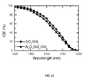
Figure 12 is a graph showing the relation between Internal Quantum Efficiency (IQE) and wavelength at high wavelengths, for passivated emitter and rear cell-type cells, compared for different rear surface passivation stacks. - In the different drawings, the same reference signs refer to the same or analogous elements.
- In the following detailed description, numerous specific details are set forth in order to provide a thorough understanding of the disclosure and how it may be practiced in particular embodiments. However, it will be understood that the present disclosure may be practiced without these specific details. In other instances, well-known methods, procedures and techniques have not been described in detail, so as not to obscure the present disclosure. While the present disclosure will be described with respect to particular embodiments and with reference to certain drawings, the disclosure is not limited hereto. The drawings included and described herein are schematic and are not limiting the scope of the disclosure. It is also noted that in the drawings, the size of some elements may be exaggerated and, therefore, not drawn to scale for illustrative purposes.
- Furthermore, the terms first, second, third and the like in the description, are used for distinguishing between similar elements and not necessarily for describing a sequence, either temporally, spatially, in ranking or in any other manner. It is to be understood that the terms so used are interchangeable under appropriate circumstances and that the embodiments of the disclosure described herein are capable of operation in other sequences than described or illustrated herein.
- Moreover, the terms top, bottom, over, under and the like in the description are used for descriptive purposes and not necessarily for describing relative positions. It is to be understood that the terms so used are interchangeable under appropriate circumstances and that the embodiments of the disclosure described herein are capable of operation in other orientations than described or illustrated herein.
- It is to be noticed that the term "comprising" should not be interpreted as being restricted to the means listed thereafter; it does not exclude other elements or steps. It is thus to be interpreted as specifying the presence of the stated features, integers, steps or components as referred to, but does not preclude the presence or addition of one or more other features, integers, steps or components, or groups thereof. Thus, the scope of the expression "a device comprising means A and B" should not be limited to devices consisting only of components A and B.
- In the context of the present description, the front surface or front side of a photovoltaic cell or of a substrate is the surface or side adapted for being oriented towards a light source and thus for receiving illumination. The back surface, rear surface, back side or rear side of a photovoltaic cell or of a substrate is the surface or side opposite to the front surface or side.
- One embodiment relates to a method for forming a good, blister-free, surface passivation layer on a surface of a silicon substrate, the method comprising: depositing an Al2O3 layer on the surface, the Al2O3 layer having a thickness not exceeding about 10 nm, e.g. in the range between about 1nm or 2 nm and 10 nm; performing an outgassing process at a temperature in the range between about 500ºC and 850ºC; and, after the outgassing process, depositing at least one additional dielectric layer such as a silicon nitride layer or a silicon oxide layer on the Al2O3 layer.
- It is an advantage of a method according to one embodiment that it leads to surface passivation layers with a good surface passivation quality that is maintained even after further processing performed at high temperatures. In one embodiment, before capping the Al2O3 layer with any additional layer, an outgassing process is performed. The Al2O3 layer is made sufficiently thin such that it doesn't form a barrier for the gases, i.e. such that gasses can diffuse through the thin Al2O3 layer, thus avoiding blister formation during outgassing. As gases are released before capping the Al2O3 layer with any other layer, also blister formation in a later stage of the process, e.g. under the influence of further high-temperature processes after capping of the Al2O3 layer, is avoided
- In one embodiment, the method may be used for the rear surface passivation of silicon photovoltaic cells, such as PERC-type or PERL-type cells, wherein a metal firing process is performed after forming the surface passivation layer. When using a method according to one embodiment, it is avoided that such metal firing process leads to a significant deterioration of the surface passivation quality. More in particular, the partial delamination of the Al2O3 passivation layer and the formation of blisters at an interface between the silicon substrate and the Al2O3 surface passivation layer is avoided.
- Experiments were performed wherein 30 nm thick Al2O3 layers were deposited by thermal ALD at 200°C on 0.4 Ohm-cm p-type FZ silicon wafers. After Al2O3 deposition a forming gas annealing process was performed for 30 minutes, at different annealing temperatures in the range between 200ºC and 900ºC.
Figure 1 shows the maximum effective minority carrier lifetimes as measured by quasi steady state photo conductance (QSSPC) as a function of the annealing temperature. In one embodiment, the highest effective lifetimes were obtained for annealing temperatures in the range between about 350ºC and 400ºC. For annealing temperatures above about 400°C, the effective lifetime decreases. It was observed that at these higher annealing temperatures blisters appear, and that for increasing annealing temperature the size of the blisters increases. For example, annealing at 400°C leads to blisters with a radius in the order of 1 micrometer; annealing at 430°C results in blisters with a radius in the order of 2 micrometer; after annealing at 470°C a blister radius in the order of 3 micrometer was measured, and after annealing at 500°C the blister radius was in the order of 3.5 micrometer. - Using an atmospheric pressure rapid thermal processing (RTP) chamber with atmospheric pressure ionization mass spectrometry (APIMS), desorbing species upon heating the Si / Al2O3 samples were identified.
Figure 2(a) shows desorption spectra for m/e (mass to charge ratio) = 18 (H2O+) and 29 (N2H+), an indication of desorption of H2O and H2, respectively.Figure 2(b) shows (i) spectra from m/e = 15 to 70, except those related to N2, H2O, O2 and CO2 (hence, m/e = 17-19, 28-29, 32, 35-37, 41-42, 44, 46, 50, 55-57, 60 are eliminated), where interferences are too large, and (ii) all spectra from m/e = 71 to 100. Spectra are displayed for a Si sample with 30 nm Al2O3 deposited at 200 °C and for a dummy wafer (background). From the measurements shown inFigure 2(a) andFigure 2(b) it can be concluded that desorption peaks can be observed immediately above 400°C for all spectra. - Based on these observations, it can be concluded that the formation of blisters at the Si / Al2O3 interface upon heating at temperatures above about 400ºC (
Figure 1 ) may be related to gaseous desorption at such temperatures (Figure 2 ). - ALD Al2O3 layers with a thickness of 30 nm were deposited on a silicon wafer at a deposition temperature of 200ºC. After Al2O3 deposition the wafer was heated to a temperature (continuously increasing temperature) ranging from 180ºC to 900ºC.
Figure 3 shows the measured desorption spectrum (open squares) for m/z (atomic mass unit) = 43, which may be an indication for H2O. It can be seen that outgassing mainly starts from a temperature of about 400ºC. It was observed that also blistering starts at an annealing temperature of about 400ºC or more.Figure 3 also shows the measured effective lifetime (full squares) for different samples that were annealed at different temperatures. A strong correlation with the outgassing profile was found, with the highest effective lifetime for annealing at a temperature of about 400ºC and a steeply decreasing lifetime for higher annealing temperatures, going to effective lifetimes close to zero for annealing temperatures higher than about 700ºC. These results indicate that a 30 nm thick Al2O3 layer forms a barrier for gas desorption, leading to blister formation when an annealing process is done at temperatures higher than about 400ºC. A similar trend was observed for other Al2O3 layers thicker than about 15 nm. -
Figure 4 shows the hydrogen concentration as a function of depth for a sample with an 100 nm thick as-deposited Al2O3 layer without blisters (diamonds), for a sample that was annealed at 500ºC after Al2O3 deposition (squares) and for a sample that was annealed at 600ºC after Al2O3 deposition (triangles). In the graph shown inFigure 4 , a depth = 0 corresponds to the Al2O3 surface and a depth = 1000 corresponds to the Si/Al2O3 interface. In an as-deposited layer the hydrogen content is substantially uniform within the Al2O3 layer. After annealing there is a clear non-uniformity of the hydrogen content, with substantially more hydrogen remaining at the Si/Al2O3 interface as compared to the Al2O3 surface. - ALD Al2O3 layers with a thickness of 5 nm were grown on a silicon wafer at a deposition temperature of 200ºC. After Al2O3 deposition the wafer was exposed to a continuously increasing temperature ranging from 180ºC to 900ºC.
Figure 5 shows the measured desorption spectrum (open squares) for m/z = 43. It can be seen that also here outgassing mainly occurs from a temperature of about 400ºC. However, for this sample no blistering was observed for the full range of annealing temperatures. From these results it can be concluded that an about 5 nm thick Al2O3 layer is sufficiently thin to allow outgassing, without blister formation. This is opposed to the results shown inFigure 3 for a 30 nm thick Al2O3 layer, where outgassing leads to blister formation.Figure 5 also shows the measured effective lifetime (full squares) for samples annealed at different temperatures. The highest lifetime was measured for an annealing temperature of about 500ºC. At higher annealing temperatures the effective lifetime decreases, but the decrease in lifetime is much less than for the sample having a 30 nm thick Al2O3 layer (Figure 3 ). - An example of a prior art PERC-type silicon cell processing method is depicted in
Fig. 7 . It comprises: single side texturing of a substrate (e.g. silicon wafer); performing a cleaning step; emitter diffusion at a temperature in the range between 800ºC and 950ºC in a POCl3 diffusion furnace, resulting in doped region both at the front side and at the rear side of the substrate; removal of the doped (emittter) region at the rear side; removal of the PSG (PhosphoSilicate Glass) formed during emitter diffusion at the front surface; performing a cleaning step; providing a passivation stack at the rear side; depositing an ARC (antireflection coating), e.g. a SiNx ARC at the front side; local opening of the passivation stack at the rear side, for example by laser ablation; performing a rear side metallization step and a front side metallization step; and cofiring of the rear side metallization and the front side metallization at a temperature in the range between 600ºC and 1000ºC. - In a method for fabricating PERC-type silicon cells with a rear side Al2O3 passivation layer, at the rear side of the cells the Al2O3 layer is capped with an additional dielectric layer such as a SiNx layer and/or a SiOx layer, the additional dielectric layer acting as a barrier for the Al metal layer during a contact firing process and providing a good rear internal reflection of long wavelength light (e.g. wavelength larger than 900 nm). Such capping layer is typically deposited at a temperature at or above about 400ºC, or above 400°C, or above 500°C. Thus, this capping layer deposition can act as an annealing process, leading to blister formation as illustrated above. In addition, providing the capping layer enlarges the layer thickness and thus the gas barrier thickness, leading to an even higher risk of blister formation. Also, in PERC-type cells, at the end of the fabrication process a metal cofiring process is typically performed at a temperature higher than about 835ºC, again leading to blister formation problems. One embodiment provides a solution to the blister formation problem by using a thin Al2O3 layer (≤ about 10 nm) and by performing an outgassing process at a temperature in the range between about 500ºC and 850ºC before capping of the Al2O3 layer.
- PERC-type (passivated emitter and rear contacts) photovoltaic cells were fabricated, wherein a method according to one embodiment was used for rear surface passivation. As a substrate, 125 mm x 125 mm semi-square p-type Cz silicon wafers with a resistivity of 0.5 to 3 Ohm-cm were used. After texturing of the substrate, the rear side of the substrate was polished, resulting in a substrate thickness of 160 micrometer. Next a front-side phosphorous diffusion process (POCl3 diffusion) was performed for forming an emitter region having a sheet resistance of 60 Ohm per square. The wafers were then cleaned in a 1:4 H2O2:H2SO4 solution at 85ºC for 10 minutes, followed by an HF-dip (2% HF in deionized water) and hot air drying. Next a PECVD SiNx antireflection coating was deposited at the front side. Then the wafers were cleaned and dried using an advanced drying method. For a first part of the wafers, a cleaning method leading to a hydrophobic surface (Si-H) was used. More in particular, these wafers were cleaned in a 1:4 H2O2:H2SO4 solution at 85ºC for 10 minutes, followed by an HF-dip (2% HF in deionized water) and Marangoni drying. For a second part of the wafers, a cleaning method leading to a hydrophilic surface (Si-OH) was used. More in particular, these wafers were cleaned in a 1:4 H2O2:H2SO4 solution at 85ºC for 10 minutes, followed by an HF-dip (2% HF in deionized water), chemical oxidation in NH4OH:H2O2:H2O (1:1:5) for 10 minutes at ambient temperature and finally Marangoni drying. A thin Al2O3 layer (
thickness 5 nm or 10 nm) was then deposited on the rear surface using thermal ALD at 200ºC, and an annealing process (outgassing process) in a nitrogen environment was done at three different temperatures (400ºC, 500ºC and 600ºC). A PECVD SiNx capping layer was deposited on the Al2O3 layer. At the rear side of the cell contact openings were made through the Al2O3/SiNx stack using laser ablation. This was followed by Al sputtering at the rear side for forming rear side contacts and Ag screen printing at the front side for forming front side contacts, and cofiring of the metal contacts at 860ºC peak temperature. - Measured open-circuit voltages for different cells are shown in
Figure 6 . As a reference, also the open-circuit voltage of a cell with a full Al BSF (back surface field) is shown, as well as the open-circuit voltage of a PERC cell having a stack comprising a silicon oxide layer and a silicon nitride layer as a rear surface passivation stack. From these results, it can be concluded that the open-circuit voltage increases for increasing outgassing temperature, thus indicating a better surface passivation quality for increasing outgassing temperature. Outgassing at about 400ºC does not lead to a significant improvement as compared to the reference PERC cell. For the same outgassing conditions, higher open-circuit voltages are obtained for cells having an about 5 nm thick Al2O3 layer as compared to cells having an about 10 nm thick Al2O3 layer. -
Figure 8 compares the reflectance between 1000 nm and 1200 nm of PERC-type solar cells on 150 micrometer thick p-type Cz Si substrates with alkaline-textured front surface and polished rear surface passivated by a stack of Al2O3/SiNx, SiOx/SiNx or Al2O3/SiOx/SiNx. For the SiOx layer, two thicknesses have been used, where SiOx(A) is thinner compared with SiOx(B). From these reflectance measurements, it is clear that for optimal rear internal reflection of an Al2O3-based rear surface passivation, it is preferably capped with a thick-enough SiOx layer and SiNx. These rear surface passivation stacks have been optimized in the prior art. This means that for optimal rear internal reflection, the Al2O3 has to be capped with SiOx/SiNx before the co-firing step (see also Table I). Capping a thin ALD Al2O3 film with SiOx and/or SiNx or annealing a stack of Al2O3 and SiOx and/or SiNx can lead to blister formation. Blistering is the partial delamination of an Al2O3-based stack caused by gaseous desorption in the Al2O3 layer upon thermal treatments above a critical temperature (typically 350°C for ALD Al2O3); the capped Al2O3 layer acts as a gas barrier and blister formation occurs. Blistering of Al2O3 and capped Al2O3 layers has been observed for various deposition techniques: for thermal ALD, plasma enhanced ALD and PECVD. Using a thin enough (≤10nm) Al2O3 layer and performing an annealing step prior to capping in accordance with the present disclosure are shown to be the solution to create blister-free Al2O3-based passivation stacks. - An enhanced internal reflection of the Al2O3-based rear surface passivation stack is thereby achieved.
- In order to study the thermal stability of the Al2O3-based rear surface passivation stack, blister-free screen-printed large-area p-type Si PERC-type solar cells were made as indicated in Table I, using an "outgassing" thermal treatment for 20min in N2 after the Al2O3 deposition (
thickness 10 nm) and prior to the SiOx/SiNx capping.Table I. Baseline p-type Cz Si passivated emitter and rear cell (PERC)-type solar cells, having an (Al2O3 )/SiOx /SiNx rear surface passivation stack. The 148.25-cm2 cells are 150-mm thick, have a base resistivity of 1Ωcm and an emitter of 60Ω/sq. - Texturing/polishing - POCl3 diffusion (60Ω/sq) - Rear side emitter removal - SiNx ARC front - Passivation rear (Al2O3)/SiOx/SiNx - Laser ablation rear - Physical vapor deposition Al rear/screen-printing Ag front - Co-firing -
Figure 9 shows the open-circuit voltage VOC (filled circles) of these cells as a function of the out-gassing temperature. Also the blistering surface coverage Y (filled squares) for the Al2O3/SiOx/SiNx stack is shown, as measured by optical microscopy. As a reference, the VOC of SiOx/SiNx-passivated PERC is also given.Figure 10 gives the calculated effective rear surface recombination velocity (Seff,rear), with Z being the fraction of blistering contacted during co-firing. The VOC depicted inFigure 11 is simulated from the Seff,rear values shown inFigure 10 . The filled circles inFigure 11 show measured Voc values. The Seff,rear and VOC inFigure 10 and11 are calculated as a function of out-gassing temperature as well. - As can be seen in
Figure 9 , the average VOC of the Al2O3/SiOx/SiNx-passivated PERC-type cells clearly improves as a function of out-gassing temperature. Even more, after out-gassing at 600-700°C, the Al2O3/SiOx/SiNx passivated cells are clearly better passivated at the rear compared with the SiOx/SiNx passivated cells. Together with this improvement in VOC, there is an obvious decrease in blistering as a function of outgassing temperature. By using this fraction of blistering and a factor Z for the probability of contacting through a blister during co-firing, an estimation of Seff,rear is obtained (Figure 10 ). Simulating the expected VOC using this Seff,rear, it is very clear that the increase in measured VOC as a function of out-gassing temperature is directly linked to the decrease in blistering. If the out-gassing temperature is too low during co-firing, about 30% of the blisters (corresponding to Z = 0.3) become local point contacts; hence, the Seff,rear increases and consequently the VOC decreases. For out-gassing temperatures above 800°C, the Seff,rear starts to increase again. - Integration of Al2O3/SiOx/SiNx as rear surface passivation for p-type Si PERC solar cells, in combination with an out-gassing step, has been shown to be advantageous. The average and best cell results for the Al2O3/SiOx/SiNx passivated PERC-type solar cells out-gassed at 700°C after the Al2O3 and prior to the SiOx/SiNx deposition steps are listed in Table II.
Table II. Overview of the cell characterization results (AM 1.5G) for the 148 25-cm2 (Al2O3)/SiOx/SiNx passivated p-type Cz Si PERC-type solar cells. The processing sequence is given in Table I. The cells are 150-µm thick and have a base resistivity of 1 Ωcm. Rear surface passivation Size (cm2) J SC (mA/cm2) V OC (mV) FF (%) Eta (%) Al2O3/SiO x /SiN x Average (four cells) 148.25 38.0±0.2 643±1 77.6±0.2 19.0±0.1 Best cell 148.25 38.2 645 77.7 19.1 SiO x /SiN x Best cell 148.25 37.8 638 77.7 18.7 - Also the best reference SiOx/SiNx-passivated PERC-type solar cell result is given. The internal quantum efficiency (IQE) at high wavelength is shown for both SiOx/SiNx and Al2O3/SiOx/SiNx passivated cells in
Figure 12 . As seen in Table II, for Al2O3/SiOx/SiNx-passivated PERC-type solar cells, an optimum reaching an average cell efficiency of 19.0% is found, as compared with 18.7% for the best SiOx/SiNx-passivated solar cell. - There is an obvious gain in VOC and JSC of 7mV and 0.4 mA/cm2, respectively, thanks to enhanced rear surface passivation and rear internal reflection. This improved Al2O3/SiOx/SiNx rear surface passivation is also confirmed by the IQE measurements at wavelengths between 1000 and 1200 nm as shown in
Figure 12 . - The foregoing description details certain embodiments of the disclosure. It will be appreciated, however, that no matter how detailed the foregoing appears in text, the disclosure may be practiced in many ways. It should be noted that the use of particular terminology when describing certain features or aspects of the disclosure should not be taken to imply that the terminology is being re-defined herein to be restricted to including any specific characteristics of the features or aspects of the disclosure with which that terminology is associated.
- While the above detailed description has shown, described, and pointed out novel features of the disclosure as applied to various embodiments, it will be understood that various omissions, substitutions, and changes in the form and details of the device or process illustrated may be made by those skilled in the technology.
Claims (11)
- A method for forming a surface passivation layer on a surface of a crystalline silicon substrate, the method comprising:- depositing an Al2O3 layer on said surface, the Al2O3 layer having a thickness not exceeding 15nm;- performing an outgassing process at a temperature in the range between 500ºC and 900ºC, after said deposition of said Al2O3 layer on said surface;- after the outgassing process, depositing at least one additional dielectric layer such as a silicon nitride layer and/or a silicon oxide layer on the Al2O3 layer.
- A method according to claim 1, wherein depositing said Al2O3 layer on said surface, comprises depositing a Al2O3 layer having a thickness not exceeding 10nm.
- A method according to claim 1 or 2, wherein said out-gassing process is performed at a temperature between 700°C and 850°C.
- Method according to any of the previous claims, wherein the outgassing process is performed in a nitrogen environment.
- Method according to any of the previous claims, wherein the duration of the out-gassing process is between 5 and 30 minutes.
- Method according to any of the previous claims, further comprising processing said crystalline silicon substrate further toward a silicon solar cell, at least partially comprising processing at temperatures in the range between about 400ºC and 900ºC.
- Method according to any of the previous claims, wherein said Al2O3 layer is deposited by ALD (atomic layer deposition) at a temperature in the range between 150ºC and 250ºC.
- Method according to any of the previous claims 1 to 6, wherein said Al2O3 layer is deposited by PECVD (plasma enhanced chemical vapour deposition) at a temperature in the range between 150ºC and 350ºC.
- Method according to any of the previous claims, used for the rear surface passivation of silicon photovoltaic cells, wherein a metal firing process is performed after forming the Al2O3 surface passivation layer and after capping the surface passivation layer with at least one additional dielectric layer, the additional dielectric layer forming a barrier against metal spiking during firing and improving back reflectance for the silicon photovoltaic cell.
- Method according to claim 9, wherein said metal firing process is performed at a temperature higher than 835ºC,
- Method according to any of the previous claims, further comprising cleaning said surface before depositing said Al2O3 layer on said surface, by means of a cleaning method leading to a hydrophilic surface.
Applications Claiming Priority (1)
| Application Number | Priority Date | Filing Date | Title |
|---|---|---|---|
| US201161493920P | 2011-06-06 | 2011-06-06 |
Publications (2)
| Publication Number | Publication Date |
|---|---|
| EP2533305A2 true EP2533305A2 (en) | 2012-12-12 |
| EP2533305A3 EP2533305A3 (en) | 2014-05-21 |
Family
ID=46513629
Family Applications (1)
| Application Number | Title | Priority Date | Filing Date |
|---|---|---|---|
| EP12170534.7A Withdrawn EP2533305A3 (en) | 2011-06-06 | 2012-06-01 | Method for blister-free passivation of a silicon surface |
Country Status (4)
| Country | Link |
|---|---|
| US (1) | US8557718B2 (en) |
| EP (1) | EP2533305A3 (en) |
| JP (1) | JP2012253356A (en) |
| TW (1) | TW201320188A (en) |
Cited By (2)
| Publication number | Priority date | Publication date | Assignee | Title |
|---|---|---|---|---|
| DE102013110421A1 (en) | 2013-09-20 | 2015-04-16 | Helmholtz-Zentrum Berlin Für Materialien Und Energie Gmbh | Process for the preparation of structured a-SiNx layers and their use |
| WO2016022026A1 (en) | 2014-08-04 | 2016-02-11 | Asm International N.V. | A photovoltaic cell with a passivation layer as well as a method for manufacturing such a photovoltaic cell |
Families Citing this family (14)
| Publication number | Priority date | Publication date | Assignee | Title |
|---|---|---|---|---|
| KR101889775B1 (en) | 2012-09-27 | 2018-08-20 | 엘지전자 주식회사 | Solar cell and method for manufacturing the smae |
| CN104037242B (en) * | 2013-03-06 | 2016-03-16 | 中美硅晶制品股份有限公司 | Photovoltaic element and method for manufacturing same |
| US9575018B2 (en) * | 2013-09-16 | 2017-02-21 | Cerium Laboratories, Llc | System and method for testing ceramic coatings |
| KR101507767B1 (en) | 2013-11-07 | 2015-04-07 | 충남대학교산학협력단 | Manufacturing Method of Solar Cell |
| CN106463548B (en) * | 2014-05-29 | 2018-07-24 | 京瓷株式会社 | Solar cell device and solar cell module |
| EP3306674B1 (en) | 2015-05-27 | 2021-06-23 | Kyocera Corporation | Solar cell element and method for manufacturing same |
| JP2017120873A (en) | 2015-12-25 | 2017-07-06 | 京セラ株式会社 | Insulating paste, method for producing the same, and method for producing solar cell element |
| JP6203990B1 (en) | 2016-02-26 | 2017-09-27 | 京セラ株式会社 | Solar cell element |
| EP3493272B1 (en) | 2016-07-28 | 2022-04-27 | Kyocera Corporation | Solar cell element and method for manufacturing solar cell element |
| CN109216473B (en) | 2018-07-20 | 2019-10-11 | 常州大学 | Surface interface passivation layer and passivation method of a kind of crystalline silicon solar cell |
| CN109585597A (en) * | 2018-10-12 | 2019-04-05 | 浙江爱旭太阳能科技有限公司 | A method of improving tubular type crystal silicon solar PERC battery front side around plating |
| KR102967998B1 (en) | 2020-10-06 | 2026-05-22 | 삼성전자주식회사 | Image sensor |
| CN118215985A (en) | 2021-09-20 | 2024-06-18 | 应用材料公司 | Germanium and Silicon Stacking for 3D NAND |
| CN120500161A (en) * | 2025-05-21 | 2025-08-15 | 滁州捷泰新能源科技有限公司 | Solar cell composite passivation layer, preparation method thereof and solar cell |
Family Cites Families (3)
| Publication number | Priority date | Publication date | Assignee | Title |
|---|---|---|---|---|
| DE102007054384A1 (en) * | 2007-11-14 | 2009-05-20 | Institut Für Solarenergieforschung Gmbh | Method for producing a solar cell with a surface-passivating dielectric double layer and corresponding solar cell |
| KR20090100951A (en) * | 2008-03-21 | 2009-09-24 | 삼성전자주식회사 | Nonvolatile Memory Device and Formation Method |
| EP2482328A2 (en) * | 2011-01-31 | 2012-08-01 | Imec | Fabrication method for local back contact photovoltaic cells |
-
2012
- 2012-06-01 EP EP12170534.7A patent/EP2533305A3/en not_active Withdrawn
- 2012-06-05 TW TW101120049A patent/TW201320188A/en unknown
- 2012-06-05 JP JP2012127996A patent/JP2012253356A/en active Pending
- 2012-06-05 US US13/489,305 patent/US8557718B2/en not_active Expired - Fee Related
Non-Patent Citations (1)
| Title |
|---|
| None |
Cited By (4)
| Publication number | Priority date | Publication date | Assignee | Title |
|---|---|---|---|---|
| DE102013110421A1 (en) | 2013-09-20 | 2015-04-16 | Helmholtz-Zentrum Berlin Für Materialien Und Energie Gmbh | Process for the preparation of structured a-SiNx layers and their use |
| DE102013110421B4 (en) | 2013-09-20 | 2020-07-30 | Helmholtz-Zentrum Berlin für Materialien und Energie Gesellschaft mit beschränkter Haftung | Use of a structured a-SiNx layer |
| WO2016022026A1 (en) | 2014-08-04 | 2016-02-11 | Asm International N.V. | A photovoltaic cell with a passivation layer as well as a method for manufacturing such a photovoltaic cell |
| NL2013298B1 (en) * | 2014-08-04 | 2016-09-21 | Asm Int Nv | A Photovoltaic cell with a passivation layer as well as a method for manufacturing such a photovoltaic cell. |
Also Published As
| Publication number | Publication date |
|---|---|
| EP2533305A3 (en) | 2014-05-21 |
| JP2012253356A (en) | 2012-12-20 |
| TW201320188A (en) | 2013-05-16 |
| US20120306058A1 (en) | 2012-12-06 |
| US8557718B2 (en) | 2013-10-15 |
Similar Documents
| Publication | Publication Date | Title |
|---|---|---|
| US8557718B2 (en) | Method for blister-free passivation of a silicon surface | |
| US20230074411A1 (en) | Solar cell, method for manufacturing solar cell, and solar cell module | |
| CN106463548B (en) | Solar cell device and solar cell module | |
| US9660130B2 (en) | Passivation stack on a crystalline silicon solar cell | |
| EP2482328A2 (en) | Fabrication method for local back contact photovoltaic cells | |
| JP2013524549A (en) | Multilayer SiN for functional and optical graded ARC layers on crystalline solar cells | |
| TW201203592A (en) | Oxide nitride stack for backside reflector of solar cell | |
| CN115332390B (en) | Solar cell and method for manufacturing the same | |
| Vermang et al. | On the blistering of atomic layer deposited Al 2 O 3 as Si surface passivation | |
| Vermang et al. | Spatially-separated atomic layer deposition of Al 2 O 3, a new option for high-throughput si solar cell passivation | |
| Yadav et al. | Comparative study of different silicon oxides used as interfacial passivation layer (SiNy: H/SiOx/n+-Si) in industrial monocrystalline silicon solar cells | |
| CN102386277B (en) | Multi-coating technology | |
| US20110136285A1 (en) | Method for manufacturing stacked film and solar cell | |
| US8735201B2 (en) | Film-forming method for forming passivation film and manufacturing method for solar cell element | |
| WO2014045193A1 (en) | Method for reducing contact resistances of screen printed contacts | |
| CN120076477A (en) | Passivation contact structure and preparation method and application thereof | |
| CN113659032B (en) | PERC battery avoiding aluminum oxide passivation and method for making passivation layer of battery | |
| Rohatgi et al. | Rapid thermal processing of next generation silicon solar cells | |
| Bruhat et al. | Contacting n+ poly-Si junctions with fired AZO layers: a promising approach for high temperature passivated contact solar cells | |
| Jeon et al. | Effect of HF treatment on hydrogenated silicon nitride anti-reflection films quality and optical properties | |
| CN119486365A (en) | Solar cell and preparation method thereof, photovoltaic module | |
| CN121358049A (en) | Passivation methods, fabrication methods, photovoltaic modules and photovoltaic systems for solar cells | |
| CN120676758A (en) | TOPCon battery structure and preparation method thereof | |
| Shin et al. | Characteristics of Al2O3 Films Deposited by Plasma-Assisted Atomic Layer Deposition with Varying RF Powers | |
| CN120981039A (en) | A positive film structure and preparation method for improving UV degradation in TOPCon batteries |
Legal Events
| Date | Code | Title | Description |
|---|---|---|---|
| PUAI | Public reference made under article 153(3) epc to a published international application that has entered the european phase |
Free format text: ORIGINAL CODE: 0009012 |
|
| AK | Designated contracting states |
Kind code of ref document: A2 Designated state(s): AL AT BE BG CH CY CZ DE DK EE ES FI FR GB GR HR HU IE IS IT LI LT LU LV MC MK MT NL NO PL PT RO RS SE SI SK SM TR |
|
| AX | Request for extension of the european patent |
Extension state: BA ME |
|
| PUAL | Search report despatched |
Free format text: ORIGINAL CODE: 0009013 |
|
| AK | Designated contracting states |
Kind code of ref document: A3 Designated state(s): AL AT BE BG CH CY CZ DE DK EE ES FI FR GB GR HR HU IE IS IT LI LT LU LV MC MK MT NL NO PL PT RO RS SE SI SK SM TR |
|
| AX | Request for extension of the european patent |
Extension state: BA ME |
|
| RIC1 | Information provided on ipc code assigned before grant |
Ipc: H01L 31/18 20060101AFI20140416BHEP |
|
| STAA | Information on the status of an ep patent application or granted ep patent |
Free format text: STATUS: THE APPLICATION IS DEEMED TO BE WITHDRAWN |
|
| 18D | Application deemed to be withdrawn |
Effective date: 20141122 |