EP2530831A1 - Audio amplifier circuit and method of operation thereof - Google Patents
Audio amplifier circuit and method of operation thereof Download PDFInfo
- Publication number
- EP2530831A1 EP2530831A1 EP12169862A EP12169862A EP2530831A1 EP 2530831 A1 EP2530831 A1 EP 2530831A1 EP 12169862 A EP12169862 A EP 12169862A EP 12169862 A EP12169862 A EP 12169862A EP 2530831 A1 EP2530831 A1 EP 2530831A1
- Authority
- EP
- European Patent Office
- Prior art keywords
- signal
- input
- designed
- output
- audio
- Prior art date
- Legal status (The legal status is an assumption and is not a legal conclusion. Google has not performed a legal analysis and makes no representation as to the accuracy of the status listed.)
- Granted
Links
Images


Classifications
-
- H—ELECTRICITY
- H03—ELECTRONIC CIRCUITRY
- H03F—AMPLIFIERS
- H03F3/00—Amplifiers with only discharge tubes or only semiconductor devices as amplifying elements
- H03F3/181—Low-frequency amplifiers, e.g. audio preamplifiers
-
- H—ELECTRICITY
- H03—ELECTRONIC CIRCUITRY
- H03F—AMPLIFIERS
- H03F1/00—Details of amplifiers with only discharge tubes, only semiconductor devices or only unspecified devices as amplifying elements
- H03F1/02—Modifications of amplifiers to raise the efficiency, e.g. gliding Class A stages, use of an auxiliary oscillation
- H03F1/0205—Modifications of amplifiers to raise the efficiency, e.g. gliding Class A stages, use of an auxiliary oscillation in transistor amplifiers
- H03F1/0211—Modifications of amplifiers to raise the efficiency, e.g. gliding Class A stages, use of an auxiliary oscillation in transistor amplifiers with control of the supply voltage or current
-
- H—ELECTRICITY
- H03—ELECTRONIC CIRCUITRY
- H03F—AMPLIFIERS
- H03F3/00—Amplifiers with only discharge tubes or only semiconductor devices as amplifying elements
- H03F3/72—Gated amplifiers, i.e. amplifiers which are rendered operative or inoperative by means of a control signal
-
- H—ELECTRICITY
- H03—ELECTRONIC CIRCUITRY
- H03G—CONTROL OF AMPLIFICATION
- H03G3/00—Gain control in amplifiers or frequency changers
- H03G3/20—Automatic control
- H03G3/30—Automatic control in amplifiers having semiconductor devices
- H03G3/32—Automatic control in amplifiers having semiconductor devices the control being dependent upon ambient noise level or sound level
-
- H—ELECTRICITY
- H03—ELECTRONIC CIRCUITRY
- H03G—CONTROL OF AMPLIFICATION
- H03G3/00—Gain control in amplifiers or frequency changers
- H03G3/20—Automatic control
- H03G3/30—Automatic control in amplifiers having semiconductor devices
- H03G3/34—Muting amplifier when no signal is present
- H03G3/341—Muting when no signals or only weak signals are present
-
- H—ELECTRICITY
- H03—ELECTRONIC CIRCUITRY
- H03G—CONTROL OF AMPLIFICATION
- H03G3/00—Gain control in amplifiers or frequency changers
- H03G3/20—Automatic control
- H03G3/30—Automatic control in amplifiers having semiconductor devices
- H03G3/34—Muting amplifier when no signal is present
- H03G3/344—Muting responsive to the amount of noise (noise squelch)
-
- H—ELECTRICITY
- H03—ELECTRONIC CIRCUITRY
- H03F—AMPLIFIERS
- H03F2200/00—Indexing scheme relating to amplifiers
- H03F2200/03—Indexing scheme relating to amplifiers the amplifier being designed for audio applications
-
- H—ELECTRICITY
- H03—ELECTRONIC CIRCUITRY
- H03F—AMPLIFIERS
- H03F2200/00—Indexing scheme relating to amplifiers
- H03F2200/393—A measuring circuit being coupled to the output of an amplifier
-
- H—ELECTRICITY
- H03—ELECTRONIC CIRCUITRY
- H03F—AMPLIFIERS
- H03F2200/00—Indexing scheme relating to amplifiers
- H03F2200/78—A comparator being used in a controlling circuit of an amplifier
-
- H—ELECTRICITY
- H03—ELECTRONIC CIRCUITRY
- H03F—AMPLIFIERS
- H03F2203/00—Indexing scheme relating to amplifiers with only discharge tubes or only semiconductor devices as amplifying elements covered by H03F3/00
- H03F2203/72—Indexing scheme relating to gated amplifiers, i.e. amplifiers which are rendered operative or inoperative by means of a control signal
- H03F2203/7212—Indexing scheme relating to gated amplifiers, i.e. amplifiers which are rendered operative or inoperative by means of a control signal the gated amplifier being switched on or off by switching off or on a feedback control loop of the amplifier
Definitions
- the present disclosure relates to an audio amplifier circuit and method of operation thereof.
- circuit and method find their use in audio amplifiers designed for use in the automotive industry.
- an amplifier supplied with a typical automotive battery voltage supply i.e., 14.4V, dissipates energy even when it does not deliver power.
- the dissipated power may be estimated to be about 0.5 - 1 W per channel, even when power is not delivered through a channel of the amplifier.
- One embodiment of this disclosure is obviates the problems discussed above with reference to the prior art.
- One embodiment of the present disclosure is an audio amplifier circuit having the features of claim 1.
- One embodiment of the present disclosure is a method of optimizing the efficiency of an audio amplifier circuit having the features of claim 14.
- Some embodiments of the present disclosure provide a circuit and a method that can be used to reduce power losses caused by power dissipated even when no power is delivered through a channel of the audio amplifier.
- numeral 1 designates an audio amplifier, which is designed to provide an output signal Vout to an audio transducer 2, such as a loudspeaker as is usually installed in a car.
- the audio amplifier circuit 1 comprises:
- the noise component Vn of the Sdet signal is the background or ambient noise as detected by the sensor 4.
- the senor 4 is adapted to detect at least the background noise or ambient noise Vn when no audible sound Vs is emitted through the acoustic transducer 2.
- the amplifier 3 has been advantageously designed to be off if the output signal Vout is zero or lower than a threshold value Vth.
- the threshold value Vth is the minimum limit below which the user cannot hear sounds, whether these are background noise Vn or audible signals Vs.
- the threshold value Vth is equal to a value that corresponds to a sound intensity of 10 -12 W/m 2 .
- audibility threshold value Vth may be expressed not only in terms of sound intensity, but also in equivalent terms of sound pressure, i.e. , 0.000002 Pa or in terms of decibel, i.e., 0 dB.
- the ambient noise component Vn is higher, and the minimum audibility threshold for the reproduced audio signal is also increased.
- the circuit 1 comprises a processing block 5, which is designed to receive the detected signal Sdet at its input and to generate a switch-off signal Soff at its output, the latter signal being input to the audio power amplifier 3.
- the processing block 5 processes the detected signal Sdet according to the input signal Sin to identify the noise component Vn in the detected signal Sdet, to generate a reference signal Smod'.
- the block 5 If the input signal Sin is lower than the reference signal value Smod', then the block 5 generates the switch-off signal Soff, to switch off the output channel of the amplifier 3 whose level is lower than the audible threshold value.
- the signal Smod' represents the reference or threshold value below which no sound is audible by the listener.
- the processing block 5 also generates a signal Sgain' at its output, the latter signal being input to the power amplifier 3, to set the gain of the power amplifier 3 to a minimum value.
- the processing block 5 may include an adaptive filter block 7, which is designed to filter said input signal Sin according to said detected signal Sdet, to generate a filtered signal Sfil.
- the adaptive filter block 7 is adapted to minimize the mean-square error of the signal Sdet according to the signal Sin.
- the adaptive filter 7 assumes that there is a strong correlation between the input signal Sin and the audible sound component Vs of the signal Sdet.
- the resulting signal is as close as possible to the signal component Vs of the signal Sdet, and hence subtraction of this signal from the signal Sdet provides the noise component Vn of the detected signal Sdet.
- the adaptive filter 7 outputs the filtered signal Sfil, which represents the background or ambient noise component Vn only of such detected signal Sdet.
- the adaptive filter 7 consists of a Least Mean Square (LMS) filter.
- LMS Least Mean Square
- the audio amplifier circuit 1 may comprise a delay block 8 which is designed to delay the input Sin by a predetermined interval of time to generate a delayed input signal at its output Sin,rit, which is advantageously input to the filter block 7.
- interval of time may be selected according to design specifications and is preset beforehand.
- the adaptive filter operates with the delayed input signal Sin,rit and the detected signal Sdet at its input, to generate the filtered signal Sfil.
- This processing block 5 may include an amplitude determining block 9, which is designed to receive the filtered signal Sfil at its input and generate a modulus signal Smod at its output representing the modulus of such filtered signal Sfil.
- the signal Smod is representative of the amplitude value of said filtered signal Sfil, i.e., the amplitude value of the background or ambient noise component Vn of such detected signal Sdet.
- the processing block 5 may include an on/off block 10, which is designed to receive the signal Smod at its input and is designed to generate the on/off signal Son/Soff and a signal gain Sgain at its output.
- the on/off block 10 generates the off signal Soff at its output if, at least during a first period of time T1 ranging from 70 msec to 130 msec, preferably 100 msec, the value of the input signal Sin is lower than the value of the reference signal Smod'.
- the minimum gain value for the amplifier 3 is reached within a time period T2 ranging from 10 msec to 30 msec, preferably 20 msec.
- the signal Sgain' allows the gain of the amplifier 3 to be set to its minimum value and to such minimum value to be reached within the period T2.
- the signal Sgain' is obtained by a gain block 6.
- Such gain bock 6 receives a Sgain signal generated by the on/off block 10 and the delayed input signal Sin,rit at its input, and generates the gain signal Sgain' that represents the actual gain value to be set in the amplifier, at its output.
- the audio amplifier circuit 1 may include a weighting filter block 11 which is designed according to the sensitivity of a human ear.
- the input signal Sin is input to the weighting filter block 11 to generate a signal Sin,pes, which is in turn input to the on/off block 10.
- the on/off block 10 (or more generally the block 5) generates the off signal Soff if the input signal Sin,pes is lower than the value of the reference signal Smod'.
- the processing block 5 confirms that the input signal Sin,pes is lower than or equal to the reference signal Smod' during the time T1 and that the volume of the amplifier 3 is lowered to the minimum within the time T2 using the signal Sgain', the amplifier 3 may be switched off.
- the amplifier 3 is immediately switched on using the signal Son, and the volume control is brought back to a zero attenuation value, or anyway to a working value, within an interval of time ranging from 7 msec to 13 msec, preferably of 10 msec.
- the circuit 1 is obviously more easily controlled in a digital environment, and the switching amplifier 3 may improve its behavior, because quick switching on/off is facilitated.
- the input signal Sin is preferably a digital signal
- the detected signal Sdet is converted into a digital form through an analog-to-digital conversion block (ADC) 20.
- ADC analog-to-digital conversion block
- the signal Sgain' is converted to analog by a digital-to-analog converter (DAC) 21 before being input to the amplifier 3.
- DAC digital-to-analog converter
- Figure 3 shows a possible embodiment of the on/off block 10
- Figure 4 shows its operation with time.
- the on/off block 10 has at its inputs the signal Smod and the input signal Sin or the version thereof that has been filtered by the weighting filter block 11 designed according to the sensitivity of a human ear, i.e., the signal Sin,pes.
- the latter is obtained by subtracting a predetermined constant quantity Q from the modulus signal Smod, i.e., the modulus noise component Vn of the signal Sdet.
- a summation node 12 is provided, which is designed to subtract the quantity Q, which is 20 dB in the diagram herein, from the modulus signal Smod, to generate the reference signal Smod'.
- the quantity Q represents the audibility threshold, below which the musical signal Vs cannot be heard.
- the signal Sin,pes is processed by an effective value converter 13, to obtain a Root Mean Square (RMS) signal Sin, pes'.
- RMS Root Mean Square
- a comparator block 14 is designed to compare the two signals Sin,pes' and Smod' and to generate a Selab signal at its output. Particularly, if the signal Sin,pes' is higher than the signal Smod', then the output of the comparator block 14, i.e., the signal Selab, is set to a high value.
- the on/off block 10 also includes a timer 15, a timer threshold block 15', a NAND gate 15", an integration block 16, a threshold block 17, and a NOT gate 18.
- the output of the comparator block 14 is coupled to respective inputs of the timer 15 and the NOT gate 18.
- the output of the timer 15 is coupled to the input of the timer threshold block 15' which has an output coupled to a first input of the NAND gate 15".
- the output of the NOT gate 18 is coupled to a second input of the NAND gate 15" which has an output coupled to an input of the integration block 16.
- any transition from a low value to a high value of the signal Selab causes the NOT gate to transition to a low value, which causes the NAND gate to output a high value.
- the transition from low to high of the signal Selab causes the timer 15 to be reset, which also causes the output of the timer threshold block 15' to be low.
- the timer threshold block 15 From the start of the timer 15, as soon as the preset threshold value of the period T1 (e.g. , 100 msec) is exceeded, the timer threshold block 15'outputs a high value to the first input of the NAND gate 15", which causes the output signal y of the NAND gate to go to zero. This causes the attenuation step to be started by the signal Sgain', which is operative on the volume control of the amplifier 3 and brings it to the minimum within the period T2, i.e. , within about 20 msec.
- the signal Sgain is obtained through the integration block 16, which is designed to perform an integration of the signal y.
- the amplifier 3 may be switched off by generation of the signal Soff.
- the sensor 4 also referring to Figure 2 , it is shown to comprise a microphone as generally used in the car-audio industry.
- This microphone detects the audible signal component Vs and the noise component Vn to generate the detected signal Sdet at its output.
- the signal Sdet is sent to the processing block 5 through a dedicated connection.
- a loudspeaker subjected to an acoustic pressure may be arranged to generate an electric signal.
- a dynamic loudspeaker is subjected to sound pressure, e.g. , only the sound pressure generated by the background noise component Vn in the interior of the car or the sound pressure generated by the audible component Vs and the noise component Vn, then it generates a signal that is proportional to the sound pressure itself.
- the signal generated by such dynamic loudspeaker is equal to the detected signal Sdet from the microphone.
- the existing connection of the loudspeaker 2 to the power amplifier 3 can transfer such signal Sdet to the amplifier 3, where the "microphone" signal may be detected, and the amplitude of the output signal may be accordingly controlled.
- the senor 4 may include a voltage or current sensor, which is in signal communication with the audio transducer 2 to detect the audible signal component Vs and/or the noise component Vs and generate the detected signal Sdet at its output.
- Such voltage or current sensor is connected to the ADC converter 20.
- such current I will be absorbed by the amplifier 3 and, using known techniques, it may be transformed into voltage and applied to the filter 7, possibly converted into digital by the ADC converter 20.
- the amplifier in the off state, will generally behave as an open circuit. This means that if the transducer 2 connected thereto is subjected to a sound or acoustic pressure, it cannot generate a current, unlike the previous case, but may generate a voltage V at the output of the amplifier 3.
- the output voltage V of the transducer 2 will be sent to the filter 7 or possibly to the ADC converter.
- a special control C from the on/off block 10 will appropriately switch the operating mode of the current or voltage sensor that senses the acoustic signal Sdet detected by the transducer 2, i.e., by the loudspeaker operating as a microphone.
- Average absorbed current savings are obviously a function of the type of audio program (spoken mode, music and music type) as well as the relevant level of listening volume and ambient noise.
Landscapes
- Engineering & Computer Science (AREA)
- Power Engineering (AREA)
- Multimedia (AREA)
- Amplifiers (AREA)
Abstract
It further comprises a processing block (5) which is designed to receive said detected signal (Sdet) at its input and to generate an off signal (Soff) at its output, the latter being located at the input of said audio power amplifier (3), said processing block (5) processing said detected signal (Sdet) according to said input signal (Sin) to identify said noise component (Vn) of said detected signal (Sdet) to generate a reference signal (Smod'), said processing block (5) generating said off signal (Soft) at its output when the value of said input signal (Sin) is lower than the value of said reference signal (Smod').
Description
- The present disclosure relates to an audio amplifier circuit and method of operation thereof.
- More particularly, but without limitation, the circuit and method find their use in audio amplifiers designed for use in the automotive industry.
- In the field of automotive audio amplifiers, i.e., in the car audio industry, there is currently a strong need to achieve a high efficiency or, equivalently, a low consumption in terms of power not converted into sound pressure.
- This need is particularly felt with the recent launch of electrically powered cars. In this type of cars the need of saving power is a particularly stringent requirement, because power savings increase the endurance of a car, thereby improving its usability.
- For these reasons, manufacturers increasingly tend to install high-efficiency amplifiers in electrically powered cars, such as switching amplifiers or D class amplifiers.
- Another source of power loss, which is not negligible in music, is quiescent current.
- For instance, an amplifier supplied with a typical automotive battery voltage supply, i.e., 14.4V, dissipates energy even when it does not deliver power. The dissipated power may be estimated to be about 0.5 - 1 W per channel, even when power is not delivered through a channel of the amplifier.
- It will be understood that such consumption may affect the endurance of electrically powered cars even to a considerable extent and/or, more generally, may increase consumption and hence CO2 emissions in conventionally powered and/or hybrid powered cars.
- One embodiment of this disclosure is obviates the problems discussed above with reference to the prior art.
- One embodiment of the present disclosure is an audio amplifier circuit having the features of claim 1.
- One embodiment of the present disclosure is a method of optimizing the efficiency of an audio amplifier circuit having the features of
claim 14. - Some embodiments of the present disclosure provide a circuit and a method that can be used to reduce power losses caused by power dissipated even when no power is delivered through a channel of the audio amplifier.
- The characteristics and the advantages of the disclosure will appear from the following detailed description of several practical embodiments, which are shown without limitation in the annexed drawings, in which:
-
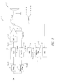
Figure 1 shows a block diagram of a first embodiment of the audio amplifier circuit of the present disclosure; -
Figure 2 shows a block diagram of a second embodiment of the audio amplifier circuit of the present disclosure; -
Figure 3 shows a block diagram of a possible embodiment of a block ofFigures 1 and2 according to the present disclosure; -
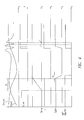
Figure 4 shows a plurality of charts showing the curve of the amplitude of various signals in the block ofFigure 3 , according to the present disclosure. - Referring to the accompanying figures, numeral 1 designates an audio amplifier, which is designed to provide an output signal Vout to an
audio transducer 2, such as a loudspeaker as is usually installed in a car. - Particularly, the audio amplifier circuit 1 comprises:
- an
audio power amplifier 3, preferably a switching or D class amplifier (although an AB class audio power amplifier may be also used), which is designed to receive an input audio signal Sin at its input, and is designed to generate the output signal Vout at its output, - a sensor 4 designed to detect an audible sound, such audible sound having at least one noise component Vn, to generate a detected signal Sdet at its output.
- It shall be first noted that the noise component Vn of the Sdet signal is the background or ambient noise as detected by the sensor 4.
- In other words, the sensor 4 is adapted to detect at least the background noise or ambient noise Vn when no audible sound Vs is emitted through the
acoustic transducer 2. - Conversely, if audible sounds Vs are also emitted by the
acoustic transducer 2, then the sensor 4 will generate the signal Sdet, which represents the sum of the contribution of background noise or ambient noise Vn and the contribution of audible sound Vs, i.e., the sensor 4 generates a signal Sdet equal to the sum of the signal for the audible sound Vs and the signal for the ambient noise Vn, i.e., Sdet=Vs+Vn. - In order to reduce the energy loss caused by power dissipation resulting from quiescent current through the idle channel of the
amplifier 3, theamplifier 3 has been advantageously designed to be off if the output signal Vout is zero or lower than a threshold value Vth. - The threshold value Vth is the minimum limit below which the user cannot hear sounds, whether these are background noise Vn or audible signals Vs.
- Particularly, the threshold value Vth is equal to a value that corresponds to a sound intensity of 10-12 W/m2.
- This affords the technical effect of switching off the channel of the
amplifier 3 that has a signal Vout lower (or zero) than the threshold value Vth, to achieve considerable power savings, and switching on theamplifier 3 as soon as the signal Vout becomes higher than Vth again. - It shall be noted that the audibility threshold value Vth may be expressed not only in terms of sound intensity, but also in equivalent terms of sound pressure, i.e., 0.000002 Pa or in terms of decibel, i.e., 0 dB.
- It should be noted that such switching on/off of the
amplifier 3, controlled by the signal Son/Soff, should occur without being perceived by the listener, which means that no impulsive noise that might affect listening quality should be generated during such transitions. - Furthermore, since a relatively high noise level may be present in the interior compartment of a car, due to tire rolling, engine noise and aerodynamic noise, the ambient noise component Vn is higher, and the minimum audibility threshold for the reproduced audio signal is also increased.
- In one aspect of the disclosure, there is the advantageous possibility of modulating the level of the reference signal Vth below which the
amplifier 3 can be switched off according to the ambient noise component Vn as detected by the sensor 4. - For this purpose, also referring to
Figures 1 and2 , it shall be noted that the circuit 1 comprises aprocessing block 5, which is designed to receive the detected signal Sdet at its input and to generate a switch-off signal Soff at its output, the latter signal being input to theaudio power amplifier 3. - Particularly, the
processing block 5 processes the detected signal Sdet according to the input signal Sin to identify the noise component Vn in the detected signal Sdet, to generate a reference signal Smod'. - If the input signal Sin is lower than the reference signal value Smod', then the
block 5 generates the switch-off signal Soff, to switch off the output channel of theamplifier 3 whose level is lower than the audible threshold value. - In other words, the signal Smod' represents the reference or threshold value below which no sound is audible by the listener.
- The
processing block 5 also generates a signal Sgain' at its output, the latter signal being input to thepower amplifier 3, to set the gain of thepower amplifier 3 to a minimum value. - In order to generate the reference signal Smod', the
processing block 5 may include anadaptive filter block 7, which is designed to filter said input signal Sin according to said detected signal Sdet, to generate a filtered signal Sfil. - The
adaptive filter block 7 is adapted to minimize the mean-square error of the signal Sdet according to the signal Sin. - The
adaptive filter 7 assumes that there is a strong correlation between the input signal Sin and the audible sound component Vs of the signal Sdet. - In other words, when the signal Sin is filtered by the
adaptive filter 7, the resulting signal is as close as possible to the signal component Vs of the signal Sdet, and hence subtraction of this signal from the signal Sdet provides the noise component Vn of the detected signal Sdet. - Therefore, the
adaptive filter 7 outputs the filtered signal Sfil, which represents the background or ambient noise component Vn only of such detected signal Sdet. - For instance, in a preferred embodiment, the
adaptive filter 7 consists of a Least Mean Square (LMS) filter. - Furthermore, in one embodiment, in order to generate the reference signal Smod', the audio amplifier circuit 1 may comprise a
delay block 8 which is designed to delay the input Sin by a predetermined interval of time to generate a delayed input signal at its output Sin,rit, which is advantageously input to thefilter block 7. - It shall be noted that the interval of time may be selected according to design specifications and is preset beforehand.
- Particularly, in a preferred embodiment, the adaptive filter operates with the delayed input signal Sin,rit and the detected signal Sdet at its input, to generate the filtered signal Sfil.
- This
processing block 5 may include anamplitude determining block 9, which is designed to receive the filtered signal Sfil at its input and generate a modulus signal Smod at its output representing the modulus of such filtered signal Sfil. - In other words, the signal Smod is representative of the amplitude value of said filtered signal Sfil, i.e., the amplitude value of the background or ambient noise component Vn of such detected signal Sdet.
- Furthermore, still in order to generate the reference signal Smod', in one embodiment the
processing block 5 may include an on/offblock 10, which is designed to receive the signal Smod at its input and is designed to generate the on/off signal Son/Soff and a signal gain Sgain at its output. - Particularly, to avoid the noise caused when switching on/off the
amplifier 3, the on/offblock 10 generates the off signal Soff at its output if, at least during a first period of time T1 ranging from 70 msec to 130 msec, preferably 100 msec, the value of the input signal Sin is lower than the value of the reference signal Smod'. - It shall be noted that, also for the signal Sgain', to avoid the noise caused when switching on/off the
amplifier 3, the minimum gain value for theamplifier 3 is reached within a time period T2 ranging from 10 msec to 30 msec, preferably 20 msec. - In other words, the signal Sgain' allows the gain of the
amplifier 3 to be set to its minimum value and to such minimum value to be reached within the period T2. - Particularly, to set the minimum gain of the
amplifier 3, in the preferred embodiment the signal Sgain' is obtained by again block 6. -
Such gain bock 6 receives a Sgain signal generated by the on/offblock 10 and the delayed input signal Sin,rit at its input, and generates the gain signal Sgain' that represents the actual gain value to be set in the amplifier, at its output. - In other words, in order to generate the signal Sgain', the
gain block 6 calculates the product of the signal Sin,rit and the signal Sgain, i.e., Sgain'= Sin,rit* Sgain. - It shall be noted that the audio amplifier circuit 1 may include a
weighting filter block 11 which is designed according to the sensitivity of a human ear. - The input signal Sin is input to the
weighting filter block 11 to generate a signal Sin,pes, which is in turn input to the on/offblock 10. - Particularly, in one aspect of the present disclosure, the on/off block 10 (or more generally the block 5) generates the off signal Soff if the input signal Sin,pes is lower than the value of the reference signal Smod'.
- Now, as soon as the
processing block 5 confirms that the input signal Sin,pes is lower than or equal to the reference signal Smod' during the time T1 and that the volume of theamplifier 3 is lowered to the minimum within the time T2 using the signal Sgain', theamplifier 3 may be switched off. - If the input signal Sin,pes is higher than the reference signal Smod', then the
amplifier 3 is immediately switched on using the signal Son, and the volume control is brought back to a zero attenuation value, or anyway to a working value, within an interval of time ranging from 7 msec to 13 msec, preferably of 10 msec. - The circuit 1 is obviously more easily controlled in a digital environment, and the switching
amplifier 3 may improve its behavior, because quick switching on/off is facilitated. - For this purpose, also referring to
Figures 1 and2 , the input signal Sin is preferably a digital signal, whereas the detected signal Sdet is converted into a digital form through an analog-to-digital conversion block (ADC) 20. - Furthermore, the signal Sgain' is converted to analog by a digital-to-analog converter (DAC) 21 before being input to the
amplifier 3. -
Figure 3 shows a possible embodiment of the on/offblock 10, andFigure 4 shows its operation with time. - As mentioned above, the on/off
block 10 has at its inputs the signal Smod and the input signal Sin or the version thereof that has been filtered by theweighting filter block 11 designed according to the sensitivity of a human ear, i.e., the signal Sin,pes. - Concerning the reference signal Smod', the latter is obtained by subtracting a predetermined constant quantity Q from the modulus signal Smod, i.e., the modulus noise component Vn of the signal Sdet.
- Particularly, a
summation node 12 is provided, which is designed to subtract the quantity Q, which is 20 dB in the diagram herein, from the modulus signal Smod, to generate the reference signal Smod'. - It shall be noted that the quantity Q represents the audibility threshold, below which the musical signal Vs cannot be heard.
- The signal Sin,pes is processed by an
effective value converter 13, to obtain a Root Mean Square (RMS) signal Sin, pes'. - A
comparator block 14 is designed to compare the two signals Sin,pes' and Smod' and to generate a Selab signal at its output. Particularly, if the signal Sin,pes' is higher than the signal Smod', then the output of thecomparator block 14, i.e., the signal Selab, is set to a high value. - The on/off
block 10 also includes atimer 15, a timer threshold block 15', aNAND gate 15", anintegration block 16, athreshold block 17, and aNOT gate 18. The output of thecomparator block 14 is coupled to respective inputs of thetimer 15 and theNOT gate 18. The output of thetimer 15 is coupled to the input of the timer threshold block 15' which has an output coupled to a first input of theNAND gate 15". The output of theNOT gate 18 is coupled to a second input of theNAND gate 15" which has an output coupled to an input of theintegration block 16. - Any transition from a low value to a high value of the signal Selab causes the NOT gate to transition to a low value, which causes the NAND gate to output a high value. In addition, the transition from low to high of the signal Selab causes the
timer 15 to be reset, which also causes the output of the timer threshold block 15' to be low. - When the signal Selab transitions from a high value to a low value of the signal Selab causes the
NOT gate 18 to output a high value and provides the start signal tosuch timer 15. The output of theNAND gate 15" will initially remain low high after to theNOT gate 18 transitions to the high value because the output of thetimer threshold block 15" continues to be low until the timer 15' output reaches the threshold of the timer threshold block. - From the start of the
timer 15, as soon as the preset threshold value of the period T1 (e.g., 100 msec) is exceeded, the timer threshold block 15'outputs a high value to the first input of theNAND gate 15", which causes the output signal y of the NAND gate to go to zero. This causes the attenuation step to be started by the signal Sgain', which is operative on the volume control of theamplifier 3 and brings it to the minimum within the period T2, i.e., within about 20 msec. - It shall be noted that, in one embodiment, the signal Sgain is obtained through the
integration block 16, which is designed to perform an integration of the signal y. - As soon as the volume of the
amplifier 3 reaches the minimum value, atthreshold block 17, theamplifier 3 may be switched off by generation of the signal Soff. - When the signal Sin,pes' rises again above the threshold Smod', the
timer 15 is reset, the signal y becomes immediately high again, theamplifier 3 is immediately switched on, and the volume control is brought to the minimum level to the working volume level within about 10msec. - Concerning the sensor 4, also referring to
Figure 2 , it is shown to comprise a microphone as generally used in the car-audio industry. - This microphone detects the audible signal component Vs and the noise component Vn to generate the detected signal Sdet at its output.
- It shall be noted that the signal Sdet is sent to the
processing block 5 through a dedicated connection. - Alternatively, since the presence of a microphone and relevant connections in the block diagram of
Figure 1 would cause an increase of the cost and complexity of the circuit 1, and since a dynamic loudspeaker is conceptually identical to a dynamic microphone, then a loudspeaker subjected to an acoustic pressure may be arranged to generate an electric signal. - In other words, if a dynamic loudspeaker is subjected to sound pressure, e.g., only the sound pressure generated by the background noise component Vn in the interior of the car or the sound pressure generated by the audible component Vs and the noise component Vn, then it generates a signal that is proportional to the sound pressure itself.
- The signal generated by such dynamic loudspeaker is equal to the detected signal Sdet from the microphone.
- It shall be noted that the existing connection of the
loudspeaker 2 to thepower amplifier 3 can transfer such signal Sdet to theamplifier 3, where the "microphone" signal may be detected, and the amplitude of the output signal may be accordingly controlled. - Therefore, it will be feasible to also utilize the
loudspeaker 2 as a microphone, thereby obtaining a low-cost circuit for reducing the absorbed current. - For this purpose, also particularly referring to
Figure 2 , the sensor 4 may include a voltage or current sensor, which is in signal communication with theaudio transducer 2 to detect the audible signal component Vs and/or the noise component Vs and generate the detected signal Sdet at its output. - Such voltage or current sensor is connected to the
ADC converter 20. - It shall be noted that, when the
amplifier 3 is operating, it is generally seen by thetransducer 2 as an ideal voltage generator. - This means that if the
transducer 2 connected thereto is subjected to a sound or acoustic pressure, it cannot change the output voltage of theamplifier 3, due to its non-zero output resistance. However, it will generate a current I having an ambient noise component In and/or an audible sound component Is, i.e., Sdet=I=Is+In. - In this case, such current I will be absorbed by the
amplifier 3 and, using known techniques, it may be transformed into voltage and applied to thefilter 7, possibly converted into digital by theADC converter 20. - On the other hand, the amplifier, in the off state, will generally behave as an open circuit. This means that if the
transducer 2 connected thereto is subjected to a sound or acoustic pressure, it cannot generate a current, unlike the previous case, but may generate a voltage V at the output of theamplifier 3. - The voltage V will represent the ambient noise component and/or the audible signal component Vn, i.e., V=Vs+Vn.
- In this case, the output voltage V of the
transducer 2 will be sent to thefilter 7 or possibly to the ADC converter. - A special control C from the on/off
block 10 will appropriately switch the operating mode of the current or voltage sensor that senses the acoustic signal Sdet detected by thetransducer 2, i.e., by the loudspeaker operating as a microphone. - The embodiment as shown with reference to
Figure 2 , affords low- or virtually zero-cost energy savings. - Average absorbed current savings are obviously a function of the type of audio program (spoken mode, music and music type) as well as the relevant level of listening volume and ambient noise.
- About 10% reduction of the average absorbed current is estimated, as compared with prior art circuits.
- Those skilled in the art will obviously appreciate that a number of changes and variants may be made to the arrangements as described hereinbefore to meet specific needs, without departure from the scope of the disclosure.
- The various embodiments described above can be combined to provide further embodiments. These and other changes can be made to the embodiments in light of the above-detailed description. In general, in the following claims, the terms used should not be construed to limit the claims to the specific embodiments disclosed in the specification and the claims, but should be construed to include all possible embodiments along with the full scope of equivalents to which such claims are entitled. Accordingly, the claims are not limited by the disclosure.
Claims (17)
- An audio amplifier circuit (1) designed to provide an output signal (Vout) to an audio transducer (2), said audio amplifier circuit (1) comprising:- an audio power amplifier (3) designed to receive an audio signal (Sin) at its input and designed to generate said output signal (Vout) at its output;- an audio sensor (4) designed to detect an audible sound, said audible sound having at least one noise component (Vn), said audio sensor (4) being designed to generate a detected signal (Sdet) at its output;characterized in that a processing block (5) which is designed to receive said detected signal (Sdet) at its input and to generate an off signal (Soff) at its output, the latter being located at the input of said audio power amplifier (3), said processing block (5) processing said detected signal (Sdet) according to said input signal (Sin) to identify said noise component (Vn) of said detected signal (Sdet) to generate a reference signal (Smod'), said processing block (5) generating said off signal (Soff) at its output when the value of said input signal (Sin) is lower than the value of said reference signal (Smod').
- An audio amplifier circuit as claimed in claim 1, wherein said processing block (5) generates said off signal (Soff) if, during at least a first period of time (T1) ranging from 70 msec to 130 msec, the value of said input signal Sin is lower than or equal to the value of said reference signal (Smod').
- An audio amplifier circuit as claimed in claim 1 or 2, wherein said processing block (5) comprises an adaptive filter block (7) which is designed to filter said input signal (Sin) according to said detected signal (Sdet), to minimize the mean-square error and generate said filtered signal (Sfil).
- An audio amplifier circuit as claimed in claim 3, wherein said processing block (5) comprises an amplitude determining block (9) designed to receive said filtered signal (Sfil) at its input and generate a modulus signal (Smod), wherein said determining block (9) is designed to generate said modulus signal (Smod) representative of the amplitude value of said filtered signal (Sfil).
- An audio amplifier circuit as claimed in claim 4, wherein said processing block (5) comprises an on/off block (10) which is designed to receive said modulus signal (Smod) at its input and is designed to generate said off signal (Soff) at its output, wherein said on/off block (10) processes said reference signal (Smod') by subtracting a quantity (Q) known beforehand from said modulus signal (Smod), said quantity (Q) representing an audibility threshold value.
- An audio amplifier circuit as claimed in claim 5, comprising a weighting filter block (11) conformed according to the sensitivity of a human ear, said input signal (sin) at the input of said on/off signal (10) being filtered by said weighting filter block (11), said off signal (Soff) being generated if the value of said input signal (Sin) is lower than the value of said reference signal (Smod').
- An audio amplifier circuit as claimed in claim 1, wherein said processing block (5) generates a first gain signal (Sgain') at its output, which is provided at the input of said audio power amplifier (3), to set the gain of said switching power amplifier (3) to a minimum value.
- An audio amplifier circuit as claimed in claim 7, wherein said first gain signal (Sgain') allows said power amplifier (3) to reach said minimum gain value within a second period of time (T2) ranging from 10 msec to 30 msec.
- An audio amplifier circuit as claimed in claim 5, comprising a gain block (6) which is designed to receive a second gain signal (Sgain) generated by said on/off block (10) and said input signal (Sin) at its input, and designed to generate said first gain signal (Sgain') at its output, said gain block (6) generating said first gain signal (Sgain'), by multiplying the input signal (Sin) by said second gain signal (Sgain).
- An audio amplifier circuit as claimed in claim 1, comprising a delay block (8) which is designed to receive said input signal (Sin) and to generate a delayed input signal (Sin,rit) at its output, said delay block delaying said input signal by a predetermined time.
- An audio amplifier circuit as claimed in claim 1, wherein said sensor (4) comprises a microphone for detecting said audible sound having at least said noise component and for generating said detected signal (Sdet) at its ouput, said microphone being in signal communication with said processing block (5).
- An audio amplifier circuit as claimed in claim 1, wherein said sensor (4) comprises a voltage or current sensor in signal communication with said audio transducer (2) and with said audio power amplifier (3) to detect said audible sound having at least said noise component and to generate said detected signal (Sdet) at its output, said voltage or current sensor being controlled to operate as a voltage sensor or current sensor in response to a control (C) generated by said processing block (5).
- An audio amplifier circuit as claimed in claim 1, wherein said processing block comprises an Analog-to-Digital Converter block (ADC), said detected signal (Sdet) being converted into digital by said Analog-to-Digital converter block.
- A method of optimizing the efficiency of an audio amplifier circuit (1) designed to provide an output signal (Vout) to an audio transducer (2), said method comprising the steps of:- providing a power amplifier (3) designed to receive an audio signal (Sin) at its input and designed to generate said output signal (Vout) at its output,- providing a sensor (4) designed to detect an audible sound having at least one noise component (Vn), to generate a detected signal (Sdet) at its output, characterized in that it comprises the steps of:- processing said detected signal (Sdet) according to said input signal (Sin) to identify said noise component (Vn) of said detected signal (Sdet) and generate a reference signal (Smod') and- generating said off signal (Soff) at its output, if the value of said input signal (Sin) is lower than the value of said reference signal (Smod').
- A method of optimizing the efficiency of an audio amplifier circuit (1) as claimed in claim 14, wherein said step of generating said off signal (Soff) is carried out if, at least during a first period of time (T1) ranging from 70 msec to 130 msec, the value of said input signal (Sin) is lower than the value of said reference signal (Smod').
- A method of optimizing the efficiency of an audio amplifier circuit (1) as claimed in claim 14, comprising the additional step of generating a gain signal (Sgain'), the latter being provided at the input of said switching power amplifier (3), to set the gain of said power amplifier (3) to a minimum value.
- A method of optimizing the efficiency of an audio amplifier circuit (1) as claimed in claim 16, wherein said step of generating said gain signal (Sgain') comprises the additional step of reaching said minimum gain value within a second period of time (T2) ranging from 10 msec to 30 msec.
Applications Claiming Priority (1)
| Application Number | Priority Date | Filing Date | Title |
|---|---|---|---|
| IT000985A ITMI20110985A1 (en) | 2011-05-31 | 2011-05-31 | AUDIO AMPLIFIER CIRCUIT AND ITS OPERATING METHOD. |
Publications (2)
| Publication Number | Publication Date |
|---|---|
| EP2530831A1 true EP2530831A1 (en) | 2012-12-05 |
| EP2530831B1 EP2530831B1 (en) | 2018-04-11 |
Family
ID=44554793
Family Applications (1)
| Application Number | Title | Priority Date | Filing Date |
|---|---|---|---|
| EP12169862.5A Active EP2530831B1 (en) | 2011-05-31 | 2012-05-29 | Audio amplifier circuit and method of operation thereof |
Country Status (3)
| Country | Link |
|---|---|
| US (1) | US9008322B2 (en) |
| EP (1) | EP2530831B1 (en) |
| IT (1) | ITMI20110985A1 (en) |
Cited By (2)
| Publication number | Priority date | Publication date | Assignee | Title |
|---|---|---|---|---|
| CN103281654A (en) * | 2013-04-16 | 2013-09-04 | 深圳市泰金田科技有限公司 | Method and device for increasing amplifier power utilization rate by compensating crest power with trough power |
| CN104967945A (en) * | 2015-06-03 | 2015-10-07 | 广东欧珀移动通信有限公司 | A headphone power amplifier and a control method for the headphone power amplifier |
Families Citing this family (6)
| Publication number | Priority date | Publication date | Assignee | Title |
|---|---|---|---|---|
| EP2850611B1 (en) | 2012-06-10 | 2019-08-21 | Nuance Communications, Inc. | Noise dependent signal processing for in-car communication systems with multiple acoustic zones |
| EP2859772B1 (en) * | 2012-06-10 | 2018-12-19 | Nuance Communications, Inc. | Wind noise detection for in-car communication systems with multiple acoustic zones |
| KR101855725B1 (en) | 2014-01-13 | 2018-06-20 | 삼성전자주식회사 | Audio Outputting Control Method and Electronic Device supporting the same |
| US10569115B2 (en) | 2014-11-24 | 2020-02-25 | Force Sv, Llc | Methods and systems for disrupting phenomena with waves |
| US12347414B2 (en) * | 2019-04-10 | 2025-07-01 | Haoze GAO | Method, apparatus, and systems for fire suppression using sound waves |
| CN112312280B (en) * | 2019-07-31 | 2022-03-01 | 北京地平线机器人技术研发有限公司 | In-vehicle sound playing method and device |
Citations (3)
| Publication number | Priority date | Publication date | Assignee | Title |
|---|---|---|---|---|
| US3934085A (en) * | 1973-03-28 | 1976-01-20 | Television Research Limited | Audio amplifier systems |
| JPH08242124A (en) * | 1995-03-01 | 1996-09-17 | Kokusai Electric Co Ltd | Low power consumption type amplifier |
| US20050190927A1 (en) * | 2004-02-27 | 2005-09-01 | Prn Corporation | Speaker systems and methods having amplitude and frequency response compensation |
Family Cites Families (8)
| Publication number | Priority date | Publication date | Assignee | Title |
|---|---|---|---|---|
| JP3306600B2 (en) * | 1992-08-05 | 2002-07-24 | 三菱電機株式会社 | Automatic volume control |
| US5907622A (en) * | 1995-09-21 | 1999-05-25 | Dougherty; A. Michael | Automatic noise compensation system for audio reproduction equipment |
| US5822598A (en) * | 1996-07-12 | 1998-10-13 | Ast Research, Inc. | Audio activity detection circuit to increase battery life in portable computers |
| US6785392B1 (en) * | 2000-04-25 | 2004-08-31 | Tripath Technology, Inc. | Methods and apparatus for enabling or disabling an amplifier |
| US7394312B2 (en) * | 2004-11-15 | 2008-07-01 | Pioneer Corporation | Re-configurable amplifier protection apparatus and method |
| JP5003419B2 (en) * | 2007-11-09 | 2012-08-15 | ヤマハ株式会社 | Sound processing apparatus and program |
| JP4810711B2 (en) * | 2010-01-14 | 2011-11-09 | オンキヨー株式会社 | Amplification equipment |
| US20120275624A1 (en) * | 2011-04-28 | 2012-11-01 | Szuyu Ho | Energy-saving audio-amplifier control device |
-
2011
- 2011-05-31 IT IT000985A patent/ITMI20110985A1/en unknown
-
2012
- 2012-05-29 EP EP12169862.5A patent/EP2530831B1/en active Active
- 2012-05-30 US US13/484,085 patent/US9008322B2/en active Active
Patent Citations (3)
| Publication number | Priority date | Publication date | Assignee | Title |
|---|---|---|---|---|
| US3934085A (en) * | 1973-03-28 | 1976-01-20 | Television Research Limited | Audio amplifier systems |
| JPH08242124A (en) * | 1995-03-01 | 1996-09-17 | Kokusai Electric Co Ltd | Low power consumption type amplifier |
| US20050190927A1 (en) * | 2004-02-27 | 2005-09-01 | Prn Corporation | Speaker systems and methods having amplitude and frequency response compensation |
Cited By (2)
| Publication number | Priority date | Publication date | Assignee | Title |
|---|---|---|---|---|
| CN103281654A (en) * | 2013-04-16 | 2013-09-04 | 深圳市泰金田科技有限公司 | Method and device for increasing amplifier power utilization rate by compensating crest power with trough power |
| CN104967945A (en) * | 2015-06-03 | 2015-10-07 | 广东欧珀移动通信有限公司 | A headphone power amplifier and a control method for the headphone power amplifier |
Also Published As
| Publication number | Publication date |
|---|---|
| ITMI20110985A1 (en) | 2012-12-01 |
| EP2530831B1 (en) | 2018-04-11 |
| US9008322B2 (en) | 2015-04-14 |
| US20120308050A1 (en) | 2012-12-06 |
Similar Documents
| Publication | Publication Date | Title |
|---|---|---|
| US9008322B2 (en) | Efficiency optimizer of an audio power amplifier for car radio | |
| US9607628B2 (en) | Audio system | |
| US8831934B2 (en) | Speech enhancement method and system | |
| EP1110306B1 (en) | Methods for adjusting audio signals responsive to changes in a power supply level and related communications devices | |
| US8306238B2 (en) | Method and circuit for controlling an output of an audio signal of a battery-powered device | |
| JP5982864B2 (en) | Audio amplifier | |
| CN102656799A (en) | Circuit and method for reducing noise in class D amplifiers | |
| US20120257770A1 (en) | Method and apparatus to supply power voltage to a mobile device in a variable manner | |
| TW201739268A (en) | Hand-held electronic apparatus, sound producing system and control method of sound producing thereof | |
| JP2005339355A (en) | Power supply control apparatus and power supply circuit control method | |
| US8705758B2 (en) | Audio processing device and method for reducing echo from a second signal in a first signal | |
| US10979010B2 (en) | Audio signal processing | |
| CN112260653A (en) | Low-power consumption instant-use constant-voltage power amplifier system controlled by DSP | |
| US11108365B2 (en) | Class-D amplifier and operating method | |
| CN113661652A (en) | Audio signal processing method, related device, audio equipment, and storage medium | |
| US9543908B2 (en) | Adaptive rail voltage regulation on power supplies | |
| CN102857182A (en) | Gain control device of multimedia equipment | |
| JP2008219713A (en) | Noise canceling headphones | |
| US8618403B2 (en) | Tone control apparatus | |
| Chen et al. | A 2.5 W tablet speaker delivering 3.2 W pseudo high power by psychoacoustic model based adaptive power management system | |
| KR100284188B1 (en) | Voice signal amplification device | |
| JPH03119899A (en) | Superdirective loudspeaker unit | |
| TW201536061A (en) | Power management system and method thereof | |
| US20050141732A1 (en) | Amplifying apparatus | |
| KR20190042390A (en) | Apparatus for amplifying sound signal in multi level and method thereof |
Legal Events
| Date | Code | Title | Description |
|---|---|---|---|
| PUAI | Public reference made under article 153(3) epc to a published international application that has entered the european phase |
Free format text: ORIGINAL CODE: 0009012 |
|
| AK | Designated contracting states |
Kind code of ref document: A1 Designated state(s): AL AT BE BG CH CY CZ DE DK EE ES FI FR GB GR HR HU IE IS IT LI LT LU LV MC MK MT NL NO PL PT RO RS SE SI SK SM TR |
|
| AX | Request for extension of the european patent |
Extension state: BA ME |
|
| 17P | Request for examination filed |
Effective date: 20130522 |
|
| 17Q | First examination report despatched |
Effective date: 20170130 |
|
| GRAP | Despatch of communication of intention to grant a patent |
Free format text: ORIGINAL CODE: EPIDOSNIGR1 |
|
| INTG | Intention to grant announced |
Effective date: 20170628 |
|
| GRAJ | Information related to disapproval of communication of intention to grant by the applicant or resumption of examination proceedings by the epo deleted |
Free format text: ORIGINAL CODE: EPIDOSDIGR1 |
|
| GRAP | Despatch of communication of intention to grant a patent |
Free format text: ORIGINAL CODE: EPIDOSNIGR1 |
|
| INTC | Intention to grant announced (deleted) | ||
| INTG | Intention to grant announced |
Effective date: 20171110 |
|
| GRAS | Grant fee paid |
Free format text: ORIGINAL CODE: EPIDOSNIGR3 |
|
| GRAA | (expected) grant |
Free format text: ORIGINAL CODE: 0009210 |
|
| AK | Designated contracting states |
Kind code of ref document: B1 Designated state(s): AL AT BE BG CH CY CZ DE DK EE ES FI FR GB GR HR HU IE IS IT LI LT LU LV MC MK MT NL NO PL PT RO RS SE SI SK SM TR |
|
| REG | Reference to a national code |
Ref country code: GB Ref legal event code: FG4D |
|
| REG | Reference to a national code |
Ref country code: CH Ref legal event code: EP |
|
| REG | Reference to a national code |
Ref country code: AT Ref legal event code: REF Ref document number: 989047 Country of ref document: AT Kind code of ref document: T Effective date: 20180415 |
|
| REG | Reference to a national code |
Ref country code: IE Ref legal event code: FG4D |
|
| REG | Reference to a national code |
Ref country code: DE Ref legal event code: R096 Ref document number: 602012044966 Country of ref document: DE |
|
| REG | Reference to a national code |
Ref country code: FR Ref legal event code: PLFP Year of fee payment: 7 |
|
| REG | Reference to a national code |
Ref country code: NL Ref legal event code: MP Effective date: 20180411 |
|
| REG | Reference to a national code |
Ref country code: LT Ref legal event code: MG4D |
|
| PG25 | Lapsed in a contracting state [announced via postgrant information from national office to epo] |
Ref country code: NL Free format text: LAPSE BECAUSE OF FAILURE TO SUBMIT A TRANSLATION OF THE DESCRIPTION OR TO PAY THE FEE WITHIN THE PRESCRIBED TIME-LIMIT Effective date: 20180411 |
|
| PG25 | Lapsed in a contracting state [announced via postgrant information from national office to epo] |
Ref country code: LT Free format text: LAPSE BECAUSE OF FAILURE TO SUBMIT A TRANSLATION OF THE DESCRIPTION OR TO PAY THE FEE WITHIN THE PRESCRIBED TIME-LIMIT Effective date: 20180411 Ref country code: PL Free format text: LAPSE BECAUSE OF FAILURE TO SUBMIT A TRANSLATION OF THE DESCRIPTION OR TO PAY THE FEE WITHIN THE PRESCRIBED TIME-LIMIT Effective date: 20180411 Ref country code: ES Free format text: LAPSE BECAUSE OF FAILURE TO SUBMIT A TRANSLATION OF THE DESCRIPTION OR TO PAY THE FEE WITHIN THE PRESCRIBED TIME-LIMIT Effective date: 20180411 Ref country code: BG Free format text: LAPSE BECAUSE OF FAILURE TO SUBMIT A TRANSLATION OF THE DESCRIPTION OR TO PAY THE FEE WITHIN THE PRESCRIBED TIME-LIMIT Effective date: 20180711 Ref country code: AL Free format text: LAPSE BECAUSE OF FAILURE TO SUBMIT A TRANSLATION OF THE DESCRIPTION OR TO PAY THE FEE WITHIN THE PRESCRIBED TIME-LIMIT Effective date: 20180411 Ref country code: FI Free format text: LAPSE BECAUSE OF FAILURE TO SUBMIT A TRANSLATION OF THE DESCRIPTION OR TO PAY THE FEE WITHIN THE PRESCRIBED TIME-LIMIT Effective date: 20180411 Ref country code: NO Free format text: LAPSE BECAUSE OF FAILURE TO SUBMIT A TRANSLATION OF THE DESCRIPTION OR TO PAY THE FEE WITHIN THE PRESCRIBED TIME-LIMIT Effective date: 20180711 Ref country code: SE Free format text: LAPSE BECAUSE OF FAILURE TO SUBMIT A TRANSLATION OF THE DESCRIPTION OR TO PAY THE FEE WITHIN THE PRESCRIBED TIME-LIMIT Effective date: 20180411 |
|
| PG25 | Lapsed in a contracting state [announced via postgrant information from national office to epo] |
Ref country code: GR Free format text: LAPSE BECAUSE OF FAILURE TO SUBMIT A TRANSLATION OF THE DESCRIPTION OR TO PAY THE FEE WITHIN THE PRESCRIBED TIME-LIMIT Effective date: 20180712 Ref country code: LV Free format text: LAPSE BECAUSE OF FAILURE TO SUBMIT A TRANSLATION OF THE DESCRIPTION OR TO PAY THE FEE WITHIN THE PRESCRIBED TIME-LIMIT Effective date: 20180411 Ref country code: RS Free format text: LAPSE BECAUSE OF FAILURE TO SUBMIT A TRANSLATION OF THE DESCRIPTION OR TO PAY THE FEE WITHIN THE PRESCRIBED TIME-LIMIT Effective date: 20180411 Ref country code: HR Free format text: LAPSE BECAUSE OF FAILURE TO SUBMIT A TRANSLATION OF THE DESCRIPTION OR TO PAY THE FEE WITHIN THE PRESCRIBED TIME-LIMIT Effective date: 20180411 |
|
| REG | Reference to a national code |
Ref country code: CH Ref legal event code: PL |
|
| REG | Reference to a national code |
Ref country code: AT Ref legal event code: MK05 Ref document number: 989047 Country of ref document: AT Kind code of ref document: T Effective date: 20180411 |
|
| PG25 | Lapsed in a contracting state [announced via postgrant information from national office to epo] |
Ref country code: PT Free format text: LAPSE BECAUSE OF FAILURE TO SUBMIT A TRANSLATION OF THE DESCRIPTION OR TO PAY THE FEE WITHIN THE PRESCRIBED TIME-LIMIT Effective date: 20180813 |
|
| REG | Reference to a national code |
Ref country code: DE Ref legal event code: R097 Ref document number: 602012044966 Country of ref document: DE |
|
| REG | Reference to a national code |
Ref country code: BE Ref legal event code: MM Effective date: 20180531 |
|
| PG25 | Lapsed in a contracting state [announced via postgrant information from national office to epo] |
Ref country code: MC Free format text: LAPSE BECAUSE OF FAILURE TO SUBMIT A TRANSLATION OF THE DESCRIPTION OR TO PAY THE FEE WITHIN THE PRESCRIBED TIME-LIMIT Effective date: 20180411 Ref country code: CZ Free format text: LAPSE BECAUSE OF FAILURE TO SUBMIT A TRANSLATION OF THE DESCRIPTION OR TO PAY THE FEE WITHIN THE PRESCRIBED TIME-LIMIT Effective date: 20180411 Ref country code: SK Free format text: LAPSE BECAUSE OF FAILURE TO SUBMIT A TRANSLATION OF THE DESCRIPTION OR TO PAY THE FEE WITHIN THE PRESCRIBED TIME-LIMIT Effective date: 20180411 Ref country code: RO Free format text: LAPSE BECAUSE OF FAILURE TO SUBMIT A TRANSLATION OF THE DESCRIPTION OR TO PAY THE FEE WITHIN THE PRESCRIBED TIME-LIMIT Effective date: 20180411 Ref country code: DK Free format text: LAPSE BECAUSE OF FAILURE TO SUBMIT A TRANSLATION OF THE DESCRIPTION OR TO PAY THE FEE WITHIN THE PRESCRIBED TIME-LIMIT Effective date: 20180411 Ref country code: AT Free format text: LAPSE BECAUSE OF FAILURE TO SUBMIT A TRANSLATION OF THE DESCRIPTION OR TO PAY THE FEE WITHIN THE PRESCRIBED TIME-LIMIT Effective date: 20180411 Ref country code: EE Free format text: LAPSE BECAUSE OF FAILURE TO SUBMIT A TRANSLATION OF THE DESCRIPTION OR TO PAY THE FEE WITHIN THE PRESCRIBED TIME-LIMIT Effective date: 20180411 |
|
| PLBE | No opposition filed within time limit |
Free format text: ORIGINAL CODE: 0009261 |
|
| STAA | Information on the status of an ep patent application or granted ep patent |
Free format text: STATUS: NO OPPOSITION FILED WITHIN TIME LIMIT |
|
| REG | Reference to a national code |
Ref country code: IE Ref legal event code: MM4A |
|
| PG25 | Lapsed in a contracting state [announced via postgrant information from national office to epo] |
Ref country code: CH Free format text: LAPSE BECAUSE OF NON-PAYMENT OF DUE FEES Effective date: 20180531 Ref country code: SM Free format text: LAPSE BECAUSE OF FAILURE TO SUBMIT A TRANSLATION OF THE DESCRIPTION OR TO PAY THE FEE WITHIN THE PRESCRIBED TIME-LIMIT Effective date: 20180411 Ref country code: LI Free format text: LAPSE BECAUSE OF NON-PAYMENT OF DUE FEES Effective date: 20180531 Ref country code: IT Free format text: LAPSE BECAUSE OF FAILURE TO SUBMIT A TRANSLATION OF THE DESCRIPTION OR TO PAY THE FEE WITHIN THE PRESCRIBED TIME-LIMIT Effective date: 20180411 |
|
| 26N | No opposition filed |
Effective date: 20190114 |
|
| GBPC | Gb: european patent ceased through non-payment of renewal fee |
Effective date: 20180711 |
|
| PG25 | Lapsed in a contracting state [announced via postgrant information from national office to epo] |
Ref country code: LU Free format text: LAPSE BECAUSE OF NON-PAYMENT OF DUE FEES Effective date: 20180529 |
|
| PG25 | Lapsed in a contracting state [announced via postgrant information from national office to epo] |
Ref country code: IE Free format text: LAPSE BECAUSE OF NON-PAYMENT OF DUE FEES Effective date: 20180529 Ref country code: GB Free format text: LAPSE BECAUSE OF NON-PAYMENT OF DUE FEES Effective date: 20180711 |
|
| PG25 | Lapsed in a contracting state [announced via postgrant information from national office to epo] |
Ref country code: SI Free format text: LAPSE BECAUSE OF FAILURE TO SUBMIT A TRANSLATION OF THE DESCRIPTION OR TO PAY THE FEE WITHIN THE PRESCRIBED TIME-LIMIT Effective date: 20180411 Ref country code: BE Free format text: LAPSE BECAUSE OF NON-PAYMENT OF DUE FEES Effective date: 20180531 |
|
| PG25 | Lapsed in a contracting state [announced via postgrant information from national office to epo] |
Ref country code: MT Free format text: LAPSE BECAUSE OF NON-PAYMENT OF DUE FEES Effective date: 20180529 |
|
| PG25 | Lapsed in a contracting state [announced via postgrant information from national office to epo] |
Ref country code: TR Free format text: LAPSE BECAUSE OF FAILURE TO SUBMIT A TRANSLATION OF THE DESCRIPTION OR TO PAY THE FEE WITHIN THE PRESCRIBED TIME-LIMIT Effective date: 20180411 |
|
| PG25 | Lapsed in a contracting state [announced via postgrant information from national office to epo] |
Ref country code: HU Free format text: LAPSE BECAUSE OF FAILURE TO SUBMIT A TRANSLATION OF THE DESCRIPTION OR TO PAY THE FEE WITHIN THE PRESCRIBED TIME-LIMIT; INVALID AB INITIO Effective date: 20120529 |
|
| PG25 | Lapsed in a contracting state [announced via postgrant information from national office to epo] |
Ref country code: MK Free format text: LAPSE BECAUSE OF NON-PAYMENT OF DUE FEES Effective date: 20180411 Ref country code: CY Free format text: LAPSE BECAUSE OF FAILURE TO SUBMIT A TRANSLATION OF THE DESCRIPTION OR TO PAY THE FEE WITHIN THE PRESCRIBED TIME-LIMIT Effective date: 20180411 |
|
| PG25 | Lapsed in a contracting state [announced via postgrant information from national office to epo] |
Ref country code: IS Free format text: LAPSE BECAUSE OF FAILURE TO SUBMIT A TRANSLATION OF THE DESCRIPTION OR TO PAY THE FEE WITHIN THE PRESCRIBED TIME-LIMIT Effective date: 20180811 |
|
| PGFP | Annual fee paid to national office [announced via postgrant information from national office to epo] |
Ref country code: FR Payment date: 20200422 Year of fee payment: 9 |
|
| PG25 | Lapsed in a contracting state [announced via postgrant information from national office to epo] |
Ref country code: FR Free format text: LAPSE BECAUSE OF NON-PAYMENT OF DUE FEES Effective date: 20210531 |
|
| PGFP | Annual fee paid to national office [announced via postgrant information from national office to epo] |
Ref country code: DE Payment date: 20250423 Year of fee payment: 14 |