EP2530734A1 - Solar cell module and manufacturing method of same - Google Patents
Solar cell module and manufacturing method of same Download PDFInfo
- Publication number
- EP2530734A1 EP2530734A1 EP11737034A EP11737034A EP2530734A1 EP 2530734 A1 EP2530734 A1 EP 2530734A1 EP 11737034 A EP11737034 A EP 11737034A EP 11737034 A EP11737034 A EP 11737034A EP 2530734 A1 EP2530734 A1 EP 2530734A1
- Authority
- EP
- European Patent Office
- Prior art keywords
- solar cell
- wiring member
- resin adhesive
- conductive particles
- conductive
- Prior art date
- Legal status (The legal status is an assumption and is not a legal conclusion. Google has not performed a legal analysis and makes no representation as to the accuracy of the status listed.)
- Withdrawn
Links
- 238000004519 manufacturing process Methods 0.000 title claims description 22
- 229920005989 resin Polymers 0.000 claims abstract description 208
- 239000011347 resin Substances 0.000 claims abstract description 208
- 239000002245 particle Substances 0.000 claims abstract description 192
- 239000000853 adhesive Substances 0.000 claims abstract description 174
- 230000001070 adhesive effect Effects 0.000 claims abstract description 174
- 229910052751 metal Inorganic materials 0.000 claims abstract description 17
- 239000002184 metal Substances 0.000 claims abstract description 17
- 239000011888 foil Substances 0.000 claims abstract description 9
- 238000004026 adhesive bonding Methods 0.000 claims description 16
- 238000005520 cutting process Methods 0.000 claims description 14
- 238000012360 testing method Methods 0.000 description 14
- 230000007423 decrease Effects 0.000 description 9
- 239000004065 semiconductor Substances 0.000 description 6
- 229910000679 solder Inorganic materials 0.000 description 6
- 229910052782 aluminium Inorganic materials 0.000 description 5
- XAGFODPZIPBFFR-UHFFFAOYSA-N aluminium Chemical compound [Al] XAGFODPZIPBFFR-UHFFFAOYSA-N 0.000 description 5
- 238000006243 chemical reaction Methods 0.000 description 5
- 238000000034 method Methods 0.000 description 5
- 229910045601 alloy Inorganic materials 0.000 description 4
- 239000000956 alloy Substances 0.000 description 4
- 239000005038 ethylene vinyl acetate Substances 0.000 description 4
- 238000011156 evaluation Methods 0.000 description 4
- 239000011521 glass Substances 0.000 description 4
- 239000000463 material Substances 0.000 description 4
- 239000000203 mixture Substances 0.000 description 4
- 229920001200 poly(ethylene-vinyl acetate) Polymers 0.000 description 4
- 239000000565 sealant Substances 0.000 description 4
- PXHVJJICTQNCMI-UHFFFAOYSA-N Nickel Chemical compound [Ni] PXHVJJICTQNCMI-UHFFFAOYSA-N 0.000 description 3
- 239000003795 chemical substances by application Substances 0.000 description 3
- 239000011248 coating agent Substances 0.000 description 3
- 238000000576 coating method Methods 0.000 description 3
- 239000003822 epoxy resin Substances 0.000 description 3
- 229910052809 inorganic oxide Inorganic materials 0.000 description 3
- 229920000647 polyepoxide Polymers 0.000 description 3
- 229910052709 silver Inorganic materials 0.000 description 3
- 239000004332 silver Substances 0.000 description 3
- 229920001187 thermosetting polymer Polymers 0.000 description 3
- KXGFMDJXCMQABM-UHFFFAOYSA-N 2-methoxy-6-methylphenol Chemical compound [CH]OC1=CC=CC([CH])=C1O KXGFMDJXCMQABM-UHFFFAOYSA-N 0.000 description 2
- 239000004925 Acrylic resin Substances 0.000 description 2
- 229920000178 Acrylic resin Polymers 0.000 description 2
- RYGMFSIKBFXOCR-UHFFFAOYSA-N Copper Chemical compound [Cu] RYGMFSIKBFXOCR-UHFFFAOYSA-N 0.000 description 2
- 239000004593 Epoxy Substances 0.000 description 2
- VYPSYNLAJGMNEJ-UHFFFAOYSA-N Silicium dioxide Chemical compound O=[Si]=O VYPSYNLAJGMNEJ-UHFFFAOYSA-N 0.000 description 2
- 239000000969 carrier Substances 0.000 description 2
- 229920001577 copolymer Polymers 0.000 description 2
- 229910021419 crystalline silicon Inorganic materials 0.000 description 2
- 230000000694 effects Effects 0.000 description 2
- 238000010438 heat treatment Methods 0.000 description 2
- 150000002739 metals Chemical class 0.000 description 2
- 229920001568 phenolic resin Polymers 0.000 description 2
- 239000005011 phenolic resin Substances 0.000 description 2
- 229920002037 poly(vinyl butyral) polymer Polymers 0.000 description 2
- 229920001721 polyimide Polymers 0.000 description 2
- 239000009719 polyimide resin Substances 0.000 description 2
- 238000007650 screen-printing Methods 0.000 description 2
- 229920002050 silicone resin Polymers 0.000 description 2
- 229920002803 thermoplastic polyurethane Polymers 0.000 description 2
- 229910017944 Ag—Cu Inorganic materials 0.000 description 1
- 229910001218 Gallium arsenide Inorganic materials 0.000 description 1
- BQCADISMDOOEFD-UHFFFAOYSA-N Silver Chemical compound [Ag] BQCADISMDOOEFD-UHFFFAOYSA-N 0.000 description 1
- ATJFFYVFTNAWJD-UHFFFAOYSA-N Tin Chemical compound [Sn] ATJFFYVFTNAWJD-UHFFFAOYSA-N 0.000 description 1
- GWEVSGVZZGPLCZ-UHFFFAOYSA-N Titan oxide Chemical compound O=[Ti]=O GWEVSGVZZGPLCZ-UHFFFAOYSA-N 0.000 description 1
- PNEYBMLMFCGWSK-UHFFFAOYSA-N aluminium oxide Inorganic materials [O-2].[O-2].[O-2].[Al+3].[Al+3] PNEYBMLMFCGWSK-UHFFFAOYSA-N 0.000 description 1
- 229910021417 amorphous silicon Inorganic materials 0.000 description 1
- 239000012298 atmosphere Substances 0.000 description 1
- 239000011230 binding agent Substances 0.000 description 1
- 150000001875 compounds Chemical class 0.000 description 1
- 238000001816 cooling Methods 0.000 description 1
- 229910052802 copper Inorganic materials 0.000 description 1
- 239000010949 copper Substances 0.000 description 1
- 239000011889 copper foil Substances 0.000 description 1
- 238000009826 distribution Methods 0.000 description 1
- 238000002474 experimental method Methods 0.000 description 1
- 239000000945 filler Substances 0.000 description 1
- PCHJSUWPFVWCPO-UHFFFAOYSA-N gold Chemical compound [Au] PCHJSUWPFVWCPO-UHFFFAOYSA-N 0.000 description 1
- 229910052737 gold Inorganic materials 0.000 description 1
- 239000010931 gold Substances 0.000 description 1
- 238000005259 measurement Methods 0.000 description 1
- 229910052759 nickel Inorganic materials 0.000 description 1
- 229910021420 polycrystalline silicon Inorganic materials 0.000 description 1
- 239000000843 powder Substances 0.000 description 1
- 238000003825 pressing Methods 0.000 description 1
- 238000007789 sealing Methods 0.000 description 1
- 239000000377 silicon dioxide Substances 0.000 description 1
- 238000005245 sintering Methods 0.000 description 1
- 230000003746 surface roughness Effects 0.000 description 1
- 229910052718 tin Inorganic materials 0.000 description 1
- OGIDPMRJRNCKJF-UHFFFAOYSA-N titanium oxide Inorganic materials [Ti]=O OGIDPMRJRNCKJF-UHFFFAOYSA-N 0.000 description 1
- 238000011179 visual inspection Methods 0.000 description 1
Images
Classifications
-
- H—ELECTRICITY
- H10—SEMICONDUCTOR DEVICES; ELECTRIC SOLID-STATE DEVICES NOT OTHERWISE PROVIDED FOR
- H10F—INORGANIC SEMICONDUCTOR DEVICES SENSITIVE TO INFRARED RADIATION, LIGHT, ELECTROMAGNETIC RADIATION OF SHORTER WAVELENGTH OR CORPUSCULAR RADIATION
- H10F71/00—Manufacture or treatment of devices covered by this subclass
- H10F71/137—Batch treatment of the devices
- H10F71/1375—Apparatus for automatic interconnection of photovoltaic cells in a module
-
- H—ELECTRICITY
- H10—SEMICONDUCTOR DEVICES; ELECTRIC SOLID-STATE DEVICES NOT OTHERWISE PROVIDED FOR
- H10F—INORGANIC SEMICONDUCTOR DEVICES SENSITIVE TO INFRARED RADIATION, LIGHT, ELECTROMAGNETIC RADIATION OF SHORTER WAVELENGTH OR CORPUSCULAR RADIATION
- H10F19/00—Integrated devices, or assemblies of multiple devices, comprising at least one photovoltaic cell covered by group H10F10/00, e.g. photovoltaic modules
- H10F19/80—Encapsulations or containers for integrated devices, or assemblies of multiple devices, having photovoltaic cells
- H10F19/804—Materials of encapsulations
-
- H—ELECTRICITY
- H10—SEMICONDUCTOR DEVICES; ELECTRIC SOLID-STATE DEVICES NOT OTHERWISE PROVIDED FOR
- H10F—INORGANIC SEMICONDUCTOR DEVICES SENSITIVE TO INFRARED RADIATION, LIGHT, ELECTROMAGNETIC RADIATION OF SHORTER WAVELENGTH OR CORPUSCULAR RADIATION
- H10F19/00—Integrated devices, or assemblies of multiple devices, comprising at least one photovoltaic cell covered by group H10F10/00, e.g. photovoltaic modules
- H10F19/90—Structures for connecting between photovoltaic cells, e.g. interconnections or insulating spacers
- H10F19/902—Structures for connecting between photovoltaic cells, e.g. interconnections or insulating spacers for series or parallel connection of photovoltaic cells
- H10F19/906—Structures for connecting between photovoltaic cells, e.g. interconnections or insulating spacers for series or parallel connection of photovoltaic cells characterised by the materials of the structures
-
- Y—GENERAL TAGGING OF NEW TECHNOLOGICAL DEVELOPMENTS; GENERAL TAGGING OF CROSS-SECTIONAL TECHNOLOGIES SPANNING OVER SEVERAL SECTIONS OF THE IPC; TECHNICAL SUBJECTS COVERED BY FORMER USPC CROSS-REFERENCE ART COLLECTIONS [XRACs] AND DIGESTS
- Y02—TECHNOLOGIES OR APPLICATIONS FOR MITIGATION OR ADAPTATION AGAINST CLIMATE CHANGE
- Y02E—REDUCTION OF GREENHOUSE GAS [GHG] EMISSIONS, RELATED TO ENERGY GENERATION, TRANSMISSION OR DISTRIBUTION
- Y02E10/00—Energy generation through renewable energy sources
- Y02E10/50—Photovoltaic [PV] energy
Definitions
- This invention relates to a solar cell module and a manufacturing method of the same. Particularly, this invention relates to a solar cell module including a plurality of solar cells electrically connected to one another using wiring members, and a manufacturing method of the same.
- a solar cell module typically includes a plurality of solar cells.
- the solar cells are electrically connected to one another in series or in parallel using wiring members.
- solder has been widely used for bonding a solar cell and a wiring member together.
- solder In order to bond the solar cell and the wiring member together using the solder, however, there is a necessity to melt the solder. Consequently, there is a possibility that in a bonding step, the solar cell is heated to high temperature, whereby the solar cell is damaged or becomes deformed.
- JP 2009-295940 A describes a consideration that a conductive resin adhesive is used for bonding a solar cell and a wiring member together.
- wiring members connected to the damaged solar cell are cut, and then the damaged solar cell is removed.
- a new solar cell is mounted, and the new solar cell and the wiring members left on the solar cells each adjoining to the new solar cell are bonded together using wiring members.
- a conductive resin adhesive which is of the same type as the conductive resin adhesive used for bonding the solar cell and the wiring member together is preferably used for bonding the wiring members together.
- a solar cell module wherein the conductive resin adhesive which is of the same type as the conductive resin adhesive used for bonding the solar cell and the wiring member together is used for bonding the wiring members together, is inferior in output or heat resistance to a solar cell module wherein no solar cell is exchanged.
- the present invention has been devised in view of the circumstances described above, and an object thereof is to provide a solar cell module including a plurality of solar cells connected to one another using wiring members, and achieving high output and high heat resistance.
- a solar cell module includes a plurality of solar cells, a wiring member and a resin adhesive.
- the wiring member electrically connects between the solar cells.
- the resin adhesive bonds the wiring member and the solar cell together.
- the resin adhesive contains a resin and conductive particles dispersed in the resin.
- the plurality of solar cells includes a first solar cell and a second solar cell adjoining to the first solar cell.
- the first solar cell has a surface to which the conductive member made of a metal foil is bonded.
- the first solar cell and the second solar cell are electrically connected to each other in such a manner that the conductive member and one side portion of the wiring member are bonded together using the resin adhesive and the other side portion of the wiring member and the second solar cell are bonded together using the resin adhesive.
- a volume content of the conductive particles in the resin adhesive bonding the conductive member and the wiring member together is larger than a volume content of the conductive particles in the resin adhesive bonding the wiring member and the solar cell together.
- the volume content of the conductive particles in the resin adhesive for bonding the conductive member and the wiring member together is not less than 25% by volume.
- the volume content of the conductive particles in the resin adhesive for bonding the wiring member and the solar cell together is not more than 25% by volume.
- an average particle diameter of the conductive particles in the resin adhesive for bonding the conductive member and the wiring member together is less than an average particle diameter of the conductive particles in the resin adhesive for bonding the wiring member and the solar cell together.
- the average particle diameter of the conductive particles in the resin adhesive for bonding the conductive member and the wiring member together is not more than 5 ⁇ m. It is preferred that the average particle diameter of the conductive particles in the resin adhesive for bonding the wiring member and the solar cell together is not less than 5 ⁇ m.
- the average particle diameter of the conductive particles refers to a value obtained by measuring laser diffraction and scattering through the use of a laser diffraction and scattering particle-size distribution analyzer (LA-700) manufactured by Horiba, Ltd.
- the wiring member may be bonded to the whole of the solar cell in an arrangement direction of the plurality of solar cells, and the conductive member may be bonded to the whole of the first solar cell in the arrangement direction while the wiring member may be bonded to a part of the conductive member in the arrangement direction.
- a manufacturing method of a solar cell module includes a first connecting step, an inspecting step and an exchanging step.
- the first connecting step is a step of electrically connecting a plurality of solar cells using a wiring member by bonding the solar cell and the wiring member together using a resin adhesive containing a resin and conductive particles dispersed in the resin.
- the inspecting step is a step of inspecting the presence or absence of damage as to each of the connected solar cells.
- the exchanging step is a step of exchanging a solar cell determined as being damaged in the inspecting step.
- the exchanging step includes a cutting step and a second connecting step.
- the cutting step is a step of cutting the wiring member connecting between the solar cell determined as being damaged and the solar cell adjoining to the damaged solar cell.
- the second connecting step is a step of bonding a new solar cell and one side portion of a new wiring member together using the resin adhesive and bonding the other side portion of the new wiring member and the left wiring member bonded to the solar cell, which has adjoined to the solar cell determined as being damaged, together using the resin adhesive to electrically connect between the new solar cell and the solar cell which has adjoined to the solar cell determined as being damaged.
- a volume content of the conductive particles in the resin adhesive bonding the other side portion of the wiring member and the left wiring member together is larger than a volume content of the conductive particles in the resin adhesive used in the first connecting step.
- the "new solar cell” indicates a solar cell which is not used in the first connecting step, and does not necessarily indicate a brand-new solar cell.
- the "new wiring member” indicates a wiring member which is not used in the first connecting step, and does not necessarily indicate a brand-new wiring member.
- the volume content of the conductive particles in the resin adhesive for bonding the other side portion of the wiring member and the left wiring member together is not less than 25% by volume.
- the volume content of the conductive particles in the resin adhesive used in the first connecting step is not more than 25% by volume.
- an average particle diameter of the conductive particles in the resin adhesive for bonding the other side portion of the wiring member and the left wiring member together is less than an average particle diameter of the conductive particles in the resin adhesive used in the first connecting step.
- the average particle diameter of the conductive particles in the resin adhesive for bonding the other side portion of the wiring member and the left wiring member together is not more than 5 ⁇ m.
- the average particle diameter of the conductive particles in the resin adhesive used in the first connecting step is not less than 5 ⁇ m.
- the wiring member in the first connecting step, may be bonded to the whole of the solar cell in an arrangement direction of the plurality of solar cells, and in the second connecting step, the one side portion of the new wiring member may be bonded to the whole of the new solar cell in the arrangement direction of the plurality of solar cells while the other side portion of the new wiring member may be bonded to a part, in the arrangement direction, of the left wiring member bonded to the solar cell which has adjoined to the solar cell determined as being damaged.
- a solar cell module including a plurality of solar cells connected to one another using wiring members, and achieving high output and high heat resistance.
- FIG. 1 A preferred embodiment of the present invention will be described below with a solar cell module 1 in Fig. 1 taken as an example.
- the solar cell module 1 is merely illustrative.
- the present invention is not intended to be limited to the solar cell module 1.
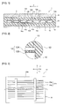
- Fig. 1 is a schematic sectional view of a solar cell module according to one embodiment of the present invention.
- the solar cell module 1 includes a plurality of solar cells 10 arranged along an arrangement direction x.
- the solar cells 10 are electrically connected to one another using wiring members 11.
- the wiring member 11 electrically connects between the adjoining solar cells 10, so that the solar cells 10 are electrically connected to one another in series or in parallel.
- the solar cell 10 and the wiring member 11 are bonded together using a conductive resin adhesive 12.
- the resin adhesive 12 contains a resin 12A and conductive particles 12B dispersed in the resin 12A (see Fig. 2 ). Moreover, it is preferred that the resin adhesive 12 has anisotropic conductivity.
- Examples of a material for the resin 12A in the resin adhesive 12 may include an epoxy resin, an acrylic resin, a polyimide resin, a phenolic resin, a urethane resin, a silicone resin, a mixture or a copolymer of these resins, and the like.
- a particle made of a metal such as nickel, copper, silver, aluminum, tin or gold, or an alloy containing one or more kinds of these metals can be used as the conductive particle 12B contained in the resin adhesive 12.
- the conductive particle 12B may be an insulating particle subjected to conductive coating such as metal coating or alloy coating.
- the insulating particle may include an inorganic oxide particle, a resin particle and the like.
- the inorganic oxide particle may include a particle made of an inorganic oxide such as alumina, silica, titanium oxide or glass.
- the resin particle may include a particle made of an epoxy resin, an acrylic resin, a polyimide resin, a phenolic resin, a urethane resin, a silicone resin, a mixture or a copolymer of these resins, or the like.
- the resin adhesive 12 may contain a different component such as a curing agent.
- the shape of the conductive particle 12B is not particularly limited.
- the conductive particle 12B can take various shapes such as a spherical shape and an ellipsoidal shape.
- First and second protection members 14 and 15 are disposed on a light receiving surface side and a rear surface side of the plurality of solar cells 10.
- a sealant 13 is filled between the first protection member 14 and the second protection member 15. The sealant 13 allows sealing of the plurality of solar cells 10.
- the sealant 13 can be made of an ethylene vinyl acetate copolymer (EVA) or a translucent resin such as polyvinyl butyral (PVB).
- EVA ethylene vinyl acetate copolymer
- PVB polyvinyl butyral
- the first and second protection members 14 and 15 can be formed from glass, resin or the like. Moreover, for example, at least one of the first and second protection members 14 and 15 may be configured with a resin film including a metal foil such as an aluminum foil.
- the first protection member 14 is disposed on the rear surface side of the solar cell 10, and is configured with a resin film including a metal foil such as an aluminum foil.
- the second protection member 15 is disposed on the light receiving surface side of the solar cell 10, and is made of glass or resin.
- Fig. 3 is a schematic plan view seen from the light receiving surface side of the solar cell.
- Fig. 4 is a schematic plan view seen from the rear surface side of the solar cell.
- the solar cell 10 to be described herein is merely one example.
- the type and structure of the solar cell are not intended to be limited.
- the solar cell 10 may be a HIT (registered trademark) solar cell having a HIT structure or may be a solar cell having a different structure.
- the solar cell 10 has one main surface serving as a light receiving surface, and the other main surface serving as a rear surface.
- both the main surfaces of the solar cell may be a light receiving surface.
- each of the first and second protection members 14 and 15 has a translucent property.
- the solar cell 10 includes a photoelectric conversion body 20.
- the photoelectric conversion body 20 receives light, thereby generating carriers (electrons and positive holes).
- the photoelectric conversion body 20 is made of a semiconductor material having a semiconductor junction such as a pn junction or a pin junction.
- the semiconductor material may include a crystalline silicon semiconductor such as single-crystalline silicon or polycrystalline silicon, an amorphous silicon semiconductor, a compound semiconductor such as GaAs, and the like.
- the photoelectric conversion body 20 has a light receiving surface 20a illustrated in Fig. 3 and a rear surface 20b illustrated in Fig. 4 .
- a collector electrode 21a is formed on the light receiving surface 20a
- a collector electrode 21b is formed on the rear surface 20b.
- the collector electrode 21a includes a plurality of finger electrodes 22a and a bus bar 23a
- the collector electrode 21b includes a plurality of finger electrodes 22b and a bus bar 23b.
- the pluralities of finger electrodes 22a and 22b mutually extend in parallel in a direction y perpendicular to the arrangement direction x, respectively.
- the pluralities of finger electrodes 22a and 22b are arranged at predetermined intervals along the arrangement direction x.
- the bus bars 23a and 23b are formed to extend in the arrangement direction x.
- the bus bar 23a connects between the finger electrodes 22a
- the bus bar 23b connects between the finger electrodes 22b.
- carriers generated by the photoelectric conversion body 20 are acquired by the pluralities of finger electrodes 22a and 22b and collected by the bus bars 23a and 23b.
- the collector electrodes 21a and 21b can be formed from a thermosetting conductive paste containing an epoxy resin serving as a binder and a conductive particle serving as a filler.
- the collector electrodes 21a and 21b can be formed by applying the conductive paste in a desired pattern and thermally curing the conductive paste.
- irregularities due to meshes of a screen printing plate are formed on surfaces of the collector electrodes 21a and 21b.
- the collector electrodes 21a and 21b each have a surface roughness falling within a range of 1 ⁇ m to 8 ⁇ m measured by a measuring method using a profilometer based on JIS B0633.
- the collector electrodes 21a and 21b can be formed from a sintering type paste made of a conductive powder containing silver, aluminum or the like, a glass frit, an organic vehicle and the like.
- the collector electrodes 21a and 21b can be configured with a metal film made of silver, aluminum or the like, or an alloy film containing one or more kinds of these metals.
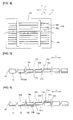
- Fig. 5 is a schematic side view for illustrating a first connecting step. As illustrated in Fig. 5 , first, the adjoining solar cells 10 are electrically connected to each other using the wiring member 11, so that the respective solar cells 10 are electrically connected to one another in series or in parallel using the wiring members 11 (first connecting step).
- the connection between the solar cell 10 and the wiring members 11 is established using the conductive resin adhesive 12.
- a resin adhesive having anisotropic conductivity is used as the resin adhesive 12.
- the resin adhesive 12 used in the first connecting step is referred to as "a resin adhesive 12a".
- a paste-like resin adhesive 12a is applied onto the surface of at least one of the bus bar 23a illustrated in Fig. 3 and the wiring member 11, and is also applied onto the surface of at least one of the bus bar 23b illustrated in Fig. 4 and the wiring member 11.
- a film-like resin adhesive 12a is disposed between the bus bar 23a and the wiring member 11, and is also disposed between the bus bar 23b and the wiring member 11.
- the wiring members 11 are pressed against the bus bars 23a and 23b, respectively, and the resin adhesive 12a is cured in this state.
- the connection between the solar cell 10 and the wiring members 11 is established.
- the wiring member 11 is connected to the whole of the bus bar 23a in the arrangement direction x, and the wiring member 11 is connected to the whole of the bus bar 23b in the arrangement direction x.
- the inspecting step is a step of inspecting the presence or absence of damage as to each of the solar cells 10 connected in the first connecting step.
- This inspecting method is not particularly limited and, for example, may be performed by visual inspection.
- the solar cell 10a determined as being damaged in the inspecting step is exchanged (exchanging step).
- the exchanging step includes a cutting step and a second connecting step.
- the cutting step is a step of cutting a wiring member 11a connecting between the solar cell 10a determined as being damaged and the solar cell 10b adjoining to the solar cell 10a and a wiring member 11b connecting between the solar cell 10a and the solar cell 10c adjoining to the solar cell 10a.
- the wiring members 11a and 11b are cut along cutting lines C1 and C2 illustrated in Fig. 5 , respectively. As illustrated in Fig. 6 , therefore, the wiring member 11a is partially left on the surface of the solar cell 10b, and the wiring member 11b is partially left on the surface of the solar cell 10c.
- the conductive member 16a made of a metal foil which is of the same type as that of the wiring member 11 is bonded to the surface of the solar cell 10b
- the conductive member 16b made of a metal foil which is of the same type as that of the wiring member 11 is bonded to the surface of the solar cell 10c. More specifically, the conductive member 16a is connected to the surface of the bus bar 23b formed on the rear surface 20b of the solar cell 10b (see Fig. 4 ).
- the conductive member 16b is connected to the whole of the surface, in the arrangement direction x, of the bus bar 23a formed on the light receiving surface 20a of the solar cell 10c (see Fig. 3 ).
- a cutting method of the wiring members 11a and 11b is not particularly limited.
- the wiring members 11a and 11b can be cut by a cutting tool such as a cutter.
- the second connecting step is carried out.
- the solar cell 10a determined as being damaged is removed.
- a new solar cell 10d which is not used in the first connecting step is connected to the solar cells 10b and 10c using new wiring members 11c and 11d.
- the solar cell 10d used herein corresponds to a first solar cell.
- the solar cell 10b and the solar cell 10d are connected to each other in such a manner that one side portion of the wiring member 11c and the conductive member 16a provided on the side of the rear surface 20b of the solar cell 10b are bonded together using a resin adhesive 12b having anisotropic conductivity and the other side portion of the wiring member 11c and the bus bar 23a formed on the light receiving surface 20a of the solar cell 10d are bonded together using a resin adhesive 12c having anisotropic conductivity.
- the solar cell 10d and the solar cell 10c are connected to each other in such a manner that one side portion of the wiring member 11d and the bus bar 23b formed on the rear surface 20b of the solar cell 10d are bonded together using a resin adhesive 12d having anisotropic conductivity and the other side portion of the wiring member 11d and the conductive member 16b provided on the side of the light receiving surface 20a of the solar cell 10c are bonded together using a resin adhesive 12e having anisotropic conductivity.
- the wiring member 11 is bonded to substantially the whole of the bus bar 23a in the arrangement direction x, and the wiring member 11 is bonded to substantially the whole of the bus bar 23b in the arrangement direction x. Therefore, the conductive member 16a is bonded to substantially the whole of the solar cell 10b in the arrangement direction x, and the conductive member 16b is bonded to substantially the whole of the solar cell 10c in the arrangement direction x. Also in the second connecting step, the wiring member 11c is bonded to substantially the whole of the bus bar 23a of the solar cell 10d in the arrangement direction x, and the wiring member 11d is bonded to substantially the whole of the bus bar 23b of the solar cell 10d in the arrangement direction x. In the present embodiment, however, the wiring member 11c is connected to only a part of the conductive member 16a in the arrangement direction x, and the wiring member 11d is connected to only a part of the conductive member 16b in the arrangement direction x.
- a module forming step is carried out.
- a resin sheet such as an EVA sheet is placed on the second protection member 15.
- the plurality of solar cells 10 electrically connected to one another using the wiring members 11 is disposed on the resin sheet.
- a resin sheet such as an EVA sheet is placed thereon and, further, the first protection member 14 is placed thereon.
- these components are subjected to thermocompression bonding so as to be temporarily thermocompressively bonded together, and then are heated again, so that the resin sheets are cured.
- the solar cell module 1 may be surrounded with a frame made of metal. Moreover, a terminal box may be attached to the surface of the first protection member 14 in order to take a solar cell output out.
- the resin adhesive 12c used for bonding the solar cell 10d and the wiring member 11c together and the resin adhesive 12d used for bonding the solar cell 10d and the wiring member 11d together have the same composition as that of the resin adhesive 12a used in the first bonding step.
- the resin adhesive 12b for bonding the wiring member 11c and the conductive member 16a corresponding to the left wiring member 11a together and the resin adhesive 12e for bonding the wiring member 11d and the conductive member 16b corresponding to the left wiring member 11b together have different composition from that of the resin adhesive 12a used in the first bonding step and the resin adhesives 12c and 12d.
- a volume content of the conductive particles 12B in the resin adhesives 12b and 12e (see Fig. 2 ) (a volume of the conductive particles 12B per unit volume of each of the resin adhesives 12b and 12e) is larger than a volume content of the conductive particles 12B in the resin adhesives 12a, 12c and 12d.
- the volume content of the conductive particles 12B in the resin adhesives 12b and 12e is not less than 25% by volume.
- the volume content of the conductive particles 12B in the resin adhesives 12a, 12c and 12d is not more than 25% by volume. In the case where the volume content of the conductive particles 12B in the resin adhesives 12b and 12e is 25% by volume, the volume content of the conductive particles 12B in the resin adhesives 12a, 12c and 12d is less than 25% by volume.
- An upper limit value of the volume content of the conductive particles 12B in the resin adhesives 12b and 12e is not particularly limited, but is preferably 58% by volume, more preferably 55% by volume.
- a lower limit value of the volume content of the conductive particles 12B in the resin adhesives 12a, 12c and 12d is not particularly limited, but is preferably 1 ⁇ 10 -4 % by volume, more preferably 5 ⁇ 10 -3 % by volume.
- an average particle diameter of the conductive particles 12B in the resin adhesives 12b and 12e is less than an average particle diameter of the conductive particles 12B in the resin adhesives 12a, 12c and 12d.
- the average particle diameter of the conductive particles 12B in the resin adhesives 12b and 12e is not more than 5 ⁇ m.
- the average particle diameter of the conductive particles 12B in the resin adhesives 12a, 12c and 12d is not less than 5 ⁇ m. In the case where the average particle diameter of the conductive particles 12B in the resin adhesives 12b and 12e is 5 ⁇ m, the average particle diameter of the conductive particles 12B in the resin adhesives 12a, 12c and 12d is less than 5 ⁇ m.
- a lower limit value of the average particle diameter of the conductive particles 12B in the resin adhesives 12b and 12e is not particularly limited, but is preferably 0.1 ⁇ m, more preferably 1 ⁇ m.
- An upper limit value of the average particle diameter of the conductive particles 12B in the resin adhesives 12a, 12c and 12d is not particularly limited, but is preferably 15 ⁇ m, more preferably 10 ⁇ m.
- the volume content of the conductive particles 12B in the resin adhesive 12b for bonding the wiring member 11c and the conductive member 16a together and the resin adhesive 12e for bonding the wiring member 11d and the conductive member 16b together is larger than the volume content of the conductive particles 12B in the resin adhesive 12a for bonding each of the bus bars 23a and 23b and the wiring member 11a together. Therefore, the solar cell module 1 according to the present embodiment is allowed to achieve high output and high heat resistance.
- the volume content of the conductive particles 12B in the resin adhesives 12b and 12e is not less than 25% by volume.
- the volume content of the conductive particles 12B in the resin adhesive 12a is not more than 25% by volume. Accordingly, it is possible to achieve both of high output and high heat resistance.
- the average particle diameter of the conductive particles 12B in the resin adhesives 12b and 12e is less than the average particle diameter of the conductive particles 12B in the resin adhesive 12a. Specifically, the average particle diameter of the conductive particles 12B in the resin adhesives 12b and 12e is not more than 5 ⁇ m. The average particle diameter of the conductive particles 12B in the resin adhesive 12a is not less than 5 ⁇ m. Accordingly, it is possible to achieve both of higher output and higher heat resistance.
- the present invention is not limited to this configuration.
- the conductive members 16 may be bonded to the surfaces of all the solar cells 10.
- the solar cell module 1 according to the foregoing embodiment was prepared with the HIT type solar cell 10 in accordance with the method described in the foregoing embodiment.
- the solar cell module 1 was prepared such that none of the solar cells 10 was damaged in the first connecting step and the solar cell 10a at a specific position out of the plurality of solar cells 10 was exchanged with the new solar cell 10d in the exchanging step.
- a copper foil having both surfaces on which a solder layer made of Sn-Ag-Cu and having a maximum thickness of 40 ⁇ m is formed (a thickness: 150 ⁇ m, a width: 1 mm) was used as the wiring member 11.
- a paste-like adhesive in which conductive particles 12B as Ni particles are dispersed in an epoxy-based resin 12A was used as the conductive resin adhesive 12.
- the resin adhesive 12 was applied onto the bus bars 23a and 23b through the use of a dispenser so as to have a thickness of 20 ⁇ m, a width of 1 mm and a length of 98 mm, and the wiring member 11 was disposed thereon. Thereafter, a metal tool heated to 200°C was pressed with a force of 200 N for 30 seconds, so that the solar cell 10 and the wiring member 11 were bonded together.
- the connection between each of the wiring members 11c and 11d and the solar cell 10d was also established in a similar manner.
- connection between the conductive member 16a and the wiring member 11c and the connection between the conductive member 16b and the wiring member 11d were established as follows. That is, the paste-like resin adhesive 12b was applied onto the conductive member 16a and the paste-like resin adhesive 12e was applied onto the conductive member 16b through the use of the dispenser such that the resin adhesives 12b and 12e have a thickness of 30 ⁇ m, a width of 1 mm and a length of 10 mm. Then, the wiring member 11c was disposed on the resin adhesive 12b and the wiring member 11d was disposed on the resin adhesive 12e.
- the metal tool heated to 200°C was pressed with a force of 1 N for 30 seconds, so that the conductive member 16a and the wiring member 11c were bonded together and the conductive member 16b and the wiring member 11d were bonded together.
- a resin component of each of the resin adhesives 12b and 12e at this time is the same as that of the resin adhesive 12 applied onto the bus bars 23a and 23b.
- the prepared solar cell module 1 was evaluated in accordance with the following method.
- the exchanging step was carried out after measuring output from a unit including the plurality of solar cells 10 before carrying out the cutting step (output before exchange). Thereafter, output from the prepared solar cell module 1 (output after exchange) was measured, and an output ratio ((output after exchange)/(output before exchange)) was calculated.
- the measurement of the output was performed under pseudo sunlight from a solar simulator.
- Evaluation of heat resistance was made in accordance with an evaluation method based on JIS C8992. Specifically, a cycle of heating the prepared solar cell module 1 from -40°C to 90°C over 90 minutes, holding the prepared solar cell module 1 at 90°C for 20 minutes, cooling the prepared solar cell module 1 from 90°C to -40°C over 90 minutes and holding the prepared solar cell module 1 at -40°C for 30 minutes was performed 400 times. After performing the cycle 400 times, output from the solar cell module 1 was measured, and a ratio of output after conducting the heat resistance test to output before conducting the heat resistance test (corresponding to the output after exchange) ((output after conducting heat resistance test) / (output before conducting heat resistance test)) was calculated.
- Data shown in Table 1 below are data obtained by preparing and evaluating the solar cell module 1 while variously changing the volume content of the conductive particles 12B in the resin adhesive 12b used for connecting the conductive member 16a and the wiring member 11c in the second connecting step and the resin adhesive 12e used for connecting the conductive member 16b and the wiring member 11d in the second connecting step.
- an adhesive containing conductive particles 12B having an average particle diameter of 7 ⁇ m and a volume content of 1 ⁇ 10 -2 % was used as the resin adhesive 12a used in the first connecting step.
- the average particle diameter of the conductive particles 12B in the resin adhesives 12b and 12e was set to 2 ⁇ m.
- Table 1 Volume content of conductive particles 12B in conductive adhesives 12b and 12e (% by volume) (Output after exchange)/ (output before exchange) (Output after conducting heat resistance test)/ (output before conducting heat resistance test) 5 ⁇ 10 -3 98.2% 99.5% 10 99.2% 99.6% 20 99.4% 99.5% 25 99.8% 99.4% 30 100% 99.5% 40 100% 99.6% 55 99.8% 99.2%
- Data shown in Table 2 below are data obtained by preparing and evaluating the solar cell module 1 while variously changing the volume content of the conductive particles 12B in the resin adhesive 12a used in the first connecting step.
- an adhesive containing conductive particles 12B having an average particle diameter of 2 ⁇ m and a volume content of 50% was used as the resin adhesives 12b and 12e.
- the average particle diameter of the conductive particles 12B in the resin adhesive 12a used in the first connecting step was set to 7 ⁇ m.
- Data shown in Table 3 below are data obtained by preparing and evaluating the solar cell module 1 while variously changing the average particle diameter of the conductive particles 12B in the resin adhesive 12b used for connecting the conductive member 16a and the wiring member 11c in the second connecting step and the resin adhesive 12e used for connecting the conductive member 16b and the wiring member 11d in the second connecting step.
- an adhesive containing conductive particles 12B having an average particle diameter of 7 ⁇ m and a volume content of 1 ⁇ 10 -2 % was used as the resin adhesive 12 used in the first connecting step.
- the volume content of the conductive particles 12B in the resin adhesives 12b and 12e was set to 30% by volume.
- Data shown in Table 4 below are data obtained by preparing and evaluating the solar cell module 1 while variously changing the average particle diameter of the conductive particles 12B in the resin adhesive 12a used in the first connecting step.
- an adhesive containing conductive particles 12B having an average particle diameter of 2 ⁇ m and a volume content of 50% was used as the resin adhesives 12b and 12e.
- the volume content of the conductive particles 12B in the resin adhesive 12a used in the first connecting step was set to 1 ⁇ 10 -2 % by volume.
- the (output after exchange) / (output before exchange) tended to decrease as the volume content of the conductive particles 12B was set to be small.
- the heat resistance did not change largely even when the volume content of the conductive particles 12B in the resin adhesives 12b and 12e was changed.
- a solar cell module 1 was prepared and evaluated in similar manners to those in the foregoing experimental example except that the solar cell 10 and the wiring member 11 were bonded together by using solder made of an SnAgCu alloy in place of the resin adhesive 12, pressing the wiring member 11 with a force of 1 N and heating the solder to 250°C.
- the (output after exchange) / (output before exchange) was 99.5%
- the output ratio ((output after conducting heat resistance test)/(output before conducting heat resistance test)) was 98.3%. It is apparent from this result that it is possible to realize high output and high heat resistance by using the resin adhesive 12 for bonding the solar cell 10 and the wiring member 11 together as in the present embodiment.
- a curing temperature of the resin adhesive 12b for bonding the wiring member 11c and the conductive member 16a corresponding to the left wiring member 11a together and the resin adhesive 12e for bonding the wiring member 11d and the conductive member 16b corresponding to the left wiring member 11b together is lower than a curing temperature of the resin adhesive 12a used in the first bonding step and the resin adhesives 12c and 12d.
- a curing temperature of a resin adhesive can be optionally determined how blended a curing agent is.
- Table 5 shows results obtained in the case of using a conductive adhesive manufactured by Diemat, Inc. As shown in this table, it is preferred that conductive pastes which are different in curing temperature from one another may be selectively used by appropriately adjusting the type and amount of a curing agent to be blended in a resin adhesive.
Landscapes
- Photovoltaic Devices (AREA)
Abstract
Description
- This invention relates to a solar cell module and a manufacturing method of the same. Particularly, this invention relates to a solar cell module including a plurality of solar cells electrically connected to one another using wiring members, and a manufacturing method of the same.
- Recently, great attention has been given to solar cell modules as an energy source with small load on an environment.
- Typically, a solar cell module includes a plurality of solar cells. The solar cells are electrically connected to one another in series or in parallel using wiring members.
- Conventionally, solder has been widely used for bonding a solar cell and a wiring member together. In order to bond the solar cell and the wiring member together using the solder, however, there is a necessity to melt the solder. Consequently, there is a possibility that in a bonding step, the solar cell is heated to high temperature, whereby the solar cell is damaged or becomes deformed.
- In view of this, for example,
JP 2009-295940 A -
- Patent Literature 1:
JP 2009-295940 A - Incidentally, in a solar cell module manufacturing process, some solar cells are occasionally damaged. In the case where a solar cell is damaged, there is a necessity to exchange the damaged solar cell with a new solar cell.
- In order to perform the exchange of the solar cell, typically, wiring members connected to the damaged solar cell are cut, and then the damaged solar cell is removed. Next, a new solar cell is mounted, and the new solar cell and the wiring members left on the solar cells each adjoining to the new solar cell are bonded together using wiring members.
- In the case where the solar cell and the wiring member are bonded together using a conductive resin adhesive, typically, it is considered that a conductive resin adhesive which is of the same type as the conductive resin adhesive used for bonding the solar cell and the wiring member together is preferably used for bonding the wiring members together.
- As a result of the study eagerly conducted by the inventor of the present invention, however, it has been newly found that a solar cell module, wherein the conductive resin adhesive which is of the same type as the conductive resin adhesive used for bonding the solar cell and the wiring member together is used for bonding the wiring members together, is inferior in output or heat resistance to a solar cell module wherein no solar cell is exchanged.
- The present invention has been devised in view of the circumstances described above, and an object thereof is to provide a solar cell module including a plurality of solar cells connected to one another using wiring members, and achieving high output and high heat resistance.
- A solar cell module according to an aspect of the present invention includes a plurality of solar cells, a wiring member and a resin adhesive. The wiring member electrically connects between the solar cells. The resin adhesive bonds the wiring member and the solar cell together. The resin adhesive contains a resin and conductive particles dispersed in the resin. The plurality of solar cells includes a first solar cell and a second solar cell adjoining to the first solar cell. The first solar cell has a surface to which the conductive member made of a metal foil is bonded. The first solar cell and the second solar cell are electrically connected to each other in such a manner that the conductive member and one side portion of the wiring member are bonded together using the resin adhesive and the other side portion of the wiring member and the second solar cell are bonded together using the resin adhesive. A volume content of the conductive particles in the resin adhesive bonding the conductive member and the wiring member together is larger than a volume content of the conductive particles in the resin adhesive bonding the wiring member and the solar cell together.
- In the solar cell module according to the aspect, it is preferred that the volume content of the conductive particles in the resin adhesive for bonding the conductive member and the wiring member together is not less than 25% by volume.
- In the solar cell module according to the aspect, it is preferred that the volume content of the conductive particles in the resin adhesive for bonding the wiring member and the solar cell together is not more than 25% by volume.
- In the solar cell module according to the aspect, it is preferred that an average particle diameter of the conductive particles in the resin adhesive for bonding the conductive member and the wiring member together is less than an average particle diameter of the conductive particles in the resin adhesive for bonding the wiring member and the solar cell together. In this case, it is preferred that the average particle diameter of the conductive particles in the resin adhesive for bonding the conductive member and the wiring member together is not more than 5 µm. It is preferred that the average particle diameter of the conductive particles in the resin adhesive for bonding the wiring member and the solar cell together is not less than 5 µm.
- In the present invention, the average particle diameter of the conductive particles refers to a value obtained by measuring laser diffraction and scattering through the use of a laser diffraction and scattering particle-size distribution analyzer (LA-700) manufactured by Horiba, Ltd.
- In the solar cell module according to the aspect, the wiring member may be bonded to the whole of the solar cell in an arrangement direction of the plurality of solar cells, and the conductive member may be bonded to the whole of the first solar cell in the arrangement direction while the wiring member may be bonded to a part of the conductive member in the arrangement direction.
- A manufacturing method of a solar cell module according to an aspect of the present invention includes a first connecting step, an inspecting step and an exchanging step. The first connecting step is a step of electrically connecting a plurality of solar cells using a wiring member by bonding the solar cell and the wiring member together using a resin adhesive containing a resin and conductive particles dispersed in the resin. The inspecting step is a step of inspecting the presence or absence of damage as to each of the connected solar cells. The exchanging step is a step of exchanging a solar cell determined as being damaged in the inspecting step. The exchanging step includes a cutting step and a second connecting step. The cutting step is a step of cutting the wiring member connecting between the solar cell determined as being damaged and the solar cell adjoining to the damaged solar cell. The second connecting step is a step of bonding a new solar cell and one side portion of a new wiring member together using the resin adhesive and bonding the other side portion of the new wiring member and the left wiring member bonded to the solar cell, which has adjoined to the solar cell determined as being damaged, together using the resin adhesive to electrically connect between the new solar cell and the solar cell which has adjoined to the solar cell determined as being damaged. A volume content of the conductive particles in the resin adhesive bonding the other side portion of the wiring member and the left wiring member together is larger than a volume content of the conductive particles in the resin adhesive used in the first connecting step.
- In the present invention, the "new solar cell" indicates a solar cell which is not used in the first connecting step, and does not necessarily indicate a brand-new solar cell. Likewise, the "new wiring member" indicates a wiring member which is not used in the first connecting step, and does not necessarily indicate a brand-new wiring member.
- In the manufacturing method of the solar cell module according to the aspect, it is preferred that the volume content of the conductive particles in the resin adhesive for bonding the other side portion of the wiring member and the left wiring member together is not less than 25% by volume.
- In the manufacturing method of the solar cell module according to the aspect, it is preferred that the volume content of the conductive particles in the resin adhesive used in the first connecting step is not more than 25% by volume.
- In the manufacturing method of the solar cell module according to the aspect, it is preferred that an average particle diameter of the conductive particles in the resin adhesive for bonding the other side portion of the wiring member and the left wiring member together is less than an average particle diameter of the conductive particles in the resin adhesive used in the first connecting step.
- In the manufacturing method of the solar cell module according to the aspect, it is preferred that the average particle diameter of the conductive particles in the resin adhesive for bonding the other side portion of the wiring member and the left wiring member together is not more than 5 µm.
- In the manufacturing method of the solar cell module according to the aspect, it is preferred that the average particle diameter of the conductive particles in the resin adhesive used in the first connecting step is not less than 5 µm.
- In the manufacturing method of the solar cell module according to the aspect, in the first connecting step, the wiring member may be bonded to the whole of the solar cell in an arrangement direction of the plurality of solar cells, and in the second connecting step, the one side portion of the new wiring member may be bonded to the whole of the new solar cell in the arrangement direction of the plurality of solar cells while the other side portion of the new wiring member may be bonded to a part, in the arrangement direction, of the left wiring member bonded to the solar cell which has adjoined to the solar cell determined as being damaged.
- According to the present invention, it is possible to provide a solar cell module including a plurality of solar cells connected to one another using wiring members, and achieving high output and high heat resistance.
-
- [
Fig. 1 ]
Fig. 1 is a schematic sectional view of a solar cell module according to one embodiment of the present invention. - [
Fig. 2 ]
Fig. 2 is a schematic sectional view of a portion II inFig. 1 . - [
Fig. 3 ]
Fig. 3 is a schematic plan view seen from a light receiving surface side of a solar cell. - [
Fig. 4 ]
Fig. 4 is a schematic plan view seen from a rear surface side of the solar cell. - [
Fig. 5 ]
Fig. 5 is a schematic side view for illustrating a first connecting step. - [
Fig. 6 ]
Fig. 6 is a schematic side view for illustrating a second connecting step. - A preferred embodiment of the present invention will be described below with a solar cell module 1 in
Fig. 1 taken as an example. However, the solar cell module 1 is merely illustrative. The present invention is not intended to be limited to the solar cell module 1. - Throughout the respective drawings to be referred in the embodiment and the like, moreover, members having substantially identical functions are denoted with identical reference signs. Moreover, the drawings to be referred in the embodiment and the like are schematically made, and the dimensional ratio and the like of a physical object depicted in the drawings occasionally differ from the dimensional ratio and the like of an actual physical object. The respective drawings occasionally differ from one another with regard to the dimensional ratio and the like of a physical object. The dimensional ratio and the like of a specific physical object should be determined in consideration of the following description.
-
Fig. 1 is a schematic sectional view of a solar cell module according to one embodiment of the present invention. - As illustrated in
Fig. 1 , the solar cell module 1 includes a plurality ofsolar cells 10 arranged along an arrangement direction x. Thesolar cells 10 are electrically connected to one another usingwiring members 11. Specifically, thewiring member 11 electrically connects between the adjoiningsolar cells 10, so that thesolar cells 10 are electrically connected to one another in series or in parallel. - In the present embodiment, the
solar cell 10 and thewiring member 11 are bonded together using aconductive resin adhesive 12. Theresin adhesive 12 contains aresin 12A andconductive particles 12B dispersed in theresin 12A (seeFig. 2 ). Moreover, it is preferred that theresin adhesive 12 has anisotropic conductivity. - Examples of a material for the
resin 12A in theresin adhesive 12 may include an epoxy resin, an acrylic resin, a polyimide resin, a phenolic resin, a urethane resin, a silicone resin, a mixture or a copolymer of these resins, and the like. - For example, a particle made of a metal such as nickel, copper, silver, aluminum, tin or gold, or an alloy containing one or more kinds of these metals can be used as the
conductive particle 12B contained in theresin adhesive 12. Moreover, theconductive particle 12B may be an insulating particle subjected to conductive coating such as metal coating or alloy coating. Examples of the insulating particle may include an inorganic oxide particle, a resin particle and the like. Examples of the inorganic oxide particle may include a particle made of an inorganic oxide such as alumina, silica, titanium oxide or glass. Examples of the resin particle may include a particle made of an epoxy resin, an acrylic resin, a polyimide resin, a phenolic resin, a urethane resin, a silicone resin, a mixture or a copolymer of these resins, or the like. - Moreover, the
resin adhesive 12 may contain a different component such as a curing agent. - The shape of the
conductive particle 12B is not particularly limited. Theconductive particle 12B can take various shapes such as a spherical shape and an ellipsoidal shape. - First and
second protection members 14 and 15 are disposed on a light receiving surface side and a rear surface side of the plurality ofsolar cells 10. Asealant 13 is filled between the first protection member 14 and thesecond protection member 15. Thesealant 13 allows sealing of the plurality ofsolar cells 10. - Materials for the
sealant 13 as well as the first andsecond protection members 14 and 15 are not particularly limited. For example, thesealant 13 can be made of an ethylene vinyl acetate copolymer (EVA) or a translucent resin such as polyvinyl butyral (PVB). - For example, the first and
second protection members 14 and 15 can be formed from glass, resin or the like. Moreover, for example, at least one of the first andsecond protection members 14 and 15 may be configured with a resin film including a metal foil such as an aluminum foil. In the present embodiment, the first protection member 14 is disposed on the rear surface side of thesolar cell 10, and is configured with a resin film including a metal foil such as an aluminum foil. Thesecond protection member 15 is disposed on the light receiving surface side of thesolar cell 10, and is made of glass or resin. -
Fig. 3 is a schematic plan view seen from the light receiving surface side of the solar cell.Fig. 4 is a schematic plan view seen from the rear surface side of the solar cell. - It is noted that the
solar cell 10 to be described herein is merely one example. In the present invention, the type and structure of the solar cell are not intended to be limited. For example, thesolar cell 10 may be a HIT (registered trademark) solar cell having a HIT structure or may be a solar cell having a different structure. - In the present embodiment, moreover, the
solar cell 10 has one main surface serving as a light receiving surface, and the other main surface serving as a rear surface. In the present invention, however, both the main surfaces of the solar cell may be a light receiving surface. In this case, it is preferred that each of the first andsecond protection members 14 and 15 has a translucent property. - As illustrated in
Figs. 3 and4 , thesolar cell 10 includes aphotoelectric conversion body 20. Thephotoelectric conversion body 20 receives light, thereby generating carriers (electrons and positive holes). - The
photoelectric conversion body 20 is made of a semiconductor material having a semiconductor junction such as a pn junction or a pin junction. Examples of the semiconductor material may include a crystalline silicon semiconductor such as single-crystalline silicon or polycrystalline silicon, an amorphous silicon semiconductor, a compound semiconductor such as GaAs, and the like. - The
photoelectric conversion body 20 has alight receiving surface 20a illustrated inFig. 3 and arear surface 20b illustrated inFig. 4 . Acollector electrode 21a is formed on thelight receiving surface 20a, and acollector electrode 21b is formed on therear surface 20b. Thecollector electrode 21a includes a plurality offinger electrodes 22a and abus bar 23a, and thecollector electrode 21b includes a plurality offinger electrodes 22b and abus bar 23b. The pluralities offinger electrodes finger electrodes bus bar 23a connects between thefinger electrodes 22a, and thebus bar 23b connects between thefinger electrodes 22b. - In the
solar cell 10, carriers generated by thephotoelectric conversion body 20 are acquired by the pluralities offinger electrodes - For example, the
collector electrodes collector electrodes collector electrodes collector electrodes collector electrodes - Moreover, for example, the
collector electrodes collector electrodes - Next, a manufacturing method of the solar cell module 1 will be described with main reference to
Figs. 1 ,5 and 6 . -
Fig. 5 is a schematic side view for illustrating a first connecting step. As illustrated inFig. 5 , first, the adjoiningsolar cells 10 are electrically connected to each other using thewiring member 11, so that the respectivesolar cells 10 are electrically connected to one another in series or in parallel using the wiring members 11 (first connecting step). - In the first connecting step, the connection between the
solar cell 10 and thewiring members 11 is established using theconductive resin adhesive 12. A resin adhesive having anisotropic conductivity is used as theresin adhesive 12. (Hereinafter, theresin adhesive 12 used in the first connecting step is referred to as "a resin adhesive 12a".) Specifically, a paste-like resin adhesive 12a is applied onto the surface of at least one of thebus bar 23a illustrated inFig. 3 and thewiring member 11, and is also applied onto the surface of at least one of thebus bar 23b illustrated inFig. 4 and thewiring member 11. Alternatively, a film-like resin adhesive 12a is disposed between thebus bar 23a and thewiring member 11, and is also disposed between thebus bar 23b and thewiring member 11. Thereafter, thewiring members 11 are pressed against the bus bars 23a and 23b, respectively, and theresin adhesive 12a is cured in this state. Thus, the connection between thesolar cell 10 and thewiring members 11 is established. In the present embodiment, thewiring member 11 is connected to the whole of thebus bar 23a in the arrangement direction x, and thewiring member 11 is connected to the whole of thebus bar 23b in the arrangement direction x. - Next, an inspecting step is carried out. The inspecting step is a step of inspecting the presence or absence of damage as to each of the
solar cells 10 connected in the first connecting step. This inspecting method is not particularly limited and, for example, may be performed by visual inspection. - In the present embodiment, it is assumed in the inspecting step that only a
solar cell 10a is determined as being damaged out of the plurality ofsolar cells 10 illustrated inFig. 5 . That is, in the present embodiment,solar cells - Next, the
solar cell 10a determined as being damaged in the inspecting step is exchanged (exchanging step). Specifically, the exchanging step includes a cutting step and a second connecting step. - The cutting step is a step of cutting a
wiring member 11a connecting between thesolar cell 10a determined as being damaged and thesolar cell 10b adjoining to thesolar cell 10a and awiring member 11b connecting between thesolar cell 10a and thesolar cell 10c adjoining to thesolar cell 10a. In the present embodiment, in the cutting step, thewiring members Fig. 5 , respectively. As illustrated inFig. 6 , therefore, thewiring member 11a is partially left on the surface of thesolar cell 10b, and thewiring member 11b is partially left on the surface of thesolar cell 10c. Thus, theconductive member 16a made of a metal foil which is of the same type as that of thewiring member 11 is bonded to the surface of thesolar cell 10b, and theconductive member 16b made of a metal foil which is of the same type as that of thewiring member 11 is bonded to the surface of thesolar cell 10c. More specifically, theconductive member 16a is connected to the surface of thebus bar 23b formed on therear surface 20b of thesolar cell 10b (seeFig. 4 ). Theconductive member 16b is connected to the whole of the surface, in the arrangement direction x, of thebus bar 23a formed on thelight receiving surface 20a of thesolar cell 10c (seeFig. 3 ). - Herein, a cutting method of the
wiring members wiring members - Subsequent to the cutting step, the second connecting step is carried out. First, the
solar cell 10a determined as being damaged is removed. As illustrated inFig. 6 , then, a newsolar cell 10d which is not used in the first connecting step is connected to thesolar cells new wiring members solar cell 10d used herein corresponds to a first solar cell. - Specifically, the
solar cell 10b and thesolar cell 10d are connected to each other in such a manner that one side portion of thewiring member 11c and theconductive member 16a provided on the side of therear surface 20b of thesolar cell 10b are bonded together using a resin adhesive 12b having anisotropic conductivity and the other side portion of thewiring member 11c and thebus bar 23a formed on thelight receiving surface 20a of thesolar cell 10d are bonded together using a resin adhesive 12c having anisotropic conductivity. Thesolar cell 10d and thesolar cell 10c are connected to each other in such a manner that one side portion of thewiring member 11d and thebus bar 23b formed on therear surface 20b of thesolar cell 10d are bonded together using aresin adhesive 12d having anisotropic conductivity and the other side portion of thewiring member 11d and theconductive member 16b provided on the side of thelight receiving surface 20a of thesolar cell 10c are bonded together using a resin adhesive 12e having anisotropic conductivity. - In the first connecting step, the
wiring member 11 is bonded to substantially the whole of thebus bar 23a in the arrangement direction x, and thewiring member 11 is bonded to substantially the whole of thebus bar 23b in the arrangement direction x. Therefore, theconductive member 16a is bonded to substantially the whole of thesolar cell 10b in the arrangement direction x, and theconductive member 16b is bonded to substantially the whole of thesolar cell 10c in the arrangement direction x. Also in the second connecting step, thewiring member 11c is bonded to substantially the whole of thebus bar 23a of thesolar cell 10d in the arrangement direction x, and thewiring member 11d is bonded to substantially the whole of thebus bar 23b of thesolar cell 10d in the arrangement direction x. In the present embodiment, however, thewiring member 11c is connected to only a part of theconductive member 16a in the arrangement direction x, and thewiring member 11d is connected to only a part of theconductive member 16b in the arrangement direction x. - After termination of the second connecting step, a module forming step is carried out. In this step, for example, a resin sheet such as an EVA sheet is placed on the
second protection member 15. The plurality ofsolar cells 10 electrically connected to one another using thewiring members 11 is disposed on the resin sheet. A resin sheet such as an EVA sheet is placed thereon and, further, the first protection member 14 is placed thereon. Under an atmosphere of reduced pressure, these components are subjected to thermocompression bonding so as to be temporarily thermocompressively bonded together, and then are heated again, so that the resin sheets are cured. Through the steps described above, the solar cell module 1 can be manufactured. - If necessary, the solar cell module 1 may be surrounded with a frame made of metal. Moreover, a terminal box may be attached to the surface of the first protection member 14 in order to take a solar cell output out.
- In the present embodiment, in the second connecting step, the resin adhesive 12c used for bonding the
solar cell 10d and thewiring member 11c together and theresin adhesive 12d used for bonding thesolar cell 10d and thewiring member 11d together have the same composition as that of theresin adhesive 12a used in the first bonding step. On the other hand, in the second connecting step, the resin adhesive 12b for bonding thewiring member 11c and theconductive member 16a corresponding to theleft wiring member 11a together and the resin adhesive 12e for bonding thewiring member 11d and theconductive member 16b corresponding to theleft wiring member 11b together have different composition from that of theresin adhesive 12a used in the first bonding step and theresin adhesives - Specifically, a volume content of the
conductive particles 12B in theresin adhesives Fig. 2 ) (a volume of theconductive particles 12B per unit volume of each of theresin adhesives conductive particles 12B in theresin adhesives conductive particles 12B in theresin adhesives conductive particles 12B in theresin adhesives conductive particles 12B in theresin adhesives conductive particles 12B in theresin adhesives - An upper limit value of the volume content of the
conductive particles 12B in theresin adhesives conductive particles 12B in theresin adhesives - Further, an average particle diameter of the
conductive particles 12B in theresin adhesives Fig. 2 ) is less than an average particle diameter of theconductive particles 12B in theresin adhesives conductive particles 12B in theresin adhesives conductive particles 12B in theresin adhesives conductive particles 12B in theresin adhesives conductive particles 12B in theresin adhesives - A lower limit value of the average particle diameter of the
conductive particles 12B in theresin adhesives conductive particles 12B in theresin adhesives - As described above, in the present embodiment, the volume content of the
conductive particles 12B in the resin adhesive 12b for bonding thewiring member 11c and theconductive member 16a together and the resin adhesive 12e for bonding thewiring member 11d and theconductive member 16b together is larger than the volume content of theconductive particles 12B in the resin adhesive 12a for bonding each of the bus bars 23a and 23b and thewiring member 11a together. Therefore, the solar cell module 1 according to the present embodiment is allowed to achieve high output and high heat resistance. - Moreover, at the time of bonding the
wiring member 11c and theconductive member 16a together and bonding thewiring member 11d and theconductive member 16b together, even in the case where a pressure to be applied between the wiringmember 11c and theconductive member 16a and between thewiring member 11d and theconductive member 16b is set to be small, it is possible to appropriately bond thewiring member 11c and theconductive member 16a together and to appropriately bond thewiring member 11d and theconductive member 16b together. Accordingly, it is possible to prevent thesolar cell 10 from being damaged in the second bonding step. Accordingly, it is possible to manufacture thesolar cell 10 with high efficiency percentage. - Specifically, in the present embodiment, the volume content of the
conductive particles 12B in theresin adhesives conductive particles 12B in theresin adhesive 12a is not more than 25% by volume. Accordingly, it is possible to achieve both of high output and high heat resistance. - Further, the average particle diameter of the
conductive particles 12B in theresin adhesives conductive particles 12B in theresin adhesive 12a. Specifically, the average particle diameter of theconductive particles 12B in theresin adhesives conductive particles 12B in theresin adhesive 12a is not less than 5 µm. Accordingly, it is possible to achieve both of higher output and higher heat resistance. - In the present embodiment, the description is given of the example that the conductive members 16 are bonded to the surfaces of some of the
solar cell 10. However, the present invention is not limited to this configuration. For example, the conductive members 16 may be bonded to the surfaces of all thesolar cells 10. - The foregoing advantageous effects will be specifically described below on the basis of examples of actually conducted experiments.
- In the present experimental example, the solar cell module 1 according to the foregoing embodiment was prepared with the HIT type
solar cell 10 in accordance with the method described in the foregoing embodiment. In the present experimental example, however, the solar cell module 1 was prepared such that none of thesolar cells 10 was damaged in the first connecting step and thesolar cell 10a at a specific position out of the plurality ofsolar cells 10 was exchanged with the newsolar cell 10d in the exchanging step. - A copper foil having both surfaces on which a solder layer made of Sn-Ag-Cu and having a maximum thickness of 40 µm is formed (a thickness: 150 µm, a width: 1 mm) was used as the
wiring member 11. - A paste-like adhesive in which
conductive particles 12B as Ni particles are dispersed in an epoxy-basedresin 12A was used as theconductive resin adhesive 12. Theresin adhesive 12 was applied onto the bus bars 23a and 23b through the use of a dispenser so as to have a thickness of 20 µm, a width of 1 mm and a length of 98 mm, and thewiring member 11 was disposed thereon. Thereafter, a metal tool heated to 200°C was pressed with a force of 200 N for 30 seconds, so that thesolar cell 10 and thewiring member 11 were bonded together. The connection between each of thewiring members solar cell 10d was also established in a similar manner. - When the metal tool was pressed with the force of 200 N, a pressure of about 2 MPa was applied to the
wiring member 11. - On the other hand, the connection between the
conductive member 16a and thewiring member 11c and the connection between theconductive member 16b and thewiring member 11d were established as follows. That is, the paste-like resin adhesive 12b was applied onto theconductive member 16a and the paste-like resin adhesive 12e was applied onto theconductive member 16b through the use of the dispenser such that theresin adhesives wiring member 11c was disposed on the resin adhesive 12b and thewiring member 11d was disposed on theresin adhesive 12e. Thereafter, the metal tool heated to 200°C was pressed with a force of 1 N for 30 seconds, so that theconductive member 16a and thewiring member 11c were bonded together and theconductive member 16b and thewiring member 11d were bonded together. It is noted that a resin component of each of theresin adhesives resin adhesive 12 applied onto the bus bars 23a and 23b. - When the metal tool was pressed with the force of 1 N, a pressure of almost 0.1 MPa was applied to the
wiring members - Moreover, the prepared solar cell module 1 was evaluated in accordance with the following method.
- The exchanging step was carried out after measuring output from a unit including the plurality of
solar cells 10 before carrying out the cutting step (output before exchange). Thereafter, output from the prepared solar cell module 1 (output after exchange) was measured, and an output ratio ((output after exchange)/(output before exchange)) was calculated. Herein, the measurement of the output was performed under pseudo sunlight from a solar simulator. - Evaluation of heat resistance was made in accordance with an evaluation method based on JIS C8992. Specifically, a cycle of heating the prepared solar cell module 1 from -40°C to 90°C over 90 minutes, holding the prepared solar cell module 1 at 90°C for 20 minutes, cooling the prepared solar cell module 1 from 90°C to -40°C over 90 minutes and holding the prepared solar cell module 1 at -40°C for 30 minutes was performed 400 times. After performing the cycle 400 times, output from the solar cell module 1 was measured, and a ratio of output after conducting the heat resistance test to output before conducting the heat resistance test (corresponding to the output after exchange) ((output after conducting heat resistance test) / (output before conducting heat resistance test)) was calculated.
- Data shown in Table 1 below are data obtained by preparing and evaluating the solar cell module 1 while variously changing the volume content of the
conductive particles 12B in the resin adhesive 12b used for connecting theconductive member 16a and thewiring member 11c in the second connecting step and theresin adhesive 12e used for connecting theconductive member 16b and thewiring member 11d in the second connecting step. Herein, an adhesive containingconductive particles 12B having an average particle diameter of 7 µm and a volume content of 1×10⁻²% was used as theresin adhesive 12a used in the first connecting step. Moreover, the average particle diameter of theconductive particles 12B in theresin adhesives -
Table 1 Volume content of conductive particles 12B inconductive adhesives (Output after exchange)/
(output before exchange)(Output after conducting heat resistance test)/
(output before conducting heat resistance test)5×10⁻³ 98.2% 99.5% 10 99.2% 99.6% 20 99.4% 99.5% 25 99.8% 99.4% 30 100% 99.5% 40 100% 99.6% 55 99.8% 99.2% - Data shown in Table 2 below are data obtained by preparing and evaluating the solar cell module 1 while variously changing the volume content of the
conductive particles 12B in theresin adhesive 12a used in the first connecting step. Herein, an adhesive containingconductive particles 12B having an average particle diameter of 2 µm and a volume content of 50% was used as theresin adhesives conductive particles 12B in theresin adhesive 12a used in the first connecting step was set to 7 µm. -
Table 2 Volume content of conductive particles 12B inconductive adhesive 12a (% by volume)(Output after exchange)/
(output before exchange)(Output after conducting heat resistance test)/
(output before conducting heat resistance test)5×10⁻³ 100% 99.5% 1 100% 99.4% 10 100% 99.5% 20 100% 99.5% 25 100% 99.3% 30 100% 98.2% 35 100% 95.3% - Data shown in Table 3 below are data obtained by preparing and evaluating the solar cell module 1 while variously changing the average particle diameter of the
conductive particles 12B in the resin adhesive 12b used for connecting theconductive member 16a and thewiring member 11c in the second connecting step and theresin adhesive 12e used for connecting theconductive member 16b and thewiring member 11d in the second connecting step. Herein, an adhesive containingconductive particles 12B having an average particle diameter of 7 µm and a volume content of 1×10⁻²% was used as theresin adhesive 12 used in the first connecting step. Moreover, the volume content of theconductive particles 12B in theresin adhesives -
Table 3 Average particle diameter of conductive particles 12B inconductive adhesives (Output after exchange)/
(output before exchange)(Output after conducting heat resistance test)/
(output before conducting heat resistance test)1 100% 99.6% 3 100% 99.5% 5 99.8% 99.6% 7 99.4% 99.5% 10 98.8% 99.5% - Data shown in Table 4 below are data obtained by preparing and evaluating the solar cell module 1 while variously changing the average particle diameter of the
conductive particles 12B in theresin adhesive 12a used in the first connecting step. Herein, an adhesive containingconductive particles 12B having an average particle diameter of 2 µm and a volume content of 50% was used as theresin adhesives conductive particles 12B in theresin adhesive 12a used in the first connecting step was set to 1×10⁻²% by volume. -
Table 4 Average particle diameter of conductive particles 12B inconductive adhesive 12a (µm)(Output after exchange)/
(output before exchange)(Output after conducting heat resistance test)/
(output before conducting heat resistance test)1 98.2% 98.3% 3 99.0% 99.1% 5 99.8% 99.3% 7 100% 99.5% 10 100% 99.5% - It is apparent from the results shown in Table 1 above that the (output after exchange)/(output before exchange) tended to decrease as the volume content of
conductive particles 12B in the resin adhesive 12b used for connecting between theconductive member 16a and thewiring member 11c in the second connecting step and theresin adhesive 12e used for connecting between theconductive member 16b and thewiring member 11d in the second connecting step was set to be small. Specifically, in the case where the volume content of theconductive particles 12B in theresin adhesives conductive particles 12B was changed. On the other hand, in the case where the volume content of theconductive particles 12B in theresin adhesives conductive particles 12B was set to be small. - The heat resistance did not change largely even when the volume content of the
conductive particles 12B in theresin adhesives - It is apparent from the results shown in Table 2 above that the (output after exchange) / (output before exchange) did not change even when the volume content of the
conductive particles 12B in theresin adhesive 12a used in the first connecting step was changed. On the other hand, the heat resistance tended to decrease as the volume content of theconductive particles 12B in the resin adhesive 12a was set to be large. Specifically, in the case where the volume content of theconductive particles 12B in the resin adhesive 12a was not more than 25% by volume, the heat resistance did not change even when the volume content of theconductive particles 12B was changed. However, it is apparent that the volume content of theconductive particles 12B increases and the heat resistance decreases in the case where the volume content of theconductive particles 12B in theresin adhesive 12a is larger than 25% by volume. - It is apparent from the results described above that it is difficult to achieve both of high output and high heat resistance in the case where the
resin adhesives conductive particles 12B. Specifically, it is apparent that it becomes difficult to achieve high output in the case where the volume content of theconductive particles 12B in theresin adhesives conductive particles 12B in theresin adhesive 12a is larger than 25% by volume. - Moreover, it is apparent that it is possible to achieve both of high output and high heat resistance when the volume content of the
conductive particles 12B in theresin adhesives conductive particles 12B in theresin adhesive 12a. Specifically, it is apparent that it is possible to achieve both of high output and high heat resistance when the volume content of theconductive particles 12B in theresin adhesives conductive particles 12B in theresin adhesive 12a is set to be not more than 25% by volume and the volume content of theconductive particles 12B in theresin adhesives conductive particles 12B in theresin adhesive 12a. - Moreover, it is apparent from the results shown in Table 3 that the heat resistance does not change so much even when the average particle diameter of the
conductive particles 12B in theresin adhesives conductive particles 12B in theresin adhesives conductive particles 12B in theresin adhesives conductive particles 12B in theresin adhesives conductive particles 12B in theresin adhesives conductive particles 12B in theresin adhesives - It is apparent from the results shown in Table 4 that both the (output after exchange)/(output before exchange) and the heat resistance decrease as the average particle diameter of the
conductive particles 12B in theresin adhesive 12a is set to be small. Specifically, in the case where the average particle diameter of theconductive particles 12B in theresin adhesive 12a is not less than 5 µm, each of the (output after exchange) / (output before exchange) and the heat resistance does not change largely even when the average particle diameter of theconductive particles 12B in theresin adhesive 12a is changed. On the other hand, it is apparent that in the case where the average particle diameter of theconductive particles 12B in theresin adhesive 12a is less than 5 µm, both the (output after exchange)/(output before exchange) and the heat resistance decrease as the average particle diameter of theconductive particles 12B in theresin adhesive 12a is set to be small. - It is apparent from the results described above that it is possible to obtain the solar cell module 1 achieving higher output and higher heat resistance by setting the average particle diameter of the
conductive particles 12B in theresin adhesives conductive particles 12B in theresin adhesive 12a. Specifically, it is apparent that it is possible to achieve both of higher output and higher heat resistance by setting the average particle diameter of theconductive particles 12B in theresin adhesives conductive particles 12B in the resin adhesive 12a to be not less than 5 µm and setting the average particle diameter of theconductive particles 12B in theresin adhesives conductive particles 12B in theresin adhesive 12a. - A solar cell module 1 was prepared and evaluated in similar manners to those in the foregoing experimental example except that the
solar cell 10 and thewiring member 11 were bonded together by using solder made of an SnAgCu alloy in place of theresin adhesive 12, pressing thewiring member 11 with a force of 1 N and heating the solder to 250°C. As the result, the (output after exchange) / (output before exchange) was 99.5%, and the output ratio ((output after conducting heat resistance test)/(output before conducting heat resistance test)) was 98.3%. It is apparent from this result that it is possible to realize high output and high heat resistance by using theresin adhesive 12 for bonding thesolar cell 10 and thewiring member 11 together as in the present embodiment. - It is preferred that in the second connecting step, in the second connecting step, a curing temperature of the resin adhesive 12b for bonding the
wiring member 11c and theconductive member 16a corresponding to theleft wiring member 11a together and the resin adhesive 12e for bonding thewiring member 11d and theconductive member 16b corresponding to theleft wiring member 11b together is lower than a curing temperature of theresin adhesive 12a used in the first bonding step and theresin adhesives conductive member 16a and thebus bar 23b at the time of bonding thewiring member 11c and theconductive member 16a together in the second connecting step and adhesion strength between theconductive member 16b and thebus bar 23a at the time of bonding thewiring member 11d and theconductive member 16b together in the second connecting step. - Typically, a curing temperature of a resin adhesive can be optionally determined how blended a curing agent is. For example, Table 5 shows results obtained in the case of using a conductive adhesive manufactured by Diemat, Inc. As shown in this table, it is preferred that conductive pastes which are different in curing temperature from one another may be selectively used by appropriately adjusting the type and amount of a curing agent to be blended in a resin adhesive.
-
Table 5 DM5130P DM6030Hk DM6030Hk-PT DM6030SF Resin type Thermosetting Thermosetting
(epoxy)Linear expansion coefficient (ppm/°C) 23 26 26 26 Curing temperature and time 165°C 60 min. 175°C 10-45 min. 175°C 30 min. 200°C 5-30 min. 200°C 15-30 min. -
- 1 ... Solar cell module
- 10 ... Solar cell
- 10a ... Solar cell determined as being damaged in inspecting step
- 10b, 10c ... Second solar cell
- 10d ... First solar cell
- 11 ... Wiring member
- 11c, 11d ... New wiring member
- 12 ... Resin adhesive
- 12a ... Resin adhesive for bonding wiring member and solar cell together
- 12b, 12c ... Resin adhesive for bonding conductive member and wiring member together
- 12A ... Resin
- 12B ... Conductive particle
- 16a, 16b ... Conductive member
Claims (16)
- A solar cell module comprising:a plurality of solar cells;a wiring member electrically connecting between the solar cells; anda resin adhesive bonding the wiring member and the solar cell together, the resin adhesive containing a resin and conductive particles dispersed in the resin, whereinthe plurality of solar cells includes a first solar cell and a second solar cell adjoining to the first solar cell,the first solar cell has a surface to which the conductive member made of a metal foil is bonded,the first solar cell and the second solar cell are electrically connected to each other in such a manner that the conductive member and one side portion of the wiring member are bonded together using the resin adhesive and the other side portion of the wiring member and the second solar cell are bonded together using the resin adhesive, anda volume content of the conductive particles in the resin adhesive bonding the conductive member and the wiring member together is larger than a volume content of the conductive particles in the resin adhesive bonding the wiring member and the solar cell together.
- The solar cell module according to claim 1, wherein
the volume content of the conductive particles in the resin adhesive bonding the conductive member and the wiring member together is not less than 25% by volume. - The solar cell module according to claim 1 or 2, wherein
the volume content of the conductive particles in the resin adhesive bonding the wiring member and the solar cell together is not more than 25% by volume. - The solar cell module according to claim 1, wherein
an average particle diameter of the conductive particles in the resin adhesive bonding the conductive member and the wiring member together is less than an average particle diameter of the conductive particles in the resin adhesive bonding the wiring member and the solar cell together. - The solar cell module according to claim 4, wherein
the average particle diameter of the conductive particles in the resin adhesive bonding the conductive member and the wiring member together is not more than 5 µm. - The solar cell module according to claim 4 or 5, wherein
the average particle diameter of the conductive particles in the resin adhesive bonding the wiring member and the solar cell together is not less than 5 µm. - The solar cell module according to claim 1, wherein
the wiring member is bonded to the whole of the solar cell in an arrangement direction of the plurality of solar cells, and
the conductive member is bonded to the whole of the first solar cell in the arrangement direction while the wiring member is bonded to a part of the conductive member in the arrangement direction. - The solar cell module according to claim 1, wherein
the resin adhesive has anisotropic conductivity. - A manufacturing method of a solar cell module, comprising:a first connecting step of electrically connecting a plurality of solar cells using a wiring member by bonding the solar cell and the wiring member together using a resin adhesive containing a resin and conductive particles dispersed in the resin;an inspecting step of inspecting the presence or absence of damage as to each of the connected solar cells; andan exchanging step of exchanging a solar cell determined as being damaged in the inspecting step, whereinthe exchanging step includes:a cutting step of cutting the wiring member connecting between the solar cell determined as being damaged and the solar cell adjoining to the damaged solar cell; anda second connecting step of bonding a new solar cell and one side portion of a new wiring member together using the resin adhesive and bonding the other side portion of the new wiring member and the left wiring member bonded to the solar cell, which has adjoined to the solar cell determined as being damaged, together using the resin adhesive to electrically connect between the new solar cell and the solar cell which has adjoined to the solar cell determined as being damaged, anda volume content of the conductive particles in the resin adhesive bonding the other side portion of the wiring member and the left wiring member together is larger than a volume content of the conductive particles in the resin adhesive used in the first connecting step.
- The manufacturing method of the solar cell module according to claim 9, wherein
the volume content of the conductive particles in the resin adhesive bonding the other side portion of the wiring member and the left wiring member together is not less than 25% by volume. - The manufacturing method of the solar cell module according to claim 9 or 10, wherein
the volume content of the conductive particles in the resin adhesive used in the first connecting step is not more than 25% by volume. - The manufacturing method of the solar cell module according to claim 9, wherein
an average particle diameter of the conductive particles in the resin adhesive bonding the other side portion of the wiring member and the left wiring member together is less than an average particle diameter of the conductive particles in the resin adhesive used in the first connecting step. - The manufacturing method of the solar cell module according to claim 12, wherein
the average particle diameter of the conductive particles in the resin adhesive bonding the other side portion of the wiring member and the left wiring member together is not more than 5 µm. - The manufacturing method of the solar cell module according to claim 12 or 13, wherein
the average particle diameter of the conductive particles in the resin adhesive used in the first connecting step is not less than 5 µm. - The manufacturing method of the solar cell module according to claim 9, wherein
in the first connecting step, the wiring member is bonded to the whole of the solar cell in an arrangement direction of the plurality of solar cells, and
in the second connecting step, the one side portion of the new wiring member is bonded to the whole of the new solar cell in the arrangement direction of the plurality of solar cells while the other side portion of the new wiring member is bonded to a part, in the arrangement direction, of the left wiring member bonded to the solar cell which has adjoined to the solar cell determined as being damaged. - The manufacturing method of the solar cell module according to claim 9, wherein
the resin adhesive has anisotropic conductivity.
Applications Claiming Priority (2)
| Application Number | Priority Date | Filing Date | Title |
|---|---|---|---|
| JP2010014551 | 2010-01-26 | ||
| PCT/JP2011/051462 WO2011093321A1 (en) | 2010-01-26 | 2011-01-26 | Solar cell module and manufacturing method of same |
Publications (2)
| Publication Number | Publication Date |
|---|---|
| EP2530734A1 true EP2530734A1 (en) | 2012-12-05 |
| EP2530734A4 EP2530734A4 (en) | 2015-11-18 |
Family
ID=44319307
Family Applications (1)
| Application Number | Title | Priority Date | Filing Date |
|---|---|---|---|
| EP11737034.6A Withdrawn EP2530734A4 (en) | 2010-01-26 | 2011-01-26 | SOLAR CELL MODULE, AND METHOD FOR MANUFACTURING THE SAME |
Country Status (5)
| Country | Link |
|---|---|
| US (1) | US20120285503A1 (en) |
| EP (1) | EP2530734A4 (en) |
| JP (1) | JPWO2011093321A1 (en) |
| CN (1) | CN102714244A (en) |
| WO (1) | WO2011093321A1 (en) |
Cited By (1)
| Publication number | Priority date | Publication date | Assignee | Title |
|---|---|---|---|---|
| DE102013111748A1 (en) * | 2013-10-24 | 2015-04-30 | Hanwha Q Cells Gmbh | Solar module and solar module manufacturing process |
Families Citing this family (4)
| Publication number | Priority date | Publication date | Assignee | Title |
|---|---|---|---|---|
| JP5960408B2 (en) * | 2011-10-28 | 2016-08-02 | デクセリアルズ株式会社 | Conductive adhesive, solar cell module, and method for manufacturing solar cell module |
| JP5832918B2 (en) * | 2012-02-07 | 2015-12-16 | シャープ株式会社 | Solar cell, solar cell array, and method for manufacturing solar cell array |
| JP2016012638A (en) * | 2014-06-27 | 2016-01-21 | パナソニックIpマネジメント株式会社 | Method of manufacturing solar battery module, method of manufacturing translucent substrate and solar battery module |
| WO2022188995A1 (en) * | 2021-03-12 | 2022-09-15 | Applied Materials Italia S.R.L. | Method and apparatus for printing on a substrate for the production of a solar cell |
Family Cites Families (14)
| Publication number | Priority date | Publication date | Assignee | Title |
|---|---|---|---|---|
| JP2992464B2 (en) * | 1994-11-04 | 1999-12-20 | キヤノン株式会社 | Covering wire for current collecting electrode, photovoltaic element using the covering wire for current collecting electrode, and method of manufacturing the same |
| JP2000307134A (en) * | 1999-04-20 | 2000-11-02 | Canon Inc | Photovoltaic element and method for manufacturing the same |
| US6555739B2 (en) * | 2001-09-10 | 2003-04-29 | Ekla-Tek, Llc | Photovoltaic array and method of manufacturing same |
| JP2003332608A (en) * | 2002-05-09 | 2003-11-21 | Canon Inc | Repair method of solar cell array |
| JP4024161B2 (en) * | 2003-02-12 | 2007-12-19 | 三洋電機株式会社 | Manufacturing method of solar cell module |
| JP2005101519A (en) * | 2003-09-05 | 2005-04-14 | Hitachi Chem Co Ltd | Solar cell unit and solar cell module |
| JP2005244171A (en) * | 2003-11-28 | 2005-09-08 | Kyocera Corp | Photoelectric conversion device, photoelectric conversion array, and photovoltaic power generation device |
| JP4464708B2 (en) * | 2004-02-26 | 2010-05-19 | 信越半導体株式会社 | Solar cell module and method for manufacturing solar cell module |
| JP2005251960A (en) * | 2004-03-04 | 2005-09-15 | Mitsubishi Electric Corp | Method for repairing solar cell panel and method for manufacturing the same |
| JP2007214533A (en) * | 2006-01-16 | 2007-08-23 | Hitachi Chem Co Ltd | Conductive bonding film and solar cell module |
| WO2008026356A1 (en) * | 2006-08-29 | 2008-03-06 | Hitachi Chemical Company, Ltd. | Conductive adhesive film and solar cell module |
| KR101081706B1 (en) * | 2007-05-09 | 2011-11-09 | 히다치 가세고교 가부시끼가이샤 | Method for connecting conductor, member for connecting conductor, connecting structure and solar cell module |
| WO2009041506A1 (en) * | 2007-09-26 | 2009-04-02 | Hitachi Chemical Company, Ltd. | Member for conductor connection, method for manufacturing the same, connection structure, and solar cell module |
| JP2009295940A (en) | 2008-06-09 | 2009-12-17 | Mitsubishi Electric Corp | Solar battery cell and solar battery module |
-
2011
- 2011-01-26 JP JP2011551868A patent/JPWO2011093321A1/en active Pending
- 2011-01-26 EP EP11737034.6A patent/EP2530734A4/en not_active Withdrawn
- 2011-01-26 WO PCT/JP2011/051462 patent/WO2011093321A1/en not_active Ceased
- 2011-01-26 CN CN2011800070155A patent/CN102714244A/en active Pending
-
2012
- 2012-07-20 US US13/553,944 patent/US20120285503A1/en not_active Abandoned
Non-Patent Citations (1)
| Title |
|---|
| See references of WO2011093321A1 * |
Cited By (1)
| Publication number | Priority date | Publication date | Assignee | Title |
|---|---|---|---|---|
| DE102013111748A1 (en) * | 2013-10-24 | 2015-04-30 | Hanwha Q Cells Gmbh | Solar module and solar module manufacturing process |
Also Published As
| Publication number | Publication date |
|---|---|
| US20120285503A1 (en) | 2012-11-15 |
| JPWO2011093321A1 (en) | 2013-06-06 |
| WO2011093321A1 (en) | 2011-08-04 |
| EP2530734A4 (en) | 2015-11-18 |
| CN102714244A (en) | 2012-10-03 |
Similar Documents
| Publication | Publication Date | Title |
|---|---|---|
| KR101403077B1 (en) | Solar cell module and method for manufacturing same | |
| EP2086018A1 (en) | Solar battery cell connection method and solar battery module | |
| KR20080048952A (en) | Solar modules | |
| EP2579324B1 (en) | Solar cell module and method for manufacturing same | |
| US20120285503A1 (en) | Solar cell module and manufacturing method of same | |
| KR20130056338A (en) | Solar cell module, method for producing solar cell module, solar cell, and method for connecting tab wire | |
| WO2011148839A1 (en) | Solar cell module and solar cell | |
| KR102019310B1 (en) | Solar cell module and manufacturing method for same | |
| EP2667420A1 (en) | Solar cell module and method of manufacturing solar cell module | |
| JP2005244171A (en) | Photoelectric conversion device, photoelectric conversion array, and photovoltaic power generation device | |
| KR102099246B1 (en) | Crystal system solar battery module and method for manufacturing same | |
| EP2693489A1 (en) | Solar cell module and method for producing solar cell module | |
| KR20140127308A (en) | Electrically conductive adhesive agent, solar cell module, and method for producing solar cell module | |
| JP2011222744A (en) | Tab wire for connecting solar battery, connection method and solar battery module | |
| EP2579318B1 (en) | Photovoltaic cell module and photovoltaic cell | |
| WO2013154188A1 (en) | Solar cell | |
| JP5938665B2 (en) | Manufacturing method of solar cell module | |
| JP2014103221A (en) | Electrode connection set, solar battery manufacturing method, solar battery, and solar battery module | |
| EP2590228A1 (en) | Solar cell module and method for manufacturing same | |
| JP2014112684A (en) | Conductive adhesive | |
| TW201547043A (en) | Electrode connection kit, solar cell manufacturing method, solar cell and solar cell module | |
| JP2014103220A (en) | Solar battery and solar battery module | |
| TWI634668B (en) | Photovoltaic cell and photovoltaic cell module | |
| JP6083685B2 (en) | Solar cell module and method for manufacturing solar cell module | |
| HK1187153A (en) | Solar cell module and method of manufacturing solar cell module |
Legal Events
| Date | Code | Title | Description |
|---|---|---|---|
| PUAI | Public reference made under article 153(3) epc to a published international application that has entered the european phase |
Free format text: ORIGINAL CODE: 0009012 |
|
| 17P | Request for examination filed |
Effective date: 20120801 |
|
| AK | Designated contracting states |
Kind code of ref document: A1 Designated state(s): AL AT BE BG CH CY CZ DE DK EE ES FI FR GB GR HR HU IE IS IT LI LT LU LV MC MK MT NL NO PL PT RO RS SE SI SK SM TR |
|
| DAX | Request for extension of the european patent (deleted) | ||
| STAA | Information on the status of an ep patent application or granted ep patent |
Free format text: STATUS: THE APPLICATION HAS BEEN WITHDRAWN |
|
| RA4 | Supplementary search report drawn up and despatched (corrected) |
Effective date: 20151021 |
|
| RAP1 | Party data changed (applicant data changed or rights of an application transferred) |
Owner name: PANASONIC INTELLECTUAL PROPERTY MANAGEMENT CO., LT |
|
| RIC1 | Information provided on ipc code assigned before grant |
Ipc: H01L 31/04 20140101ALI20151015BHEP Ipc: H01L 31/05 20140101ALI20151015BHEP Ipc: H01L 31/18 20060101AFI20151015BHEP Ipc: H01L 31/042 20140101ALI20151015BHEP |
|
| 18W | Application withdrawn |
Effective date: 20151104 |