EP2528218A2 - DC power supply - Google Patents
DC power supply Download PDFInfo
- Publication number
- EP2528218A2 EP2528218A2 EP12169273A EP12169273A EP2528218A2 EP 2528218 A2 EP2528218 A2 EP 2528218A2 EP 12169273 A EP12169273 A EP 12169273A EP 12169273 A EP12169273 A EP 12169273A EP 2528218 A2 EP2528218 A2 EP 2528218A2
- Authority
- EP
- European Patent Office
- Prior art keywords
- converter
- resonant
- current
- capacitor
- voltage
- Prior art date
- Legal status (The legal status is an assumption and is not a legal conclusion. Google has not performed a legal analysis and makes no representation as to the accuracy of the status listed.)
- Granted
Links
Images




Classifications
-
- H—ELECTRICITY
- H02—GENERATION; CONVERSION OR DISTRIBUTION OF ELECTRIC POWER
- H02M—APPARATUS FOR CONVERSION BETWEEN AC AND AC, BETWEEN AC AND DC, OR BETWEEN DC AND DC, AND FOR USE WITH MAINS OR SIMILAR POWER SUPPLY SYSTEMS; CONVERSION OF DC OR AC INPUT POWER INTO SURGE OUTPUT POWER; CONTROL OR REGULATION THEREOF
- H02M3/00—Conversion of DC power input into DC power output
- H02M3/22—Conversion of DC power input into DC power output with intermediate conversion into AC
- H02M3/24—Conversion of DC power input into DC power output with intermediate conversion into AC by static converters
- H02M3/28—Conversion of DC power input into DC power output with intermediate conversion into AC by static converters using discharge tubes with control electrode or semiconductor devices with control electrode to produce the intermediate AC
- H02M3/325—Conversion of DC power input into DC power output with intermediate conversion into AC by static converters using discharge tubes with control electrode or semiconductor devices with control electrode to produce the intermediate AC using devices of a triode or a transistor type requiring continuous application of a control signal
- H02M3/335—Conversion of DC power input into DC power output with intermediate conversion into AC by static converters using discharge tubes with control electrode or semiconductor devices with control electrode to produce the intermediate AC using devices of a triode or a transistor type requiring continuous application of a control signal using semiconductor devices only
- H02M3/33569—Conversion of DC power input into DC power output with intermediate conversion into AC by static converters using discharge tubes with control electrode or semiconductor devices with control electrode to produce the intermediate AC using devices of a triode or a transistor type requiring continuous application of a control signal using semiconductor devices only having several active switching elements
- H02M3/33576—Conversion of DC power input into DC power output with intermediate conversion into AC by static converters using discharge tubes with control electrode or semiconductor devices with control electrode to produce the intermediate AC using devices of a triode or a transistor type requiring continuous application of a control signal using semiconductor devices only having several active switching elements having at least one active switching element at the secondary side of an isolation transformer
-
- Y—GENERAL TAGGING OF NEW TECHNOLOGICAL DEVELOPMENTS; GENERAL TAGGING OF CROSS-SECTIONAL TECHNOLOGIES SPANNING OVER SEVERAL SECTIONS OF THE IPC; TECHNICAL SUBJECTS COVERED BY FORMER USPC CROSS-REFERENCE ART COLLECTIONS [XRACs] AND DIGESTS
- Y02—TECHNOLOGIES OR APPLICATIONS FOR MITIGATION OR ADAPTATION AGAINST CLIMATE CHANGE
- Y02B—CLIMATE CHANGE MITIGATION TECHNOLOGIES RELATED TO BUILDINGS, e.g. HOUSING, HOUSE APPLIANCES OR RELATED END-USER APPLICATIONS
- Y02B70/00—Technologies for an efficient end-user side electric power management and consumption
- Y02B70/10—Technologies improving the efficiency by using switched-mode power supplies [SMPS], i.e. efficient power electronics conversion e.g. power factor correction or reduction of losses in power supplies or efficient standby modes
Definitions
- the present invention relates to a DC power supply using semiconductor devices. More specifically, the present invention relates to a soft-switching DC power supply including a resonant circuit for reducing switching losses in semiconductor devices.
- a power supply for converting direct current to direct current (hereinafter referred to as a DC power supply) is used to stabilize unstable direct current voltage, change direct current voltage, or provide electric isolation between input and output.
- a method of downsizing an isolation transformer by increasing an applied frequency is known.
- FIG. 8 shows a circuit configuration disclosed in Japanese Patent Laid-Open Publication No. 2010-178501 (Patent Document 1) as an example.
- a DC power supply shown in FIG. 8 includes: a DC voltage source 100; a converter 102 for converting DC power outputted from the DC voltage source 100 into AC power; a transformer 103 for inputting the AC power outputted from the converter 102; a rectifier circuit 105 for converting the AC power outputted from the transformer 103 into DC power; a filter reactor 108 and filter capacitor 112 for smoothing the DC power outputted from the rectifier circuit 105; and a load 113 connected in parallel to the filter capacitor 112.
- FIG. 9 shows a circuit configuration disclosed in Japanese Patent Laid-Open Publication No. 4-368464 (Patent Document 2) and O. Deblecker, A. Moretti, and F. Vallee: "Comparative Analysis of Two zero-Current Switching Isolated DC-DC Converters for Auxiliary Railway Supply” SPEEDAM2008 (Non-Patent Document 1) as an example.
- a DC power supply shown in FIG. 9 includes: a DC voltage source 100; a converter 102 for converting DC power outputted from the DC voltage source 100 into AC power; a transformer 103 for inputting the AC power outputted from the converter 102; a rectifier circuit 105 for converting the AC power outputted from the transformer 103 into DC power; a resonant circuit which is composed of a resonant switch 106 and a resonant capacitor 107 and which is connected in parallel to a DC output side of the rectifier circuit 105; a filter reactor 108 and filter capacitor 112 for smoothing the DC power outputted from the rectifier circuit 105; and a load 113 connected in parallel to the filter capacitor 112.
- the DC power supply shown in FIG. 9 activates the resonant switch 106 at the timing of turning off the converter 102 to superpose a resonant current Iz on a secondary current 12. Accordingly, the secondary current 12 can be temporarily reduced to zero and a primary current I1 can be temporarily reduced to a level of only excitation current. By turning off the converter 102 at this timing, the turn-off power loss of the converter 102 can be considerably reduced.
- the primary current I1 and the secondary current 12 are zero but a free wheeling current continues to flow through diodes constituting the rectifier circuit 105.
- the semiconductor devices Q1 and Q4 constituting the converter 102 are turned on, the primary current I1 and the secondary current 12 start to flow and the magnitude of the secondary current 12 matches that of a load current Id.
- a current having the same magnitude as that of the secondary current 12 flows through a half of the diodes constituting the rectifier circuit 105 and no current flows through the other half of the diodes.
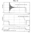
- a voltage waveform and a current waveform of the latter diodes are shown in FIG. 10 .
- a state where a current flows through the diodes is shifted to a state where the current is interrupted and a voltage is applied, carriers stored in the diodes are discharged and a current (reverse recovery current) temporarily flows in a reverse direction. Then, a serge voltage is generated.
- the surge voltage continues to oscillate for a while due to resonance caused by junction capacitance of the diodes and circuit inductance.
- a recovery phenomenon depends on characteristics of diodes.
- the surge voltage is intensely generated as shown in FIG. 10 , the surge voltage may exceed a device withstanding voltage and the devices may be destroyed. Even when the surge voltage does not exceed the device withstanding pressure, an electromagnetic noise of a high frequency may be generated, and accordingly, other electronic devices may be negatively affected. For example, they may be electromagnetically interfered.
- a technique of providing a CR circuit (snubber circuit) in parallel to diodes constituting a rectifier circuit is known.
- a DC-DC converter disclosed in Japanese Patent Laid-Open Publication No. 2006-352959 Patent Document 3
- a device for transmitting electric power disclosed in Japanese Patent Laid-Open Publication No. 2009-273355 Patent Document 4
- a low-loss converter disclosed in Japanese Patent Laid-Open Publication No. 2008-79403 Patent Document 5
- the circuit shown in FIG. 9 as a conventional example has three problems.
- the first problem is how to reduce the surge voltage of the diodes constituting the rectifier circuit 105 during the power recovery.
- the second problem is that it is difficult to recognize a correct load state from the secondary current 12 because the resonant current Iz, which flows through the resonant circuit composed of the resonant capacitor 107 and resonant switch 106 added to reduce the turn-off loss of the converter 102, is superposed on the secondary current 12.
- a current sensor for directly detecting the load current Id may be provided to recognize the correct load state.
- the problem here is, however, how to correctly estimate the load current Id from the secondary current 12 for saving the cost and recognize the correct load state without the current sensor for detecting the load current Id.
- the third problem is how to perform the smooth control when the load is light. Since the amplitude of the resonant current Iz flowing through the resonant capacitor 107 is proportional to a DC input voltage Vs, an energy supplied by the resonant current Iz is proportional to the square of the DC input voltage Vs. When the DC input voltage Vs is high, a considerably high energy is supplied only by the resonant current Iz. Thus, it is difficult to reduce the supplied electric power.
- the DC power supply including a DC voltage source, a converter for converting DC power outputted from the DC voltage source to AC power, a transformer for receiving the AC power outputted from the converter, a rectifier circuit for converting the AC power outputted from the transformer to DC power, a resonant circuit composed of a resonant switch and a resonant capacitor connected in parallel to a DC output side of the rectifier circuit; a filter reactor and filter capacitor for smoothing the DC power outputted from the rectifier circuit, and a load connected in parallel to the filter capacitor, includes: a snubber circuit connected in parallel to the filter capacitor.
- the DC power supply according to the aspect of the present invention further includes: a first voltage sensor for detecting a DC voltage outputted from the DC voltage source; a current sensor for detecting a secondary current of the transformer; a second voltage sensor for detecting a voltage of the filter capacitor; and a controller for adjusting gate pulses of the converter and the resonant switch and detection timings of the first and second voltage sensors and the current sensor.
- the controller may include: first controlling means for inputting output signals of the first and second voltage sensors and the current sensor and adjusting supplied power by adjusting a gate pulse width in accordance with a sensor input while an operating frequency of the converter is maintained constant; and second controlling means for adjusting the supplied power by adjusting the operating frequency of the converter in accordance with the sensor input while the gate pulse width of the converter is maintained constant.
- the snubber circuit may be composed of a diode bridge (snubber diode) and a capacitor (snubber capacitor) for connecting an output of the diode bridge to a DC output side of the rectifier circuit.
- the controller may include means for inputting the output signal of the current sensor and performing sampling and holding in synchronization with the operating frequency of the converter during a period except for 3/4 of a resonant cycle obtained by an electrostatic capacitance of the resonant capacitor and a circuit inductance during turn-on of the converter and 1/2 of a resonant cycle obtained by an electrostatic capacitance of the snubber capacitor and the circuit inductance.
- the surge voltage generated during power recovery of the diodes of the rectifier circuit can be reduced and thus the electromagnetic noise can be also reduced.
- the current sensor for the secondary current of the transformer may be provided and sampling and holding may be performed by inputting an output signal from the current sensor in synchronization with the operating frequency of the converter after 1/2 of the resonant cycle obtained by the electrostatic capacitance of the snubber capacitor and the circuit inductance from turn-on of the converter and before 3/4 of the resonant cycle obtained from the electrostatic capacitance of the resonant capacitor and the circuit inductance from turn-off, the load current can be correctly estimated from the secondary current.
- the supplied power can be reduced when the load is light.
- FIG. 1 shows an embodiment of the present invention.
- a DC power supply shown in FIG. 1 includes: a DC voltage source 100; a first voltage sensor 101 for detecting a DC input voltage Vs as an output voltage of the DC voltage source 100; a converter 102 for converting DC power outputted from the DC voltage source 100 into AC power; a transformer 103 for inputting the AC power outputted from the converter 102; a current sensor 104 for detecting a secondary current 12 of the transformer 103; a rectifier circuit 105 for converting the AC power outputted from the transformer 103 into DC power; a resonant circuit which is composed of a resonant switch 106 and a resonant capacitor 107 and connected in parallel to a DC output side of the rectifier circuit 105; a filter reactor 108 and filter capacitor 112 for smoothing the DC power outputted from the rectifier circuit 105; a snubber diode 110 serving as a diode bridge connected in parallel to the filter capacitor 112; a snubber
- FIG. 2 shows the detail arrangement of the controller 114.
- the controller 114 of the DC power supply shown in FIG. 2 includes: a first A/D converter 200 for inputting an output signal of the second voltage sensor 111; a second A/D converter 201 for inputting an output signal of the current sensor 104; a third A/D converter 202 for inputting an output signal of the first voltage sensor 101; a first subtractor 203 for obtaining a deviation between a DC output voltage command Vd* and a DC output voltage Vd as an output signal of the first A/D converter 200; a first PI controller 204 for inputting an output signal of the first subtractor 203 and outputting a load current command Id*; a second subtractor 205 for obtaining a deviation between the load current command Id* outputted from the first PI controller 204 and a load current estimated value Id' as an output signal of the second A/D converter 201; a second PI controller 208 for inputting an output signal of the second subtractor 205 via an A contact
- the A contact switch 206 and the B contact switch 207 exclusively operate as follows.
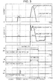
- FIG. 3 shows an operation waveform of the DC power supply according to the present invention.
- the following signals are shown from the top.
- the horizontal axis of FIG. 3 is a time axis.
- the state transitions from [state 1] to [state 5] with the passage of time.
- the sum of the current value of the resonant current Iz and the current value of the snubber current Is is superposed on the current value of the secondary current 12 of the transformer 103, and thus the current value of the secondary current 12 of the transformer 103 is increased once. After 1/2 of the resonant cycle of the resonant capacitor 107, however, the current value of the secondary current 12 is decreased to zero. The secondary current 12 of the transformer 103 does not flow in the negative direction due to the diodes constituting the rectifier circuit 105, and accordingly, the current value of the secondary current 12 continues to zero.
- the turn-off loss of the resonant switch 106 becomes zero because the resonant current Iz flowing through the resonant switch 106 is negative.
- the turn-off loss of the semiconductor devices Q1 to Q4 constituting the converter 102 can be considerably reduced because the primary current I1 of the transformer 103 is composed of only excitation current.
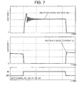
- FIGS. 7 and 10 show an operation waveform of the DC power supply during power recovery according to the present invention.
- the following signals are shown from the top.
- the primary current I1 and the secondary current 12 of the transformer 103 are zero but the free wheeling current continues to flow through the diodes constituting the rectifier circuit 105.
- the semiconductor devices Ql and Q4 are turned on from that state, the primary current I1 and the secondary current 12 of the transformer 103 start to flow and the magnitude of the secondary current 12 of the transformer 103 becomes the same as that of the load current Id.
- a current having the same magnitude as that of the secondary current 12 of the transformer 103 flows through a half of the diodes constituting the rectifier circuit 105 and no current flows through the other half of the diodes.
- a voltage waveform and a current waveform of the latter diodes are shown in FIGS. 7 and 10 .
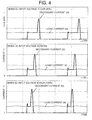
- FIG. 4 shows an example of the operation waveform of the DC power supply according to the present invention.
- FIG. 4 shows a waveform in a mode where the second PI controller 209 shown in FIG. 2 is operating.
- the following signals are shown from the top.
- the turn-on time T1 of the converter 102 is determined in accordance with the ratio of the DC input voltage Vs and the DC output voltage Vd. To control the DC output voltage Vd to be constant, it can be simply considered that the turn-on time T1 of the semiconductor devices constituting the converter 102 is inversely proportional to the magnitude of the DC input voltage Vs. However, the magnitude of the resonant current Iz is proportional to the DC input voltage Vs as shown in FIG. 4 .
- the turn-on time T1 of the semiconductor devices constituting the converter 102 becomes shorter than a value that is inversely proportional to the magnitude of the DC input voltage Vs as the DC input voltage Vs is increased.
- the load current Id is maintained constant by adjusting the turn-on time T1 of the semiconductor devices constituting the converter 102 in accordance with the DC input voltage Vs.
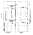
- FIG. 5 shows an example of the operation waveform of the DC power supply according to the present invention.
- FIG. 5 shows a waveform in a mode where the second PI controller 209 shown in FIG. 2 is operating.
- the following signals are shown from the top.
- the turn-on time T1 of the semiconductor devices constituting the converter 102 is constant irrespective of the magnitude of the load current Id. While the converter 102 is on, the load current Id is increased in accordance with the DC input voltage Vs, the DC output voltage Vd, and the inductance of the filter reactor 108. While the converter 102 is off, the load current Id is decreased in accordance with the DC output voltage Vd and the inductance of the filter reactor 108. The state where the increased amount of the load current Id equals to the decreased amount is a steady state.
- the turn-on time T1 of the semiconductor devices constituting the converter 102 does not depend on the magnitude of the load current Id.
- the energy transferred by the resonant current Iz is proportional to the square of the DC input voltage Vs. Accordingly, when the load is light, the turn-on time T1 of the semiconductor devices constituting the converter 102 is required to be shorter than that when the load is rated.
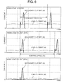
- FIG. 6 shows an example of the operation waveform of the DC power supply according to the present invention.
- the following signals are shown from the top.
- the supplied power is adjusted by controlling the turn-on time T1 of the semiconductor devices constituting the converter 102 to be shorter than that when the load is rated.
- the energy transferred by the resonant current Iz is proportional to the square of the DC input voltage Vs. Accordingly, even when the turn-on time T1 of the semiconductor devices constituting the converter 102 is shortened, the turn-on time T1 cannot be lower than the lower limit value T1min of the turn-on time of the semiconductor devices constituting the converter 102 if the DC input voltage Vs is high. Thus, it is impossible to further reduce the supplied power. At this time, the supplied power can be adjusted by setting the converter control cycle Tc of the converter 102 to be longer.
- FIG. 6 shows a waveform in a mode where the first PI controller 208 shown in FIG. 2 is operating.
- the lower limit value T1min of the turn-on time of the semiconductor devices constituting the converter 102 is required to be larger than the sum of 3/4 of the resonant cycle obtained by the electrostatic capacitance of the resonant capacitor 107 and the circuit inductance and 1/2 of the resonant cycle obtained by the electrostatic capacitance of the snubber capacitor 109 and the circuit inductance.
Landscapes
- Engineering & Computer Science (AREA)
- Power Engineering (AREA)
- Dc-Dc Converters (AREA)
- Rectifiers (AREA)
Abstract
Description
- The present invention relates to a DC power supply using semiconductor devices. More specifically, the present invention relates to a soft-switching DC power supply including a resonant circuit for reducing switching losses in semiconductor devices.
- A power supply for converting direct current to direct current (hereinafter referred to as a DC power supply) is used to stabilize unstable direct current voltage, change direct current voltage, or provide electric isolation between input and output. Especially, in a DC power supply for providing electric isolation between input and output, a method of downsizing an isolation transformer by increasing an applied frequency is known.
-
FIG. 8 shows a circuit configuration disclosed in Japanese Patent Laid-Open Publication No.2010-178501 FIG. 8 includes: aDC voltage source 100; aconverter 102 for converting DC power outputted from theDC voltage source 100 into AC power; atransformer 103 for inputting the AC power outputted from theconverter 102; arectifier circuit 105 for converting the AC power outputted from thetransformer 103 into DC power; afilter reactor 108 andfilter capacitor 112 for smoothing the DC power outputted from therectifier circuit 105; and aload 113 connected in parallel to thefilter capacitor 112. - In the DC power supply shown in
FIG. 8 , switching losses in semiconductor devices composing theconverter 102 are increased in accordance with an applied frequency. Accordingly, a technique (soft-switching) for reducing switching losses using a resonant circuit is suggested.FIG. 9 shows a circuit configuration disclosed in Japanese Patent Laid-Open Publication No.4-368464 - A DC power supply shown in
FIG. 9 includes: aDC voltage source 100; aconverter 102 for converting DC power outputted from theDC voltage source 100 into AC power; atransformer 103 for inputting the AC power outputted from theconverter 102; arectifier circuit 105 for converting the AC power outputted from thetransformer 103 into DC power; a resonant circuit which is composed of aresonant switch 106 and aresonant capacitor 107 and which is connected in parallel to a DC output side of therectifier circuit 105; afilter reactor 108 andfilter capacitor 112 for smoothing the DC power outputted from therectifier circuit 105; and aload 113 connected in parallel to thefilter capacitor 112. - The DC power supply shown in
FIG. 9 activates theresonant switch 106 at the timing of turning off theconverter 102 to superpose a resonant current Iz on asecondary current 12. Accordingly, thesecondary current 12 can be temporarily reduced to zero and a primary current I1 can be temporarily reduced to a level of only excitation current. By turning off theconverter 102 at this timing, the turn-off power loss of theconverter 102 can be considerably reduced. - In the DC power supply shown in
FIG. 8 , while semiconductor devices Q1 to Q4 constituting theconverter 102 are off, the primary current I1 and thesecondary current 12 are zero but a free wheeling current continues to flow through diodes constituting therectifier circuit 105. When the semiconductor devices Q1 and Q4 constituting theconverter 102 are turned on, the primary current I1 and thesecondary current 12 start to flow and the magnitude of thesecondary current 12 matches that of a load current Id. At this time, a current having the same magnitude as that of thesecondary current 12 flows through a half of the diodes constituting therectifier circuit 105 and no current flows through the other half of the diodes. - A voltage waveform and a current waveform of the latter diodes are shown in
FIG. 10 . When a state where a current flows through the diodes is shifted to a state where the current is interrupted and a voltage is applied, carriers stored in the diodes are discharged and a current (reverse recovery current) temporarily flows in a reverse direction. Then, a serge voltage is generated. The surge voltage continues to oscillate for a while due to resonance caused by junction capacitance of the diodes and circuit inductance. A recovery phenomenon depends on characteristics of diodes. When the surge voltage is intensely generated as shown inFIG. 10 , the surge voltage may exceed a device withstanding voltage and the devices may be destroyed. Even when the surge voltage does not exceed the device withstanding pressure, an electromagnetic noise of a high frequency may be generated, and accordingly, other electronic devices may be negatively affected. For example, they may be electromagnetically interfered. - As a countermeasure against a surge voltage during power recovery, a technique of providing a CR circuit (snubber circuit) in parallel to diodes constituting a rectifier circuit is known. As conventional examples of the countermeasure against the surge voltage, a DC-DC converter disclosed in Japanese Patent Laid-Open Publication No.
2006-352959 2009-273355 2008-79403 - The circuit shown in
FIG. 9 as a conventional example has three problems. The first problem is how to reduce the surge voltage of the diodes constituting therectifier circuit 105 during the power recovery. - The second problem is that it is difficult to recognize a correct load state from the
secondary current 12 because the resonant current Iz, which flows through the resonant circuit composed of theresonant capacitor 107 andresonant switch 106 added to reduce the turn-off loss of theconverter 102, is superposed on thesecondary current 12. A current sensor for directly detecting the load current Id may be provided to recognize the correct load state. The problem here is, however, how to correctly estimate the load current Id from thesecondary current 12 for saving the cost and recognize the correct load state without the current sensor for detecting the load current Id. - The third problem is how to perform the smooth control when the load is light. Since the amplitude of the resonant current Iz flowing through the
resonant capacitor 107 is proportional to a DC input voltage Vs, an energy supplied by the resonant current Iz is proportional to the square of the DC input voltage Vs. When the DC input voltage Vs is high, a considerably high energy is supplied only by the resonant current Iz. Thus, it is difficult to reduce the supplied electric power. - To seek to address the first problem, the DC power supply according to an aspect of the present invention including a DC voltage source, a converter for converting DC power outputted from the DC voltage source to AC power, a transformer for receiving the AC power outputted from the converter, a rectifier circuit for converting the AC power outputted from the transformer to DC power, a resonant circuit composed of a resonant switch and a resonant capacitor connected in parallel to a DC output side of the rectifier circuit; a filter reactor and filter capacitor for smoothing the DC power outputted from the rectifier circuit, and a load connected in parallel to the filter capacitor, includes: a snubber circuit connected in parallel to the filter capacitor. To seek to address the second and third problems, the DC power supply according to the aspect of the present invention further includes: a first voltage sensor for detecting a DC voltage outputted from the DC voltage source; a current sensor for detecting a secondary current of the transformer; a second voltage sensor for detecting a voltage of the filter capacitor; and a controller for adjusting gate pulses of the converter and the resonant switch and detection timings of the first and second voltage sensors and the current sensor.
- In the DC power supply according to the aspect of the present invention, the controller may include: first controlling means for inputting output signals of the first and second voltage sensors and the current sensor and adjusting supplied power by adjusting a gate pulse width in accordance with a sensor input while an operating frequency of the converter is maintained constant; and second controlling means for adjusting the supplied power by adjusting the operating frequency of the converter in accordance with the sensor input while the gate pulse width of the converter is maintained constant.
- In the power supply according to the aspect of the present invention, the snubber circuit may be composed of a diode bridge (snubber diode) and a capacitor (snubber capacitor) for connecting an output of the diode bridge to a DC output side of the rectifier circuit. The controller may include means for inputting the output signal of the current sensor and performing sampling and holding in synchronization with the operating frequency of the converter during a period except for 3/4 of a resonant cycle obtained by an electrostatic capacitance of the resonant capacitor and a circuit inductance during turn-on of the converter and 1/2 of a resonant cycle obtained by an electrostatic capacitance of the snubber capacitor and the circuit inductance.
- Due to the option of the snubber circuit composed of the snubber diode serving as the diode bridge connected in parallel to the filter capacitor and the snubber capacitor for connecting an output at an intermediate point of the diode bridge of the snubber diode serving as the diode bridge to the DC output side of the diodes of the rectifier circuit, the surge voltage generated during power recovery of the diodes of the rectifier circuit can be reduced and thus the electromagnetic noise can be also reduced.
- Since the current sensor for the secondary current of the transformer may be provided and sampling and holding may be performed by inputting an output signal from the current sensor in synchronization with the operating frequency of the converter after 1/2 of the resonant cycle obtained by the electrostatic capacitance of the snubber capacitor and the circuit inductance from turn-on of the converter and before 3/4 of the resonant cycle obtained from the electrostatic capacitance of the resonant capacitor and the circuit inductance from turn-off, the load current can be correctly estimated from the secondary current.
- Since the first controlling means for adjusting the supplied power by adjusting the gate pulse width in accordance with the sensor input while the operating frequency of the converter is maintained constant and the second controlling means for adjusting the supplied power by adjusting the operating frequency of the converter in accordance with the sensor input while the gate pulse width of the converter is maintained constant may be provided, the supplied power can be reduced when the load is light.
-
-
FIG. 1 shows a circuit configuration of a DC power supply according to the present invention; -
FIG. 2 shows an internal arrangement of a controller of the DC power supply according to the present invention; -
FIG. 3 shows details of a control timing as an example of an operation waveform according to the present invention; -
FIG. 4 shows adjustments in accordance with a DC input voltage as the example of the operation waveform according to the present invention; -
FIG. 5 shows adjustments in accordance with a load factor as the example of the operation waveform according to the present invention; -
FIG. 6 shows adjustments in accordance with the load factor as the example of the operation waveform according to the present invention; -
FIG. 7 shows a voltage waveform and a current waveform of a rectifier diode according to the present invention; -
FIG. 8 shows a circuit configuration of a DC power supply according to a conventional technique (Patent Document 1); -
FIG. 9 shows a circuit configuration of a DC power supply according to another conventional technique (Patent Document 2 and the like); and -
FIG. 10 shows a voltage waveform and a current waveform of a rectifier diode in the DC power supply according to the conventional technique (Patent Document 1). - Embodiments of the present invention will be explained below with reference to the accompanying drawings.
-
FIG. 1 shows an embodiment of the present invention. A DC power supply shown inFIG. 1 includes: aDC voltage source 100; afirst voltage sensor 101 for detecting a DC input voltage Vs as an output voltage of theDC voltage source 100; aconverter 102 for converting DC power outputted from theDC voltage source 100 into AC power; atransformer 103 for inputting the AC power outputted from theconverter 102; acurrent sensor 104 for detecting asecondary current 12 of thetransformer 103; arectifier circuit 105 for converting the AC power outputted from thetransformer 103 into DC power; a resonant circuit which is composed of aresonant switch 106 and aresonant capacitor 107 and connected in parallel to a DC output side of therectifier circuit 105; afilter reactor 108 andfilter capacitor 112 for smoothing the DC power outputted from therectifier circuit 105; asnubber diode 110 serving as a diode bridge connected in parallel to thefilter capacitor 112; asnubber capacitor 109 for connecting the output at the intermediate point of the diode bridge of thesnubber diode 110 to the DC output side of therectifier circuit 105; asecond voltage sensor 111 for detecting a DC output voltage Vd of thefilter capacitor 112; aload 113 connected in parallel to thefilter capacitor 112; and acontroller 114 for inputting the DC input voltage Vs detected by thefirst voltage sensor 101, the DC output voltage Vd detected by thesecond voltage sensor 111, and thesecondary current 12 detected by thecurrent sensor 104, and controlling gate signals G1 to G4 of semiconductor devices Q1 to Q4 constituting theconverter 102 and a gate signal Gz of a semiconductor device Qz constituting theresonant switch 106. -
FIG. 2 shows the detail arrangement of thecontroller 114. Thecontroller 114 of the DC power supply shown inFIG. 2 includes: a first A/D converter 200 for inputting an output signal of thesecond voltage sensor 111; a second A/D converter 201 for inputting an output signal of thecurrent sensor 104; a third A/D converter 202 for inputting an output signal of thefirst voltage sensor 101; afirst subtractor 203 for obtaining a deviation between a DC output voltage command Vd* and a DC output voltage Vd as an output signal of the first A/D converter 200; afirst PI controller 204 for inputting an output signal of thefirst subtractor 203 and outputting a load current command Id*; asecond subtractor 205 for obtaining a deviation between the load current command Id* outputted from thefirst PI controller 204 and a load current estimated value Id' as an output signal of the second A/D converter 201; asecond PI controller 208 for inputting an output signal of thesecond subtractor 205 via anA contact switch 206; afirst adder 210 for obtaining a converter control cycle Tc by adding an output signal of thesecond PI controller 208 and an initial value Tc* of the converter control cycle; a function table 212 for inputting the DC output voltage Vd as the output signal of the first A/D converter 200 and a DC input voltage Vs as an output signal of the third A/D converter 202 and outputting a turn-on time command T1* of a semiconductor device constituting theconverter 102; athird PI controller 209 for inputting an output signal of thesecond subtractor 205 via aB contact switch 207; asecond adder 211 for obtaining the sum of the output signal of thethird PI controller 209 and the turn-on time command T1* of the semiconductor devices constituting theconverter 102 of the function table 212; alimiter 213 for inputting an output signal of thesecond adder 211, limiting a turn-on time T1 of the semiconductor devices constituting theconverter 102 within a predetermined range, and outputting an underflow flag UF determining whether an output is limited or not; and apulse controller 214 for inputting the control cycle Tc of theconverter 102 outputted from thefirst adder 210, the turn-on time T1 of the semiconductor devices constituting theconverter 102 outputted from thelimiter 213, and a turn-on time T2 of the semiconductor device constituting theresonant switch 106, and outputting gate signals G1 to G4 of semiconductor devices Q1 to Q4 constituting theconverter 102, a gate signal Gz of a semiconductor device Qz constituting theresonant switch 106, and a trigger signal Tad of an A/D converter that samples and holds the first to third A/D converters 200 to 202. - In accordance with the underflow flag UF outputted from the
limiter 213, theA contact switch 206 and theB contact switch 207 exclusively operate as follows. - a) When the output of the
limiter 213 is within a predetermined range (T1 > T1min),
underflow flag UF: off
A contact switch 206: opened
first PI controller 208: reset, zero output first adder 210: output Tc* (fixed)
B contact switch 207: connected
second PI controller 209: operating
limiter 213: output T1 (variable) - b) When the output of the
limiter 213 is limited to a lower limit value (T1 = T1min),
underflow flag UF: on
A contact switch 206: connected
first PI controller 208: operating
first adder 210: output Tc (variable)
B contact switch 207: opened
second PI controller 209: reset, zero output
limiter 213: output T1min (fixed) -
FIG. 3 shows an operation waveform of the DC power supply according to the present invention. InFIG. 3 , the following signals are shown from the top. - (1) the secondary current 12 and the load current Id
- (2) the resonant current Iz and the snubber current Is
- (3) the gate signals G1 and G4 of the semiconductor devices Q1 and Q4 constituting the
converter 102 - (4) the gate signal Gz of the semiconductor device Qz constituting the
resonant switch 106 - (5) the trigger signal Tad of the first to third A/
D converters 200 to 202 - The horizontal axis of
FIG. 3 is a time axis. The state transitions from [state 1] to [state 5] with the passage of time. - [state 1] When the semiconductor devices Q1 and Q4 constituting the
converter 102 are off, the secondary current 12 of thetransformer 103 is zero and the load current Id continue to flow through therectifier circuit 105. - [state 2] When the semiconductor devices Q1 and Q4 constituting the
converter 102 are turned on, the secondary current 12 of thetransformer 103 starts to flow, and simultaneously, the charge current Is of thesnubber capacitor 109 starts to flow. Such a state is continued for approximately half of a resonant cycle obtained by the electrostatic capacitance of thesnubber capacitor 109 and the circuit inductance. - [state 3] When the charging of the
snubber capacitor 109 is finished, the magnitude of the secondary current 12 of thetransformer 103 matches that of the load current Id. At the initial timing of such a state, the trigger signal Tad of the A/D converter for operating the first to third A/D converters is outputted and the A/D conversion (sampling and holding) is performed. Accordingly, the value of the load current Id can be obtained using the detected value of the secondary current 12 of thetransformer 103. - [State 4] Before the semiconductor devices Q1 and Q4 constituting the
converter 102 are turned off, the semiconductor device Qz constituting theresonant switch 106 is turned on at the timing prior to 3/4 of the resonant cycle obtained by the electrostatic capacitance of theresonant capacitor 107 and the circuit inductance. The electric charge charged in thesnubber capacitor 109 is instantly discharged and is charged in theresonant capacitor 107, and subsequently, thesnubber capacitor 109 is recharged. The sum of the current value of the resonant current Iz and the current value of the snubber current Is is superposed on the current value of the secondary current 12 of thetransformer 103, and thus the current value of the secondary current 12 of thetransformer 103 is increased once. After 1/2 of the resonant cycle of theresonant capacitor 107, however, the current value of the secondary current 12 is decreased to zero. The secondary current 12 of thetransformer 103 does not flow in the negative direction due to the diodes constituting therectifier circuit 105, and accordingly, the current value of the secondary current 12 continues to zero. When theresonant switch 106 is turned off while the current value of the secondary current 12 of thetransformer 103 is zero, the turn-off loss of theresonant switch 106 becomes zero because the resonant current Iz flowing through theresonant switch 106 is negative. When theconverter 102 is turned off while the current value of the secondary current 12 of thetransformer 103 is zero, the turn-off loss of the semiconductor devices Q1 to Q4 constituting theconverter 102 can be considerably reduced because the primary current I1 of thetransformer 103 is composed of only excitation current. - [State 5] When the semiconductor devices Q1 and Q4 constituting the
converter 102 are off and the semiconductor device Qz constituting theresonant switch 106 is off, the secondary current 12 of thetransformer 103 is zero, but the resonant current Iz continues to flow until the electric charge charged to theresonant capacitor 107 becomes zero. The sum of the resonant current Iz and the snubber current Is is supplied to theload 113 as the load current Id. When the resonant current Iz becomes zero, the state is retuned back to thestate 1. -
FIGS. 7 and10 show an operation waveform of the DC power supply during power recovery according to the present invention. InFIGS. 7 and10 , the following signals are shown from the top. - (1) the DC output voltage Vd as a terminal voltage of the diodes constituting the
rectifier circuit 105 - (2) the load current Id as a current flowing through the diodes constituting the
rectifier circuit 105 - (3) the gate signals G1 and G4 of the semiconductor devices Q1 and Q4 constituting the
converter 102 - While the semiconductor devices Q1 and Q4 constituting the
converter 102 are off, the primary current I1 and the secondary current 12 of thetransformer 103 are zero but the free wheeling current continues to flow through the diodes constituting therectifier circuit 105. When the semiconductor devices Ql and Q4 are turned on from that state, the primary current I1 and the secondary current 12 of thetransformer 103 start to flow and the magnitude of the secondary current 12 of thetransformer 103 becomes the same as that of the load current Id. At this time, a current having the same magnitude as that of the secondary current 12 of thetransformer 103 flows through a half of the diodes constituting therectifier circuit 105 and no current flows through the other half of the diodes. A voltage waveform and a current waveform of the latter diodes are shown inFIGS. 7 and10 . - When a state where the current flows through the diodes constituting the
rectifier circuit 105 transitions to a state where the current is interrupted and a voltage is applied, carriers stored in the diodes constituting therectifier circuit 105 are discharged and a current (reverse recovery current) flows temporarily in a reverse direction. Then, a serge voltage is generated. As compared to the conventional techniques shown inFIGS. 9 and10 , it is found that the surge voltage can be reduced by the snubber circuit composed of thesnubber capacitor 109 and thesnubber diode 110. -
FIG. 4 shows an example of the operation waveform of the DC power supply according to the present invention.FIG. 4 shows a waveform in a mode where thesecond PI controller 209 shown inFIG. 2 is operating. InFIG. 4 , the following signals are shown from the top. - (1) the secondary current 12 and the load current Id of the
transformer 103 when the DC input voltage Vs is a low voltage (80%) when a load is rated - (2) the secondary current 12 and the load current Id of the
transformer 103 when the DC input voltage Vs is a rated voltage when the load is rated - (3) the secondary current 12 and the load current Id of the
transformer 103 when the DC input voltage Vs is a high voltage (120%) when the load is rated - When the resonant current Iz is not flowing, the turn-on time T1 of the
converter 102 is determined in accordance with the ratio of the DC input voltage Vs and the DC output voltage Vd. To control the DC output voltage Vd to be constant, it can be simply considered that the turn-on time T1 of the semiconductor devices constituting theconverter 102 is inversely proportional to the magnitude of the DC input voltage Vs. However, the magnitude of the resonant current Iz is proportional to the DC input voltage Vs as shown inFIG. 4 . Since the energy transferred by the resonant current Iz is proportional to the square of the DC input voltage Vs, the turn-on time T1 of the semiconductor devices constituting theconverter 102 becomes shorter than a value that is inversely proportional to the magnitude of the DC input voltage Vs as the DC input voltage Vs is increased. When the load is rated, the load current Id is maintained constant by adjusting the turn-on time T1 of the semiconductor devices constituting theconverter 102 in accordance with the DC input voltage Vs. -
FIG. 5 shows an example of the operation waveform of the DC power supply according to the present invention.FIG. 5 shows a waveform in a mode where thesecond PI controller 209 shown inFIG. 2 is operating. InFIG. 5 , the following signals are shown from the top. - (1) the secondary current 12 of the
transformer 103 and the load current Id when the DC input voltage Vs is a rated voltage when a load is rated - (2) the secondary current 12 of the
transformer 103 and the load current Id when the DC input voltage Vs is the rated voltage when a load is light (50%) - When the resonant current Iz does not flow, the turn-on time T1 of the semiconductor devices constituting the
converter 102 is constant irrespective of the magnitude of the load current Id. While theconverter 102 is on, the load current Id is increased in accordance with the DC input voltage Vs, the DC output voltage Vd, and the inductance of thefilter reactor 108. While theconverter 102 is off, the load current Id is decreased in accordance with the DC output voltage Vd and the inductance of thefilter reactor 108. The state where the increased amount of the load current Id equals to the decreased amount is a steady state. The turn-on time T1 of the semiconductor devices constituting theconverter 102 does not depend on the magnitude of the load current Id. - The energy transferred by the resonant current Iz is proportional to the square of the DC input voltage Vs. Accordingly, when the load is light, the turn-on time T1 of the semiconductor devices constituting the
converter 102 is required to be shorter than that when the load is rated. -
FIG. 6 shows an example of the operation waveform of the DC power supply according to the present invention. InFIG. 6 , the following signals are shown from the top. - (1) the secondary current 12 of the
transformer 103 and the load current Id when the DC input voltage Vs is a high voltage (120%) when a load is rated - (2) the secondary current 12 of the
transformer 103 and the load current Id when the DC input voltage Vs is a high voltage (120%) when a load is light (50%) - (3) the secondary current 12 of the
transformer 103 and the load current Id when the DC input voltage Vs is a high voltage (120%) when a load is light (20%) - When the load becomes light, the supplied power is adjusted by controlling the turn-on time T1 of the semiconductor devices constituting the
converter 102 to be shorter than that when the load is rated. The energy transferred by the resonant current Iz is proportional to the square of the DC input voltage Vs. Accordingly, even when the turn-on time T1 of the semiconductor devices constituting theconverter 102 is shortened, the turn-on time T1 cannot be lower than the lower limit value T1min of the turn-on time of the semiconductor devices constituting theconverter 102 if the DC input voltage Vs is high. Thus, it is impossible to further reduce the supplied power. At this time, the supplied power can be adjusted by setting the converter control cycle Tc of theconverter 102 to be longer.FIG. 6 shows a waveform in a mode where thefirst PI controller 208 shown inFIG. 2 is operating. - To secure a period for sampling and holding the first to third A/
D converters 200 to 202, the lower limit value T1min of the turn-on time of the semiconductor devices constituting theconverter 102 is required to be larger than the sum of 3/4 of the resonant cycle obtained by the electrostatic capacitance of theresonant capacitor 107 and the circuit inductance and 1/2 of the resonant cycle obtained by the electrostatic capacitance of thesnubber capacitor 109 and the circuit inductance. 100: DC voltage source - 101: first voltage sensor
- 102: converter
- 103: transformer
- 104: current sensor
- 105: rectifier circuit
- 106: resonant switch
- 107: resonant capacitor
- 108: filter reactor
- 109: snubber capacitor
- 110: snubber diode
- 111: second voltage sensor
- 112: filter capacitor
- 113: load
- 114: controller
- 200: first A/D converter
- 201: second A/D converter
- 202: third A/D converter
- 203: first subtractor
- 204: first PI controller
- 205: second subtractor
- 206: A contact switch
- 207: B contact switch
- 208: second PI controller
- 209: third PI controller
- 210: first adder
- 211: second adder
- 212: function table
- 213: limiter
- 214: pulse controller
- G1 to G4: gate signals of the semiconductor devices Q1 to Q4 constituting the
converter 102 - Gz: gate signal of the semiconductor device Qz constituting the
resonant switch 106 - I1: primary current
- 12: secondary current
- Id: load current
- Id*: load current command
- Id': load current estimated value
- Ir: rectifier diode current
- Is: snubber current
- Iz: resonant current
- T1: turn-on time of the semiconductor device constituting the
converter 102 - T1min: lower limit value of the turn-on time of the semiconductor device constituting the
converter 102 - T1*: turn-on time command of the semiconductor device constituting the
converter 102 - T2: turn-on time of the semiconductor device constituting the
resonant switch 106 - Tad: trigger signal of the A/D converter
- Tc*: initial value of the converter control cycle
- Tc: converter control cycle
- Q1 to Q4: semiconductor devices constituting the
converter 102 - Qz: semiconductor device constituting the
resonant switch 106 - UF: underflow flag
- Vd*: DC output voltage command
- Vd: DC output voltage
- Vr: rectifier diode voltage
- Vs: DC input voltage
Claims (7)
- A DC power supply including a DC voltage source, a converter for converting DC power outputted from the DC voltage source to AC power, a transformer for inputting the AC power outputted from the converter, a rectifier circuit for converting the AC power outputted from the transformer to DC power; a resonant circuit composed of a resonant switch and a resonant capacitor connected in parallel to a DC output side of the rectifier circuit; a filter reactor and a filter capacitor for smoothing the DC power outputted from the rectifier circuit, a snubber circuit connected in parallel to the filter capacitor, and a load connected in parallel to the filter capacitor, the DC power supply comprising:a first voltage sensor for detecting an output voltage of the DC voltage source;a second voltage sensor for detecting a voltage of the filter capacitor;a current sensor for detecting an input current or an output current of the transformer; anda controller for inputting output signals of the first voltage sensor, second voltage sensor, and current sensor, and outputting a signal that controls a gate pulse of a plurality of semiconductor devices constituting the converter and a gate pulse of a semiconductor device constituting the resonant switch and a signal that adjusts detection timings of the first voltage sensor, second voltage sensor, and current sensor.
- The DC power supply according to claim 1, wherein the snubber circuit includes a diode bridge of a snubber diode and a snubber capacitor for connecting an output of the snubber diode and a DC output side of the rectifier circuit.
- The DC power supply according to claim 1, wherein the controller for the gate pulse includes: first controlling means for adjusting supplied power by adjusting a gate pulse width in accordance with a sensor input while an operating frequency of the converter is maintained constant; and second controlling means for adjusting the supplied power by adjusting the operating frequency of the converter in accordance with the sensor input while the gate pulse width of the converter is maintained constant.
- The DC power supply according to claim 3, wherein the gate pulse width of the converter has a predetermined lower limit value and means for switching between the first controlling means and the second controlling means based on the lower limit value is provided.
- The DC power supply according to claim 4, wherein the lower limit value of the gate pulse width of the converter is set to be larger than a sum of 3/4 of a resonant cycle obtained by an electrostatic capacitance of the resonant capacitor and a circuit inductance and 1/2 of a resonant cycle obtained by an electrostatic capacitance of the snubber capacitor and the circuit inductance.
- The DC power supply according to claim 2, wherein the controller for controlling the gate signal includes means for inputting an output signal of the current sensor and performing sampling and holding in synchronization with an operating frequency of the converter after 1/2 of a resonant cycle obtained by an electrostatic capacitance of the snubber capacitor and a circuit inductance from turn-on of the converter and before 3/4 of a resonant cycle obtained by an electrostatic capacitance of the resonant capacitor and the circuit inductance from turn-off.
- The DC power supply according to claim 2, wherein the controller for controlling the gate signal includes: first controlling means for adjusting supplied power by adjusting a gate pulse width in accordance with a sensor input while an operating frequency of the converter is maintained constant; second controlling means for adjusting the supplied power by adjusting the operating frequency of the converter in accordance with the sensor input while the gate pulse width of the converter is maintained constant; means for switching between the first controlling means and the second controlling means based on a lower limit value that is larger than a sum of 3/4 of a resonant cycle obtained by an electrostatic capacitance of the resonant capacitor and a circuit inductance and 1/2 of a resonant cycle obtained by an electrostatic capacitance of the snubber capacitor and the circuit inductance; and means for inputting an output signal of the current sensor and performing sampling and holding in synchronization with an operating frequency of the converter after 1/2 of the resonant cycle obtained by the electrostatic capacitance of the snubber capacitor and the circuit inductance from turn-on of the converter and before 3/4 of the resonant cycle obtained by the electrostatic capacitance of the resonant capacitor and the circuit inductance from turn-off.
Applications Claiming Priority (1)
| Application Number | Priority Date | Filing Date | Title |
|---|---|---|---|
| JP2011116758A JP5690654B2 (en) | 2011-05-25 | 2011-05-25 | DC power supply |
Publications (3)
| Publication Number | Publication Date |
|---|---|
| EP2528218A2 true EP2528218A2 (en) | 2012-11-28 |
| EP2528218A3 EP2528218A3 (en) | 2015-09-09 |
| EP2528218B1 EP2528218B1 (en) | 2018-01-10 |
Family
ID=46197053
Family Applications (1)
| Application Number | Title | Priority Date | Filing Date |
|---|---|---|---|
| EP12169273.5A Not-in-force EP2528218B1 (en) | 2011-05-25 | 2012-05-24 | DC power supply |
Country Status (5)
| Country | Link |
|---|---|
| US (1) | US8964414B2 (en) |
| EP (1) | EP2528218B1 (en) |
| JP (1) | JP5690654B2 (en) |
| KR (1) | KR101333980B1 (en) |
| CN (1) | CN102801327B (en) |
Cited By (4)
| Publication number | Priority date | Publication date | Assignee | Title |
|---|---|---|---|---|
| EP2814165A3 (en) * | 2013-03-29 | 2015-09-23 | Hitachi, Ltd. | DC Power Supply |
| EP2779401A3 (en) * | 2013-03-15 | 2015-10-21 | Hitachi, Ltd. | DC Power Supply |
| EP2848452A3 (en) * | 2013-09-13 | 2015-11-04 | Hitachi Ltd. | Traction converter system |
| EP3324528A1 (en) * | 2016-11-21 | 2018-05-23 | Siemens Aktiengesellschaft | Direct current converter and method for its operation |
Families Citing this family (32)
| Publication number | Priority date | Publication date | Assignee | Title |
|---|---|---|---|---|
| US11131431B2 (en) | 2014-09-28 | 2021-09-28 | Jiaxing Super Lighting Electric Appliance Co., Ltd | LED tube lamp |
| JP5935891B2 (en) * | 2012-08-29 | 2016-06-15 | 富士通株式会社 | Power supply device and control method of power supply device |
| DE102012219365A1 (en) * | 2012-10-23 | 2014-04-24 | Schmidhauser Ag | DC converter |
| CN105144562B (en) | 2013-05-21 | 2017-10-31 | 株式会社村田制作所 | Switching power unit |
| KR101500079B1 (en) | 2013-05-30 | 2015-03-06 | 현대자동차주식회사 | Method for Estimating Current of DC-DC converter |
| KR20150049962A (en) * | 2013-10-31 | 2015-05-08 | 삼성전기주식회사 | Power supply apparatus and controlling method thereof |
| US9350260B2 (en) * | 2013-11-07 | 2016-05-24 | Futurewei Technologies, Inc. | Startup method and system for resonant converters |
| KR20160020099A (en) * | 2014-08-13 | 2016-02-23 | 주식회사 솔루엠 | Power conveter and driving method for the same |
| US11480305B2 (en) | 2014-09-25 | 2022-10-25 | Jiaxing Super Lighting Electric Appliance Co., Ltd. | LED tube lamp |
| US10560989B2 (en) | 2014-09-28 | 2020-02-11 | Jiaxing Super Lighting Electric Appliance Co., Ltd | LED tube lamp |
| US12638141B2 (en) | 2014-09-28 | 2026-05-26 | Jiaxing Super Lighting Electric Appliance Co., Ltd | LED tube lamp |
| WO2016045630A1 (en) | 2014-09-28 | 2016-03-31 | Jiaxing Super Lighting Electric Appliance Co., Ltd | Led tube lamp |
| JP6161834B2 (en) * | 2014-10-22 | 2017-07-12 | 三菱電機株式会社 | Auxiliary power supply for electric cars |
| KR101597461B1 (en) * | 2014-11-14 | 2016-02-25 | 인하대학교 산학협력단 | LED Current Estimation Circuit Using the Time Information for LED Driver |
| US11519565B2 (en) | 2015-03-10 | 2022-12-06 | Jiaxing Super Lighting Electric Appliance Co., Ltd | LED lamp and its power source module |
| US9897265B2 (en) | 2015-03-10 | 2018-02-20 | Jiaxing Super Lighting Electric Appliance Co., Ltd. | LED tube lamp having LED light strip |
| US10075083B2 (en) * | 2015-04-02 | 2018-09-11 | Virginia Tech Intellectual Properties, Inc. | Multi-step simplified optimal trajectory control (SOTC) based on only Vo and I load |
| JP6502158B2 (en) * | 2015-04-24 | 2019-04-17 | ローム株式会社 | Switching power supply |
| JP6004555B1 (en) | 2015-09-11 | 2016-10-12 | Hoya Candeo Optronics株式会社 | Switching power supply device and light irradiation device including the same |
| EP3365967B1 (en) * | 2015-10-23 | 2019-08-21 | OSRAM GmbH | Electronic converter and related method of operating an electronic converter |
| CN105391291B (en) * | 2015-11-26 | 2018-03-16 | 华为技术有限公司 | A kind of power circuit |
| EP3340448B1 (en) * | 2016-12-23 | 2023-06-07 | Delta Electronics (Thailand) Public Co., Ltd. | Electric power converter with snubber circuit |
| JP2019017231A (en) * | 2017-07-11 | 2019-01-31 | Tdk株式会社 | Electronic apparatus |
| JP6963930B2 (en) * | 2017-08-07 | 2021-11-10 | 株式会社Gsユアサ インフラシステムズ | DC / DC converter |
| KR102453825B1 (en) * | 2017-10-18 | 2022-10-13 | 현대자동차주식회사 | Dc-dc converter |
| US10797609B2 (en) | 2019-02-26 | 2020-10-06 | Analog Devices International Unlimited Company | Systems and methods for transferring power across an isolation barrier using an active self synchronized rectifier |
| US10790754B2 (en) | 2019-02-26 | 2020-09-29 | Analog Devices International Unlimited Company | Systems and methods for transferring power across an isolation barrier using an active resonator |
| JP7276005B2 (en) * | 2019-08-29 | 2023-05-18 | 富士電機株式会社 | Snubber circuit and power converter |
| CN219283098U (en) | 2021-01-27 | 2023-06-30 | 嘉兴山蒲照明电器有限公司 | A kind of LED straight tube lamp |
| KR102741910B1 (en) * | 2022-12-27 | 2024-12-16 | 한국전자기술연구원 | Power imbalance prevention circuit and method of resonance type power converter |
| CN118801540B (en) * | 2024-09-10 | 2024-12-06 | 泉州装备制造研究所 | Multi-device constant-voltage wireless charging system with adjustable output power |
| CN120879965B (en) * | 2025-09-24 | 2025-12-05 | 泉州维盾电气有限公司 | High-voltage electricity-taking capacitor protection and harmonic suppression system and circuit thereof |
Citations (5)
| Publication number | Priority date | Publication date | Assignee | Title |
|---|---|---|---|---|
| JPH04368464A (en) | 1991-06-12 | 1992-12-21 | Sanyo Denki Co Ltd | Dc power source |
| JP2006352959A (en) | 2005-06-14 | 2006-12-28 | Fuji Electric Systems Co Ltd | DC-DC converter |
| JP2008079403A (en) | 2006-09-20 | 2008-04-03 | Kawamura Electric Inc | Low loss converter |
| JP2009273355A (en) | 2008-05-06 | 2009-11-19 | Siemens Ag | Apparatus for transmitting electric power |
| JP2010178501A (en) | 2009-01-29 | 2010-08-12 | Fuji Electric Systems Co Ltd | Power conversion device |
Family Cites Families (22)
| Publication number | Priority date | Publication date | Assignee | Title |
|---|---|---|---|---|
| US5657215A (en) * | 1995-08-29 | 1997-08-12 | Compaq Computer Corporation | Controlling switch-Mode power conversion |
| JPH0978465A (en) * | 1995-09-13 | 1997-03-25 | Osamu Katayama | Elastic skin materials such as shoes and bags |
| JPH09285126A (en) * | 1996-04-18 | 1997-10-31 | Fuji Electric Co Ltd | Snubber circuit of semiconductor rectifier |
| KR100199506B1 (en) * | 1996-10-29 | 1999-06-15 | 윤문수 | A zero voltage/current switching circuit for reduced ripple current of the full-bridge dc/dc converter |
| US5877947A (en) * | 1997-07-30 | 1999-03-02 | Lucent Technologies Inc. | Snubber circuit for a rectifier and method of operation thereof |
| JPH1198836A (en) * | 1997-09-10 | 1999-04-09 | Korea Electrotechnol Inst | Circuit for zero voltage / zero current switching of full bridge DC / DC converter capable of reducing ripple of output current |
| JPH11187662A (en) * | 1997-12-24 | 1999-07-09 | Isuzu Motors Ltd | DC-DC converter |
| US6349044B1 (en) * | 1999-09-09 | 2002-02-19 | Virginia Tech Intellectual Properties, Inc. | Zero voltage zero current three level dc-dc converter |
| JP4167811B2 (en) * | 2001-03-05 | 2008-10-22 | Tdk株式会社 | Switching power supply |
| US6504739B2 (en) * | 2001-05-18 | 2003-01-07 | Astec International Limited | Simple control circuit for synchronous rectifiers used in ZVS phase shifted full bridge converter |
| ITTO20020782A1 (en) * | 2002-09-06 | 2004-03-07 | Fiat Ricerche | DC-DC CONVERTER. |
| AT501998B1 (en) * | 2003-08-20 | 2008-06-15 | Siemens Ag Oesterreich | SWITCHING REGULATOR |
| US6906931B1 (en) * | 2004-01-30 | 2005-06-14 | Astec International Limited | Zero-voltage switching half-bridge DC-DC converter topology by utilizing the transformer leakage inductance trapped energy |
| US7173404B2 (en) * | 2004-08-11 | 2007-02-06 | Niko Semiconductor Co., Ltd. | Auto-switching converter with PWM and PFM selection |
| JP2007068349A (en) * | 2005-08-31 | 2007-03-15 | Tdk Corp | Switching power supply |
| JP4899528B2 (en) * | 2006-02-24 | 2012-03-21 | セイコーエプソン株式会社 | Power supply |
| JP4618339B2 (en) * | 2008-06-20 | 2011-01-26 | ミツミ電機株式会社 | DC-DC converter |
| CN101795076B (en) | 2009-01-29 | 2015-04-15 | 富士电机株式会社 | Power converter and method for controlling power converter |
| KR101155698B1 (en) * | 2009-02-06 | 2012-06-12 | 신덴겐코교 가부시키가이샤 | Current detecting circuit and transformer current measuring system |
| JP2011041387A (en) * | 2009-08-10 | 2011-02-24 | Fuji Electric Systems Co Ltd | Dc-dc conversion circuit |
| CN101630906B (en) * | 2009-08-20 | 2011-11-16 | 旭曜科技股份有限公司 | DC-DC Transformer and OLED Display with PWM and PFM Automatic Switching |
| US8811046B2 (en) * | 2010-06-30 | 2014-08-19 | Marvell World Trade Ltd. | Primary side voltage control in flyback converter |
-
2011
- 2011-05-25 JP JP2011116758A patent/JP5690654B2/en not_active Expired - Fee Related
-
2012
- 2012-05-21 CN CN201210158567.2A patent/CN102801327B/en not_active Expired - Fee Related
- 2012-05-24 EP EP12169273.5A patent/EP2528218B1/en not_active Not-in-force
- 2012-05-24 KR KR1020120055376A patent/KR101333980B1/en not_active Expired - Fee Related
- 2012-05-25 US US13/480,503 patent/US8964414B2/en active Active
Patent Citations (5)
| Publication number | Priority date | Publication date | Assignee | Title |
|---|---|---|---|---|
| JPH04368464A (en) | 1991-06-12 | 1992-12-21 | Sanyo Denki Co Ltd | Dc power source |
| JP2006352959A (en) | 2005-06-14 | 2006-12-28 | Fuji Electric Systems Co Ltd | DC-DC converter |
| JP2008079403A (en) | 2006-09-20 | 2008-04-03 | Kawamura Electric Inc | Low loss converter |
| JP2009273355A (en) | 2008-05-06 | 2009-11-19 | Siemens Ag | Apparatus for transmitting electric power |
| JP2010178501A (en) | 2009-01-29 | 2010-08-12 | Fuji Electric Systems Co Ltd | Power conversion device |
Non-Patent Citations (1)
| Title |
|---|
| 0. DEBLECKER; A. MORETTI; F. VALLEE: "Comparative Analysis of Two zero-Current Switching Isolated DC-DC Converters for Auxiliary Railway Supply", SPEEDAM, 2008 |
Cited By (6)
| Publication number | Priority date | Publication date | Assignee | Title |
|---|---|---|---|---|
| EP2779401A3 (en) * | 2013-03-15 | 2015-10-21 | Hitachi, Ltd. | DC Power Supply |
| EP2814165A3 (en) * | 2013-03-29 | 2015-09-23 | Hitachi, Ltd. | DC Power Supply |
| EP2848452A3 (en) * | 2013-09-13 | 2015-11-04 | Hitachi Ltd. | Traction converter system |
| EP3324528A1 (en) * | 2016-11-21 | 2018-05-23 | Siemens Aktiengesellschaft | Direct current converter and method for its operation |
| WO2018091299A1 (en) * | 2016-11-21 | 2018-05-24 | Siemens Aktiengesellschaft | Dc-dc converter and method for operating same |
| US10566909B2 (en) | 2016-11-21 | 2020-02-18 | Siemens Aktiengesellschaft | DC-DC converter and method for operating same |
Also Published As
| Publication number | Publication date |
|---|---|
| EP2528218A3 (en) | 2015-09-09 |
| JP5690654B2 (en) | 2015-03-25 |
| CN102801327B (en) | 2015-01-07 |
| KR101333980B1 (en) | 2013-11-27 |
| JP2012249351A (en) | 2012-12-13 |
| US8964414B2 (en) | 2015-02-24 |
| EP2528218B1 (en) | 2018-01-10 |
| US20120300501A1 (en) | 2012-11-29 |
| KR20120132384A (en) | 2012-12-05 |
| CN102801327A (en) | 2012-11-28 |
Similar Documents
| Publication | Publication Date | Title |
|---|---|---|
| EP2528218B1 (en) | DC power supply | |
| US10892687B2 (en) | Asymmetric power converter, power converters, and operating power converters | |
| JP7378495B2 (en) | Power converters and respective control devices with active non-dissipative clamp circuits | |
| US7499295B2 (en) | Switch mode power supply controllers | |
| EP3346596B1 (en) | Symmetric time shift control for resonant converters | |
| CN105981279B (en) | Current resonance type dc voltage changer, control integrated circuit and current resonance type DC voltage transforming method | |
| US7592790B2 (en) | Start-up circuit with feedforward compensation for power converters | |
| CN111327196B (en) | Synchronizing multiple controllers in a power converter | |
| TWI664801B (en) | Switching power, control apparatus and control method | |
| EP2707942B1 (en) | Switching delay controller for a switched mode power supply | |
| CN104980050A (en) | System and Method for Switched-Mode Power Supply | |
| US9136769B2 (en) | Load change detection for switched mode power supply with low no load power | |
| CN101495934A (en) | Forward power converter and controller | |
| KR20130035925A (en) | Multi-stage sampling circuit for a power converter controller | |
| KR101542645B1 (en) | On time sampling prevention | |
| EP2887520A1 (en) | A synchronous rectifier and a method for controlling it | |
| CN108696132A (en) | control device and control method | |
| TWI445291B (en) | Methods and power controllers for primary side control | |
| US9184663B2 (en) | Switching power supply device | |
| US20140078787A1 (en) | Switching power source device | |
| Liu et al. | Real-time adaptive timing control of synchronous rectifiers in high frequency GaN LLC converter | |
| US7248487B1 (en) | Switch mode power supply controllers | |
| US8929102B2 (en) | Sample and hold buffer | |
| US20020114174A1 (en) | Power supply unit and driving method thereof | |
| US11742774B2 (en) | Switch driving device and switching power supply using the same |
Legal Events
| Date | Code | Title | Description |
|---|---|---|---|
| PUAI | Public reference made under article 153(3) epc to a published international application that has entered the european phase |
Free format text: ORIGINAL CODE: 0009012 |
|
| 17P | Request for examination filed |
Effective date: 20120611 |
|
| AK | Designated contracting states |
Kind code of ref document: A2 Designated state(s): AL AT BE BG CH CY CZ DE DK EE ES FI FR GB GR HR HU IE IS IT LI LT LU LV MC MK MT NL NO PL PT RO RS SE SI SK SM TR |
|
| AX | Request for extension of the european patent |
Extension state: BA ME |
|
| PUAL | Search report despatched |
Free format text: ORIGINAL CODE: 0009013 |
|
| AK | Designated contracting states |
Kind code of ref document: A3 Designated state(s): AL AT BE BG CH CY CZ DE DK EE ES FI FR GB GR HR HU IE IS IT LI LT LU LV MC MK MT NL NO PL PT RO RS SE SI SK SM TR |
|
| AX | Request for extension of the european patent |
Extension state: BA ME |
|
| RIC1 | Information provided on ipc code assigned before grant |
Ipc: H02M 3/335 20060101AFI20150806BHEP |
|
| 17Q | First examination report despatched |
Effective date: 20160711 |
|
| GRAP | Despatch of communication of intention to grant a patent |
Free format text: ORIGINAL CODE: EPIDOSNIGR1 |
|
| INTG | Intention to grant announced |
Effective date: 20170801 |
|
| GRAS | Grant fee paid |
Free format text: ORIGINAL CODE: EPIDOSNIGR3 |
|
| GRAA | (expected) grant |
Free format text: ORIGINAL CODE: 0009210 |
|
| AK | Designated contracting states |
Kind code of ref document: B1 Designated state(s): AL AT BE BG CH CY CZ DE DK EE ES FI FR GB GR HR HU IE IS IT LI LT LU LV MC MK MT NL NO PL PT RO RS SE SI SK SM TR |
|
| REG | Reference to a national code |
Ref country code: GB Ref legal event code: FG4D |
|
| REG | Reference to a national code |
Ref country code: CH Ref legal event code: EP Ref country code: AT Ref legal event code: REF Ref document number: 963471 Country of ref document: AT Kind code of ref document: T Effective date: 20180115 |
|
| REG | Reference to a national code |
Ref country code: IE Ref legal event code: FG4D |
|
| REG | Reference to a national code |
Ref country code: DE Ref legal event code: R096 Ref document number: 602012041763 Country of ref document: DE |
|
| REG | Reference to a national code |
Ref country code: NL Ref legal event code: MP Effective date: 20180110 |
|
| REG | Reference to a national code |
Ref country code: AT Ref legal event code: MK05 Ref document number: 963471 Country of ref document: AT Kind code of ref document: T Effective date: 20180110 |
|
| PG25 | Lapsed in a contracting state [announced via postgrant information from national office to epo] |
Ref country code: NL Free format text: LAPSE BECAUSE OF FAILURE TO SUBMIT A TRANSLATION OF THE DESCRIPTION OR TO PAY THE FEE WITHIN THE PRESCRIBED TIME-LIMIT Effective date: 20180110 |
|
| PG25 | Lapsed in a contracting state [announced via postgrant information from national office to epo] |
Ref country code: HR Free format text: LAPSE BECAUSE OF FAILURE TO SUBMIT A TRANSLATION OF THE DESCRIPTION OR TO PAY THE FEE WITHIN THE PRESCRIBED TIME-LIMIT Effective date: 20180110 Ref country code: LT Free format text: LAPSE BECAUSE OF FAILURE TO SUBMIT A TRANSLATION OF THE DESCRIPTION OR TO PAY THE FEE WITHIN THE PRESCRIBED TIME-LIMIT Effective date: 20180110 Ref country code: CY Free format text: LAPSE BECAUSE OF FAILURE TO SUBMIT A TRANSLATION OF THE DESCRIPTION OR TO PAY THE FEE WITHIN THE PRESCRIBED TIME-LIMIT Effective date: 20180110 Ref country code: ES Free format text: LAPSE BECAUSE OF FAILURE TO SUBMIT A TRANSLATION OF THE DESCRIPTION OR TO PAY THE FEE WITHIN THE PRESCRIBED TIME-LIMIT Effective date: 20180110 Ref country code: NO Free format text: LAPSE BECAUSE OF FAILURE TO SUBMIT A TRANSLATION OF THE DESCRIPTION OR TO PAY THE FEE WITHIN THE PRESCRIBED TIME-LIMIT Effective date: 20180410 Ref country code: FI Free format text: LAPSE BECAUSE OF FAILURE TO SUBMIT A TRANSLATION OF THE DESCRIPTION OR TO PAY THE FEE WITHIN THE PRESCRIBED TIME-LIMIT Effective date: 20180110 |
|
| PG25 | Lapsed in a contracting state [announced via postgrant information from national office to epo] |
Ref country code: LV Free format text: LAPSE BECAUSE OF FAILURE TO SUBMIT A TRANSLATION OF THE DESCRIPTION OR TO PAY THE FEE WITHIN THE PRESCRIBED TIME-LIMIT Effective date: 20180110 Ref country code: AT Free format text: LAPSE BECAUSE OF FAILURE TO SUBMIT A TRANSLATION OF THE DESCRIPTION OR TO PAY THE FEE WITHIN THE PRESCRIBED TIME-LIMIT Effective date: 20180110 Ref country code: PL Free format text: LAPSE BECAUSE OF FAILURE TO SUBMIT A TRANSLATION OF THE DESCRIPTION OR TO PAY THE FEE WITHIN THE PRESCRIBED TIME-LIMIT Effective date: 20180110 Ref country code: BG Free format text: LAPSE BECAUSE OF FAILURE TO SUBMIT A TRANSLATION OF THE DESCRIPTION OR TO PAY THE FEE WITHIN THE PRESCRIBED TIME-LIMIT Effective date: 20180410 Ref country code: GR Free format text: LAPSE BECAUSE OF FAILURE TO SUBMIT A TRANSLATION OF THE DESCRIPTION OR TO PAY THE FEE WITHIN THE PRESCRIBED TIME-LIMIT Effective date: 20180411 Ref country code: RS Free format text: LAPSE BECAUSE OF FAILURE TO SUBMIT A TRANSLATION OF THE DESCRIPTION OR TO PAY THE FEE WITHIN THE PRESCRIBED TIME-LIMIT Effective date: 20180110 Ref country code: IS Free format text: LAPSE BECAUSE OF FAILURE TO SUBMIT A TRANSLATION OF THE DESCRIPTION OR TO PAY THE FEE WITHIN THE PRESCRIBED TIME-LIMIT Effective date: 20180510 Ref country code: SE Free format text: LAPSE BECAUSE OF FAILURE TO SUBMIT A TRANSLATION OF THE DESCRIPTION OR TO PAY THE FEE WITHIN THE PRESCRIBED TIME-LIMIT Effective date: 20180110 |
|
| REG | Reference to a national code |
Ref country code: DE Ref legal event code: R097 Ref document number: 602012041763 Country of ref document: DE |
|
| PG25 | Lapsed in a contracting state [announced via postgrant information from national office to epo] |
Ref country code: AL Free format text: LAPSE BECAUSE OF FAILURE TO SUBMIT A TRANSLATION OF THE DESCRIPTION OR TO PAY THE FEE WITHIN THE PRESCRIBED TIME-LIMIT Effective date: 20180110 Ref country code: RO Free format text: LAPSE BECAUSE OF FAILURE TO SUBMIT A TRANSLATION OF THE DESCRIPTION OR TO PAY THE FEE WITHIN THE PRESCRIBED TIME-LIMIT Effective date: 20180110 Ref country code: EE Free format text: LAPSE BECAUSE OF FAILURE TO SUBMIT A TRANSLATION OF THE DESCRIPTION OR TO PAY THE FEE WITHIN THE PRESCRIBED TIME-LIMIT Effective date: 20180110 |
|
| PLBE | No opposition filed within time limit |
Free format text: ORIGINAL CODE: 0009261 |
|
| STAA | Information on the status of an ep patent application or granted ep patent |
Free format text: STATUS: NO OPPOSITION FILED WITHIN TIME LIMIT |
|
| PG25 | Lapsed in a contracting state [announced via postgrant information from national office to epo] |
Ref country code: SM Free format text: LAPSE BECAUSE OF FAILURE TO SUBMIT A TRANSLATION OF THE DESCRIPTION OR TO PAY THE FEE WITHIN THE PRESCRIBED TIME-LIMIT Effective date: 20180110 Ref country code: DK Free format text: LAPSE BECAUSE OF FAILURE TO SUBMIT A TRANSLATION OF THE DESCRIPTION OR TO PAY THE FEE WITHIN THE PRESCRIBED TIME-LIMIT Effective date: 20180110 Ref country code: CZ Free format text: LAPSE BECAUSE OF FAILURE TO SUBMIT A TRANSLATION OF THE DESCRIPTION OR TO PAY THE FEE WITHIN THE PRESCRIBED TIME-LIMIT Effective date: 20180110 Ref country code: SK Free format text: LAPSE BECAUSE OF FAILURE TO SUBMIT A TRANSLATION OF THE DESCRIPTION OR TO PAY THE FEE WITHIN THE PRESCRIBED TIME-LIMIT Effective date: 20180110 |
|
| REG | Reference to a national code |
Ref country code: CH Ref legal event code: PL |
|
| 26N | No opposition filed |
Effective date: 20181011 |
|
| REG | Reference to a national code |
Ref country code: BE Ref legal event code: MM Effective date: 20180531 |
|
| PG25 | Lapsed in a contracting state [announced via postgrant information from national office to epo] |
Ref country code: MC Free format text: LAPSE BECAUSE OF FAILURE TO SUBMIT A TRANSLATION OF THE DESCRIPTION OR TO PAY THE FEE WITHIN THE PRESCRIBED TIME-LIMIT Effective date: 20180110 |
|
| REG | Reference to a national code |
Ref country code: IE Ref legal event code: MM4A |
|
| PG25 | Lapsed in a contracting state [announced via postgrant information from national office to epo] |
Ref country code: CH Free format text: LAPSE BECAUSE OF NON-PAYMENT OF DUE FEES Effective date: 20180531 Ref country code: LI Free format text: LAPSE BECAUSE OF NON-PAYMENT OF DUE FEES Effective date: 20180531 Ref country code: SI Free format text: LAPSE BECAUSE OF FAILURE TO SUBMIT A TRANSLATION OF THE DESCRIPTION OR TO PAY THE FEE WITHIN THE PRESCRIBED TIME-LIMIT Effective date: 20180110 |
|
| PG25 | Lapsed in a contracting state [announced via postgrant information from national office to epo] |
Ref country code: LU Free format text: LAPSE BECAUSE OF NON-PAYMENT OF DUE FEES Effective date: 20180524 |
|
| PG25 | Lapsed in a contracting state [announced via postgrant information from national office to epo] |
Ref country code: IE Free format text: LAPSE BECAUSE OF NON-PAYMENT OF DUE FEES Effective date: 20180524 Ref country code: FR Free format text: LAPSE BECAUSE OF NON-PAYMENT OF DUE FEES Effective date: 20180531 |
|
| PG25 | Lapsed in a contracting state [announced via postgrant information from national office to epo] |
Ref country code: BE Free format text: LAPSE BECAUSE OF NON-PAYMENT OF DUE FEES Effective date: 20180531 |
|
| PG25 | Lapsed in a contracting state [announced via postgrant information from national office to epo] |
Ref country code: MT Free format text: LAPSE BECAUSE OF NON-PAYMENT OF DUE FEES Effective date: 20180524 |
|
| PG25 | Lapsed in a contracting state [announced via postgrant information from national office to epo] |
Ref country code: TR Free format text: LAPSE BECAUSE OF FAILURE TO SUBMIT A TRANSLATION OF THE DESCRIPTION OR TO PAY THE FEE WITHIN THE PRESCRIBED TIME-LIMIT Effective date: 20180110 |
|
| PG25 | Lapsed in a contracting state [announced via postgrant information from national office to epo] |
Ref country code: PT Free format text: LAPSE BECAUSE OF FAILURE TO SUBMIT A TRANSLATION OF THE DESCRIPTION OR TO PAY THE FEE WITHIN THE PRESCRIBED TIME-LIMIT Effective date: 20180110 Ref country code: HU Free format text: LAPSE BECAUSE OF FAILURE TO SUBMIT A TRANSLATION OF THE DESCRIPTION OR TO PAY THE FEE WITHIN THE PRESCRIBED TIME-LIMIT; INVALID AB INITIO Effective date: 20120524 |
|
| PG25 | Lapsed in a contracting state [announced via postgrant information from national office to epo] |
Ref country code: MK Free format text: LAPSE BECAUSE OF NON-PAYMENT OF DUE FEES Effective date: 20180110 |
|
| PGFP | Annual fee paid to national office [announced via postgrant information from national office to epo] |
Ref country code: IT Payment date: 20220412 Year of fee payment: 11 Ref country code: GB Payment date: 20220401 Year of fee payment: 11 Ref country code: DE Payment date: 20220329 Year of fee payment: 11 |
|
| REG | Reference to a national code |
Ref country code: DE Ref legal event code: R119 Ref document number: 602012041763 Country of ref document: DE |
|
| GBPC | Gb: european patent ceased through non-payment of renewal fee |
Effective date: 20230524 |
|
| PG25 | Lapsed in a contracting state [announced via postgrant information from national office to epo] |
Ref country code: IT Free format text: LAPSE BECAUSE OF NON-PAYMENT OF DUE FEES Effective date: 20230524 Ref country code: DE Free format text: LAPSE BECAUSE OF NON-PAYMENT OF DUE FEES Effective date: 20231201 Ref country code: GB Free format text: LAPSE BECAUSE OF NON-PAYMENT OF DUE FEES Effective date: 20230524 |