EP2527946A1 - Current limitation for LDO - Google Patents
Current limitation for LDO Download PDFInfo
- Publication number
- EP2527946A1 EP2527946A1 EP11368013A EP11368013A EP2527946A1 EP 2527946 A1 EP2527946 A1 EP 2527946A1 EP 11368013 A EP11368013 A EP 11368013A EP 11368013 A EP11368013 A EP 11368013A EP 2527946 A1 EP2527946 A1 EP 2527946A1
- Authority
- EP
- European Patent Office
- Prior art keywords
- current
- transistor
- pass transistor
- voltage
- source
- Prior art date
- Legal status (The legal status is an assumption and is not a legal conclusion. Google has not performed a legal analysis and makes no representation as to the accuracy of the status listed.)
- Granted
Links
Images

Classifications
-
- G—PHYSICS
- G05—CONTROLLING; REGULATING
- G05F—SYSTEMS FOR REGULATING ELECTRIC OR MAGNETIC VARIABLES
- G05F1/00—Automatic systems in which deviations of an electric quantity from one or more predetermined values are detected at the output of the system and fed back to a device within the system to restore the detected quantity to its predetermined value or values, i.e. retroactive systems
- G05F1/10—Regulating voltage or current
- G05F1/46—Regulating voltage or current wherein the variable actually regulated by the final control device is DC
- G05F1/56—Regulating voltage or current wherein the variable actually regulated by the final control device is DC using semiconductor devices in series with the load as final control devices
- G05F1/565—Regulating voltage or current wherein the variable actually regulated by the final control device is DC using semiconductor devices in series with the load as final control devices sensing a condition of the system or its load in addition to means responsive to deviations in the output of the system, e.g. current, voltage, power factor
- G05F1/569—Regulating voltage or current wherein the variable actually regulated by the final control device is DC using semiconductor devices in series with the load as final control devices sensing a condition of the system or its load in addition to means responsive to deviations in the output of the system, e.g. current, voltage, power factor for protection
- G05F1/573—Regulating voltage or current wherein the variable actually regulated by the final control device is DC using semiconductor devices in series with the load as final control devices sensing a condition of the system or its load in addition to means responsive to deviations in the output of the system, e.g. current, voltage, power factor for protection with overcurrent detector
Definitions
- the circuit invented also comprises a second PMOS pass transistor, wherein its drain is connected to the drain of said first pass transistor, its gate is connected to the gate of said first pass transistor and to the gate of a first PMOS transistor in a diode configuration, and its source is connected to a first means providing resistance and to the source of a second PMOS transistor, said first means providing resistance, wherein its first terminal is connected to VDD voltage and a second terminal is connected to the source of said second PMOS pass transistor, and said first PMOS transistor in a diode configuration, wherein its source is connected to VDD voltage and its drain is connected to its gate and to a first terminal of said means to control said first pass transistor.
Landscapes
- Engineering & Computer Science (AREA)
- Physics & Mathematics (AREA)
- Electromagnetism (AREA)
- General Physics & Mathematics (AREA)
- Radar, Positioning & Navigation (AREA)
- Automation & Control Theory (AREA)
- Continuous-Control Power Sources That Use Transistors (AREA)
Abstract
Description
- This invention relates generally to voltage regulators, and more particularly to low dropout (LDO) having a clipping of the output current.
- Low-dropout (LDO) linear regulators are commonly used to provide power to low-voltage digital and analog circuits, where point-of-load and line regulation is important.
Fig. 1 prior art shows a typical basic circuit of aLDO regulator 4 having aninput voltage V i 1, anoutput voltage V o 2, an input current Ii and an output current Io. - In order to prevent high current stress of the LDO's pass device, especially during start-up, it is important to limit the output current.
- There are various patents disclosed to limit the output current of an LDO or correspondingly to limit the drive current of a pass device of an LDO:
-
U. S. Patent (5,929,617 to Brokaw ) teaches an low dropout voltage regulator (LDO) drive reduction circuit detecting when the LDO's output voltage is going out of regulation due to a falling input voltage while the output is lightly loaded, and reduces the drive to the pass transistor in response. This action prevents the LDO's ground current from rising unnecessarily. The drive reduction circuitry directly monitors the voltage across the pass transistor; when above a predetermined threshold voltage which is typically well-below the LDO's specified dropout voltage, the pass transistor drive is permitted to vary as necessary to maintain a specified output voltage. If the monitored voltage falls below the threshold voltage, indicating that the input voltage is falling and the output is lightly loaded, the drive reduction circuit reduces the drive current, which would otherwise get increased in an attempt to restore the output voltage. The transconductance of the novel drive reduction circuit is relatively high, making the region over which the drive reduction circuit is active small and permitting the threshold voltage to be precisely set. -
U. S. Patent (6,518,737 to Stanescu et al. ) discloses a low dropout voltage regulator with non-Miller frequency compensation. The LDO circuit has two wide-band, low-power cascaded operational transconductance amplifiers (OTAs): an error amplifier and a unity-gain-configured voltage follower. The unity-gain-configured voltage follower drives a gate of a power PMOS path transistor with a high parasitic gate capacitance. The wide-band, low-power OTAs enable the use of a single, low-value load capacitor with a low equivalent series resistance (ESR). A frequency compensation capacitor is connected in parallel with the upper resistor of a feedback network, which introduces a zero-pole pair that enhances the phase margin close to unity-loop-gain frequency. -
U. S. Patent (6,703,813 to Vladislav et al. ) discloses an LDO regulator being arranged to provide regulation with a pass device, a cascode device, a level shifter, an error amplifier, and a tracking voltage divider. The error amplifier is arranged to sense the output voltage and provide an error signal to the pass device via the level shifter. The level shifter changes the DC level of the error signal such that the pass device is isolated from damaging voltages. The cascode device is arranged to increase the impedance between the output node and the pass transistor such that the LDO regulator can sustain input voltages that exceed process limits without damage. The cascode device is biased by the tracking voltage divider. The tracking voltage divider adjusts the biasing to the cascode device such that a decreased input voltages result in lower impedance, and increased input voltages result in higher impedance. - A principal object of the present invention is to limit the output load current of a current driven LDO.
- A further object of the present invention is to limit high current stress of the LDO's pass device especially during start-up.
- A further object of the present invention is achieving a precise current limitation.
- Moreover an object of the invention is to use part of the pass devices to measure the output current.
- In accordance with the object of this invention a circuit to limit the output load current of a current driven LDO voltage regulator, wherein said LDO voltage regulator comprises at least an error amplifier, a first pass transistor, a means to control said pass transistor using the output of said error amplifier and a feedback mechanism to feed a measure of the output voltage back to said error amplifier has been achieved. The circuit invented also comprises a second PMOS pass transistor, wherein its drain is connected to the drain of said first pass transistor, its gate is connected to the gate of said first pass transistor and to the gate of a first PMOS transistor in a diode configuration, and its source is connected to a first means providing resistance and to the source of a second PMOS transistor, said first means providing resistance, wherein its first terminal is connected to VDD voltage and a second terminal is connected to the source of said second PMOS pass transistor, and said first PMOS transistor in a diode configuration, wherein its source is connected to VDD voltage and its drain is connected to its gate and to a first terminal of said means to control said first pass transistor. Furthermore the circuit invented comprises said second PMOS transistor in a diode configuration, wherein its gate is connected to its drain and to the gate of a third PMOS transistor, its source is connected to a second terminal of a second means providing resistance, and its drain is connected to a first terminal of a first current source, said first current source wherein its second terminal is connected to Vss voltage, and said third PMOS transistor wherein its source is connected to the source of said second pass transistor and its drain is connected to a first terminal of a second current source and to a gate of a first NMOS transistor. Finally the circuit comprises said first NMOS transistor, wherein its source is connected to VSS voltage and its drain is connected to a second terminal of said means to control said first pass transistor, said second means providing resistance, wherein its first terminal is connected to VDD voltage, and said second current source wherein its second terminal is connected to Vss voltage.
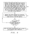
- In accordance with the objects of the invention a method to limit the output load current of a current driven LDO voltage regulator has been achieved. The method invented comprises, first, (1) to provide a current driven LDO voltage regulator structure, an additional second pass transistor, wherein the second pass transistor is smaller than a first pass transistor by a factor K1, a first and a second current source, wherein the first current source generates a current I1 and the second current source generates a current 12, a first resistor and a second resistor, wherein the first resistor is smaller than the second resistor by a factor K2, a current mirror and a first and a second transistor. The following steps of the method are (2) to measure the current through the second pass transistor which is linearly correlated to the output current of the LDO regulator, (3) a check, if current measured in previous step is smaller than a reference current, and, if so, go to step (2) otherwise go to step (4), and (4) limit the current controlling the gate voltage of the two parallel pass transistors.
- In the accompanying drawings forming a material part of this description, there is shown:
-
Fig. 1 prior art illustrates the principal currents of an LDO. -
Fig. 2 shows a schematic of an LDO and a circuitry limiting the output current -
Fig. 3 shows a flowchart of a method to limit the output current of a current driven LDO voltage regulator. - The preferred embodiments disclose circuits and a method to limit the output current in a standard LDO structure. The present invention prevents high current stress of the LDO's pass device, especially during start-up.
-
Fig. 2 shows a standard LDO structure with a preferred embodiment of the circuitry of the present invention. - The LDO shown comprises an
error amplifier 20 having as inputs a reference voltage VREF and the feedback voltage VFB from thevoltage divider 21, comprising resistors R1 and R2. VOUT is the output voltage of the LDO. In the preferred embodiment R1 matches R2; thevoltage divider 21 is used to provide a feedback voltage, representing the output voltage VOUT, to theerror amplifier 20 in order to set the output voltage VOUT to a specified voltage. - Transistors P1, P2, P3, P4, and P5 are PMOS transistors. Transistors P1 and P2 are used in a diode configuration. Transistor P4 has been added in parallel to pass device P5 in order to form a pass device together, wherein P4 is also used to measure the current I3. Transistor P4 matches transistor P5, this means P4 has the same device characteristics as P5, but transistor P4 has a smaller size than P5. Transistor P4 is K1-times smaller than P5.
- Transistor P2 matches Transistor P3 and in the preferred embodiment has the same size.
- The current source 22 generates current I1; the
current source 23 generates current I2. In the preferred embodiment the current I1 equals I2. - Measuring the current I3 through transistor P4 enables the limitation of the output current of the LDO lout. The current I3 is K1-times smaller as the output current IOUT through the pass device P5:

- The current through the voltage divider can be neglected when the current limit retroaction is active.
- The means of resistance R3 matches means of resistance R4. R3 and R4 could be implemented as resistors or transistors. Both resistors R3 and R4 are used to compare current I1 with current I3. Resistor R1 matches R2 and both are used to set the LDO output voltage to a specified value. The control of the limitation of the output current IOUT of the LDO is performed at first by measuring the current I3 through transistor P4, wherein, as mentioned above, the current 13 is K1-times smaller than the current IOUT through transistor P5. The measurement of current I3 is done by regulating the gate voltage of N2 according to the difference between I3 and I1. The current through transistor P1 is mirrored to both pass transistors P4 and P5. Thus the output current IOUT is controlled.
- Transistors P2 and P3 work as a current comparator in regard of
currents current source 23 has a current 12 = I3/K2. - The current I3 through transistor P4 can increase as long as current I3 < K2 × I1, wherein K2=R4/R3. If I3 < K2 × I1 then voltage V2 is smaller than voltage V1, and consequently voltage V3 increases. Since voltage V3 is regulating the gate of NMOS transistor N2, current I3 can increase and a higher output current can be generated, if required.
- The current I3 through transistor P4 is forced to decrease as long as current I3 > K2 × I1. If I3 > K2 × I1 then voltage V2 is larger than voltage V1, and consequently voltage V3 decreases, thus decreasing the current through PMOS transistor N2.
- Using the regulation loop as described above the output current through pass transistor P5 will be limited to IOUT = I1 x K1 x K2.
-
Fig. 3 shows a flowchart of the method of the present invention to limit the output load current of a current driven LDO voltage regulator. Thefirst step 30 describes the provision a current driven LDO voltage regulator structure, an additional second pass transistor, wherein the second pass transistor is smaller than a first pass transistor by a factor K1, a first and a second current source, wherein the first current source generates a current I1 and the second current source generates a current 12, a first resistor and a second resistor, wherein the first resistor is smaller than the second resistor by a factor K2, a current mirror and a first and a second transistor.Step 31 describes the measurement of the current through the second pass transistor, which is flowing through said first resistor and which is linearly correlated to the output current of the LDO regulator.Step 32 comprises a check if the current measured in the previous step is smaller than a reference current. As described above, this reference current is I1*K2. In case the current through the second pass transistor measured is smaller than the reference current, the process flow is going back to step 31 otherwise the process flow goes to step 33 illustrating limiting the current controlling the gate voltage of the two parallel pass transistors. - While the invention has been particularly shown and described with reference to the preferred embodiments thereof, it will be understood by those skilled in the art that various changes in form and details may be made without departing from the spirit and scope of the invention.
Claims (14)
- A circuit to limit the output load current of a current driven LDO voltage regulator, wherein said LDO voltage regulator comprises at least an error amplifier, a first pass transistor, a means to control said pass transistor using the output of said error amplifier and a feedback mechanism to feed a measure of the output voltage back to said error amplifier, is comprising:- a second PMOS pass transistor, wherein its drain is connected to the drain of said first pass transistor, its gate is connected to the gate of said first pass transistor and to the gate of a first PMOS transistor in a diode configuration, and its source is connected to a first means providing resistance and to the source of a second PMOS transistor;- said first means providing resistance, wherein its first terminal is connected to VDD voltage and a second terminal is connected to the source of said second PMOS pass transistor;- said first PMOS transistor in a diode configuration, wherein its source is connected to VDD voltage and its drain is connected to its gate and to a first terminal of said means to control said first pass transistor;- said second PMOS transistor in a diode configuration, wherein its gate is connected to its drain and to the gate of a third PMOS transistor, its source is connected to a second terminal of a second means providing resistance, and its drain is connected to a first terminal of a first current source;- said first current source wherein its second terminal is connected to VSS voltage; said third PMOS transistor wherein its source is connected to the source of said second pass transistor and its drain is connected to a first terminal of a second current source and to a gate of a first NMOS transistor;- said first NMOS transistor, wherein its source is connected to VSS voltage and its drain is connected to a second terminal of said means to control said first pass transistor;- said second means providing resistance, wherein its first terminal is connected to VDD voltage; and- said second current source wherein its second terminal is connected to VSS voltage.
- The circuit of claim 1 wherein said means to control said first pass transistor is an NMOS transistor.
- The circuit of claim 1 wherein said first means to provide resistance is a resistor.
- The circuit of claim 1 wherein said first means to provide resistance is a transistor.
- The circuit of claim 1 wherein said second means to provide resistance is a resistor.
- The circuit of claim 1 wherein said second means to provide resistance is a transistor.
- The circuit of claim 1 wherein said first means to provide resistance is smaller in resistance than said second means to provide resistance.
- The circuit of claim 1 wherein said circuit to limit the output load current of a current driven LDO voltage regulator is integrated on a chip.
- The circuit of claim 1 wherein said second pass transistor is smaller in size than said first pass transistor.
- A method to limit the output load current of a current driven LDO voltage regulator is comprising:(1) providing a current driven LDO voltage regulator structure, an additional second pass transistor, wherein the second pass transistor is smaller than a first pass transistor by a factor K1, a first and a second current source, wherein the first current source generates a current 11 and the second current source generates a current 12, a first resistor and a second resistor, wherein the first resistor is smaller than the second resistor by a factor K2, a current mirror and a first and a second transistor;(2) measuring the current through the second pass transistor, which is flowing through said first resistor and which is linearly correlated to the output current of the LDO regulator;(3) if current measured in previous step is smaller than a reference current go to step (2) otherwise go to step (4); and(4) limit the current controlling the gate voltage of the two parallel pass transistors.
- The method of claim 10 wherein said output load current is limited by regulating the gate voltage of said pass transistors by a voltage which increases if the current through said second pass transistor is larger than the reference current.
- The method of claim 11 wherein said gate voltage is increased by said current mirror if the current through said second pass transistor is larger than the reference current.
- The method of claim 12 wherein said current mirror is a PMOS current mirror.
- The method of claim 12 wherein the output current lout will be limited to lout = I1xK1xK2.
Priority Applications (2)
| Application Number | Priority Date | Filing Date | Title |
|---|---|---|---|
| EP11368013.6A EP2527946B1 (en) | 2011-04-13 | 2011-04-13 | Current limitation for low dropout (LDO) voltage regulator |
| US13/066,604 US8508199B2 (en) | 2011-04-13 | 2011-04-19 | Current limitation for LDO |
Applications Claiming Priority (1)
| Application Number | Priority Date | Filing Date | Title |
|---|---|---|---|
| EP11368013.6A EP2527946B1 (en) | 2011-04-13 | 2011-04-13 | Current limitation for low dropout (LDO) voltage regulator |
Publications (2)
| Publication Number | Publication Date |
|---|---|
| EP2527946A1 true EP2527946A1 (en) | 2012-11-28 |
| EP2527946B1 EP2527946B1 (en) | 2013-12-18 |
Family
ID=47005945
Family Applications (1)
| Application Number | Title | Priority Date | Filing Date |
|---|---|---|---|
| EP11368013.6A Active EP2527946B1 (en) | 2011-04-13 | 2011-04-13 | Current limitation for low dropout (LDO) voltage regulator |
Country Status (2)
| Country | Link |
|---|---|
| US (1) | US8508199B2 (en) |
| EP (1) | EP2527946B1 (en) |
Families Citing this family (28)
| Publication number | Priority date | Publication date | Assignee | Title |
|---|---|---|---|---|
| JP6006913B2 (en) * | 2010-11-19 | 2016-10-12 | ミツミ電機株式会社 | Current limiting circuit and power supply circuit |
| US8878510B2 (en) * | 2012-05-15 | 2014-11-04 | Cadence Ams Design India Private Limited | Reducing power consumption in a voltage regulator |
| US9075422B2 (en) * | 2012-05-31 | 2015-07-07 | Nxp B.V. | Voltage regulator circuit with adaptive current limit and method for operating the voltage regulator circuit |
| JP2014164702A (en) * | 2013-02-27 | 2014-09-08 | Seiko Instruments Inc | Voltage regulator |
| WO2014191787A1 (en) * | 2013-05-29 | 2014-12-04 | Freescale Semiconductor, Inc. | Voltage regulator, application-specific integrated circuit and method for providing a load with a regulated voltage |
| US9465055B2 (en) | 2013-09-26 | 2016-10-11 | Infineon Technologies Ag | Electronic circuit and method for measuring a load current |
| EP2876521B1 (en) * | 2013-11-26 | 2016-05-25 | Dialog Semiconductor GmbH | Circuit with Controlled Inrush Current |
| EP2887174B1 (en) * | 2013-12-20 | 2021-01-13 | Dialog Semiconductor GmbH | CC-CV method to control the startup current for LDO |
| US9429971B2 (en) * | 2014-08-06 | 2016-08-30 | Texas Instruments Incorporated | Short-circuit protection for voltage regulators |
| US9983607B2 (en) * | 2014-11-04 | 2018-05-29 | Microchip Technology Incorporated | Capacitor-less low drop-out (LDO) regulator |
| DE102015205359B4 (en) | 2015-03-24 | 2018-01-25 | Dialog Semiconductor (Uk) Limited | RESTRAIN LIMIT FOR A LOW DROPOUT CONTROLLER IN A DROPOUT CONDITION |
| TWI569123B (en) * | 2015-03-26 | 2017-02-01 | 晨星半導體股份有限公司 | High efficiency low dropout linear regulator |
| JP6624979B2 (en) * | 2016-03-15 | 2019-12-25 | エイブリック株式会社 | Voltage regulator |
| TWI667563B (en) * | 2017-04-10 | 2019-08-01 | 聯華電子股份有限公司 | Voltage regulating circuit |
| JP2019139445A (en) | 2018-02-08 | 2019-08-22 | ローム株式会社 | regulator |
| TWI666538B (en) * | 2018-04-24 | 2019-07-21 | 瑞昱半導體股份有限公司 | Voltage regulator and voltage regulating method |
| JP2020042478A (en) * | 2018-09-10 | 2020-03-19 | キオクシア株式会社 | Semiconductor integrated circuit |
| US10666192B2 (en) * | 2018-09-27 | 2020-05-26 | Qualcomm Incorporated | Attenuation of flicker noise in bias generators |
| US10838444B1 (en) | 2019-07-25 | 2020-11-17 | Semiconductor Components Industries, Llc | Adaptive constant current engine |
| US11217992B2 (en) | 2019-09-20 | 2022-01-04 | Texas Instruments Incorporated | High-speed short-to-ground protection circuit for pass field-effect transistor (FET) |
| US11467613B2 (en) * | 2020-07-15 | 2022-10-11 | Semiconductor Components Industries, Llc | Adaptable low dropout (LDO) voltage regulator and method therefor |
| US11378993B2 (en) * | 2020-09-23 | 2022-07-05 | Microsoft Technology Licensing, Llc | Voltage regulator circuit with current limiter stage |
| CN116529686A (en) * | 2020-12-01 | 2023-08-01 | 艾迈斯传感器比利时有限责任公司 | Low dropout regulator with inrush current limiting capability |
| US12093064B2 (en) | 2021-08-20 | 2024-09-17 | Semiconductor Components Industries, Llc | Wide input voltage range low-power charge pump based LDO |
| US12166417B2 (en) * | 2021-12-17 | 2024-12-10 | Qualcomm Incorporated | Nonlinear current mirror for fast transient and low power regulator |
| US12204354B2 (en) | 2023-04-24 | 2025-01-21 | Texas Instruments Incorporated | Cascode voltage regulator circuit |
| US20250132729A1 (en) * | 2023-10-24 | 2025-04-24 | Cirrus Logic International Semiconductor Ltd. | Output current-dependent voltage regulator output stage reconfiguration |
| CN117519395A (en) * | 2023-12-19 | 2024-02-06 | 圣邦微电子(北京)股份有限公司 | A current limiting circuit applied to LDO |
Citations (8)
| Publication number | Priority date | Publication date | Assignee | Title |
|---|---|---|---|---|
| US4851953A (en) * | 1987-10-28 | 1989-07-25 | Linear Technology Corporation | Low voltage current limit loop |
| US5929617A (en) | 1998-03-03 | 1999-07-27 | Analog Devices, Inc. | LDO regulator dropout drive reduction circuit and method |
| US6246221B1 (en) * | 2000-09-20 | 2001-06-12 | Texas Instruments Incorporated | PMOS low drop-out voltage regulator using non-inverting variable gain stage |
| US6518737B1 (en) | 2001-09-28 | 2003-02-11 | Catalyst Semiconductor, Inc. | Low dropout voltage regulator with non-miller frequency compensation |
| US6703813B1 (en) | 2002-10-24 | 2004-03-09 | National Semiconductor Corporation | Low drop-out voltage regulator |
| US7405546B2 (en) * | 2005-01-28 | 2008-07-29 | Atmel Corporation | Standard CMOS low-noise high PSRR low drop-out regulator with new dynamic compensation |
| US20090309559A1 (en) * | 2008-06-17 | 2009-12-17 | Degang Xia | Automatically configurable dual regulator type circuits and methods |
| WO2011006979A1 (en) * | 2009-07-16 | 2011-01-20 | St-Ericsson (Grenoble) Sas | Low-dropout regulator |
Family Cites Families (6)
| Publication number | Priority date | Publication date | Assignee | Title |
|---|---|---|---|---|
| JP2002091584A (en) * | 2000-09-19 | 2002-03-29 | Rohm Co Ltd | Electrical equipment |
| US6690147B2 (en) * | 2002-05-23 | 2004-02-10 | Texas Instruments Incorporated | LDO voltage regulator having efficient current frequency compensation |
| US7615977B2 (en) * | 2006-05-15 | 2009-11-10 | Stmicroelectronics S.A. | Linear voltage regulator and method of limiting the current in such a regulator |
| JP4929043B2 (en) * | 2007-05-15 | 2012-05-09 | 株式会社リコー | Overcurrent protection circuit and electronic device provided with the overcurrent protection circuit |
| US8174251B2 (en) * | 2007-09-13 | 2012-05-08 | Freescale Semiconductor, Inc. | Series regulator with over current protection circuit |
| US7710090B1 (en) * | 2009-02-17 | 2010-05-04 | Freescale Semiconductor, Inc. | Series regulator with fold-back over current protection circuit |
-
2011
- 2011-04-13 EP EP11368013.6A patent/EP2527946B1/en active Active
- 2011-04-19 US US13/066,604 patent/US8508199B2/en active Active
Patent Citations (8)
| Publication number | Priority date | Publication date | Assignee | Title |
|---|---|---|---|---|
| US4851953A (en) * | 1987-10-28 | 1989-07-25 | Linear Technology Corporation | Low voltage current limit loop |
| US5929617A (en) | 1998-03-03 | 1999-07-27 | Analog Devices, Inc. | LDO regulator dropout drive reduction circuit and method |
| US6246221B1 (en) * | 2000-09-20 | 2001-06-12 | Texas Instruments Incorporated | PMOS low drop-out voltage regulator using non-inverting variable gain stage |
| US6518737B1 (en) | 2001-09-28 | 2003-02-11 | Catalyst Semiconductor, Inc. | Low dropout voltage regulator with non-miller frequency compensation |
| US6703813B1 (en) | 2002-10-24 | 2004-03-09 | National Semiconductor Corporation | Low drop-out voltage regulator |
| US7405546B2 (en) * | 2005-01-28 | 2008-07-29 | Atmel Corporation | Standard CMOS low-noise high PSRR low drop-out regulator with new dynamic compensation |
| US20090309559A1 (en) * | 2008-06-17 | 2009-12-17 | Degang Xia | Automatically configurable dual regulator type circuits and methods |
| WO2011006979A1 (en) * | 2009-07-16 | 2011-01-20 | St-Ericsson (Grenoble) Sas | Low-dropout regulator |
Non-Patent Citations (1)
| Title |
|---|
| GARY PACE KAI ZHONG: "LOW DROPOUT VOLTAGE REGULATOR WITH HIGH STABILITY OUTPUT CURRENT LIMIT CIRCUIT", IP.COM JOURNAL, IP.COM INC., WEST HENRIETTA, NY, US, 16 July 2002 (2002-07-16), XP013003822, ISSN: 1533-0001 * |
Also Published As
| Publication number | Publication date |
|---|---|
| EP2527946B1 (en) | 2013-12-18 |
| US8508199B2 (en) | 2013-08-13 |
| US20120262137A1 (en) | 2012-10-18 |
Similar Documents
| Publication | Publication Date | Title |
|---|---|---|
| EP2527946B1 (en) | Current limitation for low dropout (LDO) voltage regulator | |
| EP3408724B1 (en) | Low dropout voltage regulator with improved power supply rejection and corresponding method | |
| EP1378808B1 (en) | LDO regulator with wide output load range and fast internal loop | |
| US8344713B2 (en) | LDO linear regulator with improved transient response | |
| EP2952996B1 (en) | A current sink stage for LDO | |
| US7893670B2 (en) | Frequency compensation scheme for stabilizing the LDO using external NPN in HV domain | |
| US7397226B1 (en) | Low noise, low power, fast startup, and low drop-out voltage regulator | |
| EP2668549B1 (en) | Voltage regulator having current and voltage foldback based upon load impedance | |
| KR102188206B1 (en) | Voltage regulator | |
| US7782041B1 (en) | Linear regulator for use with electronic circuits | |
| US11507120B2 (en) | Load current based dropout control for continuous regulation in linear regulators | |
| EP2454643B1 (en) | Low-dropout regulator | |
| EP4281840B1 (en) | Low-power voltage regulator with fast transient response | |
| EP1635239A1 (en) | Adaptive biasing concept for current mode voltage regulators | |
| EP2354881A1 (en) | Domino voltage regulator (DVR) | |
| KR102187403B1 (en) | Voltage regulator | |
| US7907003B2 (en) | Method for improving power-supply rejection | |
| CN101223488A (en) | Standard CMOS Low Noise High PSRR Low Dropout Regulator with New Dynamic Compensation | |
| EP1947544A1 (en) | Voltage regulator and method for voltage regulation | |
| US20160161961A1 (en) | Circuit to improve load transient behavior of voltage regulators and load switches | |
| US10768650B1 (en) | Voltage regulator with capacitance multiplier | |
| US10382030B2 (en) | Apparatus having process, voltage and temperature-independent line transient management | |
| KR20100096014A (en) | Voltage Regulator | |
| US7602161B2 (en) | Voltage regulator with inherent voltage clamping | |
| KR102390730B1 (en) | Overcurrent protection circuit and voltage regulator |
Legal Events
| Date | Code | Title | Description |
|---|---|---|---|
| PUAI | Public reference made under article 153(3) epc to a published international application that has entered the european phase |
Free format text: ORIGINAL CODE: 0009012 |
|
| AK | Designated contracting states |
Kind code of ref document: A1 Designated state(s): AL AT BE BG CH CY CZ DE DK EE ES FI FR GB GR HR HU IE IS IT LI LT LU LV MC MK MT NL NO PL PT RO RS SE SI SK SM TR |
|
| AX | Request for extension of the european patent |
Extension state: BA ME |
|
| GRAP | Despatch of communication of intention to grant a patent |
Free format text: ORIGINAL CODE: EPIDOSNIGR1 |
|
| 17P | Request for examination filed |
Effective date: 20130528 |
|
| RBV | Designated contracting states (corrected) |
Designated state(s): AL AT BE BG CH CY CZ DE DK EE ES FI FR GB GR HR HU IE IS IT LI LT LU LV MC MK MT NL NO PL PT RO RS SE SI SK SM TR |
|
| INTG | Intention to grant announced |
Effective date: 20130627 |
|
| RIC1 | Information provided on ipc code assigned before grant |
Ipc: G05F 1/573 20060101AFI20130614BHEP |
|
| GRAS | Grant fee paid |
Free format text: ORIGINAL CODE: EPIDOSNIGR3 |
|
| GRAA | (expected) grant |
Free format text: ORIGINAL CODE: 0009210 |
|
| AK | Designated contracting states |
Kind code of ref document: B1 Designated state(s): AL AT BE BG CH CY CZ DE DK EE ES FI FR GB GR HR HU IE IS IT LI LT LU LV MC MK MT NL NO PL PT RO RS SE SI SK SM TR |
|
| REG | Reference to a national code |
Ref country code: GB Ref legal event code: FG4D |
|
| REG | Reference to a national code |
Ref country code: CH Ref legal event code: EP |
|
| REG | Reference to a national code |
Ref country code: AT Ref legal event code: REF Ref document number: 645888 Country of ref document: AT Kind code of ref document: T Effective date: 20140115 |
|
| REG | Reference to a national code |
Ref country code: IE Ref legal event code: FG4D |
|
| REG | Reference to a national code |
Ref country code: DE Ref legal event code: R096 Ref document number: 602011004240 Country of ref document: DE Effective date: 20140213 |
|
| REG | Reference to a national code |
Ref country code: NL Ref legal event code: VDEP Effective date: 20131218 |
|
| PG25 | Lapsed in a contracting state [announced via postgrant information from national office to epo] |
Ref country code: NO Free format text: LAPSE BECAUSE OF FAILURE TO SUBMIT A TRANSLATION OF THE DESCRIPTION OR TO PAY THE FEE WITHIN THE PRESCRIBED TIME-LIMIT Effective date: 20140318 Ref country code: FI Free format text: LAPSE BECAUSE OF FAILURE TO SUBMIT A TRANSLATION OF THE DESCRIPTION OR TO PAY THE FEE WITHIN THE PRESCRIBED TIME-LIMIT Effective date: 20131218 Ref country code: HR Free format text: LAPSE BECAUSE OF FAILURE TO SUBMIT A TRANSLATION OF THE DESCRIPTION OR TO PAY THE FEE WITHIN THE PRESCRIBED TIME-LIMIT Effective date: 20131218 Ref country code: SE Free format text: LAPSE BECAUSE OF FAILURE TO SUBMIT A TRANSLATION OF THE DESCRIPTION OR TO PAY THE FEE WITHIN THE PRESCRIBED TIME-LIMIT Effective date: 20131218 Ref country code: LT Free format text: LAPSE BECAUSE OF FAILURE TO SUBMIT A TRANSLATION OF THE DESCRIPTION OR TO PAY THE FEE WITHIN THE PRESCRIBED TIME-LIMIT Effective date: 20131218 |
|
| REG | Reference to a national code |
Ref country code: AT Ref legal event code: MK05 Ref document number: 645888 Country of ref document: AT Kind code of ref document: T Effective date: 20131218 |
|
| REG | Reference to a national code |
Ref country code: LT Ref legal event code: MG4D |
|
| PG25 | Lapsed in a contracting state [announced via postgrant information from national office to epo] |
Ref country code: LV Free format text: LAPSE BECAUSE OF FAILURE TO SUBMIT A TRANSLATION OF THE DESCRIPTION OR TO PAY THE FEE WITHIN THE PRESCRIBED TIME-LIMIT Effective date: 20131218 Ref country code: RS Free format text: LAPSE BECAUSE OF FAILURE TO SUBMIT A TRANSLATION OF THE DESCRIPTION OR TO PAY THE FEE WITHIN THE PRESCRIBED TIME-LIMIT Effective date: 20131218 |
|
| PG25 | Lapsed in a contracting state [announced via postgrant information from national office to epo] |
Ref country code: BE Free format text: LAPSE BECAUSE OF FAILURE TO SUBMIT A TRANSLATION OF THE DESCRIPTION OR TO PAY THE FEE WITHIN THE PRESCRIBED TIME-LIMIT Effective date: 20131218 Ref country code: IS Free format text: LAPSE BECAUSE OF FAILURE TO SUBMIT A TRANSLATION OF THE DESCRIPTION OR TO PAY THE FEE WITHIN THE PRESCRIBED TIME-LIMIT Effective date: 20140418 Ref country code: EE Free format text: LAPSE BECAUSE OF FAILURE TO SUBMIT A TRANSLATION OF THE DESCRIPTION OR TO PAY THE FEE WITHIN THE PRESCRIBED TIME-LIMIT Effective date: 20131218 |
|
| PG25 | Lapsed in a contracting state [announced via postgrant information from national office to epo] |
Ref country code: AT Free format text: LAPSE BECAUSE OF FAILURE TO SUBMIT A TRANSLATION OF THE DESCRIPTION OR TO PAY THE FEE WITHIN THE PRESCRIBED TIME-LIMIT Effective date: 20131218 Ref country code: PT Free format text: LAPSE BECAUSE OF FAILURE TO SUBMIT A TRANSLATION OF THE DESCRIPTION OR TO PAY THE FEE WITHIN THE PRESCRIBED TIME-LIMIT Effective date: 20140418 Ref country code: RO Free format text: LAPSE BECAUSE OF FAILURE TO SUBMIT A TRANSLATION OF THE DESCRIPTION OR TO PAY THE FEE WITHIN THE PRESCRIBED TIME-LIMIT Effective date: 20131218 Ref country code: PL Free format text: LAPSE BECAUSE OF FAILURE TO SUBMIT A TRANSLATION OF THE DESCRIPTION OR TO PAY THE FEE WITHIN THE PRESCRIBED TIME-LIMIT Effective date: 20131218 Ref country code: NL Free format text: LAPSE BECAUSE OF FAILURE TO SUBMIT A TRANSLATION OF THE DESCRIPTION OR TO PAY THE FEE WITHIN THE PRESCRIBED TIME-LIMIT Effective date: 20131218 Ref country code: CY Free format text: LAPSE BECAUSE OF FAILURE TO SUBMIT A TRANSLATION OF THE DESCRIPTION OR TO PAY THE FEE WITHIN THE PRESCRIBED TIME-LIMIT Effective date: 20131218 Ref country code: ES Free format text: LAPSE BECAUSE OF FAILURE TO SUBMIT A TRANSLATION OF THE DESCRIPTION OR TO PAY THE FEE WITHIN THE PRESCRIBED TIME-LIMIT Effective date: 20131218 Ref country code: SK Free format text: LAPSE BECAUSE OF FAILURE TO SUBMIT A TRANSLATION OF THE DESCRIPTION OR TO PAY THE FEE WITHIN THE PRESCRIBED TIME-LIMIT Effective date: 20131218 Ref country code: CZ Free format text: LAPSE BECAUSE OF FAILURE TO SUBMIT A TRANSLATION OF THE DESCRIPTION OR TO PAY THE FEE WITHIN THE PRESCRIBED TIME-LIMIT Effective date: 20131218 |
|
| REG | Reference to a national code |
Ref country code: DE Ref legal event code: R097 Ref document number: 602011004240 Country of ref document: DE |
|
| PLBE | No opposition filed within time limit |
Free format text: ORIGINAL CODE: 0009261 |
|
| STAA | Information on the status of an ep patent application or granted ep patent |
Free format text: STATUS: NO OPPOSITION FILED WITHIN TIME LIMIT |
|
| PG25 | Lapsed in a contracting state [announced via postgrant information from national office to epo] |
Ref country code: DK Free format text: LAPSE BECAUSE OF FAILURE TO SUBMIT A TRANSLATION OF THE DESCRIPTION OR TO PAY THE FEE WITHIN THE PRESCRIBED TIME-LIMIT Effective date: 20131218 |
|
| 26N | No opposition filed |
Effective date: 20140919 |
|
| PG25 | Lapsed in a contracting state [announced via postgrant information from national office to epo] |
Ref country code: LU Free format text: LAPSE BECAUSE OF FAILURE TO SUBMIT A TRANSLATION OF THE DESCRIPTION OR TO PAY THE FEE WITHIN THE PRESCRIBED TIME-LIMIT Effective date: 20140413 Ref country code: MC Free format text: LAPSE BECAUSE OF FAILURE TO SUBMIT A TRANSLATION OF THE DESCRIPTION OR TO PAY THE FEE WITHIN THE PRESCRIBED TIME-LIMIT Effective date: 20131218 |
|
| REG | Reference to a national code |
Ref country code: CH Ref legal event code: PL |
|
| REG | Reference to a national code |
Ref country code: DE Ref legal event code: R097 Ref document number: 602011004240 Country of ref document: DE Effective date: 20140919 |
|
| REG | Reference to a national code |
Ref country code: FR Ref legal event code: ST Effective date: 20141231 |
|
| REG | Reference to a national code |
Ref country code: IE Ref legal event code: MM4A |
|
| PG25 | Lapsed in a contracting state [announced via postgrant information from national office to epo] |
Ref country code: LI Free format text: LAPSE BECAUSE OF NON-PAYMENT OF DUE FEES Effective date: 20140430 Ref country code: CH Free format text: LAPSE BECAUSE OF NON-PAYMENT OF DUE FEES Effective date: 20140430 |
|
| PG25 | Lapsed in a contracting state [announced via postgrant information from national office to epo] |
Ref country code: FR Free format text: LAPSE BECAUSE OF NON-PAYMENT OF DUE FEES Effective date: 20140430 |
|
| PG25 | Lapsed in a contracting state [announced via postgrant information from national office to epo] |
Ref country code: IE Free format text: LAPSE BECAUSE OF NON-PAYMENT OF DUE FEES Effective date: 20140413 |
|
| PG25 | Lapsed in a contracting state [announced via postgrant information from national office to epo] |
Ref country code: SI Free format text: LAPSE BECAUSE OF FAILURE TO SUBMIT A TRANSLATION OF THE DESCRIPTION OR TO PAY THE FEE WITHIN THE PRESCRIBED TIME-LIMIT Effective date: 20131218 |
|
| PG25 | Lapsed in a contracting state [announced via postgrant information from national office to epo] |
Ref country code: MT Free format text: LAPSE BECAUSE OF FAILURE TO SUBMIT A TRANSLATION OF THE DESCRIPTION OR TO PAY THE FEE WITHIN THE PRESCRIBED TIME-LIMIT Effective date: 20131218 |
|
| PG25 | Lapsed in a contracting state [announced via postgrant information from national office to epo] |
Ref country code: SM Free format text: LAPSE BECAUSE OF FAILURE TO SUBMIT A TRANSLATION OF THE DESCRIPTION OR TO PAY THE FEE WITHIN THE PRESCRIBED TIME-LIMIT Effective date: 20131218 |
|
| PG25 | Lapsed in a contracting state [announced via postgrant information from national office to epo] |
Ref country code: BG Free format text: LAPSE BECAUSE OF FAILURE TO SUBMIT A TRANSLATION OF THE DESCRIPTION OR TO PAY THE FEE WITHIN THE PRESCRIBED TIME-LIMIT Effective date: 20131218 Ref country code: IT Free format text: LAPSE BECAUSE OF FAILURE TO SUBMIT A TRANSLATION OF THE DESCRIPTION OR TO PAY THE FEE WITHIN THE PRESCRIBED TIME-LIMIT Effective date: 20131218 Ref country code: GR Free format text: LAPSE BECAUSE OF FAILURE TO SUBMIT A TRANSLATION OF THE DESCRIPTION OR TO PAY THE FEE WITHIN THE PRESCRIBED TIME-LIMIT Effective date: 20140319 |
|
| PG25 | Lapsed in a contracting state [announced via postgrant information from national office to epo] |
Ref country code: TR Free format text: LAPSE BECAUSE OF FAILURE TO SUBMIT A TRANSLATION OF THE DESCRIPTION OR TO PAY THE FEE WITHIN THE PRESCRIBED TIME-LIMIT Effective date: 20131218 Ref country code: HU Free format text: LAPSE BECAUSE OF FAILURE TO SUBMIT A TRANSLATION OF THE DESCRIPTION OR TO PAY THE FEE WITHIN THE PRESCRIBED TIME-LIMIT; INVALID AB INITIO Effective date: 20110413 |
|
| PG25 | Lapsed in a contracting state [announced via postgrant information from national office to epo] |
Ref country code: MK Free format text: LAPSE BECAUSE OF FAILURE TO SUBMIT A TRANSLATION OF THE DESCRIPTION OR TO PAY THE FEE WITHIN THE PRESCRIBED TIME-LIMIT Effective date: 20131218 |
|
| PG25 | Lapsed in a contracting state [announced via postgrant information from national office to epo] |
Ref country code: AL Free format text: LAPSE BECAUSE OF FAILURE TO SUBMIT A TRANSLATION OF THE DESCRIPTION OR TO PAY THE FEE WITHIN THE PRESCRIBED TIME-LIMIT Effective date: 20131218 |
|
| REG | Reference to a national code |
Ref country code: DE Ref legal event code: R082 Ref document number: 602011004240 Country of ref document: DE |
|
| PGFP | Annual fee paid to national office [announced via postgrant information from national office to epo] |
Ref country code: DE Payment date: 20250402 Year of fee payment: 15 |
|
| PGFP | Annual fee paid to national office [announced via postgrant information from national office to epo] |
Ref country code: GB Payment date: 20250411 Year of fee payment: 15 |