EP2525400A1 - High power semiconductor package including transistors interconnected through an exposed conductive clip - Google Patents
High power semiconductor package including transistors interconnected through an exposed conductive clip Download PDFInfo
- Publication number
- EP2525400A1 EP2525400A1 EP12165277A EP12165277A EP2525400A1 EP 2525400 A1 EP2525400 A1 EP 2525400A1 EP 12165277 A EP12165277 A EP 12165277A EP 12165277 A EP12165277 A EP 12165277A EP 2525400 A1 EP2525400 A1 EP 2525400A1
- Authority
- EP
- European Patent Office
- Prior art keywords
- package
- high power
- semiconductor package
- power semiconductor
- conductive clip
- Prior art date
- Legal status (The legal status is an assumption and is not a legal conclusion. Google has not performed a legal analysis and makes no representation as to the accuracy of the status listed.)
- Withdrawn
Links
Images


Classifications
-
- H—ELECTRICITY
- H10—SEMICONDUCTOR DEVICES; ELECTRIC SOLID-STATE DEVICES NOT OTHERWISE PROVIDED FOR
- H10W—GENERIC PACKAGES, INTERCONNECTIONS, CONNECTORS OR OTHER CONSTRUCTIONAL DETAILS OF DEVICES COVERED BY CLASS H10
- H10W70/00—Package substrates; Interposers; Redistribution layers [RDL]
- H10W70/40—Leadframes
- H10W70/421—Shapes or dispositions
-
- H—ELECTRICITY
- H10—SEMICONDUCTOR DEVICES; ELECTRIC SOLID-STATE DEVICES NOT OTHERWISE PROVIDED FOR
- H10W—GENERIC PACKAGES, INTERCONNECTIONS, CONNECTORS OR OTHER CONSTRUCTIONAL DETAILS OF DEVICES COVERED BY CLASS H10
- H10W70/00—Package substrates; Interposers; Redistribution layers [RDL]
- H10W70/40—Leadframes
- H10W70/461—Leadframes specially adapted for cooling
-
- H—ELECTRICITY
- H10—SEMICONDUCTOR DEVICES; ELECTRIC SOLID-STATE DEVICES NOT OTHERWISE PROVIDED FOR
- H10W—GENERIC PACKAGES, INTERCONNECTIONS, CONNECTORS OR OTHER CONSTRUCTIONAL DETAILS OF DEVICES COVERED BY CLASS H10
- H10W70/00—Package substrates; Interposers; Redistribution layers [RDL]
- H10W70/40—Leadframes
- H10W70/464—Additional interconnections in combination with leadframes
- H10W70/466—Tape carriers or flat leads
-
- H—ELECTRICITY
- H10—SEMICONDUCTOR DEVICES; ELECTRIC SOLID-STATE DEVICES NOT OTHERWISE PROVIDED FOR
- H10W—GENERIC PACKAGES, INTERCONNECTIONS, CONNECTORS OR OTHER CONSTRUCTIONAL DETAILS OF DEVICES COVERED BY CLASS H10
- H10W70/00—Package substrates; Interposers; Redistribution layers [RDL]
- H10W70/40—Leadframes
- H10W70/481—Leadframes for devices being provided for in groups H10D8/00 - H10D48/00
-
- H—ELECTRICITY
- H10—SEMICONDUCTOR DEVICES; ELECTRIC SOLID-STATE DEVICES NOT OTHERWISE PROVIDED FOR
- H10W—GENERIC PACKAGES, INTERCONNECTIONS, CONNECTORS OR OTHER CONSTRUCTIONAL DETAILS OF DEVICES COVERED BY CLASS H10
- H10W72/00—Interconnections or connectors in packages
- H10W72/60—Strap connectors, e.g. thick copper clips for grounding of power devices
-
- H—ELECTRICITY
- H10—SEMICONDUCTOR DEVICES; ELECTRIC SOLID-STATE DEVICES NOT OTHERWISE PROVIDED FOR
- H10W—GENERIC PACKAGES, INTERCONNECTIONS, CONNECTORS OR OTHER CONSTRUCTIONAL DETAILS OF DEVICES COVERED BY CLASS H10
- H10W90/00—Package configurations
- H10W90/811—Multiple chips on leadframes
-
- H—ELECTRICITY
- H10—SEMICONDUCTOR DEVICES; ELECTRIC SOLID-STATE DEVICES NOT OTHERWISE PROVIDED FOR
- H10D—INORGANIC ELECTRIC SEMICONDUCTOR DEVICES
- H10D84/00—Integrated devices formed in or on semiconductor substrates that comprise only semiconducting layers, e.g. on Si wafers or on GaAs-on-Si wafers
- H10D84/80—Integrated devices formed in or on semiconductor substrates that comprise only semiconducting layers, e.g. on Si wafers or on GaAs-on-Si wafers characterised by the integration of at least one component covered by groups H10D12/00 or H10D30/00, e.g. integration of IGFETs
- H10D84/82—Integrated devices formed in or on semiconductor substrates that comprise only semiconducting layers, e.g. on Si wafers or on GaAs-on-Si wafers characterised by the integration of at least one component covered by groups H10D12/00 or H10D30/00, e.g. integration of IGFETs of only field-effect components
- H10D84/83—Integrated devices formed in or on semiconductor substrates that comprise only semiconducting layers, e.g. on Si wafers or on GaAs-on-Si wafers characterised by the integration of at least one component covered by groups H10D12/00 or H10D30/00, e.g. integration of IGFETs of only field-effect components of only insulated-gate FETs [IGFET]
-
- H—ELECTRICITY
- H10—SEMICONDUCTOR DEVICES; ELECTRIC SOLID-STATE DEVICES NOT OTHERWISE PROVIDED FOR
- H10W—GENERIC PACKAGES, INTERCONNECTIONS, CONNECTORS OR OTHER CONSTRUCTIONAL DETAILS OF DEVICES COVERED BY CLASS H10
- H10W72/00—Interconnections or connectors in packages
- H10W72/071—Connecting or disconnecting
- H10W72/076—Connecting or disconnecting of strap connectors
- H10W72/07631—Techniques
- H10W72/07636—Soldering or alloying
-
- H—ELECTRICITY
- H10—SEMICONDUCTOR DEVICES; ELECTRIC SOLID-STATE DEVICES NOT OTHERWISE PROVIDED FOR
- H10W—GENERIC PACKAGES, INTERCONNECTIONS, CONNECTORS OR OTHER CONSTRUCTIONAL DETAILS OF DEVICES COVERED BY CLASS H10
- H10W72/00—Interconnections or connectors in packages
- H10W72/071—Connecting or disconnecting
- H10W72/076—Connecting or disconnecting of strap connectors
- H10W72/07631—Techniques
- H10W72/07637—Techniques using a polymer adhesive, e.g. an adhesive based on silicone or epoxy
-
- H—ELECTRICITY
- H10—SEMICONDUCTOR DEVICES; ELECTRIC SOLID-STATE DEVICES NOT OTHERWISE PROVIDED FOR
- H10W—GENERIC PACKAGES, INTERCONNECTIONS, CONNECTORS OR OTHER CONSTRUCTIONAL DETAILS OF DEVICES COVERED BY CLASS H10
- H10W72/00—Interconnections or connectors in packages
- H10W72/071—Connecting or disconnecting
- H10W72/076—Connecting or disconnecting of strap connectors
- H10W72/07651—Connecting or disconnecting of strap connectors characterised by changes in properties of the strap connectors during connecting
- H10W72/07653—Connecting or disconnecting of strap connectors characterised by changes in properties of the strap connectors during connecting changes in shapes
-
- H—ELECTRICITY
- H10—SEMICONDUCTOR DEVICES; ELECTRIC SOLID-STATE DEVICES NOT OTHERWISE PROVIDED FOR
- H10W—GENERIC PACKAGES, INTERCONNECTIONS, CONNECTORS OR OTHER CONSTRUCTIONAL DETAILS OF DEVICES COVERED BY CLASS H10
- H10W72/00—Interconnections or connectors in packages
- H10W72/60—Strap connectors, e.g. thick copper clips for grounding of power devices
- H10W72/651—Materials of strap connectors
- H10W72/652—Materials of strap connectors comprising metals or metalloids, e.g. silver
-
- H—ELECTRICITY
- H10—SEMICONDUCTOR DEVICES; ELECTRIC SOLID-STATE DEVICES NOT OTHERWISE PROVIDED FOR
- H10W—GENERIC PACKAGES, INTERCONNECTIONS, CONNECTORS OR OTHER CONSTRUCTIONAL DETAILS OF DEVICES COVERED BY CLASS H10
- H10W72/00—Interconnections or connectors in packages
- H10W72/851—Dispositions of multiple connectors or interconnections
- H10W72/853—On the same surface
- H10W72/871—Bond wires and strap connectors
-
- H—ELECTRICITY
- H10—SEMICONDUCTOR DEVICES; ELECTRIC SOLID-STATE DEVICES NOT OTHERWISE PROVIDED FOR
- H10W—GENERIC PACKAGES, INTERCONNECTIONS, CONNECTORS OR OTHER CONSTRUCTIONAL DETAILS OF DEVICES COVERED BY CLASS H10
- H10W72/00—Interconnections or connectors in packages
- H10W72/90—Bond pads, in general
- H10W72/921—Structures or relative sizes of bond pads
- H10W72/926—Multiple bond pads having different sizes
-
- H—ELECTRICITY
- H10—SEMICONDUCTOR DEVICES; ELECTRIC SOLID-STATE DEVICES NOT OTHERWISE PROVIDED FOR
- H10W—GENERIC PACKAGES, INTERCONNECTIONS, CONNECTORS OR OTHER CONSTRUCTIONAL DETAILS OF DEVICES COVERED BY CLASS H10
- H10W74/00—Encapsulations, e.g. protective coatings
-
- H—ELECTRICITY
- H10—SEMICONDUCTOR DEVICES; ELECTRIC SOLID-STATE DEVICES NOT OTHERWISE PROVIDED FOR
- H10W—GENERIC PACKAGES, INTERCONNECTIONS, CONNECTORS OR OTHER CONSTRUCTIONAL DETAILS OF DEVICES COVERED BY CLASS H10
- H10W74/00—Encapsulations, e.g. protective coatings
- H10W74/10—Encapsulations, e.g. protective coatings characterised by their shape or disposition
- H10W74/111—Encapsulations, e.g. protective coatings characterised by their shape or disposition the semiconductor body being completely enclosed
-
- H—ELECTRICITY
- H10—SEMICONDUCTOR DEVICES; ELECTRIC SOLID-STATE DEVICES NOT OTHERWISE PROVIDED FOR
- H10W—GENERIC PACKAGES, INTERCONNECTIONS, CONNECTORS OR OTHER CONSTRUCTIONAL DETAILS OF DEVICES COVERED BY CLASS H10
- H10W76/00—Containers; Fillings or auxiliary members therefor; Seals
- H10W76/10—Containers or parts thereof
- H10W76/12—Containers or parts thereof characterised by their shape
- H10W76/13—Containers comprising a conductive base serving as an interconnection
- H10W76/138—Containers comprising a conductive base serving as an interconnection having another interconnection being formed by a cover plate parallel to the conductive base, e.g. sandwich type
-
- H—ELECTRICITY
- H10—SEMICONDUCTOR DEVICES; ELECTRIC SOLID-STATE DEVICES NOT OTHERWISE PROVIDED FOR
- H10W—GENERIC PACKAGES, INTERCONNECTIONS, CONNECTORS OR OTHER CONSTRUCTIONAL DETAILS OF DEVICES COVERED BY CLASS H10
- H10W90/00—Package configurations
- H10W90/701—Package configurations characterised by the relative positions of pads or connectors relative to package parts
- H10W90/761—Package configurations characterised by the relative positions of pads or connectors relative to package parts of strap connectors
- H10W90/766—Package configurations characterised by the relative positions of pads or connectors relative to package parts of strap connectors between a chip and a stacked lead frame, conducting package substrate or heat sink
Definitions
- the present invention relates generally to semiconductor devices. More particularly, the present invention relates to packaging of semiconductor devices.
- a conductive clip to provide a high performance interconnect between a transistor and input / output terminals within a package. Additionally, by exposing the conductive clip to the outside of the package, enhanced thermal dissipation may be provided, for example by affixing a heat sink to the exposed area of the conductive clip.
- a driver integrated circuit (IC) (or a "gate driver”) is necessary to drive and control the transistors.
- the driver IC and the transistors may be individually packaged and disposed on a shared support surface, such as a printed circuit board (PCB).
- PCB printed circuit board
- the routing of current lines through the PCB negatively affects electrical performance, and the form factor of the individual packages requires significant area to be reserved on the PCB, adding cost and complexity.
- a multi-transistor exposed conductive clip for high power semiconductor packages substantially as shown in and/or described in connection with at least one of the figures, and as set forth more completely in the claims.
- the present application is directed to a multi-transistor exposed conductive clip for high power semiconductor packages.
- the following description contains specific information pertaining to the implementation of the present invention.
- One skilled in the art will recognize that the present invention may be implemented in a manner different from that specifically discussed in the present application.
- some of the specific details of the invention are not discussed in order not to obscure the invention.
- the specific details not described in the present application are within the knowledge of a person of ordinary skill in the art.
- FIG. 1A illustrates a circuit diagram of a buck converter using a half-bridge topology.
- Diagram 100 includes switched node 115, driver integrated circuit (IC) 120, control transistor 140 (also referred to as a “control switch” or a “control FET”), and synchronous transistor 160 (also referred to as a “synchronous switch,” a “sync switch,” a “synchronous FET,” or a “sync FET”).
- the source of control transistor 140 is coupled to the drain of sync transistor 160 at switched node 115.
- Driver IC 120 operates on voltage Vdr and controls the duty cycles of control transistor 140 and sync transistor 160, thereby converting the input voltage Vin to a specific output voltage Vout.
- Control transistor 140 and sync transistor 160 may each comprise a conventional field effect transistor (FET) switch, for example a silicon FET. However, control transistor 140 and sync transistor 160 may each also comprise a non-silicon FET or any other FET in general. Alternatively, one or both of control transistor 140 and sync transistor 160 may also comprise a III-nitride transistor.
- FET field effect transistor
- control transistor 140 and sync transistor 160 may also comprise a III-nitride transistor.
- Figure 1B illustrates a top view of a conventional semiconductor package.
- Figure 1B includes package 141, which may comprise, for example, a quad flat no-leads (QFN) package.
- Package 141 includes pads 112a, 112b, and 112c, wirebond 114a, and control transistor 140.
- QFN quad flat no-leads
- Pads 112a, 112b, and 112c may comprise pads of a substrate, such as, but not limited to, a printed circuit board (PCB), a ceramic substrate, direct bonded copper (DBC), or a leadframe.
- Control transistor 140 which may correspond to control transistor 140 from Figure 1A , is disposed on pad 112a and includes a top surface having a control gate 142 and a control source 144 and a bottom surface (not shown) having a control drain 146.
- Control gate 142 is coupled to pad 112b through wirebond 114a.
- a similar package 161 (not shown) may also be fabricated by substituting sync transistor 160 for control transistor 140.
- Figure 1C illustrates a top view of a conventional semiconductor package with a conductive clip.
- Figure 1C includes package 141. Comparing Figure 1C with Figure 1B, Figure 1C adds a conductive clip 180 to package 141 of Figure 1B . Conductive clip 180 is coupled to pad 112c and control source 144.
- Figure 1D illustrates a top view of a conventional semiconductor package with an exposed conductive clip.
- Figure 1D includes package 141. Comparing Figure 1D with Figure 1C, Figure 1D adds an encapsulating mold compound 113 to package 141 of Figure 1C .
- the mold compound 113 is formed such that a top surface of conductive clip 180 is exposed, thereby resulting in an exposed conductive clip 180.
- the top surface of package 141 may be abutted against an inner wall of a top pocket of a mold used to shape mold compound 113.
- Exposed conductive clip 180 may provide enhanced thermal dissipation by radiating heat directly to ambient air or to an attached heat sink.
- the thermal performance of package 141 may comprise an important long-term reliability consideration, particularly for high power applications.
- Figure 1E illustrates a cross sectional view of a conventional semiconductor package with an exposed conductive clip.
- the cross section shown in Figure 1E may correspond to the cross sectional line indicated by line 1E-1E of Figure 1D.
- Figure 1E includes package 141, which includes pads 112a, 112b, and 112c, control transistor 140 disposed on pad 112a and having a bottom surface including a control drain 146 and a top surface including a control gate 142 and a control source 144, a wirebond 114a coupling control gate 142 to pad 112b, and an exposed conductive clip 180 coupled to control source 144 and pad 112c.
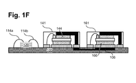
- Figure 1F illustrates a cross sectional view of a conventional buck converter mounted on a printed circuit board.
- Figure 1F includes a substrate 105, which may comprise a printed circuit board (PCB).
- Driver IC 120, package 141, and package 161 are disposed on substrate 105.
- Package 141 may correspond to package 141 as illustrated in Figure 1D and Figure 1E .
- Package 161 may also have a similar composition, substituting sync transistor 160 for control transistor 140.
- Wirebonds 114a and 114b may connect to pads on substrate 105 and further routed to respective gate terminals of packages 141 and 161.
- Trace 106 in substrate 105 may connect the control source 144 of package 141 to the sync drain 166 of package 161.
- Figure 1F may implement the buck converter in diagram 100 of Figure 1A .
- substrate 105 is utilized to implement the buck converter in diagram 100 of Figure 1A . More specifically, lateral space must be reserved for driver IC, package 141, package 161, vertical space must be reserved for wirebonds 114a and 114b, and various interconnects must be provided within substrate 105, such as trace 106. As a result, implementing the buck converter of Figure 1A using the conventional design of Figure 1F undesirably increases form factor, complexity, and cost.
- Figure 2A illustrates a top view of a high power semiconductor package according to an embodiment of the invention.
- Figure 2A includes package 210, which may comprise a QFN or another leadless package and includes driver 1C 220 disposed on pad 212a, control transistor 240 disposed on pad 212b, and sync transistor 260 disposed on pads 212a and 212d.
- Pad 212c is not connected in Figure 2A .
- Pads 212a through 212d may comprise pads of a substrate, such as, but not limited to, a printed circuit board (PCB), a ceramic substrate, direct bonded copper (DBC), or a leadframe.
- PCB printed circuit board
- DDC direct bonded copper
- control transistor 240 is oriented such that a control gate 242 and a control source 244 are disposed on a top surface thereof, with a control drain 246 (not shown) disposed on a bottom surface thereof.
- sync transistor 260 is oriented such that a sync gate 262 (not shown) and a sync source 264 (not shown) are disposed on a bottom surface thereof, with a sync drain 266 disposed on a top surface thereof.
- Wirebond 214a couples control gate 242 to driver IC 220
- wirebond 212b couples sync gate 262 to driver IC 220 through pad 212d.
- control transistor 240 and sync transistor 260 can be depletion mode transistors, for example, III-nitride depletion mode transistors.
- two transistors are utilized in package 210 of Figure 2A , alternative embodiments may also utilize more than two transistors.
- Figure 2B illustrates a top view of a high power semiconductor package with a multi-transistor conductive clip according to an embodiment of the invention.
- Figure 2B adds a conductive clip 280 to package 210 of Figure 2A .
- Conductive clip 280 may comprise any highly conductive material, including a metal such as copper or a metallic alloy, and is coupled to pad 212c, sync drain 266, and control source 244, for example by solder, conductive adhesive, or another attach material. Accordingly, conductive clip 280 electrically couples control source 244 to sync drain 266, corresponding to node 115 in Figure 1A .
- the layout of package 210 in Figure 2B connects driver IC 220, control transistor 240, and sync transistor 260 as shown in diagram 100 of Figure 1A .
- Figure 2C illustrates a top view of a high power semiconductor package with a multi-transistor exposed conductive clip according to an embodiment of the invention.
- a mold compound 213 is formed over control transistor 240 and sync transistor 260 without covering a top surface of conductive clip 280 from Figure 2B so as to form an exposed conductive clip 280 in Figure 2C .
- the top surface of package 210 may be abutted against an inner wall of a top pocket of a mold used to shape mold compound 213.
- conductive clip 280 may comprise a plurality of stacked clips rather than a single clip, allowing package 210 to extend higher while still exposing conductive clip 280, for example to provide sufficient clearance for wirebonds 214a and 214b.
- driver IC 220 may comprise a flip chip rather than a wirebonded IC, in which case driver IC 220 may also be exposed through mold compound 213 in a similar manner as exposed conductive clip 280, thereby providing enhanced thermal performance.
- a heat sink may be affixed to an exposed portion of exposed conductive clip 280 and/or driver IC 220.
- Figure 2D illustrates a cross sectional view of a high power semiconductor package according to an embodiment of the invention.
- the cross section shown in Figure 2D may correspond to the cross sectional line indicated by line 2D-2D of Figure 2C .
- package 210 includes pad 212d and 212a.
- a bottom surface of sync transistor 260 includes sync gate 262 disposed on pad 212d and sync source 264 disposed on pad 212a.
- a top surface of sync transistor 260 includes sync drain 266, which is coupled to exposed conductive clip 280.
- Package 210 is encapsulated within mold compound 213, which does not cover the top surface of exposed conductive clip 280.
- Figure 2E illustrates a cross sectional view of a high power semiconductor package according to an embodiment of the invention.
- the cross section shown in Figure 2E may correspond to the cross sectional line indicated by line 2E-2E of Figure 2C .
- package 210 includes pads 212c, 212a, and 212b.
- a bottom surface of sync transistor 260 includes sync source 264 disposed on pad 212a.
- a top surface of sync transistor 260 includes sync drain 266, which is coupled to exposed conductive clip 280.
- a bottom surface of control transistor 240 includes control drain 246 disposed on pad 212b.
- a top surface of control transistor 240 includes control source 244, which is coupled to exposed conductive clip 280.
- exposed conductive clip 280 electrically and mechanically couples pad 212c, sync drain 266, and control source 244.
- exposed conductive clip 280 provides an efficient current path between sync transistor 260 and control transistor 240 while providing enhanced thermal performance and reduced package form factor.
- Figure 2F illustrates a cross sectional view of a buck converter mounted on a printed circuit board according to an embodiment of the invention. Since package 210 as illustrated in Figures 2C, 2D, and 2E already implements the buck converter of diagram 100 in Figure 1A , no additional components are required. Thus, package 210 is simply mounted to support surface 205, such as printed circuit board.
- the reduced package form factor provided by package 210 is especially evident when comparing to the conventional design shown in Figure 1F , where driver IC 120, package 141, and package 161 are separately mounted to substrate 105.
- the efficient design of exposed conductive clip 280 where multiple transistors are coupled together and thermally exposed in a single package, provides package 210 with enhanced thermal and electrical performance suitable for high power applications.
- a multi-transistor exposed conductive clip for a high power semiconductor package has been described.
- an exposed conductive clip 280 that is coupled to multiple transistors to implement a desired circuit, such as a buck converter, a thermally and electrically enhanced semiconductor package may be provided for high power applications while optimizing package form factor compared to conventional packages.
Landscapes
- Dc-Dc Converters (AREA)
Abstract
One exemplary disclosed embodiment comprises a semiconductor package including multiple transistors (240,260) coupled to an exposed conductive clip (280). A driver integrated circuit (220) may control the transistors to implement a buck converter. By exposing a top surface of the exposed conductive clip outside of a mold compound (213) of the package, enhanced thermal performance is provided. Additionally, the conductive clip provides a short distance, high current carrying route between transistors of the package, providing higher electrical performance and reduced form factor compared to conventional designs with individually packaged transistors.
Description
- The present invention relates generally to semiconductor devices. More particularly, the present invention relates to packaging of semiconductor devices.
- Optimization of electrical and thermal performance is an important consideration for high frequency, high voltage power applications. It is known to use a conductive clip to provide a high performance interconnect between a transistor and input / output terminals within a package. Additionally, by exposing the conductive clip to the outside of the package, enhanced thermal dissipation may be provided, for example by affixing a heat sink to the exposed area of the conductive clip.
- In high power circuit applications, such as half-bridge based DC-DC converters or buck converters, multiple transistors are required. Additionally, a driver integrated circuit (IC) (or a "gate driver") is necessary to drive and control the transistors.
- Conventionally, the driver IC and the transistors may be individually packaged and disposed on a shared support surface, such as a printed circuit board (PCB). However, the routing of current lines through the PCB negatively affects electrical performance, and the form factor of the individual packages requires significant area to be reserved on the PCB, adding cost and complexity.
- Thus, a unique and cost-effective solution is needed to support the efficient design and operation of high power circuit applications, such as buck converters, while providing enhanced thermal dissipation and a compact form factor.
- A multi-transistor exposed conductive clip for high power semiconductor packages, substantially as shown in and/or described in connection with at least one of the figures, and as set forth more completely in the claims.
-
-
Figure 1A illustrates a circuit diagram of a buck converter using a half-bridge topology. -
Figure 1B illustrates a top view of a conventional semiconductor package. -
Figure 1C illustrates a top view of a conventional semiconductor package with a conductive clip. -
Figure 1D illustrates a top view of a conventional semiconductor package with an exposed conductive clip. -
Figure 1E illustrates a cross sectional view of a conventional semiconductor package with an exposed conductive clip. -
Figure 1F illustrates a cross sectional view of a conventional buck converter mounted on a printed circuit board. -
Figure 2A illustrates a top view of a high power semiconductor package according to an embodiment of the invention. -
Figure 2B illustrates a top view of a high power semiconductor package with a multi-transistor conductive clip according to an embodiment of the invention. -
Figure 2C illustrates a top view of a high power semiconductor package with a multi-transistor exposed conductive clip according to an embodiment of the invention. -
Figure 2D illustrates a cross sectional view of a high power semiconductor package according to an embodiment of the invention. -
Figure 2E illustrates a cross sectional view of a high power semiconductor package according to an embodiment of the invention. -
Figure 2F illustrates a cross sectional view of a buck converter mounted on a printed circuit board according to an embodiment of the invention. - The present application is directed to a multi-transistor exposed conductive clip for high power semiconductor packages. The following description contains specific information pertaining to the implementation of the present invention. One skilled in the art will recognize that the present invention may be implemented in a manner different from that specifically discussed in the present application. Moreover, some of the specific details of the invention are not discussed in order not to obscure the invention. The specific details not described in the present application are within the knowledge of a person of ordinary skill in the art.
- The drawings in the present application and their accompanying detailed description are directed to merely exemplary embodiments of the invention. To maintain brevity, other embodiments of the invention, which use the principles of the present invention, are not specifically described in the present application and are not specifically illustrated by the present drawings.
-
Figure 1A illustrates a circuit diagram of a buck converter using a half-bridge topology. Diagram 100 includes switchednode 115, driver integrated circuit (IC) 120, control transistor 140 (also referred to as a "control switch" or a "control FET"), and synchronous transistor 160 (also referred to as a "synchronous switch," a "sync switch," a "synchronous FET," or a "sync FET"). The source ofcontrol transistor 140 is coupled to the drain ofsync transistor 160 at switchednode 115.Driver IC 120 operates on voltage Vdr and controls the duty cycles ofcontrol transistor 140 andsync transistor 160, thereby converting the input voltage Vin to a specific output voltage Vout.Control transistor 140 andsync transistor 160 may each comprise a conventional field effect transistor (FET) switch, for example a silicon FET. However,control transistor 140 andsync transistor 160 may each also comprise a non-silicon FET or any other FET in general. Alternatively, one or both ofcontrol transistor 140 andsync transistor 160 may also comprise a III-nitride transistor. - To implement the buck converter of diagram 100 in
Figure 1A , it is known to packagedriver IC 120,control transistor 140, andsync transistor 160 into separate packages and connect them on a support surface such as a printed circuit board (PCB). Turning toFigure 1B, Figure 1B illustrates a top view of a conventional semiconductor package.Figure 1B includespackage 141, which may comprise, for example, a quad flat no-leads (QFN) package.Package 141 includespads wirebond 114a, andcontrol transistor 140.Pads Control transistor 140, which may correspond tocontrol transistor 140 fromFigure 1A , is disposed onpad 112a and includes a top surface having acontrol gate 142 and acontrol source 144 and a bottom surface (not shown) having acontrol drain 146.Control gate 142 is coupled topad 112b throughwirebond 114a. A similar package 161 (not shown) may also be fabricated by substitutingsync transistor 160 forcontrol transistor 140. - Moving to
Figure 1C, Figure 1C illustrates a top view of a conventional semiconductor package with a conductive clip.Figure 1C includespackage 141. ComparingFigure 1C withFigure 1B, Figure 1C adds aconductive clip 180 topackage 141 ofFigure 1B .Conductive clip 180 is coupled topad 112c andcontrol source 144. - Turning to
Figure 1D, Figure 1D illustrates a top view of a conventional semiconductor package with an exposed conductive clip.Figure 1D includespackage 141. ComparingFigure 1D withFigure 1C, Figure 1D adds an encapsulatingmold compound 113 topackage 141 ofFigure 1C . As shown inFigure 1D , themold compound 113 is formed such that a top surface ofconductive clip 180 is exposed, thereby resulting in an exposedconductive clip 180. For example, the top surface ofpackage 141 may be abutted against an inner wall of a top pocket of a mold used to shapemold compound 113. Exposedconductive clip 180 may provide enhanced thermal dissipation by radiating heat directly to ambient air or to an attached heat sink. The thermal performance ofpackage 141 may comprise an important long-term reliability consideration, particularly for high power applications. -
Figure 1E illustrates a cross sectional view of a conventional semiconductor package with an exposed conductive clip. The cross section shown inFigure 1E may correspond to the cross sectional line indicated byline 1E-1E ofFigure 1D. Figure 1E includespackage 141, which includespads control transistor 140 disposed onpad 112a and having a bottom surface including acontrol drain 146 and a top surface including acontrol gate 142 and acontrol source 144, awirebond 114acoupling control gate 142 to pad 112b, and an exposedconductive clip 180 coupled to controlsource 144 andpad 112c. - Addressing
Figure 1F, Figure 1F illustrates a cross sectional view of a conventional buck converter mounted on a printed circuit board.Figure 1F includes asubstrate 105, which may comprise a printed circuit board (PCB).Driver IC 120,package 141, andpackage 161 are disposed onsubstrate 105.Package 141 may correspond to package 141 as illustrated inFigure 1D and Figure 1E .Package 161 may also have a similar composition, substitutingsync transistor 160 forcontrol transistor 140.Wirebonds substrate 105 and further routed to respective gate terminals ofpackages Trace 106 insubstrate 105 may connect thecontrol source 144 ofpackage 141 to thesync drain 166 ofpackage 161. Thus,Figure 1F may implement the buck converter in diagram 100 ofFigure 1A . - However, a significant portion of
substrate 105 is utilized to implement the buck converter in diagram 100 ofFigure 1A . More specifically, lateral space must be reserved for driver IC,package 141,package 161, vertical space must be reserved for wirebonds 114a and 114b, and various interconnects must be provided withinsubstrate 105, such astrace 106. As a result, implementing the buck converter ofFigure 1A using the conventional design ofFigure 1F undesirably increases form factor, complexity, and cost. - Turning to
Figure 2A, Figure 2A illustrates a top view of a high power semiconductor package according to an embodiment of the invention.Figure 2A includespackage 210, which may comprise a QFN or another leadless package and includesdriver 1C 220 disposed onpad 212a,control transistor 240 disposed onpad 212b, andsync transistor 260 disposed onpads Pad 212c is not connected inFigure 2A .Pads 212a through 212d may comprise pads of a substrate, such as, but not limited to, a printed circuit board (PCB), a ceramic substrate, direct bonded copper (DBC), or a leadframe. As shown inFigure 2A ,control transistor 240 is oriented such that acontrol gate 242 and acontrol source 244 are disposed on a top surface thereof, with a control drain 246 (not shown) disposed on a bottom surface thereof. Conversely,sync transistor 260 is oriented such that a sync gate 262 (not shown) and a sync source 264 (not shown) are disposed on a bottom surface thereof, with async drain 266 disposed on a top surface thereof.Wirebond 214a couples controlgate 242 todriver IC 220, andwirebond 212b couplessync gate 262 todriver IC 220 throughpad 212d. - While
package 210 inFigure 2A is shown with continuous pad perimeters for simplicity, in alternative embodiments the perimeters ofpackage 210 may be separated into distinct pads. For example,pad 212a may comprise several individual pads to accommodate additional wirebond inputs and outputs fordriver IC 220.Pad control transistor 240 andsync transistor 260 can be depletion mode transistors, for example, III-nitride depletion mode transistors. Furthermore, while two transistors are utilized inpackage 210 ofFigure 2A , alternative embodiments may also utilize more than two transistors. - Turning to
Figure 2B, Figure 2B illustrates a top view of a high power semiconductor package with a multi-transistor conductive clip according to an embodiment of the invention. ComparingFigure 2B withFigure 2A, Figure 2B adds aconductive clip 280 to package 210 ofFigure 2A .Conductive clip 280 may comprise any highly conductive material, including a metal such as copper or a metallic alloy, and is coupled topad 212c,sync drain 266, and controlsource 244, for example by solder, conductive adhesive, or another attach material. Accordingly,conductive clip 280 electrically couples controlsource 244 to syncdrain 266, corresponding tonode 115 inFigure 1A . Thus, the layout ofpackage 210 inFigure 2B connectsdriver IC 220,control transistor 240, andsync transistor 260 as shown in diagram 100 ofFigure 1A . - With respect to
Figure 2C, Figure 2C illustrates a top view of a high power semiconductor package with a multi-transistor exposed conductive clip according to an embodiment of the invention. ComparingFigure 2C withFigure 2B , amold compound 213 is formed overcontrol transistor 240 andsync transistor 260 without covering a top surface ofconductive clip 280 fromFigure 2B so as to form an exposedconductive clip 280 inFigure 2C . For example, the top surface ofpackage 210 may be abutted against an inner wall of a top pocket of a mold used to shapemold compound 213. - In alternative embodiments,
conductive clip 280 may comprise a plurality of stacked clips rather than a single clip, allowingpackage 210 to extend higher while still exposingconductive clip 280, for example to provide sufficient clearance for wirebonds 214a and 214b. Alternatively,driver IC 220 may comprise a flip chip rather than a wirebonded IC, in whichcase driver IC 220 may also be exposed throughmold compound 213 in a similar manner as exposedconductive clip 280, thereby providing enhanced thermal performance. Optionally, a heat sink may be affixed to an exposed portion of exposedconductive clip 280 and/ordriver IC 220. - Moving to
Figure 2D, Figure 2D illustrates a cross sectional view of a high power semiconductor package according to an embodiment of the invention. The cross section shown inFigure 2D may correspond to the cross sectional line indicated byline 2D-2D ofFigure 2C . As shown inFigure 2D ,package 210 includespad sync transistor 260 includessync gate 262 disposed onpad 212d andsync source 264 disposed onpad 212a. A top surface ofsync transistor 260 includessync drain 266, which is coupled to exposedconductive clip 280.Package 210 is encapsulated withinmold compound 213, which does not cover the top surface of exposedconductive clip 280. - Discussing
Figure 2E, Figure 2E illustrates a cross sectional view of a high power semiconductor package according to an embodiment of the invention. The cross section shown inFigure 2E may correspond to the cross sectional line indicated byline 2E-2E ofFigure 2C . As shown inFigure 2E ,package 210 includespads sync transistor 260 includessync source 264 disposed onpad 212a. A top surface ofsync transistor 260 includessync drain 266, which is coupled to exposedconductive clip 280. A bottom surface ofcontrol transistor 240 includescontrol drain 246 disposed onpad 212b. A top surface ofcontrol transistor 240 includescontrol source 244, which is coupled to exposedconductive clip 280. Thus, exposedconductive clip 280 electrically and mechanically couplespad 212c,sync drain 266, and controlsource 244. Bycoupling sync drain 266 and controlsource 244 through a low resistance, short distance path while also being exposed to the outside ofpackage 210, exposedconductive clip 280 provides an efficient current path betweensync transistor 260 andcontrol transistor 240 while providing enhanced thermal performance and reduced package form factor. - The advantages of the reduced package form factor provided by
package 210 are further emphasized inFigure 2F , which illustrates a cross sectional view of a buck converter mounted on a printed circuit board according to an embodiment of the invention. Sincepackage 210 as illustrated inFigures 2C, 2D, and 2E already implements the buck converter of diagram 100 inFigure 1A , no additional components are required. Thus,package 210 is simply mounted to supportsurface 205, such as printed circuit board. The reduced package form factor provided bypackage 210 is especially evident when comparing to the conventional design shown inFigure 1F , wheredriver IC 120,package 141, andpackage 161 are separately mounted tosubstrate 105. The efficient design of exposedconductive clip 280, where multiple transistors are coupled together and thermally exposed in a single package, providespackage 210 with enhanced thermal and electrical performance suitable for high power applications. - Thus, a multi-transistor exposed conductive clip for a high power semiconductor package has been described. According to the present invention, by using an exposed
conductive clip 280 that is coupled to multiple transistors to implement a desired circuit, such as a buck converter, a thermally and electrically enhanced semiconductor package may be provided for high power applications while optimizing package form factor compared to conventional packages. - From the above description of the invention it is manifest that various techniques can be used for implementing the concepts of the present invention without departing from its scope. Moreover, while the invention has been described with specific reference to certain embodiments, a person of ordinary skills in the art would recognize that changes can be made in form and detail without departing from the spirit and the scope of the invention. As such, the described embodiments are to be considered in all respects as illustrative and not restrictive. It should also be understood that the invention is not limited to the particular embodiments described herein, but is capable of many rearrangements, modifications, and substitutions without departing from the scope of the invention.
Claims (15)
- A high power semiconductor package comprising:at least two transistors including a control transistor having a control source on a top surface thereof and a sync transistor having a sync drain on a top surface thereof;a driver integrated circuit (IC) driving said at least two transistors;an exposed conductive clip coupled to said control source and said sync drain;a mold compound enclosing said at least two transistors without covering a top surface of said exposed conductive clip.
- The high power semiconductor package of claim 1, wherein said driver IC is a flip chip.
- The high power semiconductor package of claim 1, wherein said package comprises a buck converter.
- The high power semiconductor package of claim 1, wherein said exposed conductive clip is coupled using solder.
- The high power semiconductor package of claim 1, wherein said exposed conductive clip is further attached to a leadframe pad of said package.
- The high power semiconductor package of claim 1, wherein said exposed conductive clip comprises a copper clip.
- The high power semiconductor package of claim 1, wherein said exposed conductive clip comprises a plurality of stacked clips.
- The high power semiconductor package of claim 1, wherein said package is a leadless package.
- The high power semiconductor package of claim 1, wherein said at least two transistors include a III-nitride depletion mode transistor.
- A high power semiconductor package comprising:a control transistor including a top surface having a control gate and a control source;a sync transistor including a top surface having a sync drain and a bottom surface including a sync gate;a driver integrated circuit (IC) coupled to said control gate and said sync gate;an exposed conductive clip coupled to said control source and said sync drain;a mold compound enclosing said control transistor and said sync transistor without covering a top surface of said exposed conductive clip.
- The high power semiconductor package of claim 10, wherein said driver IC is a flip chip.
- The high power semiconductor package of claim 10, wherein said package comprises a buck converter.
- The high power semiconductor package of claim 10, wherein said exposed conductive clip is further attached to a leadframe pad of said package.
- The high power semiconductor package of claim 10, wherein said control transistor is a III-nitride depletion mode transistor.
- The high power semiconductor package of claim 10, wherein said sync transistor is a III-nitride depletion mode transistor.
Applications Claiming Priority (1)
| Application Number | Priority Date | Filing Date | Title |
|---|---|---|---|
| US13/111,712 US8344464B2 (en) | 2011-05-19 | 2011-05-19 | Multi-transistor exposed conductive clip for high power semiconductor packages |
Publications (1)
| Publication Number | Publication Date |
|---|---|
| EP2525400A1 true EP2525400A1 (en) | 2012-11-21 |
Family
ID=46085391
Family Applications (1)
| Application Number | Title | Priority Date | Filing Date |
|---|---|---|---|
| EP12165277A Withdrawn EP2525400A1 (en) | 2011-05-19 | 2012-04-24 | High power semiconductor package including transistors interconnected through an exposed conductive clip |
Country Status (2)
| Country | Link |
|---|---|
| US (2) | US8344464B2 (en) |
| EP (1) | EP2525400A1 (en) |
Cited By (1)
| Publication number | Priority date | Publication date | Assignee | Title |
|---|---|---|---|---|
| EP3007227A1 (en) * | 2014-10-08 | 2016-04-13 | International Rectifier Corporation | Compact power semiconductor package |
Families Citing this family (24)
| Publication number | Priority date | Publication date | Assignee | Title |
|---|---|---|---|---|
| US8637909B1 (en) * | 2010-08-11 | 2014-01-28 | Sarda Technologies, Inc. | Mixed mode dual switch |
| US9236378B2 (en) | 2010-08-11 | 2016-01-12 | Sarda Technologies, Inc. | Integrated switch devices |
| US8896034B1 (en) | 2010-08-11 | 2014-11-25 | Sarda Technologies, Inc. | Radio frequency and microwave devices and methods of use |
| TWI453831B (en) | 2010-09-09 | 2014-09-21 | 台灣捷康綜合有限公司 | Semiconductor package and method for making the same |
| US8896107B2 (en) * | 2011-01-03 | 2014-11-25 | International Rectifier Corporation | High power semiconductor package with conductive clip |
| US8344464B2 (en) | 2011-05-19 | 2013-01-01 | International Rectifier Corporation | Multi-transistor exposed conductive clip for high power semiconductor packages |
| US9111776B2 (en) * | 2012-10-18 | 2015-08-18 | International Rectifier Corporation | Power semiconductor package with non-contiguous, multi-section conductive carrier |
| US9111921B2 (en) | 2012-10-18 | 2015-08-18 | International Rectifier Corporation | Semiconductor package with conductive carrier integrated heat spreader |
| US9054040B2 (en) | 2013-02-27 | 2015-06-09 | Infineon Technologies Austria Ag | Multi-die package with separate inter-die interconnects |
| US9589929B2 (en) | 2013-03-14 | 2017-03-07 | Vishay-Siliconix | Method for fabricating stack die package |
| US9966330B2 (en) * | 2013-03-14 | 2018-05-08 | Vishay-Siliconix | Stack die package |
| US9041170B2 (en) | 2013-04-02 | 2015-05-26 | Infineon Technologies Austria Ag | Multi-level semiconductor package |
| US9177925B2 (en) | 2013-04-18 | 2015-11-03 | Fairfchild Semiconductor Corporation | Apparatus related to an improved package including a semiconductor die |
| US9536800B2 (en) | 2013-12-07 | 2017-01-03 | Fairchild Semiconductor Corporation | Packaged semiconductor devices and methods of manufacturing |
| US9653386B2 (en) * | 2014-10-16 | 2017-05-16 | Infineon Technologies Americas Corp. | Compact multi-die power semiconductor package |
| US9620475B2 (en) | 2013-12-09 | 2017-04-11 | Infineon Technologies Americas Corp | Array based fabrication of power semiconductor package with integrated heat spreader |
| US9704787B2 (en) | 2014-10-16 | 2017-07-11 | Infineon Technologies Americas Corp. | Compact single-die power semiconductor package |
| US9570379B2 (en) | 2013-12-09 | 2017-02-14 | Infineon Technologies Americas Corp. | Power semiconductor package with integrated heat spreader and partially etched conductive carrier |
| US9735112B2 (en) | 2014-01-10 | 2017-08-15 | Fairchild Semiconductor Corporation | Isolation between semiconductor components |
| DE102015104995B4 (en) | 2015-03-31 | 2020-06-04 | Infineon Technologies Austria Ag | Compound semiconductor device with a multi-stage carrier |
| US9768130B2 (en) * | 2015-10-26 | 2017-09-19 | Texas Instruments Incorporated | Integrated power package |
| US9774322B1 (en) | 2016-06-22 | 2017-09-26 | Sarda Technologies, Inc. | Gate driver for depletion-mode transistors |
| US10128170B2 (en) | 2017-01-09 | 2018-11-13 | Silanna Asia Pte Ltd | Conductive clip connection arrangements for semiconductor packages |
| US10930604B2 (en) | 2018-03-29 | 2021-02-23 | Semiconductor Components Industries, Llc | Ultra-thin multichip power devices |
Citations (3)
| Publication number | Priority date | Publication date | Assignee | Title |
|---|---|---|---|---|
| US20050161785A1 (en) * | 2004-01-28 | 2005-07-28 | Tetsuya Kawashima | Semiconductor device |
| US20070249092A1 (en) * | 2006-04-24 | 2007-10-25 | Rajeev Joshi | Semiconductor die package including multiple dies and a common node structure |
| US20110080156A1 (en) * | 2006-11-28 | 2011-04-07 | International Rectifier Corporation | DC/DC converter with depletion-mode III-nitride switches |
Family Cites Families (12)
| Publication number | Priority date | Publication date | Assignee | Title |
|---|---|---|---|---|
| US6566164B1 (en) | 2000-12-07 | 2003-05-20 | Amkor Technology, Inc. | Exposed copper strap in a semiconductor package |
| US6946740B2 (en) | 2002-07-15 | 2005-09-20 | International Rectifier Corporation | High power MCM package |
| JP2008545274A (en) | 2005-06-30 | 2008-12-11 | フェアチャイルド セミコンダクター コーポレイション | Semiconductor die package and manufacturing method thereof |
| JP4916745B2 (en) * | 2006-03-28 | 2012-04-18 | ルネサスエレクトロニクス株式会社 | Manufacturing method of semiconductor device |
| US7663211B2 (en) | 2006-05-19 | 2010-02-16 | Fairchild Semiconductor Corporation | Dual side cooling integrated power device package and module with a clip attached to a leadframe in the package and the module and methods of manufacture |
| US7898093B1 (en) | 2006-11-02 | 2011-03-01 | Amkor Technology, Inc. | Exposed die overmolded flip chip package and fabrication method |
| TW200835126A (en) | 2006-11-28 | 2008-08-16 | Int Rectifier Corp | Synchronous DC/DC converter |
| KR101469770B1 (en) * | 2007-11-21 | 2014-12-09 | 페어차일드코리아반도체 주식회사 | Power device package and manufacturing method thereof |
| US7994615B2 (en) * | 2009-08-28 | 2011-08-09 | International Rectifier Corporation | Direct contact leadless package for high current devices |
| US8896107B2 (en) * | 2011-01-03 | 2014-11-25 | International Rectifier Corporation | High power semiconductor package with conductive clip |
| US8680627B2 (en) * | 2011-01-14 | 2014-03-25 | International Rectifier Corporation | Stacked half-bridge package with a common conductive clip |
| US8344464B2 (en) | 2011-05-19 | 2013-01-01 | International Rectifier Corporation | Multi-transistor exposed conductive clip for high power semiconductor packages |
-
2011
- 2011-05-19 US US13/111,712 patent/US8344464B2/en active Active
-
2012
- 2012-04-24 EP EP12165277A patent/EP2525400A1/en not_active Withdrawn
- 2012-12-27 US US13/727,899 patent/US9281306B2/en active Active
Patent Citations (3)
| Publication number | Priority date | Publication date | Assignee | Title |
|---|---|---|---|---|
| US20050161785A1 (en) * | 2004-01-28 | 2005-07-28 | Tetsuya Kawashima | Semiconductor device |
| US20070249092A1 (en) * | 2006-04-24 | 2007-10-25 | Rajeev Joshi | Semiconductor die package including multiple dies and a common node structure |
| US20110080156A1 (en) * | 2006-11-28 | 2011-04-07 | International Rectifier Corporation | DC/DC converter with depletion-mode III-nitride switches |
Cited By (3)
| Publication number | Priority date | Publication date | Assignee | Title |
|---|---|---|---|---|
| EP3007227A1 (en) * | 2014-10-08 | 2016-04-13 | International Rectifier Corporation | Compact power semiconductor package |
| US9768087B2 (en) | 2014-10-08 | 2017-09-19 | Infineon Technologies Americas Corp. | Compact high-voltage semiconductor package |
| US10083884B2 (en) | 2014-10-08 | 2018-09-25 | Infineon Technologies Americas Corp. | Compact high-voltage semiconductor package |
Also Published As
| Publication number | Publication date |
|---|---|
| US8344464B2 (en) | 2013-01-01 |
| US9281306B2 (en) | 2016-03-08 |
| US20120292753A1 (en) | 2012-11-22 |
| US20130134524A1 (en) | 2013-05-30 |
Similar Documents
| Publication | Publication Date | Title |
|---|---|---|
| US8344464B2 (en) | Multi-transistor exposed conductive clip for high power semiconductor packages | |
| US8531016B2 (en) | Thermally enhanced semiconductor package with exposed parallel conductive clip | |
| KR101168973B1 (en) | Semiconductor device | |
| US8749034B2 (en) | High power semiconductor package with conductive clip and flip chip driver IC with integrated control transistor | |
| US8614503B2 (en) | Common drain exposed conductive clip for high power semiconductor packages | |
| JP4250191B2 (en) | Semiconductor device for DC / DC converter | |
| US8860194B2 (en) | Buck converter power package | |
| JP4705945B2 (en) | Semiconductor device | |
| JP2011181970A (en) | Semiconductor device | |
| JP4250193B2 (en) | Semiconductor device for DC / DC converter | |
| JP4800290B2 (en) | Semiconductor device |
Legal Events
| Date | Code | Title | Description |
|---|---|---|---|
| PUAI | Public reference made under article 153(3) epc to a published international application that has entered the european phase |
Free format text: ORIGINAL CODE: 0009012 |
|
| AK | Designated contracting states |
Kind code of ref document: A1 Designated state(s): AL AT BE BG CH CY CZ DE DK EE ES FI FR GB GR HR HU IE IS IT LI LT LU LV MC MK MT NL NO PL PT RO RS SE SI SK SM TR |
|
| AX | Request for extension of the european patent |
Extension state: BA ME |
|
| 17P | Request for examination filed |
Effective date: 20130517 |
|
| 17Q | First examination report despatched |
Effective date: 20171120 |
|
| STAA | Information on the status of an ep patent application or granted ep patent |
Free format text: STATUS: THE APPLICATION HAS BEEN WITHDRAWN |
|
| 18W | Application withdrawn |
Effective date: 20180228 |