EP2523328A2 - Electronic device - Google Patents
Electronic device Download PDFInfo
- Publication number
- EP2523328A2 EP2523328A2 EP12167407A EP12167407A EP2523328A2 EP 2523328 A2 EP2523328 A2 EP 2523328A2 EP 12167407 A EP12167407 A EP 12167407A EP 12167407 A EP12167407 A EP 12167407A EP 2523328 A2 EP2523328 A2 EP 2523328A2
- Authority
- EP
- European Patent Office
- Prior art keywords
- voltage
- terminal
- feedback coil
- transformer
- value
- Prior art date
- Legal status (The legal status is an assumption and is not a legal conclusion. Google has not performed a legal analysis and makes no representation as to the accuracy of the status listed.)
- Withdrawn
Links
- 230000003247 decreasing effect Effects 0.000 claims abstract description 6
- 230000007423 decrease Effects 0.000 claims abstract description 4
- 101100100146 Candida albicans NTC1 gene Proteins 0.000 description 5
- 238000010586 diagram Methods 0.000 description 2
- 238000009499 grossing Methods 0.000 description 2
- 239000004973 liquid crystal related substance Substances 0.000 description 2
- XEEYBQQBJWHFJM-UHFFFAOYSA-N Iron Chemical group [Fe] XEEYBQQBJWHFJM-UHFFFAOYSA-N 0.000 description 1
- 230000002159 abnormal effect Effects 0.000 description 1
- 238000006243 chemical reaction Methods 0.000 description 1
- 238000012544 monitoring process Methods 0.000 description 1
- 238000013021 overheating Methods 0.000 description 1
- 238000006467 substitution reaction Methods 0.000 description 1
- 238000002834 transmittance Methods 0.000 description 1
Images

Classifications
-
- H—ELECTRICITY
- H02—GENERATION; CONVERSION OR DISTRIBUTION OF ELECTRIC POWER
- H02M—APPARATUS FOR CONVERSION BETWEEN AC AND AC, BETWEEN AC AND DC, OR BETWEEN DC AND DC, AND FOR USE WITH MAINS OR SIMILAR POWER SUPPLY SYSTEMS; CONVERSION OF DC OR AC INPUT POWER INTO SURGE OUTPUT POWER; CONTROL OR REGULATION THEREOF
- H02M3/00—Conversion of DC power input into DC power output
- H02M3/22—Conversion of DC power input into DC power output with intermediate conversion into AC
- H02M3/24—Conversion of DC power input into DC power output with intermediate conversion into AC by static converters
- H02M3/28—Conversion of DC power input into DC power output with intermediate conversion into AC by static converters using discharge tubes with control electrode or semiconductor devices with control electrode to produce the intermediate AC
- H02M3/325—Conversion of DC power input into DC power output with intermediate conversion into AC by static converters using discharge tubes with control electrode or semiconductor devices with control electrode to produce the intermediate AC using devices of a triode or a transistor type requiring continuous application of a control signal
- H02M3/335—Conversion of DC power input into DC power output with intermediate conversion into AC by static converters using discharge tubes with control electrode or semiconductor devices with control electrode to produce the intermediate AC using devices of a triode or a transistor type requiring continuous application of a control signal using semiconductor devices only
- H02M3/33507—Conversion of DC power input into DC power output with intermediate conversion into AC by static converters using discharge tubes with control electrode or semiconductor devices with control electrode to produce the intermediate AC using devices of a triode or a transistor type requiring continuous application of a control signal using semiconductor devices only with automatic control of the output voltage or current, e.g. flyback converters
- H02M3/33523—Conversion of DC power input into DC power output with intermediate conversion into AC by static converters using discharge tubes with control electrode or semiconductor devices with control electrode to produce the intermediate AC using devices of a triode or a transistor type requiring continuous application of a control signal using semiconductor devices only with automatic control of the output voltage or current, e.g. flyback converters with galvanic isolation between input and output of both the power stage and the feedback loop
-
- H—ELECTRICITY
- H02—GENERATION; CONVERSION OR DISTRIBUTION OF ELECTRIC POWER
- H02M—APPARATUS FOR CONVERSION BETWEEN AC AND AC, BETWEEN AC AND DC, OR BETWEEN DC AND DC, AND FOR USE WITH MAINS OR SIMILAR POWER SUPPLY SYSTEMS; CONVERSION OF DC OR AC INPUT POWER INTO SURGE OUTPUT POWER; CONTROL OR REGULATION THEREOF
- H02M1/00—Details of apparatus for conversion
- H02M1/32—Means for protecting converters other than automatic disconnection
Definitions
- the present invention relates to an electronic device having a power circuit to generate a power by driving a switching element.
- an electronic device includes a power circuit.
- power is generated at the power circuit and supplied to a circuit connected to a secondary coil of a transformer.
- the electronic device includes a switching element and an IC (Integrated Circuit) for driving the switching element.
- the power circuit generates a predetermined power under the control of the IC.
- a power circuit is disclosed in the following documents:
- IC for the power circuit can have a function to detect a voltage value generated at a feedback coil and adjust a timing to output a drive signal according to the detected voltage value.
- the 1C detects a timing when a signal generated at the feedback coil becomes 0V and outputs the drive signal to the switching element in order to synchronize with the detected timing.
- the IC may output the signal having an abnormal waveform.
- the present invention provides a power circuit to stop the circuit safely even when the feedback coil is broken.
- One aspect of the present invention provides an electronic device having an electronic circuit, comprising:
- the IC is a part of the electric circuit and the IC has the voltage decreasing portion that decreases the voltage applied at the second terminal when the voltage supplied by the feedback coil is equal to or lower than the predetermined value. Therefore, the voltage decreasing portion reduces the voltage applied at the second terminal of the IC when the feedback coil is damaged and the voltage supplied by the feedback coil is equal to or lower than the predetermined value. Consequently, the voltage value applied at the second terminal of the IC becomes equal to or lower than the threshold value and then the IC is latched.
- the circuit can be stopped safely even when the feedback coil is broken.
- the display device 100 includes a liquid crystal display panel 99, a main controller 98, a driver 97, and a power circuit 80.
- images are displayed on the display panel 99 based on image data input from an external device (not illustrated) or broadcasting signal received through a tuner (not illustrated).
- the display panel 99 includes a screen on which picture elements are aligned according to a resolution of the display panel 99, and liquid crystal is filled in each picture element.
- the screen is composed of picture elements and electrodes are provided to each sides of the picture element. By supplying a drive voltage to the electrode, the picture element is driven and light transmittance of the picture element can be changed.
- the display panel 99 also includes many switches to select scanning lines to drive the picture elements. The drive voltage is supplied to the electrodes on the scanning lines selected by the switches.
- the main controller 98 includes a CPU (Central Processing Unit) to carry out an operation, a ROM (Read Only Memory) in which programs to enable the CPU to carry out the operation are recorded, and a RAM (Random Access Memory) that is used by the CPU as a working area. If image data or other data is received through a tuner (not illustrated) or the like, the main controller 98 carries out a predetermined signal processing and then outputs the received data to the driver 97.
- a CPU Central Processing Unit
- ROM Read Only Memory
- RAM Random Access Memory
- the driver 97 performs digital-to-analog conversion to the image data, and generates a drive voltage according to a gradation value indicated by the image data.
- the driver 97 supplies the drive voltage to the electrodes on the scanning lines of the display panel based on a vertical synchronizing signal and a horizontal synchronizing signal included in the image data. Therefore, the electrodes drive the picture elements corresponding to the electrodes by adding the drive voltage to the picture elements.
- Fig. 2 shows a partial structure of a power circuit 80.
- Fig. 3 shows a structure of an IC 1.
- the power circuit 80 generates a power based on the power supplied from a commercial power supply (AC 100V, not illustrated) to drive a secondary circuit of the display device 100.
- the secondary circuit is the display panel 99, the main controller 98, and the driver 97 in the present embodiment.
- the power circuit 80 generates a predetermined voltage by switching a FET Q1 (switching element) and then supplies the predetermined voltage to the secondary circuit. Therefore, roughly speaking, the power circuit 80 includes an IC 1, the FET Q1, a transformer T1, and a feedback coil Cof.
- a HV terminal 14 of the IC 1 receives a DC voltage (VCC-ON) to drive the IC 1.
- VCC-ON is a voltage generated at a primary side (not illustrated) of the power circuit 80.
- a DRV terminal 9 of the IC 1 is connected to a gate of the FET Q1 through a drive circuit that is configured by a register R9 and a transistor Q2.
- a junction between a drain and a source of the FET Q1 is connected to one end of a primary coil Col of the transformer T1.
- Another end of the primary coil Co1 is supplied voltage through a rectifier circuit and a smoothing circuit that are not illustrated.
- the feedback coil Cof is aligned to face a secondary coil Co2 of the transformer T1 placing an iron core in the center, and is connected to a ZCD terminal 4 of the IC 1 through a diode D2 and registers R2, R3.
- a VCC-ON signal that indicates an operation to turn on a main power is input to the HV terminal 14 of the IC 1
- a pulse signal is output from an internal block 20 of the IC 1 thorough the DRV terminal 9.
- the pulse signal is output as a pulse drive signal to the FET Q1 through the drive circuit.
- the FET Q1 is turned on, and the voltage is supplied to the primary coil Co of the transformer T1 through the rectifier circuit and the smoothing circuit. Consequently, the predetermined voltage is generated at the secondary coil Co2 of the transformer T1.
- a feedback voltage Vf that has a sinusoidal wave is generated at the feedback coil Cof.
- the IC 1 monitors a change in a waveform of the feedback voltage Vf using the ZCD terminal 4 (first terminal).
- the IC 1 includes an internal block 21 that detects a timing when the feedback voltage Vf becomes 0V, and the IC 1 outputs the drive signal from the DRV terminal 9 at the timing when the feedback voltage Vf becomes 0V Therefore, the FET Q1 continues switching operation in the power circuit 80, and the predetermined voltage is supplied to the secondary circuit from the secondary coil Co2.
- the IC 1 is prevented from overheating by monitoring the voltage applied at an OTP (Over Temperature Protection) terminal 2 (second terminal).
- OTP Over Temperature Protection
- the OTP terminal 2 of the IC 1 is grounded through a thermister NTC1.
- the IC 1 includes an internal block 22 that applies current to the thermister NTC1 from the OTP terminal 2 and compares the voltage specified by the thermister NTC1 with a threshold value S in order to latch the IC 1 according to the comparison result.
- the threshold value S is specified to 1.0V in the internal block 22 of the IC 1 in the present embodiment. In an ordinary condition, voltage of 3.0V is applied at the OTP terminal 2.
- the internal block 22 latches the IC1 to stop outputting the drive signal. Consequently, the IC 1 stops driving the power circuit 80.
- the IC 1 monitors overvoltage of the secondary coil Co2 using an OVP (Over Voltage Protection) terminal 12 based on the feedback voltage Vf generated at the feedback coil Cof.
- OVP Over Voltage Protection
- one end of the feedback coil Cof is connected to the diode D2 and registers R2, R3 in series. Therefore, the feedback voltage Vf is generated at a contact point (OVP point) between the register R2 and the register R3 after rectified by the diode D2 and divided by the registers R2, R3.
- an anode of a Zener diode D3 that detects the overvoltage is connected to the OVP terminal 12 thorough a diode D11. Consequently, the IC 1 monitors a voltage value at the OVP point from the OVP terminal 12 using the Zener diode D3.
- the feedback voltage Vf may not be fed back correctly.
- the voltage generated at the transformer T1 may be unexpected value because the drive signal output from the IC 1 is kept at a high level or a duty ratio of the drive signal is changed to unexpected value.
- the present invention provides a solution to stop driving the power circuit 80 safely in case the feedback coil Cof is broken.
- the OTP terminal 2 of the IC 1 is connected to the feedback coil Cof through a diode D12 (voltage reducing portion). Specifically, the OTP terminal 2 is connected to an anode of the diode D12. In addition, a cathode of the diode D12 is connected to a point A to connect to the OVP point that detects a voltage value of the feedback coil Cof. Furthermore, the point A is connected to the ground thorough a condenser C2.
- the feedback coil Cof is normal, although the feedback voltage Vf changes within a range of 0V to 5V, a potential difference between both sides of the diode D12 does not appear continuously and a current does not flow through the diode D12. Therefore, the voltage supplied to the OTP terminal 2 varies only depending on the ohmic value of the thermister NTC1. If the feedback coil Cof is damaged and short-circuited, an electric potential at the point A is kept around 0V, the potential difference between both sides of the diode D12 appears continuously, and a current flows through the diode D12. Therefore, the voltage applied at the OTP terminal 2 drops down rapidly and the internal block 22 works to latch the IC 1 when the voltage is equal to or below the threshold value S (e.g. 1.0V). Consequently, the drive signal is not output from the DRV terminal 9 of the IC 1 and the FET Q1 stops switching operation to stop driving the power circuit 80.
- S e.g. 1.0V
- the power circuit 80 in the present embodiment can be safely stopped by latching IC 1 to stop supplying the drive signal.
Landscapes
- Engineering & Computer Science (AREA)
- Power Engineering (AREA)
- Dc-Dc Converters (AREA)
Abstract
Description
- The present invention relates to an electronic device having a power circuit to generate a power by driving a switching element.
- Conventionally, an electronic device includes a power circuit.
In the electronic device, power is generated at the power circuit and supplied to a circuit connected to a secondary coil of a transformer. In addition, the electronic device includes a switching element and an IC (Integrated Circuit) for driving the switching element. The power circuit generates a predetermined power under the control of the IC. For example, such a power circuit is disclosed in the following documents: - Japanese Patent Application Publication
2006-352975 - Japanese Patent Application Publication
2004-120926 - Japanese Patent Application Publication
2003-259636 - Japanese Patent Application Publication
H09-121537 - Japanese Patent Application Publication
2006-254590 - Above described IC for the power circuit can have a function to detect a voltage value generated at a feedback coil and adjust a timing to output a drive signal according to the detected voltage value. For example, the 1C detects a timing when a signal generated at the feedback coil becomes 0V and outputs the drive signal to the switching element in order to synchronize with the detected timing.
- In the power circuit that includes the above described IC, if the feedback coil is broken in some reason, the IC may output the signal having an abnormal waveform.
- The present invention provides a power circuit to stop the circuit safely even when the feedback coil is broken.
- One aspect of the present invention provides an electronic device having an electronic circuit, comprising:
- a transformer;
- a switching element that generates a predetermined voltage at the transformer by a switching operation;
- an IC that outputs a drive signal to drive the switching element, and a feedback coil that feeds back a voltage generated at a secondary coil of the transformer, wherein
- the IC monitors a voltage value of the feedback coil using a first terminal and outputs the drive signal to drive the switching element according to the voltage value of the feedback coil,
- the IC is latched when a voltage value applied at a second terminal is equal to or lower than a threshold value, and
- the IC has a voltage decreasing portion that decreases the voltage applied at the second terminal when the voltage supplied by the feedback coil is equal to or lower than a predetermined value.
- In the above structured invention, the IC is a part of the electric circuit and the IC has the voltage decreasing portion that decreases the voltage applied at the second terminal when the voltage supplied by the feedback coil is equal to or lower than the predetermined value. Therefore, the voltage decreasing portion reduces the voltage applied at the second terminal of the IC when the feedback coil is damaged and the voltage supplied by the feedback coil is equal to or lower than the predetermined value. Consequently, the voltage value applied at the second terminal of the IC becomes equal to or lower than the threshold value and then the IC is latched.
- Therefore, in the present invention, the circuit can be stopped safely even when the feedback coil is broken.
-
-
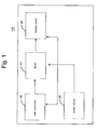
Fig. 1 is a block diagram showing a structure of an electronic device. -
Fig. 2 shows a partial structure of apower circuit 80. -
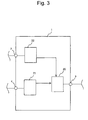
Fig. 3 shows a structure of anIC 1. - Hereinafter, embodiments of the present invention will be explained in the following order.
- 1. The first embodiment:
- 2. Other embodiments:
- 1. The first embodiment:
- The present invention concerning an electronic device will be explained below with reference to figures.
Fig. 1 is a block diagram showing a structure of an electronic device. Note that adisplay device 100 is used as an example of the electronic device in the following explanation. - As shown in
Fig. 1 , thedisplay device 100 includes a liquidcrystal display panel 99, amain controller 98, adriver 97, and apower circuit 80. In thedisplay device 100, images are displayed on thedisplay panel 99 based on image data input from an external device (not illustrated) or broadcasting signal received through a tuner (not illustrated). - The
display panel 99 includes a screen on which picture elements are aligned according to a resolution of thedisplay panel 99, and liquid crystal is filled in each picture element. The screen is composed of picture elements and electrodes are provided to each sides of the picture element. By supplying a drive voltage to the electrode, the picture element is driven and light transmittance of the picture element can be changed. Thedisplay panel 99 also includes many switches to select scanning lines to drive the picture elements. The drive voltage is supplied to the electrodes on the scanning lines selected by the switches. - The
main controller 98 includes a CPU (Central Processing Unit) to carry out an operation, a ROM (Read Only Memory) in which programs to enable the CPU to carry out the operation are recorded, and a RAM (Random Access Memory) that is used by the CPU as a working area. If image data or other data is received through a tuner (not illustrated) or the like, themain controller 98 carries out a predetermined signal processing and then outputs the received data to thedriver 97. - The
driver 97 performs digital-to-analog conversion to the image data, and generates a drive voltage according to a gradation value indicated by the image data. In addition, thedriver 97 supplies the drive voltage to the electrodes on the scanning lines of the display panel based on a vertical synchronizing signal and a horizontal synchronizing signal included in the image data. Therefore, the electrodes drive the picture elements corresponding to the electrodes by adding the drive voltage to the picture elements. -
Fig. 2 shows a partial structure of apower circuit 80.Fig. 3 shows a structure of anIC 1.
Thepower circuit 80 generates a power based on the power supplied from a commercial power supply (AC 100V, not illustrated) to drive a secondary circuit of thedisplay device 100. The secondary circuit is thedisplay panel 99, themain controller 98, and thedriver 97 in the present embodiment. In the present embodiment, thepower circuit 80 generates a predetermined voltage by switching a FET Q1 (switching element) and then supplies the predetermined voltage to the secondary circuit. Therefore, roughly speaking, thepower circuit 80 includes anIC 1, the FET Q1, a transformer T1, and a feedback coil Cof. - More specifically, a
HV terminal 14 of theIC 1 receives a DC voltage (VCC-ON) to drive theIC 1. Here, the VCC-ON is a voltage generated at a primary side (not illustrated) of thepower circuit 80. ADRV terminal 9 of theIC 1 is connected to a gate of the FET Q1 through a drive circuit that is configured by a register R9 and a transistor Q2. A junction between a drain and a source of the FET Q1 is connected to one end of a primary coil Col of the transformer T1. Another end of the primary coil Co1 is supplied voltage through a rectifier circuit and a smoothing circuit that are not illustrated. The feedback coil Cof is aligned to face a secondary coil Co2 of the transformer T1 placing an iron core in the center, and is connected to aZCD terminal 4 of theIC 1 through a diode D2 and registers R2, R3. - In the above described
power circuit 80, if a VCC-ON signal that indicates an operation to turn on a main power is input to theHV terminal 14 of theIC 1, a pulse signal is output from aninternal block 20 of theIC 1 thorough theDRV terminal 9. The pulse signal is output as a pulse drive signal to the FET Q1 through the drive circuit. Then, the FET Q1 is turned on, and the voltage is supplied to the primary coil Co of the transformer T1 through the rectifier circuit and the smoothing circuit. Consequently, the predetermined voltage is generated at the secondary coil Co2 of the transformer T1. - After a certain period of time has passed, a feedback voltage Vf that has a sinusoidal wave is generated at the feedback coil Cof. The
IC 1 monitors a change in a waveform of the feedback voltage Vf using the ZCD terminal 4 (first terminal). In other words, theIC 1 includes aninternal block 21 that detects a timing when the feedback voltage Vf becomes 0V, and theIC 1 outputs the drive signal from theDRV terminal 9 at the timing when the feedback voltage Vf becomes 0V Therefore, the FET Q1 continues switching operation in thepower circuit 80, and the predetermined voltage is supplied to the secondary circuit from the secondary coil Co2. - The
IC 1 is prevented from overheating by monitoring the voltage applied at an OTP (Over Temperature Protection) terminal 2 (second terminal). In other words, theOTP terminal 2 of theIC 1 is grounded through a thermister NTC1. In addition, theIC 1 includes aninternal block 22 that applies current to the thermister NTC1 from theOTP terminal 2 and compares the voltage specified by the thermister NTC1 with a threshold value S in order to latch theIC 1 according to the comparison result. The threshold value S is specified to 1.0V in theinternal block 22 of theIC 1 in the present embodiment. In an ordinary condition, voltage of 3.0V is applied at theOTP terminal 2. Therefore, if ohmic value of the thermister NTC1 is changed and the voltage applied at theOTP terminal 2 drops from 3.0V to 1.0V or lower, theinternal block 22 latches the IC1 to stop outputting the drive signal. Consequently, theIC 1 stops driving thepower circuit 80. - Furthermore, the
IC 1 monitors overvoltage of the secondary coil Co2 using an OVP (Over Voltage Protection) terminal 12 based on the feedback voltage Vf generated at the feedback coil Cof. Here, one end of the feedback coil Cof is connected to the diode D2 and registers R2, R3 in series. Therefore, the feedback voltage Vf is generated at a contact point (OVP point) between the register R2 and the register R3 after rectified by the diode D2 and divided by the registers R2, R3. In addition, an anode of a Zener diode D3 that detects the overvoltage is connected to theOVP terminal 12 thorough a diode D11. Consequently, theIC 1 monitors a voltage value at the OVP point from theOVP terminal 12 using the Zener diode D3. - If the feedback coil Cof is damaged and short-circuited for some reason in the above described
power circuit 80, the feedback voltage Vf may not be fed back correctly. In such a case, the voltage generated at the transformer T1 may be unexpected value because the drive signal output from theIC 1 is kept at a high level or a duty ratio of the drive signal is changed to unexpected value. The present invention provides a solution to stop driving thepower circuit 80 safely in case the feedback coil Cof is broken. - The
OTP terminal 2 of theIC 1 is connected to the feedback coil Cof through a diode D12 (voltage reducing portion). Specifically, theOTP terminal 2 is connected to an anode of the diode D12. In addition, a cathode of the diode D12 is connected to a point A to connect to the OVP point that detects a voltage value of the feedback coil Cof. Furthermore, the point A is connected to the ground thorough a condenser C2. - If the feedback coil Cof is normal, although the feedback voltage Vf changes within a range of 0V to 5V, a potential difference between both sides of the diode D12 does not appear continuously and a current does not flow through the diode D12. Therefore, the voltage supplied to the
OTP terminal 2 varies only depending on the ohmic value of the thermister NTC1. If the feedback coil Cof is damaged and short-circuited, an electric potential at the point A is kept around 0V, the potential difference between both sides of the diode D12 appears continuously, and a current flows through the diode D12. Therefore, the voltage applied at theOTP terminal 2 drops down rapidly and theinternal block 22 works to latch theIC 1 when the voltage is equal to or below the threshold value S (e.g. 1.0V). Consequently, the drive signal is not output from theDRV terminal 9 of theIC 1 and the FET Q1 stops switching operation to stop driving thepower circuit 80. - As explained above, even if the feedback coil Cof is damaged, the
power circuit 80 in the present embodiment can be safely stopped by latchingIC 1 to stop supplying the drive signal. - 2. Other embodiments:
- Various embodiments can be applied to the present invention. The display device explained above is an example of the electric device. The electric circuit explained in the above embodiment can be applied to any electric devices.
- The diode D12 is an example of the voltage reducing portion. The voltage reducing portion can be any electric circuits that reduce the voltage supplied to the OTP terminal according to the voltage change of the feedback coil Cof.
- Note that, this invention is not limited to the above-mentioned embodiments. Although it is to those skilled in the art, the following are disclosed as the one embodiment of this invention.
- Mutually substitutable members, configurations, etc. disclosed in the embodiment can be used with their combination altered appropriately.
- Although not disclosed in the embodiment, members, configurations, etc. that belong to the known technology and can be substituted with the members, the configurations, etc. disclosed in the embodiment can be appropriately substituted or are used by altering their combination.
- Although not disclosed in the embodiment, members, configurations, etc. that those skilled in the art can consider as substitutions of the members, the configurations, etc. disclosed in the embodiment are substituted with the above mentioned appropriately or are used by altering its combination.
Claims (4)
- An electronic device having an electronic circuit, comprising:a transformer;a switching element that generates a predetermined voltage at the transformer by a switching operation;an IC that outputs a drive signal to drive the switching element, anda feedback coil that feeds back a voltage generated at a secondary coil of the transformer, whereinthe IC monitors a voltage value of the feedback coil using a first terminal and outputs the drive signal to drive the switching element according to the voltage value of the feedback coil,the IC is latched when a voltage value applied at a second terminal is equal to or lower than a threshold value, andthe IC has a voltage decreasing portion that decreases the voltage applied at the second terminal when the voltage supplied by the feedback coil is equal to or lower than the predetermined value.
- The electronic device according to claim 1, wherein:the voltage decreasing portion is a diode in which a cathode is connected to the feedback coil and an anode is connected to the second terminal.
- The electronic device according to claims 1 or 2, wherein:the IC specifies a timing to output the drive signal according to a change of the voltage value supplied by the feedback coil.
- The electronic device any one of claims 1 to 3, wherein:the second terminal is connected to a thermister.
Applications Claiming Priority (1)
| Application Number | Priority Date | Filing Date | Title |
|---|---|---|---|
| JP2011105995A JP2012239277A (en) | 2011-05-11 | 2011-05-11 | Electronic device |
Publications (2)
| Publication Number | Publication Date |
|---|---|
| EP2523328A2 true EP2523328A2 (en) | 2012-11-14 |
| EP2523328A3 EP2523328A3 (en) | 2014-08-27 |
Family
ID=46149185
Family Applications (1)
| Application Number | Title | Priority Date | Filing Date |
|---|---|---|---|
| EP12167407.1A Withdrawn EP2523328A3 (en) | 2011-05-11 | 2012-05-10 | Electronic device |
Country Status (2)
| Country | Link |
|---|---|
| EP (1) | EP2523328A3 (en) |
| JP (1) | JP2012239277A (en) |
Citations (5)
| Publication number | Priority date | Publication date | Assignee | Title |
|---|---|---|---|---|
| JPH09121537A (en) | 1995-10-26 | 1997-05-06 | Hitachi Ltd | Power short circuit protection circuit |
| JP2003259636A (en) | 2002-02-27 | 2003-09-12 | Matsushita Electric Ind Co Ltd | Switching power supply |
| JP2004120926A (en) | 2002-09-27 | 2004-04-15 | Orion Denki Kk | Power supply circuit |
| JP2006254590A (en) | 2005-03-10 | 2006-09-21 | Sanyo Electric Co Ltd | Artificial resonance system switching power supply and artificial resonance system switching power circuit using the same |
| JP2006352975A (en) | 2005-06-14 | 2006-12-28 | Funai Electric Co Ltd | Switching power unit |
Family Cites Families (4)
| Publication number | Priority date | Publication date | Assignee | Title |
|---|---|---|---|---|
| JP4500923B2 (en) * | 2000-07-10 | 2010-07-14 | パロマ工業株式会社 | Remote device power circuit |
| CN1457139A (en) * | 2002-05-08 | 2003-11-19 | 精工爱普生株式会社 | Stabilized voltage swtich supply with overpressure output protective circuit and electronic device |
| US8077486B2 (en) * | 2007-04-06 | 2011-12-13 | Power Integrations, Inc. | Method and apparatus for power converter fault condition detection |
| JP5010646B2 (en) * | 2009-07-07 | 2012-08-29 | Tdkラムダ株式会社 | Switching power supply |
-
2011
- 2011-05-11 JP JP2011105995A patent/JP2012239277A/en active Pending
-
2012
- 2012-05-10 EP EP12167407.1A patent/EP2523328A3/en not_active Withdrawn
Patent Citations (5)
| Publication number | Priority date | Publication date | Assignee | Title |
|---|---|---|---|---|
| JPH09121537A (en) | 1995-10-26 | 1997-05-06 | Hitachi Ltd | Power short circuit protection circuit |
| JP2003259636A (en) | 2002-02-27 | 2003-09-12 | Matsushita Electric Ind Co Ltd | Switching power supply |
| JP2004120926A (en) | 2002-09-27 | 2004-04-15 | Orion Denki Kk | Power supply circuit |
| JP2006254590A (en) | 2005-03-10 | 2006-09-21 | Sanyo Electric Co Ltd | Artificial resonance system switching power supply and artificial resonance system switching power circuit using the same |
| JP2006352975A (en) | 2005-06-14 | 2006-12-28 | Funai Electric Co Ltd | Switching power unit |
Also Published As
| Publication number | Publication date |
|---|---|
| JP2012239277A (en) | 2012-12-06 |
| EP2523328A3 (en) | 2014-08-27 |
Similar Documents
| Publication | Publication Date | Title |
|---|---|---|
| US8742691B2 (en) | Load driving circuit | |
| US6954364B2 (en) | Backlight inverter for liquid crystal display panel with self-protection function | |
| US8004215B2 (en) | Lamp abnormality detecting device and inverter, backlight device, and display device which are equipped with the same | |
| EP2590478A1 (en) | LED driving apparatus and method and display apparatus using the LED driving apparatus and method | |
| CN102243850A (en) | Backlight source driving circuit and driving circuit thereof as well as liquid crystal television | |
| EP2584867A1 (en) | LED driving apparatus, method for driving LED, and display apparatus thereof | |
| KR100493312B1 (en) | Feedback System of The LCD Monitor | |
| CN1906841A (en) | DC-AC converter, controller IC therefor, and electronic apparatus utilizing the DC-AC converter | |
| US20100245323A1 (en) | Power Management Integrated Circuit, Power Management Method, and Display Apparatus | |
| US9985474B2 (en) | Display apparatus and power supplying method thereof | |
| US7081717B2 (en) | Discharge lamp lighting apparatus for lighting multiple discharge lamps | |
| US8243008B2 (en) | Separately excited inverter circuit and liquid crystal display television | |
| US20080180038A1 (en) | Backlight control circuit with micro controller feeding operating state of load circuit back to pulse width modulation integrated circuit | |
| US9089023B2 (en) | Driving circuit of light emitting element, and light emitting device and electronic apparatus including the light emitting element | |
| US9001102B2 (en) | Apparatus for supplying multi-output power and display apparatus using the same | |
| US20090116264A1 (en) | Power supply circuit with voltage converting circuits and control method therefor | |
| KR20080024321A (en) | Power supply, plasma display including power supply and standby voltage generation method thereof | |
| KR101053278B1 (en) | Lamp driving device | |
| JP4950442B2 (en) | Fluorescent lamp driving device, light emitting device and liquid crystal television | |
| KR100616599B1 (en) | Backlight inverter with switching element short detection | |
| JP2012239277A (en) | Electronic device | |
| KR20070111234A (en) | Power supply | |
| KR100992447B1 (en) | Power supply | |
| US20080061705A1 (en) | Ccfl inverter with single transistor | |
| KR20110012305A (en) | Inverter for Backlight |
Legal Events
| Date | Code | Title | Description |
|---|---|---|---|
| PUAI | Public reference made under article 153(3) epc to a published international application that has entered the european phase |
Free format text: ORIGINAL CODE: 0009012 |
|
| AK | Designated contracting states |
Kind code of ref document: A2 Designated state(s): AL AT BE BG CH CY CZ DE DK EE ES FI FR GB GR HR HU IE IS IT LI LT LU LV MC MK MT NL NO PL PT RO RS SE SI SK SM TR |
|
| AX | Request for extension of the european patent |
Extension state: BA ME |
|
| PUAL | Search report despatched |
Free format text: ORIGINAL CODE: 0009013 |
|
| AK | Designated contracting states |
Kind code of ref document: A3 Designated state(s): AL AT BE BG CH CY CZ DE DK EE ES FI FR GB GR HR HU IE IS IT LI LT LU LV MC MK MT NL NO PL PT RO RS SE SI SK SM TR |
|
| AX | Request for extension of the european patent |
Extension state: BA ME |
|
| RIC1 | Information provided on ipc code assigned before grant |
Ipc: H02M 1/32 20070101ALI20140718BHEP Ipc: H02M 3/335 20060101AFI20140718BHEP |
|
| STAA | Information on the status of an ep patent application or granted ep patent |
Free format text: STATUS: THE APPLICATION IS DEEMED TO BE WITHDRAWN |
|
| 18D | Application deemed to be withdrawn |
Effective date: 20150228 |