EP2523256A1 - Multibeam antenna system - Google Patents
Multibeam antenna system Download PDFInfo
- Publication number
- EP2523256A1 EP2523256A1 EP20120162934 EP12162934A EP2523256A1 EP 2523256 A1 EP2523256 A1 EP 2523256A1 EP 20120162934 EP20120162934 EP 20120162934 EP 12162934 A EP12162934 A EP 12162934A EP 2523256 A1 EP2523256 A1 EP 2523256A1
- Authority
- EP
- European Patent Office
- Prior art keywords
- lens
- antenna system
- substrate
- radiating elements
- multibeam antenna
- Prior art date
- Legal status (The legal status is an assumption and is not a legal conclusion. Google has not performed a legal analysis and makes no representation as to the accuracy of the status listed.)
- Granted
Links
- 239000000758 substrate Substances 0.000 claims abstract description 15
- 239000000463 material Substances 0.000 claims description 13
- 230000005404 monopole Effects 0.000 claims description 11
- 229920003023 plastic Polymers 0.000 claims description 6
- 239000004033 plastic Substances 0.000 claims description 6
- 239000004926 polymethyl methacrylate Substances 0.000 claims description 6
- 239000004676 acrylonitrile butadiene styrene Substances 0.000 claims description 5
- 229920005372 Plexiglas® Polymers 0.000 claims description 3
- 239000000919 ceramic Substances 0.000 claims description 3
- 239000003989 dielectric material Substances 0.000 claims description 3
- 230000035699 permeability Effects 0.000 claims description 3
- 229920003229 poly(methyl methacrylate) Polymers 0.000 claims description 3
- 230000005855 radiation Effects 0.000 description 9
- XECAHXYUAAWDEL-UHFFFAOYSA-N acrylonitrile butadiene styrene Chemical compound C=CC=C.C=CC#N.C=CC1=CC=CC=C1 XECAHXYUAAWDEL-UHFFFAOYSA-N 0.000 description 4
- 229920000122 acrylonitrile butadiene styrene Polymers 0.000 description 4
- 238000004891 communication Methods 0.000 description 2
- 238000000034 method Methods 0.000 description 2
- 238000005516 engineering process Methods 0.000 description 1
- 238000001914 filtration Methods 0.000 description 1
- 230000002452 interceptive effect Effects 0.000 description 1
- 239000011159 matrix material Substances 0.000 description 1
- 239000002184 metal Substances 0.000 description 1
- 238000004088 simulation Methods 0.000 description 1
Images


Classifications
-
- H—ELECTRICITY
- H01—ELECTRIC ELEMENTS
- H01Q—ANTENNAS, i.e. RADIO AERIALS
- H01Q21/00—Antenna arrays or systems
- H01Q21/06—Arrays of individually energised antenna units similarly polarised and spaced apart
-
- H—ELECTRICITY
- H01—ELECTRIC ELEMENTS
- H01Q—ANTENNAS, i.e. RADIO AERIALS
- H01Q19/00—Combinations of primary active antenna elements and units with secondary devices, e.g. with quasi-optical devices, for giving the antenna a desired directional characteristic
- H01Q19/06—Combinations of primary active antenna elements and units with secondary devices, e.g. with quasi-optical devices, for giving the antenna a desired directional characteristic using refracting or diffracting devices, e.g. lens
-
- H—ELECTRICITY
- H01—ELECTRIC ELEMENTS
- H01Q—ANTENNAS, i.e. RADIO AERIALS
- H01Q3/00—Arrangements for changing or varying the orientation or the shape of the directional pattern of the waves radiated from an antenna or antenna system
- H01Q3/24—Arrangements for changing or varying the orientation or the shape of the directional pattern of the waves radiated from an antenna or antenna system varying the orientation by switching energy from one active radiating element to another, e.g. for beam switching
- H01Q3/242—Circumferential scanning
Definitions
- the present invention relates to a multibeam antenna system, particularly a multibeam antenna system usable in the context of wireless communications, more particularly in the domestic networks in which the propagation conditions of electromagnetic waves are very penalising.
- directive antennas namely antennas with the faculty of focussing the radiated power in a particular direction of space
- the use of directive antennas can reduce the power of transmitters and significantly limit interferences, the reduction in power of the transmitters is translated by a reduction of costs of equipment and/or increase in the lifetime of batteries and hence the autonomy of mobile equipment or wireless sensors.
- the emerging applications such as MIMO systems (for Multiple Input Multiple Output) use multiple antenna techniques.
- MIMO systems for Multiple Input Multiple Output
- the grouping of directive antennas into networks is sometimes necessary to ensure point to point coverage in the entire space or on 360°.
- a digital processing unit must be added to control and shape the beams in the directions required by the system.
- the basic principle of a multibeam antenna system lies in the choice of one beam among a row of diverse fixed beams pointing in prioritised and predefined directions. The switching from one beam to another is decided according to, for example, the highest signal-to-noise ratio at reception.
- this must comprise a beam shaper that generates multiple beams, a listening circuit that is used for determining the beam to use to enable the optimal communication and a switch that is used to select the optimal beam for the reception. Therefore, the solutions currently on the market are complex solutions and, consequently, costly and/or bulky.
- the present invention thus proposes a multibeam antenna system that enables a response to the above problems by proposing a multibeam antenna system based on the joint use of a plastic lens and multiple sources.
- the present invention thus proposes a new compact multibeam antenna solution enabling pattern in different directions of space to be chosen with an extremely simple and non-expensive implementation technology.
- the present invention relates to a multibeam antenna system comprising:
- the cylindrical ring has in cross-section a circular or parallelepipedic shape.
- the circular ring has a thickness close to ⁇ g/4, where ⁇ g is the guided wavelength. This allows an optimisation of the thickness of the lens.
- the material of the lens is chosen from among plastic materials such as polymethylmethacrylate (known under the name plexiglas), acrylonitrile-butadiene styrene (known under the name ABS). Other materials such as ceramics or magneto-dielectric materials can also be used to produce the lens.
- the radiating elements themselves, are chosen from among the monopoles, patches, slots.
- each monopole is associated with a reflector positioned on the external surface of the lens so as to bring the radiation of the source in the direction of the lens.
- the different radiating elements are arranged in a circle surrounding the lens.
- the distribution of the radiating elements in a circle increases the uniformity, namely the symmetry, of the radiation patterns between each other
- a lens 2 is mounted in the centre of a substrate 1 forming a ground plane.
- This lens 2 is a part in plastic material, which has been machined or moulded.
- the lens can be produced in other materials such as acrylonitrile-butadiene styrene known under the name ABS or in ceramic or magneto-dielectric materials.
- the lens has the shape of a cylindrical ring with a parallelepipedic cross-section, more particularly hexagonal.
- the lens can have a circular ring shape.
- radiating elements constituted by monopoles 3 1 , 3 2 , 3 3 , 3 4 , 3 5 , 3 6 are positioned on the substrate 1 around lens 2. Preferentially, these radiating elements are placed symmetrically on a circle to obtain a uniformity of radiation patterns between each other.
- each radiating element 3 1 to 3 6 is positioned in the middle of one face of the hexagonal lens.
- the monopoles are quarterwave monopoles.
- Each monopole is associated with a reflective element 4 positioned in front of the lens, which enables the radiation of the source to be brought in the direction of the lens.
- the radiating elements can be constituted by elements other than monopoles, namely patches or possibly slots.
- the thickness of the ring forming lens 2 was optimised to be close to ⁇ g/4 where ⁇ g is the guided wavelength and is equal to ⁇ ⁇ 0 ⁇ r ⁇ ⁇ ⁇ r , with ⁇ 0 the wavelength in a vacuum, ⁇ r the permittivity and ⁇ r the permeability of the material forming the lens.
- the substrate is a substrate in a known material FR4 formed by a square of length ⁇ 2.75 ⁇ 0.
- the distance between the centre of a reflective strand 4 and the centre of a radiating element is 0.15 ⁇ 0.
- the distance between a radiating element 3 and the external wall of the lens 2 is 0.0725 ⁇ 0.
- the internal diameter of the lens 2 is 0.4 ⁇ 0.
- the height of a reflective strand 4 is 0.3 ⁇ 0.
- the height of a monopole is 0.25 ⁇ 0.
- the height of the plastic lens is 0.367 ⁇ 0.
- the distance between two diametrically opposed reflectors in relation to an x access is ⁇ 1.12 ⁇ 0.
- Figure 2 shows that by exciting the accesses of the six monopoles 3 1 to 3 6 separately, six standard radiation patterns of the total field are obtained pointing in six different directions of space. Hence, it is possible to cover the entire azimuthal plane while offering a spatial filtering with respect to interfering elements positioned in other angular sectors.
- the radiating elements 3 1 to 3 6 can be connected to a switching matrix not shown in figure 1 , which serves as an interface between a MIMO type digital circuit and which enables three sectors among the six available to be chosen.
- the curves of figure 4 show that the impedance matching levels are less than -10dB up to a frequency of around 5.75GHz. These levels can be readjusted to cover the entire WiFi band at 5GHz by optimising, for example, the geometry of the lens or by adding an impedance matching network.
- the embodiment described above is a simple and low cost embodiment using low cost materials such as a plastic material for the lens, an FR4 type substrate for the substrate and metal strands for the radiating elements and reflective elements.
- low cost materials such as a plastic material for the lens, an FR4 type substrate for the substrate and metal strands for the radiating elements and reflective elements.
- the dimensions of the lens namely the interior and exterior diameters of the ring, the distance between the source and the reflective element, the distance between the wall of the lens as well as the height and position of the lens and the number of sources, make it possible to optimise the directivity and the level of matching in the targeted frequency band.
Landscapes
- Aerials With Secondary Devices (AREA)
Abstract
a substrate (1) forming a ground plane,
a lens (2) positioned on the substrate,
at least one radiating element (31, 32, 33, 34, 35, 36) to transmit and/or receive electromagnetic waves positioned around the lens, and
a switching means enabling the or at least one of the radiating elements to be selected, the lens (2) being constituted by a cylindrical ring whose axis is perpendicular to the substrate (1).
Description
- The present invention relates to a multibeam antenna system, particularly a multibeam antenna system usable in the context of wireless communications, more particularly in the domestic networks in which the propagation conditions of electromagnetic waves are very penalising.
- For emerging applications such as wireless domestic networks, smart networks or similar networks, the use of directive antennas, namely antennas with the faculty of focussing the radiated power in a particular direction of space, proves to be particularly attractive. Indeed, the use of directive antennas can reduce the power of transmitters and significantly limit interferences, the reduction in power of the transmitters is translated by a reduction of costs of equipment and/or increase in the lifetime of batteries and hence the autonomy of mobile equipment or wireless sensors.
- However, the laws of physics require a minimum size for antennas, this size being all the greater as the antenna is directive or its operating frequency low. Hence, until now, the use of directive antennas has remained limited to antennas operating at very high frequencies, often at fixed frequencies, and not having size constraints such as radar applications or satellite applications.
- However, to increase the capacity and bitrates of wireless systems, the emerging applications such as MIMO systems (for Multiple Input Multiple Output) use multiple antenna techniques. Hence, the grouping of directive antennas into networks is sometimes necessary to ensure point to point coverage in the entire space or on 360°. Moreover, to these more or less agile semi-directive antenna devices, a digital processing unit must be added to control and shape the beams in the directions required by the system. Indeed, the basic principle of a multibeam antenna system lies in the choice of one beam among a row of diverse fixed beams pointing in prioritised and predefined directions. The switching from one beam to another is decided according to, for example, the highest signal-to-noise ratio at reception.
- Hence, in terms of integrated function within a multibeam antenna system, this must comprise a beam shaper that generates multiple beams, a listening circuit that is used for determining the beam to use to enable the optimal communication and a switch that is used to select the optimal beam for the reception. Therefore, the solutions currently on the market are complex solutions and, consequently, costly and/or bulky.
- The present invention thus proposes a multibeam antenna system that enables a response to the above problems by proposing a multibeam antenna system based on the joint use of a plastic lens and multiple sources.
- Moreover, the present invention thus proposes a new compact multibeam antenna solution enabling pattern in different directions of space to be chosen with an extremely simple and non-expensive implementation technology.
- The present invention relates to a multibeam antenna system comprising:
- a substrate forming a ground plane,
- a lens positioned on the substrate,
- at least one radiating element to transmit and/or receive electromagnetic waves positioned around the lens, and
- a switching means enabling the or at least one of the radiating elements to be selected, characterized in that the lens is constituted by a cylindrical ring whose axis is perpendicular to the substrate.
- According to an embodiment, the cylindrical ring has in cross-section a circular or parallelepipedic shape. The circular ring has a thickness close to λg/4, where λg is the guided wavelength. This allows an optimisation of the thickness of the lens.
- Moreover, the material of the lens is chosen from among plastic materials such as polymethylmethacrylate (known under the name plexiglas), acrylonitrile-butadiene styrene (known under the name ABS). Other materials such as ceramics or magneto-dielectric materials can also be used to produce the lens. The radiating elements, themselves, are chosen from among the monopoles, patches, slots. Moreover, each monopole is associated with a reflector positioned on the external surface of the lens so as to bring the radiation of the source in the direction of the lens.
- According to another characteristic of the present invention, the different radiating elements are arranged in a circle surrounding the lens. The distribution of the radiating elements in a circle increases the uniformity, namely the symmetry, of the radiation patterns between each other
- Other characteristics and advantages of the present invention will emerge upon reading the following description of an embodiment, this description being made with reference to the drawings attached in the appendix, in which:
-
Figure 1 is a diagrammatic perspective view of an embodiment of a multibeam antenna system in accordance with the present invention. -
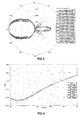
Figure 2 shows the different radiation patterns as a function of the access. -
Figure 3 shows the radiation pattern of the system offigure 1 as a function of frequency. -
Figure 4 shows a curve indicating the impedance matching as a function of frequency for the different radiating elements of the system infigure 1 . - As shown in
figure 1 , in the centre of asubstrate 1 forming a ground plane alens 2 is mounted. Thislens 2 is a part in plastic material, which has been machined or moulded. In the embodiment shows, the lens is made using polymethylmethacrylate or plexiglas which has a permittivity εr = 3.4 and a tangent D = 0.001. However, it is evident to those in the profession that the lens can be produced in other materials such as acrylonitrile-butadiene styrene known under the name ABS or in ceramic or magneto-dielectric materials. - More generally, any material having a permittivity and/or a permeability different from 1 can be used to produce the lens. In the embodiment of
figure 1 , the lens has the shape of a cylindrical ring with a parallelepipedic cross-section, more particularly hexagonal. However, the lens can have a circular ring shape. - As shown in
figure 1 , radiating elements constituted bymonopoles substrate 1 aroundlens 2. Preferentially, these radiating elements are placed symmetrically on a circle to obtain a uniformity of radiation patterns between each other. - In
figure 1 , eachradiating element 31 to 36 is positioned in the middle of one face of the hexagonal lens. Moreover, in the embodiment shown, the monopoles are quarterwave monopoles. Each monopole is associated with areflective element 4 positioned in front of the lens, which enables the radiation of the source to be brought in the direction of the lens. It is evident to a person skilled in the art that the radiating elements can be constituted by elements other than monopoles, namely patches or possibly slots. - According to a characteristic of the present invention, the thickness of the
ring forming lens 2 was optimised to be close to λg/4 where λg is the guided wavelength and is equal to
- A description will now be made of the embodiment according to the configuration of
figure 1 , which was used to conduct simulations by using the 3D electromagnetic software HFSS of the ANSYS company, based on the finite element method. In this case the following dimensions were used. - The substrate is a substrate in a known material FR4 formed by a square of length ∼ 2.75 λ0.
- The distance between the centre of a
reflective strand 4 and the centre of a radiating element is 0.15 λ0. - The distance between a
radiating element 3 and the external wall of thelens 2 is 0.0725 λ0. - The internal diameter of the
lens 2 is 0.4 λ0. - The height of a
reflective strand 4 is 0.3 λ0. - The height of a monopole is 0.25 λ0.
- The height of the plastic lens is 0.367 λ0.
- As shown in
figure 1 , the distance between two diametrically opposed reflectors in relation to an x access is ∼1.12 λ0. - By using the aforementioned dimensions, different patterns and curves shown in
figures 2 to 4 were obtained. -
Figure 2 shows that by exciting the accesses of the sixmonopoles 31 to 36 separately, six standard radiation patterns of the total field are obtained pointing in six different directions of space. Hence, it is possible to cover the entire azimuthal plane while offering a spatial filtering with respect to interfering elements positioned in other angular sectors. To do this, the radiatingelements 31 to 36 can be connected to a switching matrix not shown infigure 1 , which serves as an interface between a MIMO type digital circuit and which enables three sectors among the six available to be chosen. - It is also evident that, in the antenna system of
figure 1 , all the radiating elements can be used simultaneously if necessary. - In
figure 3 , the standard radiation patterns of the total field were shown as a function of frequency for an access between 5GHz and 6GHz. The curves shown infigure 3 show that the radiation remains uniform overall, namely that the opening at +/-30° is respected for an oscillating level between -2.5dB and -4dB with respect to the maximum. - The curves of
figure 4 show that the impedance matching levels are less than -10dB up to a frequency of around 5.75GHz. These levels can be readjusted to cover the entire WiFi band at 5GHz by optimising, for example, the geometry of the lens or by adding an impedance matching network. - The embodiment described above is a simple and low cost embodiment using low cost materials such as a plastic material for the lens, an FR4 type substrate for the substrate and metal strands for the radiating elements and reflective elements. Moreover, the dimensions of the lens, namely the interior and exterior diameters of the ring, the distance between the source and the reflective element, the distance between the wall of the lens as well as the height and position of the lens and the number of sources, make it possible to optimise the directivity and the level of matching in the targeted frequency band.
Claims (7)
- Multibeam antenna system comprising:a substrate (1) forming a ground plane,a lens (2) positioned on the substrate,at least one radiating element (31, 32, 33, 34, 35, 36) to transmit and/or receive electromagnetic waves positioned around the lens, anda switching means enabling the or at least one of the radiating elements to be selected,characterized in that the lens (2) is constituted by a cylindrical ring whose axis is perpendicular to the substrate (1).
- Antenna system according to claim 1, characterized in that the cylindrical ring has in cross-section a circular or parallelepipedic shape.
- Antenna system according to claim 2, characterized in that the circular ring has a thickness close to λg/4 where λg is the guided wavelength, with

- Antenna system according to any one of claims 1 to 3, characterized in that the material of the lens is chosen from among plastic materials such as polymethylmethacrylate (plexiglas), acrylonitrile butadiene styrene (ABS), ceramics, magneto dielectric materials.
- Antenna system according to any one of claims 1 to 4, characterized in that the radiating elements are chosen from among the monopoles, patches, slots.
- Antenna system according to claim 5, characterized in that each monopole positioned near the external surface of the lens is associated with a reflector (4).
- Antenna system according to any one of claims 1 to 6, characterized in that the radiating elements are positioned on a circle circumscribing the lens.
Applications Claiming Priority (1)
| Application Number | Priority Date | Filing Date | Title |
|---|---|---|---|
| FR1154154 | 2011-05-13 |
Publications (2)
| Publication Number | Publication Date |
|---|---|
| EP2523256A1 true EP2523256A1 (en) | 2012-11-14 |
| EP2523256B1 EP2523256B1 (en) | 2013-07-24 |
Family
ID=45888124
Family Applications (1)
| Application Number | Title | Priority Date | Filing Date |
|---|---|---|---|
| EP20120162934 Not-in-force EP2523256B1 (en) | 2011-05-13 | 2012-04-03 | Multibeam antenna system |
Country Status (2)
| Country | Link |
|---|---|
| US (1) | US9147942B2 (en) |
| EP (1) | EP2523256B1 (en) |
Cited By (2)
| Publication number | Priority date | Publication date | Assignee | Title |
|---|---|---|---|---|
| WO2016028869A1 (en) * | 2014-08-21 | 2016-02-25 | Rogers Corporation | Multiple-input, multiple-output antenna with cross-channel isolation using magneto-dielectric material |
| CN107623174A (en) * | 2016-07-14 | 2018-01-23 | 华为技术有限公司 | Di-lens and splitting antenna |
Families Citing this family (8)
| Publication number | Priority date | Publication date | Assignee | Title |
|---|---|---|---|---|
| US9865915B2 (en) * | 2013-02-28 | 2018-01-09 | Apple Inc. | Electronic device with diverse antenna array having soldered connections |
| EP2838162A1 (en) * | 2013-07-17 | 2015-02-18 | Thomson Licensing | Multi-sector directive antenna |
| CN110402521B (en) | 2017-01-13 | 2023-05-30 | 迈特斯因公司 | Multi-beam multiple-input multiple-output antenna system and method |
| US10714827B2 (en) * | 2017-02-02 | 2020-07-14 | The Boeing Company | Spherical dielectric lens side-lobe suppression implemented through reducing spherical aberration |
| US10763916B2 (en) * | 2017-10-19 | 2020-09-01 | At&T Intellectual Property I, L.P. | Dual mode antenna systems and methods for use therewith |
| US20220181052A1 (en) * | 2020-12-04 | 2022-06-09 | Rogers Corporation | Electromagnetic component having magneto-dielectric material |
| US12362460B2 (en) | 2021-05-28 | 2025-07-15 | Matsing, Inc. | Lensed multiple band multiple beam multiple column dual-polarized antenna |
| CN117855866B (en) * | 2024-03-06 | 2024-05-24 | 西安海天天线科技股份有限公司 | High-gain omnidirectional antenna based on metamaterial lens technology |
Citations (2)
| Publication number | Priority date | Publication date | Assignee | Title |
|---|---|---|---|---|
| US6720931B1 (en) * | 2000-04-18 | 2004-04-13 | Hitachi Chemical Co., Ltd. | Planar antenna for beam scanning |
| US20050068251A1 (en) * | 1999-11-18 | 2005-03-31 | Automotive Systems Laboratory, Inc. | Multi-beam antenna |
Family Cites Families (16)
| Publication number | Priority date | Publication date | Assignee | Title |
|---|---|---|---|---|
| US3754270A (en) * | 1972-03-24 | 1973-08-21 | Raytheon Co | Omnidirectional multibeam array antenna |
| US3852761A (en) * | 1973-04-23 | 1974-12-03 | Rca Corp | Lens fed antenna array system |
| SE510565C2 (en) * | 1992-11-10 | 1999-06-07 | Stig Anders Petersson | Vågledarlins |
| DE4430832A1 (en) | 1994-05-23 | 1995-11-30 | Horn Wolfgang | Multiple beam aerial with transmission and receiving equipment |
| EP0877443B1 (en) * | 1997-05-09 | 2008-01-02 | Nippon Telegraph And Telephone Corporation | Antenna and manufacturing method therefor |
| US6081239A (en) * | 1998-10-23 | 2000-06-27 | Gradient Technologies, Llc | Planar antenna including a superstrate lens having an effective dielectric constant |
| US7994996B2 (en) | 1999-11-18 | 2011-08-09 | TK Holding Inc., Electronics | Multi-beam antenna |
| US6424319B2 (en) | 1999-11-18 | 2002-07-23 | Automotive Systems Laboratory, Inc. | Multi-beam antenna |
| JP4181173B2 (en) | 2002-10-24 | 2008-11-12 | サントル ナシオナル ドゥ ラ ルシェルシェサイアンティフィク(セエヌエールエス) | Multi-beam PBG material antenna |
| GB0406814D0 (en) | 2004-03-26 | 2004-08-04 | Bae Systems Plc | An antenna |
| US7898480B2 (en) | 2005-05-05 | 2011-03-01 | Automotive Systems Labortaory, Inc. | Antenna |
| WO2009100153A1 (en) | 2008-02-05 | 2009-08-13 | Ems Technologies, Inc. | Modal beam positioning |
| WO2010016799A1 (en) | 2008-08-07 | 2010-02-11 | Em Technologies Group Pte Ltd | Antenna for omni directional, multi-beam, high gain communication |
| IT1392314B1 (en) | 2008-12-18 | 2012-02-24 | Space Engineering Spa | ANTENNA A LENS DISCRETE ACTIVE APERIODIC FOR MULTI-DRAFT SATELLITE ROOFS |
| EP2376883B1 (en) | 2008-12-19 | 2018-02-28 | Radio Physics Solutions Ltd | A method for formation of radiometric images and an antenna for implementation of the method |
| US8730114B2 (en) * | 2010-06-02 | 2014-05-20 | Mitre Corporation | Low-profile multiple-beam lens antenna |
-
2012
- 2012-04-03 EP EP20120162934 patent/EP2523256B1/en not_active Not-in-force
- 2012-04-27 US US13/458,566 patent/US9147942B2/en not_active Expired - Fee Related
Patent Citations (2)
| Publication number | Priority date | Publication date | Assignee | Title |
|---|---|---|---|---|
| US20050068251A1 (en) * | 1999-11-18 | 2005-03-31 | Automotive Systems Laboratory, Inc. | Multi-beam antenna |
| US6720931B1 (en) * | 2000-04-18 | 2004-04-13 | Hitachi Chemical Co., Ltd. | Planar antenna for beam scanning |
Cited By (4)
| Publication number | Priority date | Publication date | Assignee | Title |
|---|---|---|---|---|
| WO2016028869A1 (en) * | 2014-08-21 | 2016-02-25 | Rogers Corporation | Multiple-input, multiple-output antenna with cross-channel isolation using magneto-dielectric material |
| GB2544212A (en) * | 2014-08-21 | 2017-05-10 | Rogers Corp | Multiple-input, multiple-output antenna with cross-channel isolation using magneto-dielectric material |
| CN107623174A (en) * | 2016-07-14 | 2018-01-23 | 华为技术有限公司 | Di-lens and splitting antenna |
| US11139583B2 (en) | 2016-07-14 | 2021-10-05 | Huawei Technologies Co., Ltd. | Dielectric lens and multi-beam antenna |
Also Published As
| Publication number | Publication date |
|---|---|
| US9147942B2 (en) | 2015-09-29 |
| US20120287005A1 (en) | 2012-11-15 |
| EP2523256B1 (en) | 2013-07-24 |
Similar Documents
| Publication | Publication Date | Title |
|---|---|---|
| EP2523256B1 (en) | Multibeam antenna system | |
| Liang et al. | Cylindrical slot FSS configuration for beam-switching applications | |
| RU2702861C2 (en) | Antenna device and method | |
| Chatterjee et al. | Beamwidth control of omnidirectional antenna using conformal frequency selective surface of different curvatures | |
| EP2053688B1 (en) | Antenna system for wireless digital devices | |
| WO2015192167A1 (en) | Wideband high-gain resonant cavity antenna | |
| WO2020236245A1 (en) | Adaptive mmwave antenna radome | |
| Jeong et al. | Performance improvement of microstrip patch antenna using a novel double‐layer concentric rings metaplate for 5G millimeter wave applications | |
| Brandão et al. | FSS-based dual-band cassegrain parabolic antenna for RadarCom applications | |
| Hassan et al. | Beam divergence reduction of vortex waves with a tailored lens and a tailored reflector | |
| JP6386403B2 (en) | Antenna device | |
| De et al. | Design of an endfire microstrip antenna for aircraft collision avoidance system | |
| CA2912541C (en) | Low profile high efficiency multi-band reflector antennas | |
| Mologni et al. | Investigation on the deployment of FSS as electromagnetic shielding for 5G devices | |
| Parchin et al. | Reconfigurable phased array 5G smartphone antenna for cognitive cellular networks | |
| Simone et al. | 5G wideband stacked patch antennas | |
| CN110546761A (en) | Super-directional array of volumetric antenna elements for wireless device applications | |
| EP2463958A1 (en) | Compact system of multi-beam antennas | |
| Kamarudin et al. | Disc-loaded monopole antenna array for switched beam control | |
| Bertuch et al. | Size-limited Q-band circular switched parasitic array antenna with small elevation beamwidth | |
| CN107768810A (en) | Antenna and its manufacture method | |
| Muqdad et al. | Novel reconfigurable fractal antenna design based metasurface layer for modem wireless systems | |
| JP6747790B2 (en) | Radar equipment | |
| Aremu et al. | Design and Simulation of a 3.5 GHz Pyramidal Horn Antenna for IoT and High Speed 5G Wireless Technology Mobile Networks | |
| KR100994554B1 (en) | Omni variable antenna |
Legal Events
| Date | Code | Title | Description |
|---|---|---|---|
| PUAI | Public reference made under article 153(3) epc to a published international application that has entered the european phase |
Free format text: ORIGINAL CODE: 0009012 |
|
| AK | Designated contracting states |
Kind code of ref document: A1 Designated state(s): AL AT BE BG CH CY CZ DE DK EE ES FI FR GB GR HR HU IE IS IT LI LT LU LV MC MK MT NL NO PL PT RO RS SE SI SK SM TR |
|
| AX | Request for extension of the european patent |
Extension state: BA ME |
|
| 17P | Request for examination filed |
Effective date: 20130107 |
|
| GRAP | Despatch of communication of intention to grant a patent |
Free format text: ORIGINAL CODE: EPIDOSNIGR1 |
|
| RIC1 | Information provided on ipc code assigned before grant |
Ipc: H01Q 21/06 20060101ALI20130215BHEP Ipc: H01Q 15/08 20060101AFI20130215BHEP Ipc: H01Q 19/06 20060101ALI20130215BHEP |
|
| GRAS | Grant fee paid |
Free format text: ORIGINAL CODE: EPIDOSNIGR3 |
|
| GRAA | (expected) grant |
Free format text: ORIGINAL CODE: 0009210 |
|
| AK | Designated contracting states |
Kind code of ref document: B1 Designated state(s): AL AT BE BG CH CY CZ DE DK EE ES FI FR GB GR HR HU IE IS IT LI LT LU LV MC MK MT NL NO PL PT RO RS SE SI SK SM TR |
|
| REG | Reference to a national code |
Ref country code: GB Ref legal event code: FG4D |
|
| REG | Reference to a national code |
Ref country code: CH Ref legal event code: EP |
|
| REG | Reference to a national code |
Ref country code: AT Ref legal event code: REF Ref document number: 623896 Country of ref document: AT Kind code of ref document: T Effective date: 20130815 |
|
| REG | Reference to a national code |
Ref country code: GB Ref legal event code: 746 Effective date: 20130802 Ref country code: IE Ref legal event code: FG4D |
|
| REG | Reference to a national code |
Ref country code: DE Ref legal event code: R096 Ref document number: 602012000152 Country of ref document: DE Effective date: 20130919 |
|
| REG | Reference to a national code |
Ref country code: DE Ref legal event code: R084 Ref document number: 602012000152 Country of ref document: DE Effective date: 20130729 |
|
| REG | Reference to a national code |
Ref country code: AT Ref legal event code: MK05 Ref document number: 623896 Country of ref document: AT Kind code of ref document: T Effective date: 20130724 |
|
| REG | Reference to a national code |
Ref country code: NL Ref legal event code: VDEP Effective date: 20130724 |
|
| REG | Reference to a national code |
Ref country code: LT Ref legal event code: MG4D |
|
| PG25 | Lapsed in a contracting state [announced via postgrant information from national office to epo] |
Ref country code: LT Free format text: LAPSE BECAUSE OF FAILURE TO SUBMIT A TRANSLATION OF THE DESCRIPTION OR TO PAY THE FEE WITHIN THE PRESCRIBED TIME-LIMIT Effective date: 20130724 Ref country code: AT Free format text: LAPSE BECAUSE OF FAILURE TO SUBMIT A TRANSLATION OF THE DESCRIPTION OR TO PAY THE FEE WITHIN THE PRESCRIBED TIME-LIMIT Effective date: 20130724 Ref country code: IS Free format text: LAPSE BECAUSE OF FAILURE TO SUBMIT A TRANSLATION OF THE DESCRIPTION OR TO PAY THE FEE WITHIN THE PRESCRIBED TIME-LIMIT Effective date: 20131124 Ref country code: PT Free format text: LAPSE BECAUSE OF FAILURE TO SUBMIT A TRANSLATION OF THE DESCRIPTION OR TO PAY THE FEE WITHIN THE PRESCRIBED TIME-LIMIT Effective date: 20131125 Ref country code: CY Free format text: LAPSE BECAUSE OF FAILURE TO SUBMIT A TRANSLATION OF THE DESCRIPTION OR TO PAY THE FEE WITHIN THE PRESCRIBED TIME-LIMIT Effective date: 20130918 Ref country code: BE Free format text: LAPSE BECAUSE OF FAILURE TO SUBMIT A TRANSLATION OF THE DESCRIPTION OR TO PAY THE FEE WITHIN THE PRESCRIBED TIME-LIMIT Effective date: 20130724 Ref country code: NO Free format text: LAPSE BECAUSE OF FAILURE TO SUBMIT A TRANSLATION OF THE DESCRIPTION OR TO PAY THE FEE WITHIN THE PRESCRIBED TIME-LIMIT Effective date: 20131024 Ref country code: HR Free format text: LAPSE BECAUSE OF FAILURE TO SUBMIT A TRANSLATION OF THE DESCRIPTION OR TO PAY THE FEE WITHIN THE PRESCRIBED TIME-LIMIT Effective date: 20130724 Ref country code: SE Free format text: LAPSE BECAUSE OF FAILURE TO SUBMIT A TRANSLATION OF THE DESCRIPTION OR TO PAY THE FEE WITHIN THE PRESCRIBED TIME-LIMIT Effective date: 20130724 |
|
| PG25 | Lapsed in a contracting state [announced via postgrant information from national office to epo] |
Ref country code: FI Free format text: LAPSE BECAUSE OF FAILURE TO SUBMIT A TRANSLATION OF THE DESCRIPTION OR TO PAY THE FEE WITHIN THE PRESCRIBED TIME-LIMIT Effective date: 20130724 Ref country code: GR Free format text: LAPSE BECAUSE OF FAILURE TO SUBMIT A TRANSLATION OF THE DESCRIPTION OR TO PAY THE FEE WITHIN THE PRESCRIBED TIME-LIMIT Effective date: 20131025 Ref country code: LV Free format text: LAPSE BECAUSE OF FAILURE TO SUBMIT A TRANSLATION OF THE DESCRIPTION OR TO PAY THE FEE WITHIN THE PRESCRIBED TIME-LIMIT Effective date: 20130724 Ref country code: NL Free format text: LAPSE BECAUSE OF FAILURE TO SUBMIT A TRANSLATION OF THE DESCRIPTION OR TO PAY THE FEE WITHIN THE PRESCRIBED TIME-LIMIT Effective date: 20130724 Ref country code: PL Free format text: LAPSE BECAUSE OF FAILURE TO SUBMIT A TRANSLATION OF THE DESCRIPTION OR TO PAY THE FEE WITHIN THE PRESCRIBED TIME-LIMIT Effective date: 20130724 |
|
| PG25 | Lapsed in a contracting state [announced via postgrant information from national office to epo] |
Ref country code: CY Free format text: LAPSE BECAUSE OF FAILURE TO SUBMIT A TRANSLATION OF THE DESCRIPTION OR TO PAY THE FEE WITHIN THE PRESCRIBED TIME-LIMIT Effective date: 20130724 |
|
| PG25 | Lapsed in a contracting state [announced via postgrant information from national office to epo] |
Ref country code: DK Free format text: LAPSE BECAUSE OF FAILURE TO SUBMIT A TRANSLATION OF THE DESCRIPTION OR TO PAY THE FEE WITHIN THE PRESCRIBED TIME-LIMIT Effective date: 20130724 Ref country code: EE Free format text: LAPSE BECAUSE OF FAILURE TO SUBMIT A TRANSLATION OF THE DESCRIPTION OR TO PAY THE FEE WITHIN THE PRESCRIBED TIME-LIMIT Effective date: 20130724 Ref country code: CZ Free format text: LAPSE BECAUSE OF FAILURE TO SUBMIT A TRANSLATION OF THE DESCRIPTION OR TO PAY THE FEE WITHIN THE PRESCRIBED TIME-LIMIT Effective date: 20130724 Ref country code: SK Free format text: LAPSE BECAUSE OF FAILURE TO SUBMIT A TRANSLATION OF THE DESCRIPTION OR TO PAY THE FEE WITHIN THE PRESCRIBED TIME-LIMIT Effective date: 20130724 Ref country code: RO Free format text: LAPSE BECAUSE OF FAILURE TO SUBMIT A TRANSLATION OF THE DESCRIPTION OR TO PAY THE FEE WITHIN THE PRESCRIBED TIME-LIMIT Effective date: 20130724 |
|
| PG25 | Lapsed in a contracting state [announced via postgrant information from national office to epo] |
Ref country code: IT Free format text: LAPSE BECAUSE OF FAILURE TO SUBMIT A TRANSLATION OF THE DESCRIPTION OR TO PAY THE FEE WITHIN THE PRESCRIBED TIME-LIMIT Effective date: 20130724 Ref country code: ES Free format text: LAPSE BECAUSE OF FAILURE TO SUBMIT A TRANSLATION OF THE DESCRIPTION OR TO PAY THE FEE WITHIN THE PRESCRIBED TIME-LIMIT Effective date: 20130724 |
|
| PLBE | No opposition filed within time limit |
Free format text: ORIGINAL CODE: 0009261 |
|
| STAA | Information on the status of an ep patent application or granted ep patent |
Free format text: STATUS: NO OPPOSITION FILED WITHIN TIME LIMIT |
|
| 26N | No opposition filed |
Effective date: 20140425 |
|
| REG | Reference to a national code |
Ref country code: DE Ref legal event code: R097 Ref document number: 602012000152 Country of ref document: DE Effective date: 20140425 |
|
| PG25 | Lapsed in a contracting state [announced via postgrant information from national office to epo] |
Ref country code: MC Free format text: LAPSE BECAUSE OF FAILURE TO SUBMIT A TRANSLATION OF THE DESCRIPTION OR TO PAY THE FEE WITHIN THE PRESCRIBED TIME-LIMIT Effective date: 20130724 Ref country code: LU Free format text: LAPSE BECAUSE OF FAILURE TO SUBMIT A TRANSLATION OF THE DESCRIPTION OR TO PAY THE FEE WITHIN THE PRESCRIBED TIME-LIMIT Effective date: 20140403 |
|
| REG | Reference to a national code |
Ref country code: IE Ref legal event code: MM4A |
|
| REG | Reference to a national code |
Ref country code: FR Ref legal event code: PLFP Year of fee payment: 4 |
|
| PG25 | Lapsed in a contracting state [announced via postgrant information from national office to epo] |
Ref country code: IE Free format text: LAPSE BECAUSE OF NON-PAYMENT OF DUE FEES Effective date: 20140403 |
|
| PGFP | Annual fee paid to national office [announced via postgrant information from national office to epo] |
Ref country code: DE Payment date: 20150424 Year of fee payment: 4 |
|
| PGFP | Annual fee paid to national office [announced via postgrant information from national office to epo] |
Ref country code: FR Payment date: 20150421 Year of fee payment: 4 |
|
| REG | Reference to a national code |
Ref country code: CH Ref legal event code: PL |
|
| PG25 | Lapsed in a contracting state [announced via postgrant information from national office to epo] |
Ref country code: LI Free format text: LAPSE BECAUSE OF NON-PAYMENT OF DUE FEES Effective date: 20150430 Ref country code: CH Free format text: LAPSE BECAUSE OF NON-PAYMENT OF DUE FEES Effective date: 20150430 |
|
| PG25 | Lapsed in a contracting state [announced via postgrant information from national office to epo] |
Ref country code: MT Free format text: LAPSE BECAUSE OF FAILURE TO SUBMIT A TRANSLATION OF THE DESCRIPTION OR TO PAY THE FEE WITHIN THE PRESCRIBED TIME-LIMIT Effective date: 20130724 |
|
| PG25 | Lapsed in a contracting state [announced via postgrant information from national office to epo] |
Ref country code: SM Free format text: LAPSE BECAUSE OF FAILURE TO SUBMIT A TRANSLATION OF THE DESCRIPTION OR TO PAY THE FEE WITHIN THE PRESCRIBED TIME-LIMIT Effective date: 20130724 |
|
| PG25 | Lapsed in a contracting state [announced via postgrant information from national office to epo] |
Ref country code: RS Free format text: LAPSE BECAUSE OF FAILURE TO SUBMIT A TRANSLATION OF THE DESCRIPTION OR TO PAY THE FEE WITHIN THE PRESCRIBED TIME-LIMIT Effective date: 20130724 Ref country code: BG Free format text: LAPSE BECAUSE OF FAILURE TO SUBMIT A TRANSLATION OF THE DESCRIPTION OR TO PAY THE FEE WITHIN THE PRESCRIBED TIME-LIMIT Effective date: 20130724 |
|
| PG25 | Lapsed in a contracting state [announced via postgrant information from national office to epo] |
Ref country code: SI Free format text: LAPSE BECAUSE OF FAILURE TO SUBMIT A TRANSLATION OF THE DESCRIPTION OR TO PAY THE FEE WITHIN THE PRESCRIBED TIME-LIMIT Effective date: 20130724 Ref country code: HU Free format text: LAPSE BECAUSE OF FAILURE TO SUBMIT A TRANSLATION OF THE DESCRIPTION OR TO PAY THE FEE WITHIN THE PRESCRIBED TIME-LIMIT; INVALID AB INITIO Effective date: 20120403 Ref country code: TR Free format text: LAPSE BECAUSE OF FAILURE TO SUBMIT A TRANSLATION OF THE DESCRIPTION OR TO PAY THE FEE WITHIN THE PRESCRIBED TIME-LIMIT Effective date: 20130724 |
|
| REG | Reference to a national code |
Ref country code: DE Ref legal event code: R119 Ref document number: 602012000152 Country of ref document: DE |
|
| GBPC | Gb: european patent ceased through non-payment of renewal fee |
Effective date: 20160403 |
|
| REG | Reference to a national code |
Ref country code: FR Ref legal event code: ST Effective date: 20161230 |
|
| PG25 | Lapsed in a contracting state [announced via postgrant information from national office to epo] |
Ref country code: FR Free format text: LAPSE BECAUSE OF NON-PAYMENT OF DUE FEES Effective date: 20160502 Ref country code: GB Free format text: LAPSE BECAUSE OF NON-PAYMENT OF DUE FEES Effective date: 20160403 Ref country code: DE Free format text: LAPSE BECAUSE OF NON-PAYMENT OF DUE FEES Effective date: 20161101 |
|
| PG25 | Lapsed in a contracting state [announced via postgrant information from national office to epo] |
Ref country code: MK Free format text: LAPSE BECAUSE OF FAILURE TO SUBMIT A TRANSLATION OF THE DESCRIPTION OR TO PAY THE FEE WITHIN THE PRESCRIBED TIME-LIMIT Effective date: 20130724 |
|
| PG25 | Lapsed in a contracting state [announced via postgrant information from national office to epo] |
Ref country code: AL Free format text: LAPSE BECAUSE OF FAILURE TO SUBMIT A TRANSLATION OF THE DESCRIPTION OR TO PAY THE FEE WITHIN THE PRESCRIBED TIME-LIMIT Effective date: 20130724 |