EP2523203B1 - Switching device and related switchgear - Google Patents
Switching device and related switchgear Download PDFInfo
- Publication number
- EP2523203B1 EP2523203B1 EP11165428.1A EP11165428A EP2523203B1 EP 2523203 B1 EP2523203 B1 EP 2523203B1 EP 11165428 A EP11165428 A EP 11165428A EP 2523203 B1 EP2523203 B1 EP 2523203B1
- Authority
- EP
- European Patent Office
- Prior art keywords
- switching device
- assembly
- movable contact
- semiconductor devices
- fixed contact
- Prior art date
- Legal status (The legal status is an assumption and is not a legal conclusion. Google has not performed a legal analysis and makes no representation as to the accuracy of the status listed.)
- Active
Links
Images




Classifications
-
- H—ELECTRICITY
- H01—ELECTRIC ELEMENTS
- H01H—ELECTRIC SWITCHES; RELAYS; SELECTORS; EMERGENCY PROTECTIVE DEVICES
- H01H9/00—Details of switching devices, not covered by groups H01H1/00 - H01H7/00
- H01H9/54—Circuit arrangements not adapted to a particular application of the switching device and for which no provision exists elsewhere
- H01H9/541—Contacts shunted by semiconductor devices
- H01H9/542—Contacts shunted by static switch means
-
- H—ELECTRICITY
- H01—ELECTRIC ELEMENTS
- H01H—ELECTRIC SWITCHES; RELAYS; SELECTORS; EMERGENCY PROTECTIVE DEVICES
- H01H9/00—Details of switching devices, not covered by groups H01H1/00 - H01H7/00
- H01H9/54—Circuit arrangements not adapted to a particular application of the switching device and for which no provision exists elsewhere
- H01H9/56—Circuit arrangements not adapted to a particular application of the switching device and for which no provision exists elsewhere for ensuring operation of the switch at a predetermined point in the AC cycle
-
- H—ELECTRICITY
- H01—ELECTRIC ELEMENTS
- H01H—ELECTRIC SWITCHES; RELAYS; SELECTORS; EMERGENCY PROTECTIVE DEVICES
- H01H2207/00—Connections
- H01H2207/04—Details of printed conductors
Definitions
- the present disclosure relates to a switching device for connecting/disconnecting an electrical line to/from at least an associated electrical load, and to a switchgear comprising such a switching device.
- switching devices are installed in electrical circuits for connecting/disconnecting a power line to/from one or more associated electrical loads.
- Known switching devices comprise at least a phase, or pole, with a movable contact which is movable between a first connected position, in which it is coupled to a corresponding fixed contact (closed switching device), and a second separated position, in which it is separated from the fixed contact (open switching device).
- a switching device is provided for operatively associating an AC medium voltage line to the bank of capacitors. By opening or closing the switching device, reactive power is added or removed to/from the power line.
- Each phase of the switching device is electrically connected to a power line and the associated electrical load, in such a way that a current can flow between the power line and the load through the main conducting path provided by the coupled fixed and movable contacts.
- the flowing current is interrupted by the separation of the movable contacts from the corresponding fixed contacts, for example in case of faults.
- each phase of the switching device can be provided with a large number of semiconductor devices which are electrically connected in series to each other and are suitable for blocking current flowing therethrough in a blocking direction and for conducting current flowing therethrough in an allowed direction.
- the overall semiconductor devices of a phase are operatively electrically connected in parallel to the main current path provided by the coupled movable contact and the fixed contact.
- the large number of semiconductor devices is due to the fact that each semiconductor device cannot withstand a tension value above a certain limit operation value, typically about 1 kV for standard devices.
- the conductive path provided by the semiconductor devices can be advantageously used for the flowing current, avoiding or at least reducing the generation of electrical arcs during the opening operation of the switching device (when the line is disconnected from a load, e.g. a bank of capacitors), and limiting the inrush current and transient voltages generated during the closing operation (when the line is coupled to the load, e.g. the bank of capacitors).
- WO 01/37300 A1 discloses an electric switching device according to the preamble of claim 1.
- Such device is fulfilled by a switching device for connecting/disconnecting a power line to/from at least an associated electrical load, according to claim 1.
- the switching device in the present disclosure will be described by making particular reference to its application in connecting/disconnecting an AC medium voltage line to/from a bank of capacitors, without intending in any way to limit its possible applications in lower or higher ranges of operating voltages, and/or for different purposes.
- medium voltage used in the present description refers to electrical applications with nominal voltages from 1kV up to some tens of kV, e.g. 52 kV.
- the switching devices according to the present disclosure may be conceived as a hybrid circuit breaker for disconnecting a power line from the associated electrical load, upon the occurrence of electric faults in the circuit, such as a short-circuit fault.
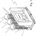
- FIG. 1 illustrates an exemplary embodiment of a multi-phase switching device 1 according to the present disclosure, which is suitable for connecting/disconnecting a power line, for example an AC medium voltage line, to/from at least an associated electrical load.
- a power line for example an AC medium voltage line
- FIG. 1 illustrates an exemplary embodiment of a multi-phase switching device 1 according to the present disclosure, which is suitable for connecting/disconnecting a power line, for example an AC medium voltage line, to/from at least an associated electrical load.
- a power line for example an AC medium voltage line
- the switching device 1 illustrated in figure 1 comprises for example three phases 2, or poles 2, each of which is electrically connected to a corresponding phase of the power line and to an associated electrical load.
- the number of phases 2 may be different to the illustrated one, according to requirements of the specific applications for the switching device 1.
- Each phase 2 comprises a movable contact 4 couplable/separable to/from a corresponding fixed contact 5 (see figures 2-4 ).
- the fixed contact 5 and the movable contact 4 are electrically connected to a first terminal 6 and a second terminal 7, respectively, which are suitable for connecting the phase 2 to the corresponding phase of the power line and of the associated electrical load.
- Each phase 2 comprises an electrically semiconducting assembly (or electric assembly), such as the assembly 50 according to a first exemplary embodiment shown in figures 1-6 , or electric assemblies according to alternative embodiments, such as for example the assembly 200 shown in figures 9-10 .
- the electric assembly has an electrically insulating support operatively associated with a plurality of semiconductor devices 51 electrically connected in series to each other.
- the semiconductor devices 51 are devices suitable for blocking current flowing therethrough in a blocking direction and for conducting current flowing therethrough in an allowed direction.
- Non limiting examples of such semiconductor devices 51 are diodes or thyristors.
- the semiconductor devices 51 are associated and electrically connected to the fixed contact 5 and the movable contact 4 through first connection means and second connection means of the electric assembly, respectively.
- the overall semiconductor devices 51 are able to provide a conductive path for the current flowing through the phase 2; such conductive path is operatively electrically connected in parallel with the main conductive path provided by the coupled fixed and movable contacts 5, 4.
- Each phase 2 comprises a housing 3 for the fixed contact 5 and the movable contact 4, preferably an electrically insulating housing 3 (made for example of epoxy resin) defining a sealed environment filled with electrically insulating gas, such as for example SF 6 or CO 2 or N 2 ; alternatively, the sealed environment defined by the housing 3 may be a vacuum environment.
- electrically insulating housing 3 made for example of epoxy resin
- electrically insulating gas such as for example SF 6 or CO 2 or N 2
- the sealed environment defined by the housing 3 may be a vacuum environment.
- the housing 3 is for example a standard housing for the movable contact and the fixed contact of a medium voltage circuit breaker of known type, such as for example the pole casing of a medium voltage circuit breaker HD4 produced by ABB®.
- the electric assembly is configured to be installed into the housing 3 so as to surround at least a portion of at least one of the fixed contact 5 and the movable contact 4 when it is coupled to the fixed contact 5.
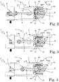
- FIGS 2-4 illustrate the internal part of a housing 3 with an assembly 50 installed therein.
- the movable contact 4 is preferably a piston 4 (or rod 4) actuated by driving means 8 (comprising for example an electric motor associated with a transmission mechanism) so as to move into the housing 3 along an axial direction (indicated in figures 2-4 by the illustrated axis X);
- driving means 8 comprising for example an electric motor associated with a transmission mechanism
- the fixed contact 5 is configured for example as a socket element 5 (or hollow rod 5), suitable for receiving therein a portion of the piston 4.
- the movable contact 4 and the fixed contact 5 may have any other suitable shape or configuration.
- the movable contact 4 is able to assume at least:
- the electric assembly according to the present disclosure is configured for surrounding at least the fixed contact 5.
- the electric assembly may comprise said fixed contact 5 mounted therein.
- the electric assembly is configured for allowing the passage therethrough of the movable contact 4 for coupling/separating to/from the fixed contact 5.
- the electric assembly comprises a hole (see for example the hole 55 of the illustrated assembly 50, or the hole 550 of the illustrated assembly 200) suitable for receiving the fixed contact 5, and extending along the axis X for allowing the passage therethrough of the movable contact 4 in order to couple/separate to/from the fixed contact 5.
- the second connection means of the electric assembly are preferably placed at the entry of the hole for the passage of the movable contact 4, and are configured to operatively contact the movable contact 4 during a portion of its movement.
- the movable contact 4 slides onto the second connection means.
- the electric assembly comprises a foldable printed circuit board 60 with conducting strips 61, made for example of copper, on which the plurality of semiconductor devices 51 is mounted (for example soldered).
- the printed circuit board 60 of the assembly 50 shown in figures 1-6 is rolled by coupling its opposite ends 62, 63 (delimiting its longitudinal extension), so as to feature a substantially cylindrical shape.
- the conducting strips 61 are designed to realize, upon the printed circuit board 60 is rolled, a spiral path for mounting the plurality of semiconductor devices 51 (see in particular the rolled printed circuit board 60 in figure 9 ).
- Figures 7 is a plan view of the unrolled printed circuit board 60, with its conducting strips 61 arranged along three parallel rows 100, 101, 102 extending between the opposite ends 62, 63 of the printed circuit board 60. Rows 100, 101, 102 are defined so as, upon the printed circuit board 60 is rolled, the ends 68, 681 of the rows 102, 101 (placed at the second end 63 of the printed circuit board 60) contact the corresponding ends 67, 671 of the rows 101, 100 (placed at the opposite first end 62 of the printed circuit board 60).
- holes 65 are defined at the ends 68, 681 and are suitable to match, upon the printed circuit board 60 is rolled, with corresponding holes 651 defined at ends 67, 671.
- Securing means such as conductive pins (non visible in the illustrated examples), are inserted through match holes 65-67 so as to block the printed circuit board 60 in the rolled configuration.
- a hole 64 in row 100 and a hole 66 in row 102 delimit, upon the printed circuit board is rolled 60, the spiral path for mounting the plurality of semiconductor devices 51. Therefore, the hole 64 and the hole 66 constitute input/output points for the current flowing through the overall semiconductor devices 51.
- cuts 600 may be defined on the printed circuit board 60 at least between the rows 100-102, so as to increment the electrical insulation between the turns of the spiral path.
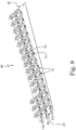
- Figure 8 shows the unrolled printed circuit board 60 of figure 7 , with diodes 51 mounted on the conducting strips 61.
- the series of diodes 51 withstands the operating voltage of the switching device 1, and the number of diodes 51 is such that each diode 51 withstands an operating voltage less than a maximum nominal voltage (about 1.6 kV AC for typical package diodes 51, such as the diodes 51 shown in figure 8 ).
- a maximum nominal voltage about 1.6 kV AC for typical package diodes 51, such as the diodes 51 shown in figure 8 .
- thirty-three standard package diodes 51 are for instance mounted on the printed circuit board 60, each one withstanding, during its operation, a voltage of about 1 kV AC, for applications of the switching device 1 with nominal voltages of about 38 kV AC.
- the number of rows 100, 101, 102 and/or the number of diodes 51 mounted thereon may be different from the illustrated ones; for example the number of diodes 51 shown in figure 8 can be reduced for the switching device 1 operating in lower voltages applications, simply by removing a predefined group of diodes 51 from the corresponding conducting strips 61.
- the switching device 1 may comprise detecting means for monitoring the integrity of diodes 51 and outputting an alarm signal in case of fault conditions.
- semiconductor devices 54 operating as voltage limiting devices 54, are also mounted on the conductive strips 61 of the printed circuit board 60, so as to be electrically in parallel with diodes 51.
- varistors 54 such as for example Zn oxide varistors 54, are used.
- the insulating support of the assembly 50 comprises an electrically insulating box 56 (for example made of plastics) which has a substantially cylindrical shape housing the rolled printed circuit board 60 shown in figure 9 .
- a hole 55 for the passage of the movable contact 4 is defined centrally and along the overall longitudinal extension of the insulating box 56, namely from an upper edge 73 to a lower edge 742 of the insulating box 56.
- the rolled printed circuit board 60 is placed into a seat 69 which is radially defined into the insulating box 56 around the hole 55, and which extends longitudinally between the upper edge 73 and the lower edge 742 of the insulating box 56 (see in particular figure 5 ).
- the seat 69 with the rolled printed circuit board 60 inserted therein, is filled with insulating material, such as resin, to improve the electrical insulation between the turns of the spiral path supporting the diodes 51, and to increase the stability of the structure constituted by printed circuit board 60 and the semiconductor devices 51 (and 54, if present) mounted thereon.
- insulating material such as resin
- the second connection means of the assembly 50 are coupled, preferably fastened, to the superior edge 73 so as to be placed at the entry of the hole 55 for the passage of the movable contact 4.
- the second connection means cover the entry of the hole 55, and are therefore configured for being penetrated by the movable contact 4 entering in or coming out from the hole 55.
- the second connection means comprise at least two conducting plates 74 with through holes 740, and a contact ring 75 between the two plates 74.
- the plates 74 are electrically connected to the plurality of diodes 51 mounted on the rolled printed circuit board 60 in the seat 69, and the contact ring 75 contacts the sliding surface of the movable contact 4 passing through the holes 740 of the discs 74.
- the contact ring 75 is suitable for contacting the movable contact 4 with reduced friction.
- the illustrated assembly 50 further comprises a cover 76 made of insulating material (for example plastics) which is coupled, preferably fastened, to the upper edge 73 of the insulating box 56, so as to cover the plates 74 and the contact ring 75.
- the cover 76 has an inlet 77 for the passage of the movable contact 4 therethrough; preferably, a ring element 82 may be coupled to the edges of the inlet 77 for guiding the passage of the movable contact 4 toward/from the contact ring 75 (see figures 5 and 6 ).
- the assembly 50 comprises a mounting base 59 made of electrically conducting material (for example aluminum) which is suitable for being connected to the first terminal 6 of phase 2, upon the installation of the assembly 50 into the housing 3.
- electrically conducting material for example aluminum
- the fixed contact 5 has a hollow portion 12 for receiving a respective portion of the movable contact 4 (constituted by the piston 4 in the exemplary embodiment shown in figures 2-4 ), and comprises contact rings 10 at the inlet of its hollow portion 12. Contact rings 10 are suitable for improving the contact between the fixed contact 5 and the sliding piston 4.
- the fixed contact 5 is secured to the mounting base 59 through a screw 11.
- the insulating box 56 is mounted on the mounting base 59 in such a way that the fixed contact 5 is inserted into the hole 55; in particular, the insulating box 56 is secured to the mounting base 59 through a plurality of screws 70 (see figures 5 and 6 ).
- the first connection means of the assembly 50 comprises: at least one of the screws 70 which is electrically connected to the overall semiconductor diodes 51 of the printed circuit board 60, and the mounting base 59 connected to the fixed contact 5 and to the terminal 6 of the phase 2.
- the assembly 50 is configured for allowing the passage therethroug of electrically insulating the gas used for filling the housing 3 (after the assembly 50 has been inserted into the housing 3).
- the assembly 50 comprises partitions into the seat 69 (one of which is schematically represented by dashed lines in figure 6 and indicated by numeral reference 700), extending radially with respect to the hole 55, between the upper edge 73 and the lower edge 742 of the insulating box 56.
- At least a vent channel 701 passes through one or more of the partitions 700; the assembly 50 is configured so as said at least one vent channel 701 is accessible from the external of the assembly 50.
- each vent channel 701 is accessible at a first end by through-openings 78 (defined on the edge 73) and through-openings 79 (defined on the cover 76).
- the second end of the vent channels can be operatively connected to means for injecting the electrically insulating gas into the housing 3, for example during manufacturing of the switching device 1.
- the movable contact 4 is inserted in the corresponding hollow portion 12 of the fixed contact 5 (which in turn is inserted into the hole 55 of the assembly 50).
- the coupling between the movable contact 4 and the fixed contact 5 realizes the main conducting path for the current flowing through the phase 2, between the first and second terminals 6, 7.
- the conducting path provided by the overall diodes 51 is short-circuited by the main conducting path provided by the coupled movable contact 4 and fixed contact 5.
- the movable contact 4 When an opening operation of the switching device 1 is required, for example due to a fault or for disconnecting a capacitor bank from the power line associated to the switching device 1, the movable contact 4 is actuated by the driving means 8 so as to spatially separate from the fixed contact 5 (for example, as shown in the exemplary embodiment shown in figures 2-3 , the spatial separation occurs when the movable contact 4 exits the corresponding hollow portion 12 of the fixed contact 5).
- the movement of contact 4 along the illustrated axis X is calibrated so as said spatial separation starts at a first zero-crossing point 500 of the alternate current waveform flowing through phase 2 (see figure 12 ), or a short time (e.g. one or two ms) later with respect to said first zero-crossing point 500.
- a short time e.g. one or two ms
- the current direction allows the conduction by the overall diodes 51 of such current.
- the current flowing through the phase 2 starts flowing through the conducting path provided by the overall diodes 51. In this way the generation of electrical arcs between the fixed contact 5 and the movable contact 4 is avoided or at least substantially reduced.
- the movable contact 4 After the spatial separation from the fixed contact 5, the movable contact 4 continues its movement along axis X, slides onto the contact ring 75 placed at the entry of the hole 55, and arrives at the situation shown in figure 3 . In such a position, the end of the movable contact 4 is still mechanically in contact with the contact ring 75. Therefore, during the sliding from its position shown in figure 4 to its position shown in figure 3 , the movable contact 4 is electrically connected to the overall diodes 51 through the contact ring 75 and the conducting plates 74, so as to allow the current to flow through the phase 2.
- the movable contact 4 continues to slide along the axis X, and spatially separates from the contact ring 75, until it reaches its final position shown in figure 2 , wherein the opening operation of the switching device 1 is concluded.
- the movement of the contact 4 is calibrated so as the spatial separation between the end of the movable contact 4 and the contact ring 75 occurs at a second zero-crossing point 501 of the alternate current waveform, or a short time (e.g. one or two ms) later with respect to said second zero-crossing point 501.
- the second zero-crossing point 501 is consecutive in time to the first zero-crossing point 500; immediately after the second zero-crossing point 501, the current direction blocks the conduction by the overall diodes 51 of such a current.
- the closing operation of the switching devices 1 is the reverse process, starting from the situation shown in figure 2 , wherein no current can flow though phase 2.
- the driving means 8 cause the sliding of the movable contact 4 along the axis X, toward the fixed contact 5.
- the movement of the contact 4 is calibrated so as the end of the movable contact 4 starts mechanically contacting the contact ring 75 (see figure 3 ) a short time (e.g. one or two ms) before said first zero-crossing point 500. In this way, the generation of electrical arcs between the movable contact 4 and the contact ring 75 is avoided or at least substantially reduced.
- the inrush current and the transient voltages are generated when the electrical load associated to the switching device 1 is a bank of capacitors for adding/removing reactive power to/from the power line associated to the switching device 1, according to a first exemplary application of such a switching device 1.
- the movable contact 4 penetrates into the hole 55 of the insulating box 56, until entering into the corresponding hollow portion 12 of the fixed contact 5 (see figure 4 ).
- the movement of the movable contact 4 is calibrated so as the mechanical contact with the fixed contact 5 starts a short time (e.g. one or two ms) before the second zero-crossing point 501 of the current waveform. In this way no electrical arcs are generated between the movable contact 4 and the fixed contact 5, because the current is flowing through the overall diodes 51.
- the conductive path provided by the overall diodes 51 is short-circuited by the re-established main conductive path provided by the coupling of the movable contact 4 with the fixed contact 5.
- the disclosed opening and closing operations could be performed in a second exemplary application of the switching device 1 conceived as a hybrid circuit breaker for breaking currents due to electrical faults.
- high current diodes have to be provided in the assembly 50.
- the insulating support of the assembly in the switching devices 1 may comprise a block of insulating material, for example a casted resin, into which are embedded at least the semiconductor devices 51 (preferably diodes 51) with the electrical connections for electrically connecting in series such semiconductor devices 51 to each other.
- the insulating block may embed also varistors 54 connected electrically in parallel with semiconductor devices 51.
- the insulating block is suitable for being installed into a respective housing 3 of a phase 2 of the switching device 1, preferably so as to completely surround the fixed contact 5.
- the insulating block has a substantially cylindrical shape with a central hole defined along its longitudinal extension; the central hole is suitable for receiving the mobile contact 4 for coupling/separating to/from the fixed contact 5 which is inserted into the central hole.
- the semiconductor devices 51 are embedded into the insulating block of the electric assembly so as to be arranged into the housing 3 along a spiral path extending around the central hole of the insulating block itself.
- the electric assembly of the switching device 1 may have a modular structure, wherein the insulating support for the semiconductor devices 51 of such assembly comprises at least a first modular member and a second modular member mutually coupled.
- the first modular member and the second modular member support a first group and a second group of semiconductor devices 51, respectively, wherein connection means are interposed between the first modular member and the second modular member for electrically connecting in series one to other the first group and the second group of semiconductor devices 51.
- the above mentioned insulating block may be realized as a stack of resin disc portions, each having at least a group of semiconductor devices 51 embedded therein, wherein electrical connection means are provided between adjacent disc portions.
- the assembly 200 is realized as a stack composed by coupling in an alternating way mounting discs 201 (each made of insulating material, such as plastics, and supporting a group of semiconductor devices 51 and, if desired, the respective varistors 54), and covering discs 202 (made of insulating material, such as plastics, and suitable for covering the frontal and rear sides of each mounting disc 201).
- mounting discs 201 each made of insulating material, such as plastics, and supporting a group of semiconductor devices 51 and, if desired, the respective varistors 54
- covering discs 202 made of insulating material, such as plastics, and suitable for covering the frontal and rear sides of each mounting disc 201).
- the assembled stack 200 is suitable for being installed into each housing 3 of the phases 2 of the switching device 1, preferably so as to completely surround the fixed contact 5; as shown in the exemplary embodiment of figure 11 , mounting and covering discs 201, 202 have central holes 203 mutually matching at the coupling of mounting and covering discs 201, 202, so as to form the central hole 550 along the longitudinal extension of the assembly 200.
- the central hole 550 is suitable for receiving the mobile contact 4 for coupling/separating to/from the fixed contact 5, which is inserted into the hole 550.
- Each mounting disc 201 comprises a seat 205 defined around its hole 203, inside which is placed a printed circuit board with the semiconductor devices 51 (and varistors 54, if present) mounted thereon.
- Connections means such as conductive pins 207, pass through the covering discs 202 so as to electrically connect in series one to other the groups of semiconductor devices 51 placed on different mounting discs 201, and so as to provide connection means for the assembly 200 and other parts of the switching device 1.
- Openings 206 are defined in covering discs 202 for the passage therethrough of the gas filling the housing 3.
- the modular structure of the electric assembly guaranties a particular versatility of the switching device 1, since one or more modular members (such as the disc portions of the insulating block, or the mounting discs 201 of the assembly 200) can be added or removed according to the nominal voltages of the specific application of the switching device 1.
- one or more modular members such as the disc portions of the insulating block, or the mounting discs 201 of the assembly 200
- the electric assembly according to the present disclosure allows the insertion of a large number of semiconductor devices 51 (and varistors 54, if present) into the limited volume provided by the housing 3 of the phase 2, keeping a proper distance and insulation between the semiconductor devices 51, and guaranteeing a uniform distribution, across each semiconductor device 51, of the overall voltage applied across the overall series of semiconductor devices 51.
- Particularly suitable for these purposes is the arrangement of semiconductor devices 51 along a spiral path, as in the assembly 50 with the rolled printed circuit board 60.
- the electrical assembly 50, 200 of the switching device 1 is configured to be inserted into a standard pole casing 3 for the movable and fixed contacts of a medium voltage circuit breaker of known type. Therefore, dimensions and electrical power connections of the switching device 1 are those of a standard medium voltage circuit breaker; in this way, the switching device 1 is easily installable in standard cabinets for the medium voltage power distribution.
- all parts/components can be replaced with other technically equivalent elements; in practice, the type of materials, and the dimensions, can be any according to needs and to the state of the art.
- the type of materials, and the dimensions can be any according to needs and to the state of the art.
- different types of diodes can be used, such as for example crimp or screw fixing diodes mounted on suitable supports provided in the electric assembly of the switching device 1; the electric assembly can be realized in a different number of parts, and/or the parts can be differently shaped, and/or differently positioned, and/or differently coupled. It is also possible to perform any combination of the previous embodiments.
Landscapes
- Engineering & Computer Science (AREA)
- Power Engineering (AREA)
- Driving Mechanisms And Operating Circuits Of Arc-Extinguishing High-Tension Switches (AREA)
- Gas-Insulated Switchgears (AREA)
- Breakers (AREA)
Description
- The present disclosure relates to a switching device for connecting/disconnecting an electrical line to/from at least an associated electrical load, and to a switchgear comprising such a switching device.
- As known, switching devices are installed in electrical circuits for connecting/disconnecting a power line to/from one or more associated electrical loads.
- Known switching devices comprise at least a phase, or pole, with a movable contact which is movable between a first connected position, in which it is coupled to a corresponding fixed contact (closed switching device), and a second separated position, in which it is separated from the fixed contact (open switching device). For example, if the electric load is formed by a bank of capacitors, a switching device is provided for operatively associating an AC medium voltage line to the bank of capacitors. By opening or closing the switching device, reactive power is added or removed to/from the power line.
- Each phase of the switching device is electrically connected to a power line and the associated electrical load, in such a way that a current can flow between the power line and the load through the main conducting path provided by the coupled fixed and movable contacts. The flowing current is interrupted by the separation of the movable contacts from the corresponding fixed contacts, for example in case of faults.
- In these known solutions, each phase of the switching device can be provided with a large number of semiconductor devices which are electrically connected in series to each other and are suitable for blocking current flowing therethrough in a blocking direction and for conducting current flowing therethrough in an allowed direction.
- The overall semiconductor devices of a phase are operatively electrically connected in parallel to the main current path provided by the coupled movable contact and the fixed contact. The large number of semiconductor devices is due to the fact that each semiconductor device cannot withstand a tension value above a certain limit operation value, typically about 1 kV for standard devices.
- As known, by opportunely synchronizing the movement of the movable contact to the waveform of the alternate current flowing through the phase of the switching device, the conductive path provided by the semiconductor devices can be advantageously used for the flowing current, avoiding or at least reducing the generation of electrical arcs during the opening operation of the switching device (when the line is disconnected from a load, e.g. a bank of capacitors), and limiting the inrush current and transient voltages generated during the closing operation (when the line is coupled to the load, e.g. the bank of capacitors).
-
WO 01/37300 A1 - At the current state of the art, although known solutions perform in a rather satisfying way, there is still reason and desire for further improvements, in particular as regard to the constructive layout of the semiconducting devices and their positioning relative to the remaining parts of the switching device to which they are associated.
- Such device is fulfilled by a switching device for connecting/disconnecting a power line to/from at least an associated electrical load, according to claim 1.
- In the following description the switching device according to the present disclosure will be described by making particular reference to its application in connecting/disconnecting an AC medium voltage line to/from a bank of capacitors, without intending in any way to limit its possible applications in lower or higher ranges of operating voltages, and/or for different purposes. It is to be set forth that the term "medium voltage" used in the present description refers to electrical applications with nominal voltages from 1kV up to some tens of kV, e.g. 52 kV.
- For example, the switching devices according to the present disclosure may be conceived as a hybrid circuit breaker for disconnecting a power line from the associated electrical load, upon the occurrence of electric faults in the circuit, such as a short-circuit fault.
- Further characteristics and advantages will be more apparent from the description of exemplary, but non-exclusive, embodiments of the switching device according to the present disclosure, illustrated in the accompanying drawings, wherein:
-
figure 1 is a perspective view of a switching device according to the present disclosure; -
figures 2-4 are sectional views showing the inner part of a housing of the switching device infigure 1 , at three different positions assumed by the movable contact; -
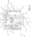
figure 5 is a cross (or section) view of a first embodiment of an electrically semiconducting assembly, which it is suitable for being used in a switching device according to the present disclosure; -
figure 6 is an exploded view of the assembly infigure 5 ; -
figure 7 is a plan view of a printed circuit board used in the assembly offigure 5 ; -
figure 8 is a perspective view of the printed circuit board infigure 7 , with diodes and varistors mounted thereon; -
figure 9 shows the printed circuit board infigure 8 , upon it has been rolled; -
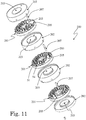
figures 10 and11 are a perspective view and an exploded view, respectively, of a second embodiment of an electrically semiconducting assembly, which is suitable for being installed into a housing of a switching device according to the present disclosure; -
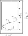
figure 12 shows a period of an alternate current flowing through a phase of a switching device according to the present disclosure. -
Figure 1 illustrates an exemplary embodiment of a multi-phase switching device 1 according to the present disclosure, which is suitable for connecting/disconnecting a power line, for example an AC medium voltage line, to/from at least an associated electrical load. For the sake of simplicity, in the following description reference will be made just to onephase 2 of the switching device 1; however, it is to be understood that what follows is applicable to all thephases 2 of the switching device 1 according to the present disclosure. - The switching device 1 illustrated in
figure 1 comprises for example threephases 2, orpoles 2, each of which is electrically connected to a corresponding phase of the power line and to an associated electrical load. The number ofphases 2 may be different to the illustrated one, according to requirements of the specific applications for the switching device 1. - Each
phase 2 comprises amovable contact 4 couplable/separable to/from a corresponding fixed contact 5 (seefigures 2-4 ). Thefixed contact 5 and themovable contact 4 are electrically connected to afirst terminal 6 and asecond terminal 7, respectively, which are suitable for connecting thephase 2 to the corresponding phase of the power line and of the associated electrical load. - Each
phase 2 comprises an electrically semiconducting assembly (or electric assembly), such as theassembly 50 according to a first exemplary embodiment shown infigures 1-6 , or electric assemblies according to alternative embodiments, such as for example theassembly 200 shown infigures 9-10 . The electric assembly has an electrically insulating support operatively associated with a plurality ofsemiconductor devices 51 electrically connected in series to each other. Thesemiconductor devices 51 are devices suitable for blocking current flowing therethrough in a blocking direction and for conducting current flowing therethrough in an allowed direction. Non limiting examples ofsuch semiconductor devices 51 are diodes or thyristors. - The
semiconductor devices 51 are associated and electrically connected to the fixedcontact 5 and themovable contact 4 through first connection means and second connection means of the electric assembly, respectively. In particular, theoverall semiconductor devices 51 are able to provide a conductive path for the current flowing through thephase 2; such conductive path is operatively electrically connected in parallel with the main conductive path provided by the coupled fixed andmovable contacts - Each
phase 2 comprises ahousing 3 for the fixedcontact 5 and themovable contact 4, preferably an electrically insulating housing 3 (made for example of epoxy resin) defining a sealed environment filled with electrically insulating gas, such as for example SF6 or CO2 or N2; alternatively, the sealed environment defined by thehousing 3 may be a vacuum environment. - The
housing 3 is for example a standard housing for the movable contact and the fixed contact of a medium voltage circuit breaker of known type, such as for example the pole casing of a medium voltage circuit breaker HD4 produced by ABB®. - The electric assembly is configured to be installed into the
housing 3 so as to surround at least a portion of at least one of the fixedcontact 5 and themovable contact 4 when it is coupled to the fixedcontact 5. For example,figures 2-4 illustrate the internal part of ahousing 3 with anassembly 50 installed therein. - According to the exemplary embodiment illustrated in
figures 2-4 , themovable contact 4 is preferably a piston 4 (or rod 4) actuated by driving means 8 (comprising for example an electric motor associated with a transmission mechanism) so as to move into thehousing 3 along an axial direction (indicated infigures 2-4 by the illustrated axis X); thefixed contact 5 is configured for example as a socket element 5 (or hollow rod 5), suitable for receiving therein a portion of thepiston 4. Themovable contact 4 and the fixedcontact 5 may have any other suitable shape or configuration. - The
movable contact 4 is able to assume at least: - a first position, wherein it is mechanically coupled to the fixed contact 5 (for example, in
figure 4 it is inserted into the fixed contact 5); - a second position, wherein it is spatially separated from the fixed contact 5 (for example, in
figures 2-3 it is out from the corresponding hollow portion of the fixed contact 5) and electrically connected to the second connection means of the electric assembly (seefigure 3 ); - a third position, wherein it is spatially separated from the fixed
contact 5 and electrically disconnected from the second connection means of the electric assembly (seefigure 2 ). - The movement of the
contact 4 among these three positions is advantageously synchronized with the waveform of the alternate current flowing through thephase 2, as it will be become more apparent from the following description. - Preferably, the electric assembly according to the present disclosure is configured for surrounding at least the fixed
contact 5. In particular, the electric assembly may comprise said fixedcontact 5 mounted therein. - The electric assembly is configured for allowing the passage therethrough of the
movable contact 4 for coupling/separating to/from the fixedcontact 5. In particular, the electric assembly comprises a hole (see for example thehole 55 of the illustratedassembly 50, or thehole 550 of the illustrated assembly 200) suitable for receiving thefixed contact 5, and extending along the axis X for allowing the passage therethrough of themovable contact 4 in order to couple/separate to/from thefixed contact 5. - The second connection means of the electric assembly are preferably placed at the entry of the hole for the passage of the
movable contact 4, and are configured to operatively contact themovable contact 4 during a portion of its movement. For example, themovable contact 4 slides onto the second connection means. - According to an exemplary embodiment, the electric assembly comprises a foldable printed
circuit board 60 with conductingstrips 61, made for example of copper, on which the plurality ofsemiconductor devices 51 is mounted (for example soldered). - The printed
circuit board 60 of theassembly 50 shown infigures 1-6 is rolled by coupling itsopposite ends 62, 63 (delimiting its longitudinal extension), so as to feature a substantially cylindrical shape. The conductingstrips 61 are designed to realize, upon the printedcircuit board 60 is rolled, a spiral path for mounting the plurality of semiconductor devices 51 (see in particular the rolled printedcircuit board 60 infigure 9 ). -
Figures 7 is a plan view of the unrolled printedcircuit board 60, with its conductingstrips 61 arranged along threeparallel rows opposite ends circuit board 60.Rows circuit board 60 is rolled, theends rows 102, 101 (placed at thesecond end 63 of the printed circuit board 60) contact thecorresponding ends rows 101, 100 (placed at the oppositefirst end 62 of the printed circuit board 60). - In particular,
holes 65 are defined at theends circuit board 60 is rolled, withcorresponding holes 651 defined atends circuit board 60 in the rolled configuration. - Further, a
hole 64 inrow 100 and ahole 66 in row 102 (shown infigure 7 ) delimit, upon the printed circuit board is rolled 60, the spiral path for mounting the plurality ofsemiconductor devices 51. Therefore, thehole 64 and thehole 66 constitute input/output points for the current flowing through theoverall semiconductor devices 51. - Advantageously, cuts 600 (shown for example in dashed lines in
figure 7 ) may be defined on the printedcircuit board 60 at least between the rows 100-102, so as to increment the electrical insulation between the turns of the spiral path. -
Figure 8 shows the unrolled printedcircuit board 60 offigure 7 , withdiodes 51 mounted on the conducting strips 61. The series ofdiodes 51 withstands the operating voltage of the switching device 1, and the number ofdiodes 51 is such that eachdiode 51 withstands an operating voltage less than a maximum nominal voltage (about 1.6 kV AC fortypical package diodes 51, such as thediodes 51 shown infigure 8 ). In the exemplary illustrated embodiment, thirty-threestandard package diodes 51 are for instance mounted on the printedcircuit board 60, each one withstanding, during its operation, a voltage of about 1 kV AC, for applications of the switching device 1 with nominal voltages of about 38 kV AC. - Clearly the number of
rows diodes 51 mounted thereon may be different from the illustrated ones; for example the number ofdiodes 51 shown infigure 8 can be reduced for the switching device 1 operating in lower voltages applications, simply by removing a predefined group ofdiodes 51 from the corresponding conducting strips 61. - The switching device 1 may comprise detecting means for monitoring the integrity of
diodes 51 and outputting an alarm signal in case of fault conditions. - According to an exemplary embodiment,
semiconductor devices 54, operating asvoltage limiting devices 54, are also mounted on theconductive strips 61 of the printedcircuit board 60, so as to be electrically in parallel withdiodes 51. To this end, as shown in the exemplary embodiment offigure 8 ,varistors 54, such as for exampleZn oxide varistors 54, are used. - As shown in the exemplary embodiment of
figures 5 and6 , the insulating support of theassembly 50 comprises an electrically insulating box 56 (for example made of plastics) which has a substantially cylindrical shape housing the rolled printedcircuit board 60 shown infigure 9 . Ahole 55 for the passage of themovable contact 4 is defined centrally and along the overall longitudinal extension of the insulatingbox 56, namely from anupper edge 73 to alower edge 742 of the insulatingbox 56. - The rolled printed
circuit board 60 is placed into aseat 69 which is radially defined into the insulatingbox 56 around thehole 55, and which extends longitudinally between theupper edge 73 and thelower edge 742 of the insulating box 56 (see in particularfigure 5 ). - Advantageously, the
seat 69, with the rolled printedcircuit board 60 inserted therein, is filled with insulating material, such as resin, to improve the electrical insulation between the turns of the spiral path supporting thediodes 51, and to increase the stability of the structure constituted by printedcircuit board 60 and the semiconductor devices 51 (and 54, if present) mounted thereon. - The second connection means of the
assembly 50 are coupled, preferably fastened, to thesuperior edge 73 so as to be placed at the entry of thehole 55 for the passage of themovable contact 4. In particular, the second connection means cover the entry of thehole 55, and are therefore configured for being penetrated by themovable contact 4 entering in or coming out from thehole 55. In particular, as shown in the exemplary embodiment infigures 5 and6 , the second connection means comprise at least two conductingplates 74 with throughholes 740, and acontact ring 75 between the twoplates 74. - The
plates 74 are electrically connected to the plurality ofdiodes 51 mounted on the rolled printedcircuit board 60 in theseat 69, and thecontact ring 75 contacts the sliding surface of themovable contact 4 passing through theholes 740 of thediscs 74. In particular, thecontact ring 75 is suitable for contacting themovable contact 4 with reduced friction. - The illustrated
assembly 50 further comprises acover 76 made of insulating material (for example plastics) which is coupled, preferably fastened, to theupper edge 73 of the insulatingbox 56, so as to cover theplates 74 and thecontact ring 75. Thecover 76 has aninlet 77 for the passage of themovable contact 4 therethrough; preferably, aring element 82 may be coupled to the edges of theinlet 77 for guiding the passage of themovable contact 4 toward/from the contact ring 75 (seefigures 5 and6 ). - The
assembly 50 comprises a mountingbase 59 made of electrically conducting material (for example aluminum) which is suitable for being connected to thefirst terminal 6 ofphase 2, upon the installation of theassembly 50 into thehousing 3. - The fixed
contact 5 has ahollow portion 12 for receiving a respective portion of the movable contact 4 (constituted by thepiston 4 in the exemplary embodiment shown infigures 2-4 ), and comprises contact rings 10 at the inlet of itshollow portion 12. Contact rings 10 are suitable for improving the contact between thefixed contact 5 and the slidingpiston 4. The fixedcontact 5 is secured to the mountingbase 59 through ascrew 11. - The insulating
box 56 is mounted on the mountingbase 59 in such a way that the fixedcontact 5 is inserted into thehole 55; in particular, the insulatingbox 56 is secured to the mountingbase 59 through a plurality of screws 70 (seefigures 5 and6 ). - The first connection means of the
assembly 50 comprises: at least one of thescrews 70 which is electrically connected to theoverall semiconductor diodes 51 of the printedcircuit board 60, and the mountingbase 59 connected to the fixedcontact 5 and to theterminal 6 of thephase 2. - Preferably, the
assembly 50 is configured for allowing the passage therethroug of electrically insulating the gas used for filling the housing 3 (after theassembly 50 has been inserted into the housing 3). In particular, theassembly 50 comprises partitions into the seat 69 (one of which is schematically represented by dashed lines infigure 6 and indicated by numeral reference 700), extending radially with respect to thehole 55, between theupper edge 73 and thelower edge 742 of the insulatingbox 56. - At least a vent channel 701 (such as the
vent channel 701 represented schematically infigure 6 by dashed lines) passes through one or more of thepartitions 700; theassembly 50 is configured so as said at least onevent channel 701 is accessible from the external of theassembly 50. In particular, eachvent channel 701 is accessible at a first end by through-openings 78 (defined on the edge 73) and through-openings 79 (defined on the cover 76). The second end of the vent channels can be operatively connected to means for injecting the electrically insulating gas into thehousing 3, for example during manufacturing of the switching device 1. - An example of the operation of the switching device 1 according to the present disclosure is now disclosed, by making reference to a switching device 1 with the
assembly 50 installed into thehousings 3 of its phase 2 (as illustrated infigures 2-4 ), without in any way precluding the principles of such an operation to switching devices 1 using other alternative embodiments of the electric assembly according to the present disclosure, such as theassembly 200 illustrated infigures 9-10 . - Starting from the situation illustrated in
figure 4 (corresponding to the closed switching device 1), themovable contact 4 is inserted in the correspondinghollow portion 12 of the fixed contact 5 (which in turn is inserted into thehole 55 of the assembly 50). In normal operating conditions, the coupling between themovable contact 4 and the fixedcontact 5 realizes the main conducting path for the current flowing through thephase 2, between the first andsecond terminals overall diodes 51 is short-circuited by the main conducting path provided by the coupledmovable contact 4 and fixedcontact 5. - When an opening operation of the switching device 1 is required, for example due to a fault or for disconnecting a capacitor bank from the power line associated to the switching device 1, the
movable contact 4 is actuated by the driving means 8 so as to spatially separate from the fixed contact 5 (for example, as shown in the exemplary embodiment shown infigures 2-3 , the spatial separation occurs when themovable contact 4 exits the correspondinghollow portion 12 of the fixed contact 5). - The movement of
contact 4 along the illustrated axis X is calibrated so as said spatial separation starts at a first zero-crossing point 500 of the alternate current waveform flowing through phase 2 (seefigure 12 ), or a short time (e.g. one or two ms) later with respect to said first zero-crossing point 500. Immediately after the first zero-crossing point 500, the current direction allows the conduction by theoverall diodes 51 of such current. - Therefore, at the spatial separation between the fixed and
movable contacts phase 2 starts flowing through the conducting path provided by theoverall diodes 51. In this way the generation of electrical arcs between thefixed contact 5 and themovable contact 4 is avoided or at least substantially reduced. - After the spatial separation from the fixed
contact 5, themovable contact 4 continues its movement along axis X, slides onto thecontact ring 75 placed at the entry of thehole 55, and arrives at the situation shown infigure 3 . In such a position, the end of themovable contact 4 is still mechanically in contact with thecontact ring 75. Therefore, during the sliding from its position shown infigure 4 to its position shown infigure 3 , themovable contact 4 is electrically connected to theoverall diodes 51 through thecontact ring 75 and the conductingplates 74, so as to allow the current to flow through thephase 2. - Then, the
movable contact 4 continues to slide along the axis X, and spatially separates from thecontact ring 75, until it reaches its final position shown infigure 2 , wherein the opening operation of the switching device 1 is concluded. - The movement of the
contact 4 is calibrated so as the spatial separation between the end of themovable contact 4 and thecontact ring 75 occurs at a second zero-crossing point 501 of the alternate current waveform, or a short time (e.g. one or two ms) later with respect to said second zero-crossing point 501. As shown infigure 12 , the second zero-crossing point 501 is consecutive in time to the first zero-crossing point 500; immediately after the second zero-crossing point 501, the current direction blocks the conduction by theoverall diodes 51 of such a current. - In this way, the generation of electrical arcs between the second connection means 74, 75 of the
assembly 50 and themovable contact 4 separating from them is avoided or at least substantially reduced. - The closing operation of the switching devices 1 is the reverse process, starting from the situation shown in
figure 2 , wherein no current can flow thoughphase 2. - When the closing of the switching device 1 is required, the driving means 8 cause the sliding of the
movable contact 4 along the axis X, toward the fixedcontact 5. The movement of thecontact 4 is calibrated so as the end of themovable contact 4 starts mechanically contacting the contact ring 75 (seefigure 3 ) a short time (e.g. one or two ms) before said first zero-crossing point 500. In this way, the generation of electrical arcs between themovable contact 4 and thecontact ring 75 is avoided or at least substantially reduced. - Immediately after the first zero-
crossing point 500, current starts flowing thorough theoverall diodes 51 which act limiting the inrush current and transient voltages generated between the phase line and the electrical load associated to thephase 2. - In particular, the inrush current and the transient voltages are generated when the electrical load associated to the switching device 1 is a bank of capacitors for adding/removing reactive power to/from the power line associated to the switching device 1, according to a first exemplary application of such a switching device 1.
- Then, the
movable contact 4 penetrates into thehole 55 of the insulatingbox 56, until entering into the correspondinghollow portion 12 of the fixed contact 5 (seefigure 4 ). The movement of themovable contact 4 is calibrated so as the mechanical contact with the fixedcontact 5 starts a short time (e.g. one or two ms) before the second zero-crossing point 501 of the current waveform. In this way no electrical arcs are generated between themovable contact 4 and the fixedcontact 5, because the current is flowing through theoverall diodes 51. - The conductive path provided by the
overall diodes 51 is short-circuited by the re-established main conductive path provided by the coupling of themovable contact 4 with the fixedcontact 5. - The disclosed opening and closing operations could be performed in a second exemplary application of the switching device 1 conceived as a hybrid circuit breaker for breaking currents due to electrical faults. In this case, high current diodes have to be provided in the
assembly 50. - According to an alternative exemplary embodiment, not illustrate in figures, the insulating support of the assembly in the switching devices 1 may comprise a block of insulating material, for example a casted resin, into which are embedded at least the semiconductor devices 51 (preferably diodes 51) with the electrical connections for electrically connecting in series
such semiconductor devices 51 to each other. The insulating block may embed also varistors 54 connected electrically in parallel withsemiconductor devices 51. - The insulating block is suitable for being installed into a
respective housing 3 of aphase 2 of the switching device 1, preferably so as to completely surround the fixedcontact 5. For example, the insulating block has a substantially cylindrical shape with a central hole defined along its longitudinal extension; the central hole is suitable for receiving themobile contact 4 for coupling/separating to/from the fixedcontact 5 which is inserted into the central hole. - If the insulating block is cast as a monolithic block, preferably the
semiconductor devices 51 are embedded into the insulating block of the electric assembly so as to be arranged into thehousing 3 along a spiral path extending around the central hole of the insulating block itself. - According to another exemplary embodiment, the electric assembly of the switching device 1 according to the present disclosure may have a modular structure, wherein the insulating support for the
semiconductor devices 51 of such assembly comprises at least a first modular member and a second modular member mutually coupled. The first modular member and the second modular member support a first group and a second group ofsemiconductor devices 51, respectively, wherein connection means are interposed between the first modular member and the second modular member for electrically connecting in series one to other the first group and the second group ofsemiconductor devices 51. - For example, the above mentioned insulating block may be realized as a stack of resin disc portions, each having at least a group of
semiconductor devices 51 embedded therein, wherein electrical connection means are provided between adjacent disc portions. - As shown in the alternative exemplary embodiment shown in
figures 10-11 , theassembly 200 is realized as a stack composed by coupling in an alternating way mounting discs 201 (each made of insulating material, such as plastics, and supporting a group ofsemiconductor devices 51 and, if desired, the respective varistors 54), and covering discs 202 (made of insulating material, such as plastics, and suitable for covering the frontal and rear sides of each mounting disc 201). - The assembled
stack 200 is suitable for being installed into eachhousing 3 of thephases 2 of the switching device 1, preferably so as to completely surround the fixedcontact 5; as shown in the exemplary embodiment offigure 11 , mounting and coveringdiscs central holes 203 mutually matching at the coupling of mounting and coveringdiscs central hole 550 along the longitudinal extension of theassembly 200. - The
central hole 550 is suitable for receiving themobile contact 4 for coupling/separating to/from the fixedcontact 5, which is inserted into thehole 550. - Each mounting
disc 201 comprises aseat 205 defined around itshole 203, inside which is placed a printed circuit board with the semiconductor devices 51 (andvaristors 54, if present) mounted thereon. Connections means, such asconductive pins 207, pass through the coveringdiscs 202 so as to electrically connect in series one to other the groups ofsemiconductor devices 51 placed on different mountingdiscs 201, and so as to provide connection means for theassembly 200 and other parts of the switching device 1. -
Openings 206 are defined in coveringdiscs 202 for the passage therethrough of the gas filling thehousing 3. - The modular structure of the electric assembly, according to the two disclosed exemplary embodiments, guaranties a particular versatility of the switching device 1, since one or more modular members (such as the disc portions of the insulating block, or the mounting
discs 201 of the assembly 200) can be added or removed according to the nominal voltages of the specific application of the switching device 1. - In practice, it has been seen how the switching device 1 according to the present disclosure allows offering some improvements over known solutions.
- In particular, the electric assembly according to the present disclosure (such as the illustrate
assembly 50 or the illustrated assembly 200) allows the insertion of a large number of semiconductor devices 51 (andvaristors 54, if present) into the limited volume provided by thehousing 3 of thephase 2, keeping a proper distance and insulation between thesemiconductor devices 51, and guaranteeing a uniform distribution, across eachsemiconductor device 51, of the overall voltage applied across the overall series ofsemiconductor devices 51. Particularly suitable for these purposes is the arrangement ofsemiconductor devices 51 along a spiral path, as in theassembly 50 with the rolled printedcircuit board 60. - Further, the
electrical assembly standard pole casing 3 for the movable and fixed contacts of a medium voltage circuit breaker of known type. Therefore, dimensions and electrical power connections of the switching device 1 are those of a standard medium voltage circuit breaker; in this way, the switching device 1 is easily installable in standard cabinets for the medium voltage power distribution. - Moreover, all parts/components can be replaced with other technically equivalent elements; in practice, the type of materials, and the dimensions, can be any according to needs and to the state of the art. For example, instead of using
standard package diodes 51, different types of diodes can be used, such as for example crimp or screw fixing diodes mounted on suitable supports provided in the electric assembly of the switching device 1; the electric assembly can be realized in a different number of parts, and/or the parts can be differently shaped, and/or differently positioned, and/or differently coupled. It is also possible to perform any combination of the previous embodiments.
Claims (17)
- A switching device (1) for connecting/disconnecting a power line to/from at least an associated electrical load, comprising at least a phase (2) having a housing (3) which houses a movable contact (4) couplable/separable to/from a corresponding fixed contact (5), said phase (2) comprising an electrically semiconducting assembly (50, 200) having a plurality of semiconductor devices (51) electrically connected in series to each other and an insulating support (56, 201) operatively associated with said plurality of semiconductor devices (51), said plurality of semiconductor devices (51) being associated and electrically connected to said fixed contact (5) and being associated and electrically connected to said movable contact (4) during a portion of the movement of said movable contact, said assembly (50) comprising first connection means (70, 59) electrically connecting said plurality of semiconductor devices (51) to the fixed contact (5), and second connection means (74, 75) adapted to electrically connect said plurality of semiconductor devices (51) to the movable contact (4);
wherein said movable contact (4) is able to assume at least:- a first position, wherein said movable contact is coupled to the fixed contact (5);- a second position, wherein said movable contact is spatially separated from the fixed contact (5) and electrically connected to the second connection means (74, 75);- a third position, wherein said movable contact is spatially separated from the fixed contact (5) and electrically disconnected from the second connection means (74, 75);wherein said movable contact moves into the housing along an axial direction (X) of movement to assume said first, second and third positions;
characterised in that said assembly (50, 200) is configured to be installed into said housing (3) so as to surround the fixed contact (5) and allow the passage of the movable contact (4) through said assembly for coupling/separating to/from the fixed contact (5). - The switching device (1) according to claim 1, characterized in that said assembly (50) is configured so as said plurality of semiconductor devices (51) is arranged into said housing (3) along a spiral path.
- The switching device (1) according to one or more of the previous claims, characterized in that said assembly (50) comprises said fixed contact (5) mounted therein.
- The switching device (1) according to one or more of the preceding claims, characterized in that said assembly (50, 200) comprises a hole (55, 204) suitable for receiving the fixed contact (5) and extending along said axial direction (X) for allowing the passage therethrough of the movable contact (4) in order to couple/separate to/from the fixed contact (5).
- The switching device (1) according to claim 4, characterized in that said second connection means (74, 75) of the assembly (50) are placed at the entry of the hole (55) for the passage of the movable contact (4), and are configured to operatively contact the movable contact (4).
- The switching device (1) according to one or more of the preceding claims, characterized in that said assembly (50, 204) is configured for allowing the passage therethrough of electrically insulating gas.
- The switching device (1) according to one or more of the preceding claims, characterized in that said assembly (50) comprises a printed circuit board (60) with conducting strips (61) on which said plurality of semiconductor devices (51) is mounted, wherein said printed circuit board (60) is rolled.
- The switching device (1) according to claim 7, characterized in that said printed circuit board (60) is rolled by coupling its first and second opposite ends (61, 62), wherein said conducting strips (61) are designed to realize a spiral path for mounting the plurality of semiconductor devices (51).
- The switching device (1) according to claim 8, characterized in that said conducting strips (61) are arranged along parallel rows (100, 101, 102) extending between said first and second opposite ends (61, 62) of the printed circuit board (60), wherein said rows (100, 101, 102) are defined so as the end (68, 681) of a row (102, 101) placed at said second end (63) of the printed circuit board (60) is suitable for contacting a corresponding end (67, 671) of an adjacent row (101, 100) placed at said first end (62) of the printed circuit board (60), upon the printed circuit board (60) is rolled.
- The switching device (1) according to claim 9, characterized in that cuts (600) are defined on said printed circuit board (60) between said parallel rows (100, 101, 102).
- The switching device (1) according to one or more of claims 7-10, characterized in that said insulating support (56) comprises an insulating box (56) with a seat (69) suitable for housing said rolled printed circuit board (60).
- The switching device (1) according to claim 11, characterized in that said insulating box (56) comprises partitions (700) extending through the longitudinal extension of the seat (69), wherein at least one vent channel (701) passes through at least one of said partitions, said assembly (50) being configured so as said at least one vent channel (701) is accessible from the external of the assembly (50).
- The switching device (1) according to claim 12, characterized in that said first connection means (70, 59) of the assembly (50) comprise a mounting base (59) onto which the insulating box (56) is mounted and to which the fixed contact (5) is secured, and fixing means (70) for securing the insulating box (56) to the mounting base (59).
- The switching device according to claim 11, characterized in that said assembly (50) comprises an insulating cover (76) which is operatively coupled to said insulating box (56) so as to cover said second connection means (74, 75) and which is configured for allowing the passage therethrough of said movable contact (4).
- The switching device (1) according to one or more of claims 1-6, characterized in that said insulating support comprises at least a block of insulating material into which at least a group of said plurality of semiconductor devices is embedded.
- The switching device (1) according to one or more of claims 1-6, characterized in that said insulating support comprises at least a first modular member (201) and a second modular member (201) mutually coupled, said first modular member (201) and said second modular member (201) supporting a first group and a second group of said plurality of semiconductor devices (51), respectively, wherein connection means (207) are interposed between said first and second modular members (201, 202) for electrically connecting in series said first and second groups of semiconductor devices (51).
- A switchgear comprising at least one switching device (1) according to one or more of the preceding claims.
Priority Applications (7)
| Application Number | Priority Date | Filing Date | Title |
|---|---|---|---|
| PL11165428T PL2523203T3 (en) | 2011-05-10 | 2011-05-10 | Switching device and related switchgear |
| EP11165428.1A EP2523203B1 (en) | 2011-05-10 | 2011-05-10 | Switching device and related switchgear |
| ES11165428T ES2739471T3 (en) | 2011-05-10 | 2011-05-10 | Switching device and related electrical equipment |
| US13/466,496 US9099260B2 (en) | 2011-05-10 | 2012-05-08 | Switching device and related switchgear |
| BR102012010975-1A BR102012010975B1 (en) | 2011-05-10 | 2012-05-09 | switching device and related switching device |
| CN201210144261.1A CN102779666B (en) | 2011-05-10 | 2012-05-10 | Switchgear and relevant switching installations |
| US14/728,275 US9659722B2 (en) | 2011-05-10 | 2015-06-02 | Switching device and related switchgear |
Applications Claiming Priority (1)
| Application Number | Priority Date | Filing Date | Title |
|---|---|---|---|
| EP11165428.1A EP2523203B1 (en) | 2011-05-10 | 2011-05-10 | Switching device and related switchgear |
Publications (2)
| Publication Number | Publication Date |
|---|---|
| EP2523203A1 EP2523203A1 (en) | 2012-11-14 |
| EP2523203B1 true EP2523203B1 (en) | 2019-07-03 |
Family
ID=44816961
Family Applications (1)
| Application Number | Title | Priority Date | Filing Date |
|---|---|---|---|
| EP11165428.1A Active EP2523203B1 (en) | 2011-05-10 | 2011-05-10 | Switching device and related switchgear |
Country Status (6)
| Country | Link |
|---|---|
| US (2) | US9099260B2 (en) |
| EP (1) | EP2523203B1 (en) |
| CN (1) | CN102779666B (en) |
| BR (1) | BR102012010975B1 (en) |
| ES (1) | ES2739471T3 (en) |
| PL (1) | PL2523203T3 (en) |
Families Citing this family (13)
| Publication number | Priority date | Publication date | Assignee | Title |
|---|---|---|---|---|
| US9601284B2 (en) * | 2007-03-14 | 2017-03-21 | Zonit Structured Solutions, Llc | Hybrid relay |
| JP6012713B2 (en) * | 2012-04-06 | 2016-10-25 | 株式会社日立製作所 | Circuit breaker and circuit breaker operating method |
| USD777116S1 (en) * | 2014-09-24 | 2017-01-24 | Abb Technology Ag | Switching device with front cover |
| CN105680706A (en) * | 2014-11-18 | 2016-06-15 | 台达电子工业股份有限公司 | DC power supply device |
| PL3043365T3 (en) | 2015-01-08 | 2018-08-31 | Abb Schweiz Ag | Method and control system for controlling a switching device |
| ES2700835T3 (en) | 2015-07-07 | 2019-02-19 | Abb Technology Ag | Switching device |
| EP3624160B1 (en) | 2018-09-11 | 2022-04-27 | ABB Schweiz AG | A switching device |
| PL3624159T3 (en) | 2018-09-11 | 2021-11-02 | Abb Schweiz Ag | A switching device |
| EP3723110B1 (en) * | 2019-04-12 | 2025-10-29 | ABB Schweiz AG | Synchronized opening of circuit breaker |
| CN110137004A (en) * | 2019-06-04 | 2019-08-16 | 国网四川省电力公司技能培训中心 | A kind of electrical switchgear for power transmission network |
| EP4080725B1 (en) | 2021-04-23 | 2023-12-13 | ABB S.p.A. | Method for estimating the operating conditions of a switching apparatus |
| EP4120307B1 (en) | 2021-07-12 | 2023-11-29 | ABB S.p.A. | A switching apparatus for electric grids |
| EP4227971A1 (en) * | 2022-02-09 | 2023-08-16 | Hitachi Energy Switzerland AG | High voltage disconnector switch |
Family Cites Families (8)
| Publication number | Priority date | Publication date | Assignee | Title |
|---|---|---|---|---|
| GB819717A (en) * | 1954-09-03 | 1959-09-09 | British Thomson Houston Co Ltd | Improvements in electric switches and circuit breakers |
| CH457582A (en) * | 1967-02-21 | 1968-06-15 | Sprecher & Schuh Ag | Vacuum switching device with two working contacts for interrupting alternating current |
| US4393291A (en) * | 1979-10-12 | 1983-07-12 | Brush Switchgear Limited | Gas blast interrupters |
| JPS61260516A (en) * | 1985-05-15 | 1986-11-18 | 日本高圧電気株式会社 | Arc extinguishing for high pressure load switch |
| JPH0770277B2 (en) * | 1990-09-05 | 1995-07-31 | 日本高圧電気株式会社 | High-voltage load switch |
| SE517613C2 (en) * | 1999-11-18 | 2002-06-25 | Abb Ab | Electric coupler for alternating current |
| DE10064525B4 (en) * | 2000-12-22 | 2007-11-08 | Abb Patent Gmbh | Medium voltage switchgear |
| US6888086B2 (en) * | 2002-09-30 | 2005-05-03 | Cooper Technologies Company | Solid dielectric encapsulated interrupter |
-
2011
- 2011-05-10 EP EP11165428.1A patent/EP2523203B1/en active Active
- 2011-05-10 ES ES11165428T patent/ES2739471T3/en active Active
- 2011-05-10 PL PL11165428T patent/PL2523203T3/en unknown
-
2012
- 2012-05-08 US US13/466,496 patent/US9099260B2/en active Active
- 2012-05-09 BR BR102012010975-1A patent/BR102012010975B1/en active IP Right Grant
- 2012-05-10 CN CN201210144261.1A patent/CN102779666B/en active Active
-
2015
- 2015-06-02 US US14/728,275 patent/US9659722B2/en active Active
Non-Patent Citations (1)
| Title |
|---|
| None * |
Also Published As
| Publication number | Publication date |
|---|---|
| BR102012010975A8 (en) | 2017-12-19 |
| US20160042886A1 (en) | 2016-02-11 |
| ES2739471T3 (en) | 2020-01-31 |
| US20120285806A1 (en) | 2012-11-15 |
| CN102779666A (en) | 2012-11-14 |
| US9659722B2 (en) | 2017-05-23 |
| PL2523203T3 (en) | 2019-10-31 |
| CN102779666B (en) | 2016-01-27 |
| BR102012010975A2 (en) | 2016-04-19 |
| EP2523203A1 (en) | 2012-11-14 |
| BR102012010975B1 (en) | 2020-10-13 |
| US9099260B2 (en) | 2015-08-04 |
Similar Documents
| Publication | Publication Date | Title |
|---|---|---|
| US9659722B2 (en) | Switching device and related switchgear | |
| CN201490078U (en) | Conductor components of encapsulated pole units and medium-voltage circuit interrupter comprising components | |
| KR101051113B1 (en) | Vacuum insulated switchgear | |
| US8248760B2 (en) | Switch arrangement for an electrical switchgear | |
| KR100984306B1 (en) | Vacuum Insulated Switch Gear | |
| KR101797414B1 (en) | Current transformer support device, and switchgear using said current transformer support device | |
| EP3143635A1 (en) | Electrical switching apparatus and linear actuator assembly therefor | |
| US8525053B2 (en) | Electrical switchgear | |
| EP2645378B1 (en) | Electric device with insulators | |
| CN107924778A (en) | Switching device | |
| EP3186812A1 (en) | High-voltage combined electrical apparatus | |
| US9418810B2 (en) | Multiphase medium voltage vacuum contactor | |
| RU2345460C2 (en) | High-voltage switchgear of open design | |
| CN101617450B (en) | High-voltage switchgear | |
| EP2495833A1 (en) | Solid insulated busbar arrangement, especially for medium voltage switchgear | |
| JP2010041859A (en) | Solid insulation switch gear | |
| US20170372859A1 (en) | High voltage circuit breaker | |
| US20260018359A1 (en) | Actuator for a Circuit Breaker in a Switchgear | |
| KR102915549B1 (en) | High voltage gas insulated switchgear for single or three-phase operation, HV GIS | |
| JP7488970B2 (en) | Circuit Breakers | |
| US9633756B2 (en) | Device for connecting a circuit breaker | |
| CN111886763B (en) | Compact circuit breaker for gas-insulated switchgear | |
| KR101831850B1 (en) | 25.8KV bypass built-in variable load break switch |
Legal Events
| Date | Code | Title | Description |
|---|---|---|---|
| PUAI | Public reference made under article 153(3) epc to a published international application that has entered the european phase |
Free format text: ORIGINAL CODE: 0009012 |
|
| AK | Designated contracting states |
Kind code of ref document: A1 Designated state(s): AL AT BE BG CH CY CZ DE DK EE ES FI FR GB GR HR HU IE IS IT LI LT LU LV MC MK MT NL NO PL PT RO RS SE SI SK SM TR |
|
| AX | Request for extension of the european patent |
Extension state: BA ME |
|
| 17P | Request for examination filed |
Effective date: 20130513 |
|
| 17Q | First examination report despatched |
Effective date: 20160825 |
|
| STAA | Information on the status of an ep patent application or granted ep patent |
Free format text: STATUS: EXAMINATION IS IN PROGRESS |
|
| RAP1 | Party data changed (applicant data changed or rights of an application transferred) |
Owner name: ABB SCHWEIZ AG |
|
| GRAP | Despatch of communication of intention to grant a patent |
Free format text: ORIGINAL CODE: EPIDOSNIGR1 |
|
| STAA | Information on the status of an ep patent application or granted ep patent |
Free format text: STATUS: GRANT OF PATENT IS INTENDED |
|
| INTG | Intention to grant announced |
Effective date: 20190107 |
|
| GRAS | Grant fee paid |
Free format text: ORIGINAL CODE: EPIDOSNIGR3 |
|
| GRAA | (expected) grant |
Free format text: ORIGINAL CODE: 0009210 |
|
| STAA | Information on the status of an ep patent application or granted ep patent |
Free format text: STATUS: THE PATENT HAS BEEN GRANTED |
|
| AK | Designated contracting states |
Kind code of ref document: B1 Designated state(s): AL AT BE BG CH CY CZ DE DK EE ES FI FR GB GR HR HU IE IS IT LI LT LU LV MC MK MT NL NO PL PT RO RS SE SI SK SM TR |
|
| REG | Reference to a national code |
Ref country code: GB Ref legal event code: FG4D |
|
| REG | Reference to a national code |
Ref country code: CH Ref legal event code: EP Ref country code: AT Ref legal event code: REF Ref document number: 1151983 Country of ref document: AT Kind code of ref document: T Effective date: 20190715 |
|
| REG | Reference to a national code |
Ref country code: DE Ref legal event code: R096 Ref document number: 602011060152 Country of ref document: DE |
|
| REG | Reference to a national code |
Ref country code: IE Ref legal event code: FG4D |
|
| REG | Reference to a national code |
Ref country code: NL Ref legal event code: MP Effective date: 20190703 |
|
| REG | Reference to a national code |
Ref country code: LT Ref legal event code: MG4D |
|
| REG | Reference to a national code |
Ref country code: AT Ref legal event code: MK05 Ref document number: 1151983 Country of ref document: AT Kind code of ref document: T Effective date: 20190703 |
|
| PG25 | Lapsed in a contracting state [announced via postgrant information from national office to epo] |
Ref country code: FI Free format text: LAPSE BECAUSE OF FAILURE TO SUBMIT A TRANSLATION OF THE DESCRIPTION OR TO PAY THE FEE WITHIN THE PRESCRIBED TIME-LIMIT Effective date: 20190703 Ref country code: BG Free format text: LAPSE BECAUSE OF FAILURE TO SUBMIT A TRANSLATION OF THE DESCRIPTION OR TO PAY THE FEE WITHIN THE PRESCRIBED TIME-LIMIT Effective date: 20191003 Ref country code: NO Free format text: LAPSE BECAUSE OF FAILURE TO SUBMIT A TRANSLATION OF THE DESCRIPTION OR TO PAY THE FEE WITHIN THE PRESCRIBED TIME-LIMIT Effective date: 20191003 Ref country code: SE Free format text: LAPSE BECAUSE OF FAILURE TO SUBMIT A TRANSLATION OF THE DESCRIPTION OR TO PAY THE FEE WITHIN THE PRESCRIBED TIME-LIMIT Effective date: 20190703 Ref country code: HR Free format text: LAPSE BECAUSE OF FAILURE TO SUBMIT A TRANSLATION OF THE DESCRIPTION OR TO PAY THE FEE WITHIN THE PRESCRIBED TIME-LIMIT Effective date: 20190703 Ref country code: AT Free format text: LAPSE BECAUSE OF FAILURE TO SUBMIT A TRANSLATION OF THE DESCRIPTION OR TO PAY THE FEE WITHIN THE PRESCRIBED TIME-LIMIT Effective date: 20190703 Ref country code: LT Free format text: LAPSE BECAUSE OF FAILURE TO SUBMIT A TRANSLATION OF THE DESCRIPTION OR TO PAY THE FEE WITHIN THE PRESCRIBED TIME-LIMIT Effective date: 20190703 Ref country code: PT Free format text: LAPSE BECAUSE OF FAILURE TO SUBMIT A TRANSLATION OF THE DESCRIPTION OR TO PAY THE FEE WITHIN THE PRESCRIBED TIME-LIMIT Effective date: 20191104 Ref country code: NL Free format text: LAPSE BECAUSE OF FAILURE TO SUBMIT A TRANSLATION OF THE DESCRIPTION OR TO PAY THE FEE WITHIN THE PRESCRIBED TIME-LIMIT Effective date: 20190703 Ref country code: CZ Free format text: LAPSE BECAUSE OF FAILURE TO SUBMIT A TRANSLATION OF THE DESCRIPTION OR TO PAY THE FEE WITHIN THE PRESCRIBED TIME-LIMIT Effective date: 20190703 |
|
| REG | Reference to a national code |
Ref country code: ES Ref legal event code: FG2A Ref document number: 2739471 Country of ref document: ES Kind code of ref document: T3 Effective date: 20200131 |
|
| PG25 | Lapsed in a contracting state [announced via postgrant information from national office to epo] |
Ref country code: GR Free format text: LAPSE BECAUSE OF FAILURE TO SUBMIT A TRANSLATION OF THE DESCRIPTION OR TO PAY THE FEE WITHIN THE PRESCRIBED TIME-LIMIT Effective date: 20191004 Ref country code: LV Free format text: LAPSE BECAUSE OF FAILURE TO SUBMIT A TRANSLATION OF THE DESCRIPTION OR TO PAY THE FEE WITHIN THE PRESCRIBED TIME-LIMIT Effective date: 20190703 Ref country code: AL Free format text: LAPSE BECAUSE OF FAILURE TO SUBMIT A TRANSLATION OF THE DESCRIPTION OR TO PAY THE FEE WITHIN THE PRESCRIBED TIME-LIMIT Effective date: 20190703 Ref country code: RS Free format text: LAPSE BECAUSE OF FAILURE TO SUBMIT A TRANSLATION OF THE DESCRIPTION OR TO PAY THE FEE WITHIN THE PRESCRIBED TIME-LIMIT Effective date: 20190703 Ref country code: IS Free format text: LAPSE BECAUSE OF FAILURE TO SUBMIT A TRANSLATION OF THE DESCRIPTION OR TO PAY THE FEE WITHIN THE PRESCRIBED TIME-LIMIT Effective date: 20191103 |
|
| PG25 | Lapsed in a contracting state [announced via postgrant information from national office to epo] |
Ref country code: TR Free format text: LAPSE BECAUSE OF FAILURE TO SUBMIT A TRANSLATION OF THE DESCRIPTION OR TO PAY THE FEE WITHIN THE PRESCRIBED TIME-LIMIT Effective date: 20190703 |
|
| PG25 | Lapsed in a contracting state [announced via postgrant information from national office to epo] |
Ref country code: RO Free format text: LAPSE BECAUSE OF FAILURE TO SUBMIT A TRANSLATION OF THE DESCRIPTION OR TO PAY THE FEE WITHIN THE PRESCRIBED TIME-LIMIT Effective date: 20190703 Ref country code: DK Free format text: LAPSE BECAUSE OF FAILURE TO SUBMIT A TRANSLATION OF THE DESCRIPTION OR TO PAY THE FEE WITHIN THE PRESCRIBED TIME-LIMIT Effective date: 20190703 Ref country code: EE Free format text: LAPSE BECAUSE OF FAILURE TO SUBMIT A TRANSLATION OF THE DESCRIPTION OR TO PAY THE FEE WITHIN THE PRESCRIBED TIME-LIMIT Effective date: 20190703 |
|
| PG25 | Lapsed in a contracting state [announced via postgrant information from national office to epo] |
Ref country code: SK Free format text: LAPSE BECAUSE OF FAILURE TO SUBMIT A TRANSLATION OF THE DESCRIPTION OR TO PAY THE FEE WITHIN THE PRESCRIBED TIME-LIMIT Effective date: 20190703 Ref country code: SM Free format text: LAPSE BECAUSE OF FAILURE TO SUBMIT A TRANSLATION OF THE DESCRIPTION OR TO PAY THE FEE WITHIN THE PRESCRIBED TIME-LIMIT Effective date: 20190703 Ref country code: IS Free format text: LAPSE BECAUSE OF FAILURE TO SUBMIT A TRANSLATION OF THE DESCRIPTION OR TO PAY THE FEE WITHIN THE PRESCRIBED TIME-LIMIT Effective date: 20200224 |
|
| REG | Reference to a national code |
Ref country code: DE Ref legal event code: R097 Ref document number: 602011060152 Country of ref document: DE |
|
| PLBE | No opposition filed within time limit |
Free format text: ORIGINAL CODE: 0009261 |
|
| STAA | Information on the status of an ep patent application or granted ep patent |
Free format text: STATUS: NO OPPOSITION FILED WITHIN TIME LIMIT |
|
| PG2D | Information on lapse in contracting state deleted |
Ref country code: IS |
|
| 26N | No opposition filed |
Effective date: 20200603 |
|
| PG25 | Lapsed in a contracting state [announced via postgrant information from national office to epo] |
Ref country code: SI Free format text: LAPSE BECAUSE OF FAILURE TO SUBMIT A TRANSLATION OF THE DESCRIPTION OR TO PAY THE FEE WITHIN THE PRESCRIBED TIME-LIMIT Effective date: 20190703 |
|
| PG25 | Lapsed in a contracting state [announced via postgrant information from national office to epo] |
Ref country code: LI Free format text: LAPSE BECAUSE OF NON-PAYMENT OF DUE FEES Effective date: 20200531 Ref country code: MC Free format text: LAPSE BECAUSE OF FAILURE TO SUBMIT A TRANSLATION OF THE DESCRIPTION OR TO PAY THE FEE WITHIN THE PRESCRIBED TIME-LIMIT Effective date: 20190703 Ref country code: CH Free format text: LAPSE BECAUSE OF NON-PAYMENT OF DUE FEES Effective date: 20200531 |
|
| REG | Reference to a national code |
Ref country code: BE Ref legal event code: MM Effective date: 20200531 |
|
| GBPC | Gb: european patent ceased through non-payment of renewal fee |
Effective date: 20200510 |
|
| PG25 | Lapsed in a contracting state [announced via postgrant information from national office to epo] |
Ref country code: LU Free format text: LAPSE BECAUSE OF NON-PAYMENT OF DUE FEES Effective date: 20200510 |
|
| PG25 | Lapsed in a contracting state [announced via postgrant information from national office to epo] |
Ref country code: IE Free format text: LAPSE BECAUSE OF NON-PAYMENT OF DUE FEES Effective date: 20200510 Ref country code: GB Free format text: LAPSE BECAUSE OF NON-PAYMENT OF DUE FEES Effective date: 20200510 |
|
| PG25 | Lapsed in a contracting state [announced via postgrant information from national office to epo] |
Ref country code: BE Free format text: LAPSE BECAUSE OF NON-PAYMENT OF DUE FEES Effective date: 20200531 |
|
| PG25 | Lapsed in a contracting state [announced via postgrant information from national office to epo] |
Ref country code: MT Free format text: LAPSE BECAUSE OF FAILURE TO SUBMIT A TRANSLATION OF THE DESCRIPTION OR TO PAY THE FEE WITHIN THE PRESCRIBED TIME-LIMIT Effective date: 20190703 Ref country code: CY Free format text: LAPSE BECAUSE OF FAILURE TO SUBMIT A TRANSLATION OF THE DESCRIPTION OR TO PAY THE FEE WITHIN THE PRESCRIBED TIME-LIMIT Effective date: 20190703 |
|
| PG25 | Lapsed in a contracting state [announced via postgrant information from national office to epo] |
Ref country code: MK Free format text: LAPSE BECAUSE OF FAILURE TO SUBMIT A TRANSLATION OF THE DESCRIPTION OR TO PAY THE FEE WITHIN THE PRESCRIBED TIME-LIMIT Effective date: 20190703 |
|
| PGFP | Annual fee paid to national office [announced via postgrant information from national office to epo] |
Ref country code: PL Payment date: 20250506 Year of fee payment: 15 Ref country code: DE Payment date: 20250521 Year of fee payment: 15 |
|
| PGFP | Annual fee paid to national office [announced via postgrant information from national office to epo] |
Ref country code: ES Payment date: 20250627 Year of fee payment: 15 |
|
| PGFP | Annual fee paid to national office [announced via postgrant information from national office to epo] |
Ref country code: IT Payment date: 20250527 Year of fee payment: 15 |
|
| PGFP | Annual fee paid to national office [announced via postgrant information from national office to epo] |
Ref country code: FR Payment date: 20250528 Year of fee payment: 15 |