EP2521222A1 - Multiband antenna - Google Patents
Multiband antenna Download PDFInfo
- Publication number
- EP2521222A1 EP2521222A1 EP12166519A EP12166519A EP2521222A1 EP 2521222 A1 EP2521222 A1 EP 2521222A1 EP 12166519 A EP12166519 A EP 12166519A EP 12166519 A EP12166519 A EP 12166519A EP 2521222 A1 EP2521222 A1 EP 2521222A1
- Authority
- EP
- European Patent Office
- Prior art keywords
- radiating elements
- frequency band
- elements
- ground plane
- dipole
- Prior art date
- Legal status (The legal status is an assumption and is not a legal conclusion. Google has not performed a legal analysis and makes no representation as to the accuracy of the status listed.)
- Granted
Links
- 230000009977 dual effect Effects 0.000 claims description 14
- 239000002184 metal Substances 0.000 claims description 12
- 229910052751 metal Inorganic materials 0.000 claims description 12
- 238000003491 array Methods 0.000 abstract description 7
- 230000010287 polarization Effects 0.000 description 21
- 230000005540 biological transmission Effects 0.000 description 11
- 230000008901 benefit Effects 0.000 description 3
- 238000004519 manufacturing process Methods 0.000 description 3
- 238000000034 method Methods 0.000 description 3
- 230000005855 radiation Effects 0.000 description 2
- 238000000926 separation method Methods 0.000 description 2
- 238000001228 spectrum Methods 0.000 description 2
- WBTMFEPLVQOWFI-UHFFFAOYSA-N 1,3-dichloro-5-(2,5-dichlorophenyl)benzene Chemical compound ClC1=CC=C(Cl)C(C=2C=C(Cl)C=C(Cl)C=2)=C1 WBTMFEPLVQOWFI-UHFFFAOYSA-N 0.000 description 1
- RYGMFSIKBFXOCR-UHFFFAOYSA-N Copper Chemical compound [Cu] RYGMFSIKBFXOCR-UHFFFAOYSA-N 0.000 description 1
- 208000004350 Strabismus Diseases 0.000 description 1
- 230000002411 adverse Effects 0.000 description 1
- 230000033228 biological regulation Effects 0.000 description 1
- 230000015556 catabolic process Effects 0.000 description 1
- 230000010267 cellular communication Effects 0.000 description 1
- 239000004020 conductor Substances 0.000 description 1
- 229910052802 copper Inorganic materials 0.000 description 1
- 239000010949 copper Substances 0.000 description 1
- 238000005388 cross polarization Methods 0.000 description 1
- 230000003247 decreasing effect Effects 0.000 description 1
- 238000006731 degradation reaction Methods 0.000 description 1
- 230000000694 effects Effects 0.000 description 1
- 239000011152 fibreglass Substances 0.000 description 1
- 238000002955 isolation Methods 0.000 description 1
- 230000035515 penetration Effects 0.000 description 1
- 239000004033 plastic Substances 0.000 description 1
- 150000003071 polychlorinated biphenyls Chemical class 0.000 description 1
- 239000000758 substrate Substances 0.000 description 1
- 238000013316 zoning Methods 0.000 description 1
Images





Classifications
-
- H—ELECTRICITY
- H01—ELECTRIC ELEMENTS
- H01Q—ANTENNAS, i.e. RADIO AERIALS
- H01Q1/00—Details of, or arrangements associated with, antennas
- H01Q1/12—Supports; Mounting means
- H01Q1/22—Supports; Mounting means by structural association with other equipment or articles
- H01Q1/24—Supports; Mounting means by structural association with other equipment or articles with receiving set
- H01Q1/241—Supports; Mounting means by structural association with other equipment or articles with receiving set used in mobile communications, e.g. GSM
- H01Q1/246—Supports; Mounting means by structural association with other equipment or articles with receiving set used in mobile communications, e.g. GSM specially adapted for base stations
-
- H—ELECTRICITY
- H01—ELECTRIC ELEMENTS
- H01Q—ANTENNAS, i.e. RADIO AERIALS
- H01Q21/00—Antenna arrays or systems
- H01Q21/06—Arrays of individually energised antenna units similarly polarised and spaced apart
- H01Q21/08—Arrays of individually energised antenna units similarly polarised and spaced apart the units being spaced along or adjacent to a rectilinear path
-
- H—ELECTRICITY
- H01—ELECTRIC ELEMENTS
- H01Q—ANTENNAS, i.e. RADIO AERIALS
- H01Q5/00—Arrangements for simultaneous operation of antennas on two or more different wavebands, e.g. dual-band or multi-band arrangements
- H01Q5/40—Imbricated or interleaved structures; Combined or electromagnetically coupled arrangements, e.g. comprising two or more non-connected fed radiating elements
- H01Q5/42—Imbricated or interleaved structures; Combined or electromagnetically coupled arrangements, e.g. comprising two or more non-connected fed radiating elements using two or more imbricated arrays
Definitions
- Dual band antennas for wireless voice and data communications are known.
- common frequency bands for GSM services include GSM900 and GSM1800.
- GSM900 operates at 880-960 MHz.
- this set of frequencies will be referred to as the "Band 1”.
- GSM1800 operates in the frequency range of 1710-1880MHZ.
- this set of frequencies will be referred to as the "Band 2".
- Antennas for communications in these bands of frequencies typically include an array of radiating elements connected by a feed network.
- the dimensions of radiating elements are typically matched to the wavelength of the intended band of operation. Because the wavelength of the 900MHz band is longer than the wavelength of the 1800MHz band, the radiating elements for one band are typically not used for the other band.
- dual band antennas have been developed which include different radiating elements for the two bands. See, for example, U.S. Patent No. 6,295,028 , U.S. Patent No. 6,333,720 , U.S. Patent No. 7,238,101 and U.S. Patent No. 7,405,710 the disclosures of which are incorporated by reference.
- the radiating elements of the Band 2 may be interspersed with radiating elements of the Band 1, or nested within the radiating elements of the 900 MHz band, or a combination of nesting and interspersing. See, e.g., U.S. Patent 7,283,101 , Fig. 12; U.S. Patent No- 7,405,710 , Fig. 1 , Fig. 7 .
- the radiating elements are typically aligned along a single axis. This is done to minimize any increase in the width of the antenna when going from a single band to a dual band antenna.
- An increase in antenna width may have several undesirable drawbacks.
- a wider antenna may not fit in an existing location or, if it may physically be mounted to an existing tower, the tower may not have been designed to accommodate the extra wind loading of a wider antenna.
- the replacement of a tower structure is an expense that cellular communications network operators would prefer to avoid when upgrading from a single band antenna to a dual band antenna.
- zoning regulations can prevent of using bigger antennas in some areas.
- the UMTS band operates at 1920-2170MHz. This set of frequencies is sufficiently close to the GSM1800 band that UTMS may be considered part of Band 2.
- Digital Dividend spectrum includes 790-862MHz and will be considered hereinafter as part of Band 1.
- additional bands are being added.
- LTE2.6 operates at 2.5-2.7GHz (Hereinafter "Band 3") and WiMax operates at 3.4-3.8GHz (hereinafter "Band 4").
- Bands 3 and 4 wireless communications operators typically replace existing base station antennas with new multiband antennas.
- An object of the present invention is to provide a multiband antenna that includes Band 3 and/or Band 4 capabilities, and has a size comparable to a conventional dual-band antenna, so that it may be installed on existing antenna towers and/or other supports.
- the multiband antenna should be able to operate in three to four bands, which may be well apart from each other.
- Another object of the invention is to provide diversity reception for Band 3 and/or Band 4.
- the multiband antenna has a longitudinal ground plane and several sets of radiating elements mounted on the ground plane, which may be arrayed in linear arrays.
- a first set of first radiating elements may be disposed lengthwise along a center of the ground plane.
- the first radiating elements may be dimensioned to operate in a first frequency band, such as Band 1.
- Band 1 radiating elements are typically dimensioned to operate at about a frequency range of 880-960 MHz, the Digital Dividend spectrum, which is at 790-862MHz, is considered for the purposes of this invention to be part of this band.
- a second set of second radiating elements may also be disposed lengthwise along the center of the ground plane.
- the second radiating elements may be dimensioned to operate in a second frequency band, such as Band 2.
- Band 2 radiating elements are typically dimensioned to operate at about frequency range of 1710-1880MHZ
- the UMTS band which operates at 1920-2170MHz, is considered for the purposes of this invention to be part of this band.
- a third band of frequencies is accommodated by third and fourth sets of radiating elements.
- the third set of third radiating elements is disposed lengthwise on the ground plane on a first side of the first and second sets of radiating elements.
- the third radiating elements may be dimensioned to operate at a third frequency band, such as Band 3 or Band 4.
- the fourth set of fourth radiating elements is disposed lengthwise on the ground plane on a second side of the first and second sets-of radiating elements.
- the fourth radiating elements are also dimensioned to operate in the third frequency band. That is, the third and fourth sets operate in the same band or bands as each other.
- the third and fourth radiating elements are dimensioned to operate at a frequency band of about 2 .5 - 2.7 GHz. In another example, the third and fourth radiating elements are dimensioned to operate at a frequency band of about 3.4 -- 3.8 GHz.
- the third and fourth radiating elements are directed dipole elements.
- the directed dipole elements may be of a conventional Yagi style configuration, or a twisted configuration to provide circular polarization.
- the directed dipoles may be fabricated on a printed circuit board or fabricated from sheet metal, such as the ground plane. In these examples, an entire set of radiating elements may be fabricated as a single unit.
- the third and fourth radiating elements comprise +/- 45 degree polarized dipole elements.
- the longitudinal ground plane may further comprise a center well and first and second outer wells.
- the first set of first radiating elements and the second set of second radiating elements are disposed in the center well.
- the third set of third radiating elements is disposed in the first outer well, and the fourth set of fourth radiating elements are disposed in the second outer well.
- the wells enable use of+/- 45 degree polarization on the third and fourth sets of radiating elements without causing undue interference with the first and second sets of radiating elements.
- the outer wells may be angled inward to adjust performance.
- a four-band antenna is provided.
- the multiband antenna further includes a fifth set of fifth radiating elements interspersed with the third radiating elements, the fifth radiating elements being dimensioned to operate at a fourth frequency band, and a sixth set of sixth radiating elements interspersed with the fourth radiating elements, the sixth radiating elements being dimensioned to operate in the fourth frequency band.
- the first frequency band comprises about 790-960 MHz
- the second frequency, band comprises about 1710-2170 MHz
- the third frequency band comprises about 2.5 - 2.7 GHz
- the fourth frequency band comprises about 3.4 - 3.8 GHz.
- a multiband antenna includes a ground plane and a plurality of radiating elements.
- the ground plane may be a single sheet metal stamping.
- a multiband antenna 10 has four sets of radiating elements mounted on a ground plane 12,
- a first set of radiating elements 14 comprises a first linear array of microstrip annular ring elements 14a arranged on a longitudinal axis, approximately in the center of the ground plane 12.
- the microstrip annular ring elements 14a are dimensioned to efficiently transmit and/or receive RF signals in Band 1.
- the first set of radiating elements comprises low band elements.
- the second set of radiating elements 16 comprises a second linear array of crossed dipole elements 16a, 16b.
- the crossed dipole elements 16a, 16b are also arranged in the center of the ground plane 12 on the longitudinal axis approximately in the center of the ground plane 12.
- the crossed dipole elements are dimensioned for transmission and/or reception of RF signals, in Band 2.
- the crossed dipole elements 16a may be interspersed with the annular ring elements. Additionally, or alternately, the crossed dipole elements 16b may be nested within the microstrip annular ring elements.
- the cross dipole elements may be oriented so that the dipole elements are at approximately +45 degrees to vertical and -45 degrees to vertical to provide polarization diversity reception.
- the annular ring elements have two ⁇ 45 degree polarizations, and may be used to provide polarization diversity, also.
- box dipole elements may be substituted for the crossed dipole elements 16a, 16b.
- box dipole elements may be substituted for the microstrip annular ring elements 14a.
- dual-polarized patch elements can be used for Band 1 and Band 2 (as in U.S. Patent 6,295,028 ).
- a third set of radiating elements 20 may comprise an array of radiating elements 20a.
- the third radiating elements 20a comprise directed dipole elements. These are commonly known as Yagi-Uda style radiating elements.
- the third set of radiating elements 20 is located near the outer edge of the ground plane 12.
- the third set of radiating elements 20 and the fourth set of radiating elements 26 may be fabricated from sheet metal.
- the feed network may comprise airstrip conductors on one or both sides of the ground plane 32. See, e.g., Fig. 5 .
- a phase shifter (PCB or airstrip) may also be mounted on the ground plane 12 and coupled to the airstrip feed lines as shown schematically in Fig. 5 .
- An advantage of this example is that no additional supports are necessary for the directors, and the cost of the third and fourth sets of radiating elements is significantly reduced.
- the third radiating elements 20a are dimensioned for transmission and reception of RF signals in Band 3 or Band 4.
- third radiating element 20a comprises a directed dipole, including a dipole support 30 extending from a ground plane 32, and a director support 31 extending further from the dipole support 30.
- Director support 31 and dipole support 30 further include a 0.5 wavelength balun slot 34.
- Dipole 36 is supported by the dipole support 30.
- Dipole 36 is perpendicular to balun slot 34.
- directors 38a, 38b, 38c are supported above the dipole 36 by director support 31.
- One end of balun slot 34 is near the beginning of director 38a, and the other end is near the beginning of ground plane 32.
- Providing balun slot 34 renders the director support 31 between the dipole 36 and first director 38a invisible with respect to RF signals.
- Airstrip line 40 is provided to excite the radiating element 20a. Airstrip line 40 crosses balun slot 34 near the center of balun slot 34. Airstrip line 40 may be supported off the ground plane 32 and dipole support 30 by plastic supports to provide an air dielectric.
- the ground plane 32, dipole support 30, director support 31, dipole 36, and directors 38a, 38b, 38c may be fabricated from a single piece of sheet metal.
- the third and fourth sets of radiating elements may be formed integrally with ground plane 12. While other fabrication techniques may be used to construct directed dipoles of radiating element 20a, the stamped metal example has certain advantageous aspects. All of the components (dipole, directors, supports, ground plane) of many directed dipole elements may be fabricated as a single piece. This saves cost and assembly time.
- a fourth set of radiating elements 26 may comprise an array of directed dipole elements arranged along an edge of the ground plane 12 opposite the third set of radiating elements 20.
- the fourth set of radiating elements 26 are fabricated to be the same as the third set of radiating elements 20.
- the fourth radiating elements 26a are directed dipole elements which are dimensioned to be the same as the third set of radiating elements, and the feed network is equivalent.
- the radiating elements 20a of third set of radiating elements 20 are dimensioned for transmission and/or reception of RF signals in Band 3, so are the fourth radiating elements 26a of the fourth set of radiating elements 26.
- the third and fourth sets of radiating elements are fabricated on a Printed Circuit Boards (PCB).
- a feed network may be fabricated on the PCB.
- the feed network may include variable elements, such as phase shifters, to adjust antenna radiation attributes, such as beam tilt.
- the feed network may also include a diplexer (e.g., between Band 1 and Band 3 or 4).
- the distance between the third set of radiating elements 20 and the fourth set of radiating elements 26 may be in the range of 1.5 to 4 wavelengths of the Band 3 or Band 4 signals to allow for space diversity with correlation coefficient ⁇ 0.5 and diversity gain >8dB.
- the distance between the third set of radiating elements 20 and the fourth set of radiating elements 26 may be in the range of 1.5 to 4 wavelengths of the Band 3 or Band 4 signals to allow for space diversity with correlation coefficient ⁇ 0.5 and diversity gain >8dB.
- a typical Base station dual-band antenna has a width of about 300mm. Accordingly, preferably, the third and fourth radiating elements are located near the outer edges of the ground plane 12, to achieve a separation of about 2.2 wavelengths of Band 3.
- the directed dipole arrangement of the example give above has been found to operate satisfactorily without causing undesirable levels of interference with the first and second sets of radiating elements (e.g., Band 1 and Band 2). Thanks to small electrical size of directed dipole for Band 1, 2.
- baffles may be included between the Band 1 and Band 2 elements and the Band 3 and/or Band 4 elements. Baffles may improve F/B and symmetry of the radiated pattern.
- azimuth beam width can be adjusted, matching with beam width of Band 1, Band 2. For example, a 65 degree beam requires 3-5 directors.
- high directive Yagi style elements (with element pattern of ⁇ 60 degree in azimuth and ⁇ 45 degree in elevation, which can be achieved with 5-6 directors) elements are used.
- the high directive elements allow an increase in spacing between elements (up to 1.2 wavelength) and reduces the number of elements required by 30% compared to regular dipole radiating elements. This provides a further cost savings.
- the third and fourth sets of radiating elements may comprise Yagi-style directed elements with circular polarization.
- Elements 14, 16 in Figure 4 that are the same as elements in Figure 1 receive the same reference characters, and the discussion of these elements is not repeated here.
- Radiating element 44a comprises a directed dipole, including a dipole support 50 extending from a ground plane 52, and a director support 51 extending further from the dipole support 50.
- Director support 51 and dipole support 50 further include a 0.5 wavelength balun slot 54
- Dipole 56 is supported by the dipole support 50.
- Dipole 56 is perpendicular to balun slot 54.
- directors 58a, 58b, 58c, 58d, 58e are supported above the dipole 56 by director support 51.
- the directors 58a, 58b, 58c, 58d, 58e are not located in the same plane as the dipole 56 (as in known Yagi antennas) of the radiating elements 44a, but are gradually rotated from a vertical position to a horizontal position, Additionally, the directors 58a-58e may be rotated to achieve orthogonal polarizations for the third and fourth sets of radiating elements 44, 46.
- the third radiating elements 44a may have the directors 58a-58e rotated to the right (clockwise), while the fourth radiating elements 46a may have the directors rotated to the left (counter clockwise).
- the circularly polarized elements may be constructed as elements fabricated from a metal stamping or in accordance with any other examples described herein, e.g., as PCBs or as a single stamping integral with the ground plane 12.
- the combination of space diversity and polarization diversity leads to very low correlation and good diversity gain.
- circular polarization is known for good in-building penetration and less mismatch with handsets.
- each director is rotated at an angle ⁇ with respect to the immediately preceding director.
- Director 58a adjacent to the dipole 56, is rotated at an angle ⁇ with respect to the dipole 56.
- the angle ⁇ may be constant or variable.
- the angle ⁇ may be in the range of about 5 degrees to 25 degrees.
- Figure 3 illustrates that a circularly polarized directed-dipole element may be fabricated from a single sheet metal stamping. This is in contrast to conventional circular polarization schemes, which involves a quadrature coupler and two sets of orthogonal dipoles.
- an assembly may include both Band 3 radiating elements 60 and Band 4 radiating elements 62.
- including both Band 3 and Band and Band 4 radiating elements 60, 62 means that a fifth set of radiating elements and a sixth set of radiating elements are provided.
- the third and fourth sets of radiating elements comprise directed dipole elements are dimensioned for efficient transmission and reception of Band 3 RF signals.
- the radiating elements comprising the fifth and sixth sets of radiating elements are also directed dipole elements, and are dimensioned for efficient transmission and reception of RF signals in Band 4.
- the fifth set of radiating elements may be interspersed with the third set of radiating elements, and the sixth set of radiating elements may be interspersed with the fourth set of radiating elements.
- the spacing for each radiating element in each band can be about 100 mm (1.2 wavelength for Band 4 and 0.9 wavelength for Band 3), allowing Band 4 elements to be placed between Band 3 elements. Thanks to narrow element pattern of directed dipole in elevation plane, grating lobes are ⁇ -10dB in Band 3, 4 with beam tilts up to 10°. In this manner, low cost antenna is realized with 8 connectors/ports, and with width ⁇ 300mm only.
- the third, fourth, fifth and sixth sets of radiating elements may comprise any of the configurations and manufacturing techniques described above, e.g., vertically oriented directed dipoles, circularly polarized directed dipoles, and/or PCB radiating elements and feed networks or directed dipoles fabricated in one piece with the ground plane 12.
- FIG. 5 an example using directed dipole fabricated integrally with the ground plane is shown.
- the microstrip feed network 64 for the Band 3 elements is shown, but, the microstrip feed network for the Band 4 elements is on the opposite side of the ground plane 32 and is not shown.
- Diplexers may be integrated in to reduce the number of antenna connectors.
- PCB Printed Circuit Board
- the PCB 72 includes a plurality of directed dipoles 74, which are plated copper on a glass-reinforced plastic substrate. Also illustrated is a feed network 76 for the radiating elements disposed on the PCB.
- multiband antenna 110 in Figure 6 , it may be desired to use conventional slant ⁇ 45 polarization for all bands without the use of Yagi-style directed dipoles.
- a ground plane 112 and a plurality of radiating elements is provided.
- the ground plane 112 may comprise a center well 170 and a first outer well 172 and a second outer well 172.
- the ground plane 112 may be a single sheet metal stamping, or the center well 170 and outer wells 172 may be defined by walls or baffles.
- a first set of radiating elements 114 comprises a first linear array of first patch radiating elements 114a arranged on a longitudinal axis, approximately in the center of the ground plane 112.
- the first patch elements are dimensioned to efficiently transmit and/or receive RF signals in Band 1.
- the second set of radiating elements 116 comprises a second linear array of second patch elements 116a.
- the second patch elements are also arranged in the center well 170 on the longitudinal axis approximately in the center of the ground plane 112.
- the second patch elements are dimensioned for transmission and/or reception of RF signals, in Band 2.
- the second patch elements may be interspersed with the first patch elements. In alternate examples, the second patch elements may be nested within the first patch elements.
- band 1 and 2 other types of dual polarized radiating elements can be used for Band 1 and 2; for example microstrip annular ring, box dipole, and/or crossed dipoles.
- a third set of radiating elements 124 may comprise an array of dipole radiating elements 124a, arranged at an angle of+45° to the longitudinal axis of the ground plane 112, and disposed in the first outer well 172.
- the third set of radiating elements 124 are dimensioned for transmission and reception of RF signals in Band 3 or Band 4.
- a fourth set of radiating elements 126 may comprise an array of dipole radiating elements 126a, arranged a -45°angle to the longitudinal axis of the ground plane 112, and disposed in the second outer well 172.
- the dipole elements of the fourth set of radiating elements are dimensioned to be the same as the dipole elements of the third set of radiating elements, only oriented so that the polarization is 90° to the third set of radiating elements. For example, if the dipole elements of third set of radiating elements are dimensioned for transmission and/or reception of RF signals in Band 3, so are the dipole elements of the fourth set of radiating elements.
- both polarization diversity ( ⁇ 45 degree) and space diversity (with spacing about 2.2 wavelength) are achieved for Band 3 (or Band 4), providing reduction of correlation coefficient and increasing of diversity gain.
- the use of the first and second outer wells 172 enables the use of conventional dipole elements at 45 degree slants, without adversely affecting the performance of the Band 1 and Band 2 elements.
- first outer well 172 and the second outer well 172 are approximately parallel with the center well 170.
- multiband antenna 2100 is illustrated.
- ground plane 212 is formed such that the first and second outer wells 272 are angled inward with respect to center well 270.
- rotation of the outer wells 172 improves pattern squint of Band 3 and Band 4 and without degradation of Band 3 (4) radiation pattern due to edge effect.
- wells 172 are improving front-to-back and cross-polarization ratios for Band 3 (4).
- multiband antenna 310 has a center well 370 and outer wells 372.
- Third set of radiating elements 324 and fifth set of radiating elements 344 are disposed in a first outer well 372, while fourth set of radiating elements 326 and sixth set of radiating elements 346 are disposed in a second outer well 372.
- the third and fourth sets of radiating elements 324, 326 are Band 3 radiating elements
- the fifth and sixth sets of radiating elements 344, 346 are Band 4 radiating elements.
- Directors can be used above dipoles 326, 346 for decreasing interference between them.
- the radiating elements 324a may be staggered with respect to radiating elements 344a, and radiating elements 326a may be staggered with respect to radiating elements 346a, so that they do not share a common axis, and/or may be offset from the center of the outer well 372.
- the multiband antenna may have only Band 3 or Band 4 elements, and the radiating elements within a set of radiating elements may be offset with respect to each other. This provides further improvement of beam stability and narrows azimuth beam width to 60-65°.
- the third set of radiating elements comprises an array of box dipole elements disposed in the first outer well.
- the third set of radiating elements are dimensioned for efficient transmission and reception of RF signals in Band 3.
- the fourth set of radiating elements comprises an array of box dipole elements disposed in the second outer well.
- the fourth set of radiating elements are dimensioned for efficient transmission and reception of R.F signals in Band 4.
- a four-band 8-port antenna is realised.
- the third set of radiating elements and the fourth set of radiating elements need not be box dipole elements.
- the third set of radiating elements may comprise box dipole elements and the fourth set of radiating elements may comprise cross dipole elements. Other combinations of radiating elements are contemplated, including dipole of Band 3 crossed with dipole of Band 4.
- third and forth sets of radiating elements 424, 426 are identical dual polarized arrays of Band 3 (or Band 4) elements.
- This 3-band antenna has 8 ports (2 ports for Band 1, 2 ports for Band 2, 4 ports for Band 3 (or 4).
- Radiating elements of third and forth sets 424a, 426a are located in first and second outer wells 472 respectively, and can be +/-45 polarized cross-dipoles, box dipoles, (as shown in Fig. 9 ), or patch elements. Due to orthogonally of polarizations and physical separation between these 2 identical arrays, very low correlation coefficient between them is achieved, which benefits to LTE2.6 performance and using of 4x2 and 4x4 multiple-output (MIMO) schemes. Also, placing of 2 identical arrays for the same base station sector increases system capacity and throughput.
- MIMO multiple-output
Landscapes
- Engineering & Computer Science (AREA)
- Computer Networks & Wireless Communication (AREA)
- Physics & Mathematics (AREA)
- Electromagnetism (AREA)
- Variable-Direction Aerials And Aerial Arrays (AREA)
- Aerials With Secondary Devices (AREA)
Abstract
Description
- Dual band antennas for wireless voice and data communications are known. For example, common frequency bands for GSM services include GSM900 and GSM1800. GSM900 operates at 880-960 MHz. Hereinafter, this set of frequencies will be referred to as the "Band 1". GSM1800 operates in the frequency range of 1710-1880MHZ. Hereinafter, this set of frequencies will be referred to as the "Band 2".
- Antennas for communications in these bands of frequencies typically include an array of radiating elements connected by a feed network. For efficient transmission and reception of Radio Frequency (RF) signals, the dimensions of radiating elements are typically matched to the wavelength of the intended band of operation. Because the wavelength of the 900MHz band is longer than the wavelength of the 1800MHz band, the radiating elements for one band are typically not used for the other band. In this regard, dual band antennas have been developed which include different radiating elements for the two bands. See, for example,
U.S. Patent No. 6,295,028 ,U.S. Patent No. 6,333,720 ,U.S. Patent No. 7,238,101 andU.S. Patent No. 7,405,710 the disclosures of which are incorporated by reference. - In these known dual band antennas, the radiating elements of the Band 2 may be interspersed with radiating elements of the Band 1, or nested within the radiating elements of the 900 MHz band, or a combination of nesting and interspersing. See, e.g.,
U.S. Patent 7,283,101 , Fig. 12;U.S. Patent No- 7,405,710 ,Fig. 1 ,Fig. 7 . In these known dual-band antennas, the radiating elements are typically aligned along a single axis. This is done to minimize any increase in the width of the antenna when going from a single band to a dual band antenna. - An increase in antenna width may have several undesirable drawbacks. For example, a wider antenna may not fit in an existing location or, if it may physically be mounted to an existing tower, the tower may not have been designed to accommodate the extra wind loading of a wider antenna. The replacement of a tower structure is an expense that cellular communications network operators would prefer to avoid when upgrading from a single band antenna to a dual band antenna. Also, zoning regulations can prevent of using bigger antennas in some areas.
- Known dual band antennas, while useful, are not sufficient to accommodate future traffic demands. Wireless data traffic is growing dramatically in various global markets. There are growing number of data service subscribers and increased traffic per subscriber. This is due, at least in part, to the growing popularity of "smart phones," such as the iPhone, Android-based devices, and wireless modems. The increasing demand of wireless data is exceeding the capacity of the traditional two-band wireless communications networks.
- To address this increasing demand, wireless network operators are adding new wireless bands of frequencies. For example, the UMTS band operates at 1920-2170MHz. This set of frequencies is sufficiently close to the GSM1800 band that UTMS may be considered part of Band 2. Also, Digital Dividend spectrum includes 790-862MHz and will be considered hereinafter as part of Band 1. However, additional bands are being added. For example, LTE2.6 operates at 2.5-2.7GHz (Hereinafter "Band 3") and WiMax operates at 3.4-3.8GHz (hereinafter "Band 4"). To make use of Bands 3 and 4, wireless communications operators typically replace existing base station antennas with new multiband antennas.
- However, simply adding additional cross-polarized radiating elements for Band 3 and Band 4 to a conventional dual band antenna poses certain difficulties. There is limited area for the inclusion of additional radiating elements, because the space between radiating elements of one band is already occupied by radiating elements of another band. Also, the Band 3 and Band 4 elements may introduce undesirable interference and distortion in the operation of the Band 1 and Band 2 elements.
- An object of the present invention is to provide a multiband antenna that includes Band 3 and/or Band 4 capabilities, and has a size comparable to a conventional dual-band antenna, so that it may be installed on existing antenna towers and/or other supports. The multiband antenna should be able to operate in three to four bands, which may be well apart from each other. Another object of the invention is to provide diversity reception for Band 3 and/or Band 4.
- A multiband antenna is provided herein. In one example of the invention, the multiband antenna has a longitudinal ground plane and several sets of radiating elements mounted on the ground plane, which may be arrayed in linear arrays. A first set of first radiating elements may be disposed lengthwise along a center of the ground plane. The first radiating elements may be dimensioned to operate in a first frequency band, such as Band 1. As noted above, while Band 1 radiating elements are typically dimensioned to operate at about a frequency range of 880-960 MHz, the Digital Dividend spectrum, which is at 790-862MHz, is considered for the purposes of this invention to be part of this band.
- A second set of second radiating elements may also be disposed lengthwise along the center of the ground plane. The second radiating elements may be dimensioned to operate in a second frequency band, such as Band 2. As noted above, while Band 2 radiating elements are typically dimensioned to operate at about frequency range of 1710-1880MHZ, the UMTS band, which operates at 1920-2170MHz, is considered for the purposes of this invention to be part of this band.
- A third band of frequencies is accommodated by third and fourth sets of radiating elements. Instead of being disposed along a center line of the ground plane, the third set of third radiating elements is disposed lengthwise on the ground plane on a first side of the first and second sets of radiating elements. The third radiating elements may be dimensioned to operate at a third frequency band, such as Band 3 or Band 4. The fourth set of fourth radiating elements is disposed lengthwise on the ground plane on a second side of the first and second sets-of radiating elements. The fourth radiating elements are also dimensioned to operate in the third frequency band. That is, the third and fourth sets operate in the same band or bands as each other. In one example, the third and fourth radiating elements are dimensioned to operate at a frequency band of about 2 .5 - 2.7 GHz. In another example, the third and fourth radiating elements are dimensioned to operate at a frequency band of about 3.4 -- 3.8 GHz.
- In one example, the third and fourth radiating elements are directed dipole elements. The directed dipole elements may be of a conventional Yagi style configuration, or a twisted configuration to provide circular polarization. The directed dipoles may be fabricated on a printed circuit board or fabricated from sheet metal, such as the ground plane. In these examples, an entire set of radiating elements may be fabricated as a single unit.
- In another example, instead of directed dipole elements, the third and fourth radiating elements comprise +/- 45 degree polarized dipole elements. In this example, the longitudinal ground plane may further comprise a center well and first and second outer wells. The first set of first radiating elements and the second set of second radiating elements are disposed in the center well. The third set of third radiating elements is disposed in the first outer well, and the fourth set of fourth radiating elements are disposed in the second outer well. The wells enable use of+/- 45 degree polarization on the third and fourth sets of radiating elements without causing undue interference with the first and second sets of radiating elements. The outer wells may be angled inward to adjust performance.
- In another example, a four-band antenna is provided. In this example, the multiband antenna further includes a fifth set of fifth radiating elements interspersed with the third radiating elements, the fifth radiating elements being dimensioned to operate at a fourth frequency band, and a sixth set of sixth radiating elements interspersed with the fourth radiating elements, the sixth radiating elements being dimensioned to operate in the fourth frequency band. In this example, the first frequency band comprises about 790-960 MHz, the second frequency, band comprises about 1710-2170 MHz, the third frequency band comprises about 2.5 - 2.7 GHz, and the fourth frequency band comprises about 3.4 - 3.8 GHz.
-
-
Figure 1 is a perspective view of a multiband antenna according to a first example of the invention. -
Figure 2a is an array of radiating elements which may be used for Band 3 or Band 4 for radiating elements according to an example of the present invention. -
Figure 2b is a directed dipole which may be used in an array of radiating elements according to one aspect of the present invention. -
Figure 3 is an illustration of a circularly polarized directed dipole element in accordance with an alternate example of the invention. -
Figure 4 is a perspective view of a multiband antenna with circular polarization in Band 3 (4). -
Figure 5 is an example of Band 3 and Band 4 antenna array, which may be used in a four band antenna according to another example of the present invention. -
Figure 6 is a plan and end view of a multiband antenna according to another example of the invention. -
Figure 7 is a plan and end view of a multiband antenna according to another example of the invention. -
Figure 8 is a plan and end view of a multiband antenna according to another example of the present invention. -
Figure 9 is a plan and end view of a multiband antenna where all elements are dual polarized. -
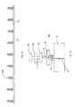
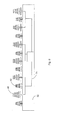
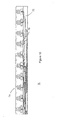
Figure 10 is Band 3 (or Band 4) antenna array fabricated on printed circuit board. - A multiband antenna, according to one example, includes a ground plane and a plurality of radiating elements. The ground plane may be a single sheet metal stamping.
- Referring to
Figure 1 , a first example, amultiband antenna 10 has four sets of radiating elements mounted on aground plane 12, A first set of radiatingelements 14 comprises a first linear array of microstrip annular ring elements 14a arranged on a longitudinal axis, approximately in the center of theground plane 12. The microstrip annular ring elements 14a are dimensioned to efficiently transmit and/or receive RF signals in Band 1. In this example, the first set of radiating elements comprises low band elements. The second set of radiatingelements 16 comprises a second linear array of crosseddipole elements dipole elements ground plane 12 on the longitudinal axis approximately in the center of theground plane 12. The crossed dipole elements are dimensioned for transmission and/or reception of RF signals, in Band 2. The crosseddipole elements 16a may be interspersed with the annular ring elements. Additionally, or alternately, the crosseddipole elements 16b may be nested within the microstrip annular ring elements. The cross dipole elements may be oriented so that the dipole elements are at approximately +45 degrees to vertical and -45 degrees to vertical to provide polarization diversity reception. The annular ring elements have two ±45 degree polarizations, and may be used to provide polarization diversity, also. - In another example, box dipole elements may be substituted for the crossed
dipole elements U.S. Patent 6,295,028 ). - A third set of radiating
elements 20 may comprise an array of radiatingelements 20a. In one example, thethird radiating elements 20a comprise directed dipole elements. These are commonly known as Yagi-Uda style radiating elements. The third set of radiatingelements 20 is located near the outer edge of theground plane 12. Referring toFigures 1 ,2a and 2b , in this example, the third set of radiatingelements 20 and the fourth set of radiatingelements 26 may be fabricated from sheet metal. The feed network may comprise airstrip conductors on one or both sides of theground plane 32. See, e.g.,Fig. 5 . A phase shifter (PCB or airstrip) may also be mounted on theground plane 12 and coupled to the airstrip feed lines as shown schematically inFig. 5 . An advantage of this example is that no additional supports are necessary for the directors, and the cost of the third and fourth sets of radiating elements is significantly reduced. Thethird radiating elements 20a are dimensioned for transmission and reception of RF signals in Band 3 or Band 4. - Referring to
Figure 2b , a close-up view of a radiating element according to one aspect of the present invention is provided. In this example,third radiating element 20a comprises a directed dipole, including adipole support 30 extending from aground plane 32, and adirector support 31 extending further from thedipole support 30.Director support 31 anddipole support 30 further include a 0.5wavelength balun slot 34.Dipole 36 is supported by thedipole support 30.Dipole 36 is perpendicular tobalun slot 34. Additionally,directors dipole 36 bydirector support 31. One end ofbalun slot 34 is near the beginning ofdirector 38a, and the other end is near the beginning ofground plane 32. Providingbalun slot 34 renders thedirector support 31 between thedipole 36 andfirst director 38a invisible with respect to RF signals. -
Airstrip line 40 is provided to excite theradiating element 20a.Airstrip line 40crosses balun slot 34 near the center ofbalun slot 34.Airstrip line 40 may be supported off theground plane 32 anddipole support 30 by plastic supports to provide an air dielectric. Theground plane 32,dipole support 30,director support 31,dipole 36, anddirectors ground plane 12. While other fabrication techniques may be used to construct directed dipoles of radiatingelement 20a, the stamped metal example has certain advantageous aspects. All of the components (dipole, directors, supports, ground plane) of many directed dipole elements may be fabricated as a single piece. This saves cost and assembly time. - A fourth set of radiating elements 26 (see
Figure 1 ) may comprise an array of directed dipole elements arranged along an edge of theground plane 12 opposite the third set of radiatingelements 20. Preferably, the fourth set of radiatingelements 26 are fabricated to be the same as the third set of radiatingelements 20. In this example, thefourth radiating elements 26a are directed dipole elements which are dimensioned to be the same as the third set of radiating elements, and the feed network is equivalent. For example, if the radiatingelements 20a of third set of radiatingelements 20 are dimensioned for transmission and/or reception of RF signals in Band 3, so are thefourth radiating elements 26a of the fourth set of radiatingelements 26. - In an alternate example (
Figure 10 ), the third and fourth sets of radiating elements are fabricated on a Printed Circuit Boards (PCB). A feed network may be fabricated on the PCB. The feed network may include variable elements, such as phase shifters, to adjust antenna radiation attributes, such as beam tilt. The feed network may also include a diplexer (e.g., between Band 1 and Band 3 or 4). - The distance between the third set of radiating
elements 20 and the fourth set of radiatingelements 26 may be in the range of 1.5 to 4 wavelengths of the Band 3 or Band 4 signals to allow for space diversity with correlation coefficient <0.5 and diversity gain >8dB. See, e.g., Compact Antenna Arrays for MIMO Application, IEEE AP-S 2001, v.3, pp. 708-11. See also, "Encyclopedia for RF and Microwave Engineering, editor Chang, Ky, 2005 (John Wiley & Sons, p. 332). A typical Base station dual-band antenna has a width of about 300mm. Accordingly, preferably, the third and fourth radiating elements are located near the outer edges of theground plane 12, to achieve a separation of about 2.2 wavelengths of Band 3. - With Yagi style directed dipole arrays separated by 2-4 wavelengths, 35-40 dB of inter-port isolation is achievable, which is well above the industry specification (>25-30dB) and a 10-15dub improvement over regular dipoles. The use of compact space diversity schemes has previously been limited by known regular dipoles. Use of Yagi style elements and vertical polarization (instead of 45 degree slant polarization, as is known) allows to achieve a F/B ratio improvement of 5dB to 1 0dB.
- The directed dipole arrangement of the example give above has been found to operate satisfactorily without causing undesirable levels of interference with the first and second sets of radiating elements (e.g., Band 1 and Band 2). Thanks to small electrical size of directed dipole for Band 1, 2. However, in another example, baffles may be included between the Band 1 and Band 2 elements and the Band 3 and/or Band 4 elements. Baffles may improve F/B and symmetry of the radiated pattern.
- By adjusting number of directors, azimuth beam width can be adjusted, matching with beam width of Band 1, Band 2. For example, a 65 degree beam requires 3-5 directors.
- In another aspect of this example, high directive Yagi style elements (with element pattern of∼60 degree in azimuth and ∼45 degree in elevation, which can be achieved with 5-6 directors) elements are used. The high directive elements allow an increase in spacing between elements (up to 1.2 wavelength) and reduces the number of elements required by 30% compared to regular dipole radiating elements. This provides a further cost savings.
- Referring to
Figures 3 and4 , in another example, the third and fourth sets of radiating elements may comprise Yagi-style directed elements with circular polarization.Elements Figure 4 that are the same as elements inFigure 1 receive the same reference characters, and the discussion of these elements is not repeated here. Referring toFigure 3 , a radiatingelement 44a is illustrated.Radiating element 44a comprises a directed dipole, including adipole support 50 extending from aground plane 52, and adirector support 51 extending further from thedipole support 50.Director support 51 anddipole support 50 further include a 0.5wavelength balun slot 54,Dipole 56 is supported by thedipole support 50.Dipole 56 is perpendicular tobalun slot 54. Additionally,directors dipole 56 bydirector support 51. - In this example, the
directors elements 44a, but are gradually rotated from a vertical position to a horizontal position, Additionally, thedirectors 58a-58e may be rotated to achieve orthogonal polarizations for the third and fourth sets of radiatingelements third radiating elements 44a may have thedirectors 58a-58e rotated to the right (clockwise), while thefourth radiating elements 46a may have the directors rotated to the left (counter clockwise). For 2.5-2.7 GHz (7% bandwidth), Left-Handed Circular Polarization and Right-Handed Circular Polarization is achievable with < 2dB axial ratio, as tests have shown. Electrically, these elements are relatively small compared to the Band 1 and Band 2 elements, and do not affect them. The circularly polarized elements may be constructed as elements fabricated from a metal stamping or in accordance with any other examples described herein, e.g., as PCBs or as a single stamping integral with theground plane 12. The combination of space diversity and polarization diversity leads to very low correlation and good diversity gain. Also, circular polarization is known for good in-building penetration and less mismatch with handsets. - In one example, each director is rotated at an angle Θ with respect to the immediately preceding director.
Director 58a, adjacent to thedipole 56, is rotated at an angle Θ with respect to thedipole 56. The angle Θ may be constant or variable. The angle Θ may be in the range of about 5 degrees to 25 degrees. One advantageous example, as illustrated inFigure 3 , illustrates that a circularly polarized directed-dipole element may be fabricated from a single sheet metal stamping. This is in contrast to conventional circular polarization schemes, which involves a quadrature coupler and two sets of orthogonal dipoles. - Referring to
Figure 5 , an assembly may include both Band 3radiating elements 60 and Band 4radiating elements 62. In this example, including both Band 3 and Band and Band 4radiating elements ground plane 12. Referring toFigure 5 , an example using directed dipole fabricated integrally with the ground plane is shown. In the illustrated example, themicrostrip feed network 64 for the Band 3 elements is shown, but, the microstrip feed network for the Band 4 elements is on the opposite side of theground plane 32 and is not shown. Diplexers may be integrated in to reduce the number of antenna connectors. - Referring to
Figure 10 , an example of a set of radiatingelements 70 suitable for Band 3 or Band 4 is illustrated using Printed Circuit Board (PCB) fabrication techniques. ThePCB 72 includes a plurality of directeddipoles 74, which are plated copper on a glass-reinforced plastic substrate. Also illustrated is afeed network 76 for the radiating elements disposed on the PCB. - The above examples provide the following benefits. There is polarization diversity in Band 1 and Band 2, and there is space diversity in Band 3 and/or Band 4. Additionally, in some examples, space diversity is coupled with polarization diversity in Band 3 and/or Band 4. Also, by providing separate feed networks, independent elevation in beam tilt is achieved for all three to four bands. There is the same (for example, 65 degree) azimuth beamwidth for all four bands, and acceptable front to back ratio for all four bands, due to Yagi style radiators for Band 3, 4, despite of their location on the very edge of the
ground plane 12. - In another example, illustrated in
multiband antenna 110 inFigure 6 , it may be desired to use conventional slant ±45 polarization for all bands without the use of Yagi-style directed dipoles. In one example of such asmultiband antenna 110, aground plane 112 and a plurality of radiating elements is provided. Theground plane 112 may comprise a center well 170 and a firstouter well 172 and a secondouter well 172. Theground plane 112 may be a single sheet metal stamping, or the center well 170 andouter wells 172 may be defined by walls or baffles. - Referring to
Figure 6 , one example of this embodiment having four sets of radiating elements is illustrated. A first set of radiatingelements 114 comprises a first linear array of firstpatch radiating elements 114a arranged on a longitudinal axis, approximately in the center of theground plane 112. The first patch elements are dimensioned to efficiently transmit and/or receive RF signals in Band 1. The second set of radiatingelements 116 comprises a second linear array ofsecond patch elements 116a. The second patch elements are also arranged in the center well 170 on the longitudinal axis approximately in the center of theground plane 112. The second patch elements are dimensioned for transmission and/or reception of RF signals, in Band 2. The second patch elements may be interspersed with the first patch elements. In alternate examples, the second patch elements may be nested within the first patch elements. - In another example, other types of dual polarized radiating elements can be used for Band 1 and 2; for example microstrip annular ring, box dipole, and/or crossed dipoles.
- A third set of radiating
elements 124 may comprise an array ofdipole radiating elements 124a, arranged at an angle of+45° to the longitudinal axis of theground plane 112, and disposed in the firstouter well 172. The third set of radiatingelements 124 are dimensioned for transmission and reception of RF signals in Band 3 or Band 4. - A fourth set of radiating
elements 126 may comprise an array ofdipole radiating elements 126a, arranged a -45°angle to the longitudinal axis of theground plane 112, and disposed in the secondouter well 172. The dipole elements of the fourth set of radiating elements are dimensioned to be the same as the dipole elements of the third set of radiating elements, only oriented so that the polarization is 90° to the third set of radiating elements. For example, if the dipole elements of third set of radiating elements are dimensioned for transmission and/or reception of RF signals in Band 3, so are the dipole elements of the fourth set of radiating elements. In this example, both polarization diversity (±45 degree) and space diversity (with spacing about 2.2 wavelength) are achieved for Band 3 (or Band 4), providing reduction of correlation coefficient and increasing of diversity gain. The use of the first and secondouter wells 172 enables the use of conventional dipole elements at 45 degree slants, without adversely affecting the performance of the Band 1 and Band 2 elements. - In the example of
Figure 6 , the firstouter well 172 and the second outer well 172 are approximately parallel with the center well 170. In an alternate example, illustrated. inFigure 7 , multiband antenna 2100 is illustrated. In this example,ground plane 212 is formed such that the first and secondouter wells 272 are angled inward with respect to center well 270. In this example, rotation of theouter wells 172 improves pattern squint of Band 3 and Band 4 and without degradation of Band 3 (4) radiation pattern due to edge effect. In particular,wells 172 are improving front-to-back and cross-polarization ratios for Band 3 (4). - In the examples described above, the radiating
elements 124a of the third set of radiatingelements 124 are disposed on one longitudinal axis, and the radiatingelements 126a of the fourth set of radiatingelements 126 are disposed on another longitudinal axis. In an alternate example, illustrated inFigure 8 ,multiband antenna 310 has a center well 370 andouter wells 372. Third set of radiatingelements 324 and fifth set of radiatingelements 344 are disposed in a firstouter well 372, while fourth set of radiatingelements 326 and sixth set of radiatingelements 346 are disposed in a secondouter well 372. In this example, the third and fourth sets of radiatingelements elements dipoles elements 324a may be staggered with respect to radiatingelements 344a, and radiatingelements 326a may be staggered with respect to radiatingelements 346a, so that they do not share a common axis, and/or may be offset from the center of theouter well 372. In an alternate embodiment, the multiband antenna may have only Band 3 or Band 4 elements, and the radiating elements within a set of radiating elements may be offset with respect to each other. This provides further improvement of beam stability and narrows azimuth beam width to 60-65°. - In another example (not illustrated), the third set of radiating elements comprises an array of box dipole elements disposed in the first outer well. The third set of radiating elements are dimensioned for efficient transmission and reception of RF signals in Band 3. The fourth set of radiating elements comprises an array of box dipole elements disposed in the second outer well. The fourth set of radiating elements are dimensioned for efficient transmission and reception of R.F signals in Band 4. In this example, a four-band 8-port antenna is realised. Alternatively, the third set of radiating elements and the fourth set of radiating elements need not be box dipole elements. In one example, the third set of radiating elements may comprise box dipole elements and the fourth set of radiating elements may comprise cross dipole elements. Other combinations of radiating elements are contemplated, including dipole of Band 3 crossed with dipole of Band 4.
- In another example, referring to
Figure 9 , third and forth sets of radiatingelements Fig. 9 ), or patch elements. Due to orthogonally of polarizations and physical separation between these 2 identical arrays, very low correlation coefficient between them is achieved, which benefits to LTE2.6 performance and using of 4x2 and 4x4 multiple-output (MIMO) schemes. Also, placing of 2 identical arrays for the same base station sector increases system capacity and throughput. - Although examples described above are related to wireless communications bands, the proposed solutions can be used for other bands and applications where multiband antennas are required.
Claims (26)
- A multiband antenna comprising:a longitudinal ground plane;a first set of first dual polarized radiating elements disposed lengthwise along a center of the ground plane, the first radiating elements being dimensioned to operate in a first frequency band;a second set of second dual polarized radiating elements disposed lengthwise along the center of the ground plane, the second radiating elements being dimensioned to operate in a second frequency band;a third set of third radiating elements disposed lengthwise on the ground plane on a first side of the first and second sets of radiating elements, the third radiating elements being dimensioned to operate at a third frequency band; anda fourth set of fourth radiating elements disposed lengthwise on the ground plane on a second side of the first and second sets of radiating elements, the fourth radiating elements being dimensioned to operate in the third frequency band,
- The multiband antenna of claim 1, wherein the first frequency band comprises about 790-960 MHz, the second frequency band comprises about 1710-2170 MHz, and the third frequency band comprises about 2.5 - 2.7 GHz.
- The multiband antenna of claim 1, wherein the first frequency band comprises about 790-960 MHz, the second frequency band comprises about 1710-2170 MHz, and the third frequency band comprises about 3.4 - 3. 8 GHz.
- The multiband antenna of claim 1, wherein the third and fourth radiating elements comprise directed dipole elements.
- The multiband antenna of claim 1, wherein the third and fourth radiating elements comprise circularly polarized directed dipole elements.
- The multiband antenna of claim 1, wherein the third and fourth radiating elements are disposed on a printed circuit board.
- The multiband antenna of claim 6, wherein the printed circuit board further includes a feed network.
- The multiband antenna of claim 1, wherein the third linear array of third radiating elements and the fourth linear array of fourth radiating elements are fabricated from sheet metal.
- The multiband antenna of claim 1, wherein the third and fourth radiating elements comprise a ground plane, a dipole support extending from the ground plane, a dipole supported by the dipole support, a director support extending from the dipole support, and a plurality of directors extending from the director support, wherein the ground plane, dipole support, dipole, director support, and directors are fabricated from a single piece of sheet metal.
- The multiband antenna of claim 9, further incorporating a 0.5 wavelength balun slot formed at least in part on the dipole support.
- The multi band antenna of claim 10, wherein each of the plurality of directors is rotated at an angle Θ with respect to its immediately preceding director, and a lower most director is rotated at an angle Θ with respect to the dipole.
- The multiband antenna of claim 9, wherein the third radiating elements are fabricated from a single piece of sheet metal to form the third set of radiating elements, and wherein the fourth radiating elements are fabricated from a single piece of sheet metal to form the fourth set of radiating elements.
- The multiband antenna of claim 1, wherein the third and fourth radiating elements comprise +/- 45 degree polarized elements.
- The multiband antenna of claim 1, wherein the longitudinal ground plane further comprises a center well and first and second outer wells, and wherein the first set of first radiating elements and the second set of second radiating elements are disposed in the center well, and third set of third radiating elements is disposed in the first outer well, and the fourth set of fourth radiating elements are disposed in the second outer well.
- The multiband antenna of claim 14, wherein the third and fourth radiating elements comprise +/- 45 degree polarized dipole elements.
- The multiband antenna of claim 1, further comprising a fifth set of fifth radiating elements interspersed with the third radiating elements, the fifth radiating elements being dimensioned to operate at a fourth frequency band; and
a sixth set of sixth radiating elements interspersed with the fourth radiating elements, the sixth radiating elements being dimensioned to operate in the fourth frequency band. - The multiband antenna of claim 16, wherein the first frequency band comprises about 790-960 MHz, the second frequency band comprises about 1710-2170 MHz, the third frequency band comprises about 2.5 - 2.7 GHz, and the fourth frequency band comprises about 3.4 - 3.8 GHz.
- A multiband antenna comprising:a longitudinal ground plane;a first set of first radiating elements disposed in a linear array along a center of the ground plane, the first radiating elements being dimensioned to operate in a first frequency band of about 790-960 MHz;a second set of second radiating elements disposed linear array along the center of the ground plane, the second radiating elements being dimensioned to operate in a second frequency band of about 1710-2170 MHz;a third set of third radiating elements disposed in a linear array on the ground plane on a first side of the first and second sets of radiating elements, the third radiating elements being directed dipole elements dimensioned to operate at a third frequency band; anda fourth set of fourth radiating elements disposed in a linear array on the ground plane on a second side of the first and second sets of radiating elements, the fourth radiating elements being directed dipole elements dimensioned to operate in the third frequency band.
- The multiband antenna of claim 18, wherein the third frequency band comprises about 2.5 - 2.7 GHz.
- The multiband antenna of claim 18, wherein the third frequency band comprises about 3.4 - 3.8 GHz.
- The multiband antenna of claim 18, further comprising a fifth set of fifth radiating elements interspersed with the third radiating elements, the fifth radiating elements being directed dipole elements dimensioned to operate at a fourth frequency band; and
a sixth set of sixth radiating elements interspersed with the fourth radiating elements, the sixth radiating elements being directed dipole elements dimensioned to operate in the fourth frequency band, wherein the third frequency band comprises about 2.5 - 2.7 GHz and the fourth frequency band comprises about 3.4 - 3.8 GHz. - A multiband antenna comprising:a longitudinal ground plane having a center well, a first outer well, and a second outer well;a first set of first radiating elements disposed lengthwise in the center well of the ground plane, the first radiating elements being dimensioned to operate in a first frequency band of about 790-960 MHz;a second set of second radiating elements disposed lengthwise in the center well of the ground plane, the second radiating elements being dimensioned to operate in a second frequency band of about 1710-2170 MHz;a third set of third radiating elements disposed lengthwise in the first outer well of the ground plane, the third radiating elements being dipole elements dimensioned to operate at a third frequency band and being oriented at +45 degrees to a longitudinal axis of the longitudinal ground plane; anda fourth set of fourth radiating elements disposed lengthwise in the second outer well of the ground plane, the fourth radiating elements being dipole elements dimensioned to operate at the third frequency band and being oriented at -45 degrees to a longitudinal axis of the longitudinal ground plane.
- The multiband antenna of claim 22, wherein the third frequency band comprises one of about 2.5 - 2.7 GHz and 3.8 GHz.
- The multiband antenna of claim 22, wherein the third set of radiating elements are not all disposed on a common lengthwise axis and the fourth set of radiating elements are not all disposed on a common lengthwise axis.
- The multiband antenna of claim 22, wherein the third radiating elements are dual polarized elements and the fourth radiating elements are dual polarized elements.
- The multiband antenna of claim 22, further comprising a fifth set of fifth radiating elements interspersed with the third radiating elements in the first outer well, the fifth radiating elements being dimensioned to operate at a fourth frequency band and being oriented at +45 degrees to a longitudinal axis of the ground plane; and
a sixth set of sixth dipole radiating elements interspersed with the fourth radiating elements in the second outer well, the sixth radiating elements being dimensioned to operate in the fourth frequency band and being oriented at -45 degrees to a longitudinal axis of the ground plane, wherein the third frequency band comprises about 2.5 - 2.7 GHz and the fourth frequency band comprises about 3.4 - 3.8 GHz.
Applications Claiming Priority (1)
| Application Number | Priority Date | Filing Date | Title |
|---|---|---|---|
| US13/099,550 US8674895B2 (en) | 2011-05-03 | 2011-05-03 | Multiband antenna |
Publications (2)
| Publication Number | Publication Date |
|---|---|
| EP2521222A1 true EP2521222A1 (en) | 2012-11-07 |
| EP2521222B1 EP2521222B1 (en) | 2017-07-12 |
Family
ID=46044529
Family Applications (1)
| Application Number | Title | Priority Date | Filing Date |
|---|---|---|---|
| EP12166519.4A Not-in-force EP2521222B1 (en) | 2011-05-03 | 2012-05-03 | Multiband antenna |
Country Status (4)
| Country | Link |
|---|---|
| US (1) | US8674895B2 (en) |
| EP (1) | EP2521222B1 (en) |
| CN (1) | CN102769174B (en) |
| BR (1) | BR102012010380A2 (en) |
Cited By (5)
| Publication number | Priority date | Publication date | Assignee | Title |
|---|---|---|---|---|
| CN104795635A (en) * | 2015-04-03 | 2015-07-22 | 京信通信技术(广州)有限公司 | Multifrequency array antenna |
| WO2016137757A1 (en) * | 2015-02-23 | 2016-09-01 | Qualcomm Incorporated | Antenna structures and configurations for millimeter wavelength wireless communications |
| WO2017176386A1 (en) | 2016-04-08 | 2017-10-12 | Commscope Technologies Llc | Ultra wide band radiators and related antenna arrays |
| CN109495984A (en) * | 2018-12-07 | 2019-03-19 | 苏州新海宜电子技术有限公司 | The intelligent self-organized network communication system and its working method of multichannel interactive information transmission |
| CN113823898A (en) * | 2021-07-22 | 2021-12-21 | 北京遥测技术研究所 | P/L/S three-frequency-band left-right-hand circularly polarized antenna array surface |
Families Citing this family (32)
| Publication number | Priority date | Publication date | Assignee | Title |
|---|---|---|---|---|
| EP2226890A1 (en) * | 2009-03-03 | 2010-09-08 | Hitachi Cable, Ltd. | Mobile communication base station antenna |
| US8692730B2 (en) * | 2009-03-03 | 2014-04-08 | Hitachi Metals, Ltd. | Mobile communication base station antenna |
| EP2706613B1 (en) * | 2012-09-11 | 2017-11-22 | Alcatel Lucent | Multi-band antenna with variable electrical tilt |
| CN102969575A (en) | 2012-11-30 | 2013-03-13 | 京信通信系统(中国)有限公司 | Multi-frequency array antenna |
| US9438278B2 (en) * | 2013-02-22 | 2016-09-06 | Quintel Technology Limited | Multi-array antenna |
| WO2014132254A1 (en) * | 2013-02-26 | 2014-09-04 | Galtronics Corporation Ltd. | Dual-polarized dipole antenna and cruciform coupling element therefore |
| CN105122542A (en) * | 2013-04-22 | 2015-12-02 | 盖尔创尼克斯有限公司 | Multiband antenna and slotted ground plane therefore |
| US9711871B2 (en) * | 2013-09-11 | 2017-07-18 | Commscope Technologies Llc | High-band radiators with extended-length feed stalks suitable for basestation antennas |
| US9444151B2 (en) | 2014-01-10 | 2016-09-13 | Commscope Technologies Llc | Enhanced phase shifter circuit to reduce RF cables |
| US10148012B2 (en) * | 2015-02-13 | 2018-12-04 | Commscope Technologies Llc | Base station antenna with dummy elements between subarrays |
| CN107210518A (en) * | 2015-02-25 | 2017-09-26 | 康普技术有限责任公司 | Full-wave doublet array with improved deflection performance |
| CN104733837A (en) * | 2015-03-20 | 2015-06-24 | 福建星网锐捷网络有限公司 | Antenna and antenna system |
| CN104882672A (en) * | 2015-05-28 | 2015-09-02 | 电子科技大学 | Wide bandwidth wave beam circular polarization Yagi-microstrip antenna |
| US10109917B2 (en) | 2015-09-30 | 2018-10-23 | Raytheon Company | Cupped antenna |
| US10790576B2 (en) * | 2015-12-14 | 2020-09-29 | Commscope Technologies Llc | Multi-band base station antennas having multi-layer feed boards |
| CN107275804B (en) | 2016-04-08 | 2022-03-04 | 康普技术有限责任公司 | Multiband Antenna Arrays with Common Mode Resonance (CMR) and Differential Mode Resonance (DMR) Removed |
| WO2018140305A1 (en) * | 2017-01-24 | 2018-08-02 | Commscope Technologies Llc | Base station antennas including supplemental arrays |
| EP3627622B1 (en) * | 2017-05-17 | 2022-08-24 | Tongyu Communication Inc. | Radiation element, as well as antenna unit and antenna array thereof |
| CN110870132B (en) | 2017-08-04 | 2021-09-07 | 华为技术有限公司 | Multiband Antenna |
| WO2019084232A1 (en) * | 2017-10-26 | 2019-05-02 | John Mezzalingua Associates, Llc D/B/A Jma Wireless | Low cost high performance multiband cellular antenna with cloaked monolithic metal dipole |
| WO2019113284A1 (en) * | 2017-12-06 | 2019-06-13 | Galtronics Usa, Inc. | Antenna array |
| US11043755B2 (en) | 2017-12-06 | 2021-06-22 | Galtronics Usa, Inc. | Antenna array |
| CN110858679B (en) * | 2018-08-24 | 2024-02-06 | 康普技术有限责任公司 | Multi-band base station antennas with broadband decoupled radiating elements and associated radiating elements |
| CN111129677B (en) * | 2018-10-31 | 2022-10-28 | 康普技术有限责任公司 | Isolator for antenna system and related antenna system |
| CN113826279B (en) * | 2019-03-29 | 2023-12-01 | 康普技术有限责任公司 | Dual-polarized dipole antenna with angled feed path that suppresses common-mode (monopole) radiation |
| US11251525B2 (en) * | 2019-06-11 | 2022-02-15 | Nokia Solutions And Networks Oy | Multi-band, dual-polarization antenna array |
| WO2021150365A1 (en) * | 2020-01-21 | 2021-07-29 | John Mezzalingua Associates, LLC | Multi-band antenna array face and radiator configuration for mitigating interference |
| CN114243258A (en) * | 2020-09-09 | 2022-03-25 | 康普技术有限责任公司 | Base station antenna comprising radiating elements with tilted dipoles |
| CN112768896B (en) * | 2020-12-29 | 2022-09-27 | 华南理工大学 | Antenna and communication device |
| CN116937123A (en) * | 2022-04-01 | 2023-10-24 | 康普技术有限责任公司 | Radiator assembly for a base station antenna |
| ES2975534B2 (en) * | 2023-06-19 | 2024-11-12 | Televes S A U | MULTIBAND YAGI ANTENNA |
| US12548906B2 (en) * | 2023-06-23 | 2026-02-10 | Qualcomm Incorporated | Patch antenna and dual-band interleaved array with passive element |
Citations (10)
| Publication number | Priority date | Publication date | Assignee | Title |
|---|---|---|---|---|
| US6295028B1 (en) | 1998-06-26 | 2001-09-25 | Allgon Ab | Dual band antenna |
| US6333720B1 (en) | 1998-05-27 | 2001-12-25 | Kathrein-Werke Ag | Dual polarized multi-range antenna |
| EP1227545A1 (en) * | 1999-10-26 | 2002-07-31 | Fractus, S.A. | Interlaced multiband antenna arrays |
| WO2003041289A1 (en) * | 2001-11-07 | 2003-05-15 | Ems Technologies, Inc. | Linearly-polarized dual-band base-station antenna |
| EP1353405A1 (en) * | 2002-04-10 | 2003-10-15 | Huber & Suhner Ag | Dual band antenna |
| US7173572B2 (en) * | 2002-02-28 | 2007-02-06 | Andrew Corporation | Dual band, dual pole, 90 degree azimuth BW, variable downtilt antenna |
| US7238101B2 (en) | 2004-05-20 | 2007-07-03 | Delphi Technologies, Inc. | Thermally conditioned vehicle seat |
| US7283101B2 (en) | 2003-06-26 | 2007-10-16 | Andrew Corporation | Antenna element, feed probe; dielectric spacer, antenna and method of communicating with a plurality of devices |
| US7405710B2 (en) | 2002-03-26 | 2008-07-29 | Andrew Corporation | Multiband dual polarized adjustable beamtilt base station antenna |
| WO2010063007A2 (en) * | 2008-11-26 | 2010-06-03 | Andrew Llc | Dual band base station antenna |
Family Cites Families (7)
| Publication number | Priority date | Publication date | Assignee | Title |
|---|---|---|---|---|
| US6765536B2 (en) * | 2002-05-09 | 2004-07-20 | Motorola, Inc. | Antenna with variably tuned parasitic element |
| US6924776B2 (en) * | 2003-07-03 | 2005-08-02 | Andrew Corporation | Wideband dual polarized base station antenna offering optimized horizontal beam radiation patterns and variable vertical beam tilt |
| CN101080848B (en) * | 2004-06-04 | 2012-09-12 | 安德鲁公司 | Directional Dipole Antenna |
| TWI318809B (en) * | 2005-05-23 | 2009-12-21 | Hon Hai Prec Ind Co Ltd | Multi-frequency antenna |
| US20100053008A1 (en) * | 2008-08-27 | 2010-03-04 | Pc-Tel, Inc. | Antenna having distributed phase shift mechanism |
| JP4916036B2 (en) * | 2010-02-23 | 2012-04-11 | カシオ計算機株式会社 | Multi-frequency antenna |
| US20120100817A1 (en) * | 2010-10-26 | 2012-04-26 | Motorola, Inc. | Loading of a twisted folded-monopole |
-
2011
- 2011-05-03 US US13/099,550 patent/US8674895B2/en active Active
-
2012
- 2012-05-02 BR BRBR102012010380-0A patent/BR102012010380A2/en not_active Application Discontinuation
- 2012-05-03 CN CN201210135500.7A patent/CN102769174B/en not_active Expired - Fee Related
- 2012-05-03 EP EP12166519.4A patent/EP2521222B1/en not_active Not-in-force
Patent Citations (10)
| Publication number | Priority date | Publication date | Assignee | Title |
|---|---|---|---|---|
| US6333720B1 (en) | 1998-05-27 | 2001-12-25 | Kathrein-Werke Ag | Dual polarized multi-range antenna |
| US6295028B1 (en) | 1998-06-26 | 2001-09-25 | Allgon Ab | Dual band antenna |
| EP1227545A1 (en) * | 1999-10-26 | 2002-07-31 | Fractus, S.A. | Interlaced multiband antenna arrays |
| WO2003041289A1 (en) * | 2001-11-07 | 2003-05-15 | Ems Technologies, Inc. | Linearly-polarized dual-band base-station antenna |
| US7173572B2 (en) * | 2002-02-28 | 2007-02-06 | Andrew Corporation | Dual band, dual pole, 90 degree azimuth BW, variable downtilt antenna |
| US7405710B2 (en) | 2002-03-26 | 2008-07-29 | Andrew Corporation | Multiband dual polarized adjustable beamtilt base station antenna |
| EP1353405A1 (en) * | 2002-04-10 | 2003-10-15 | Huber & Suhner Ag | Dual band antenna |
| US7283101B2 (en) | 2003-06-26 | 2007-10-16 | Andrew Corporation | Antenna element, feed probe; dielectric spacer, antenna and method of communicating with a plurality of devices |
| US7238101B2 (en) | 2004-05-20 | 2007-07-03 | Delphi Technologies, Inc. | Thermally conditioned vehicle seat |
| WO2010063007A2 (en) * | 2008-11-26 | 2010-06-03 | Andrew Llc | Dual band base station antenna |
Non-Patent Citations (2)
| Title |
|---|
| "Compact Antenna Arrays for MIMO Application", IEEE AP-S, vol. 3, 2001, pages 708 - 11 |
| "Encyclopedia for RF and Microwave Engineering", 2005, JOHN WILEY & SONS, pages: 332 |
Cited By (11)
| Publication number | Priority date | Publication date | Assignee | Title |
|---|---|---|---|---|
| WO2016137757A1 (en) * | 2015-02-23 | 2016-09-01 | Qualcomm Incorporated | Antenna structures and configurations for millimeter wavelength wireless communications |
| US9653818B2 (en) | 2015-02-23 | 2017-05-16 | Qualcomm Incorporated | Antenna structures and configurations for millimeter wavelength wireless communications |
| CN104795635A (en) * | 2015-04-03 | 2015-07-22 | 京信通信技术(广州)有限公司 | Multifrequency array antenna |
| CN104795635B (en) * | 2015-04-03 | 2017-11-28 | 京信通信技术(广州)有限公司 | Multi-frequency array antenna |
| WO2017176386A1 (en) | 2016-04-08 | 2017-10-12 | Commscope Technologies Llc | Ultra wide band radiators and related antenna arrays |
| EP3440741A4 (en) * | 2016-04-08 | 2019-12-11 | Commscope Technologies LLC | ULTRA-WIDE BAND RADIATING ELEMENTS AND ASSOCIATED ANTENNA ARRAYS |
| EP4187720A1 (en) * | 2016-04-08 | 2023-05-31 | CommScope Technologies LLC | Ultra wide band radiators and related antenna arrays |
| CN109495984A (en) * | 2018-12-07 | 2019-03-19 | 苏州新海宜电子技术有限公司 | The intelligent self-organized network communication system and its working method of multichannel interactive information transmission |
| CN109495984B (en) * | 2018-12-07 | 2020-01-07 | 苏州赛安电子技术有限公司 | Intelligent ad hoc network communication system for multi-channel interactive information transmission and its working method |
| CN113823898A (en) * | 2021-07-22 | 2021-12-21 | 北京遥测技术研究所 | P/L/S three-frequency-band left-right-hand circularly polarized antenna array surface |
| CN113823898B (en) * | 2021-07-22 | 2023-09-29 | 北京遥测技术研究所 | P/L/S three-frequency-band left-right circular polarization antenna array surface |
Also Published As
| Publication number | Publication date |
|---|---|
| CN102769174B (en) | 2016-09-21 |
| US8674895B2 (en) | 2014-03-18 |
| EP2521222B1 (en) | 2017-07-12 |
| US20120280878A1 (en) | 2012-11-08 |
| BR102012010380A2 (en) | 2015-08-11 |
| CN102769174A (en) | 2012-11-07 |
Similar Documents
| Publication | Publication Date | Title |
|---|---|---|
| EP2521222B1 (en) | Multiband antenna | |
| US11855352B2 (en) | Multi-band base station antennas having broadband decoupling radiating elements and related radiating elements | |
| US11196168B2 (en) | Ultra wide band radiators and related antennas arrays | |
| US9077070B2 (en) | Tri-pole antenna element and antenna array | |
| EP3619770B1 (en) | Multi-band base station antennas having crossed-dipole radiating elements | |
| US10903550B2 (en) | Base station antennas including supplemental arrays | |
| CN109863645B (en) | Ultra-wide bandwidth low-band radiating element | |
| US20040145526A1 (en) | Dual-band dual-polarized antenna array | |
| WO2014120062A1 (en) | An antenna arrangement and a base station | |
| CN105009361A (en) | An antenna arrangement and a base station | |
| US12597701B2 (en) | Base station antennas having f-style arrays that generate antenna beams having narrowed azimuth beamwidths | |
| US12620691B2 (en) | Base station antennas having radiating elements with active and/or cloaked directors for increased directivity | |
| US20250323426A1 (en) | Base station antennas with radiating elements having bent feed stalks and side feed | |
| US20250357660A1 (en) | Base station antennas with low-band arrays having low-band radiating elements having parasitic monopole elements | |
| EP4616485A1 (en) | Base station antennas having radiating elements with cloaked directors and/or multiple directors |
Legal Events
| Date | Code | Title | Description |
|---|---|---|---|
| PUAI | Public reference made under article 153(3) epc to a published international application that has entered the european phase |
Free format text: ORIGINAL CODE: 0009012 |
|
| AK | Designated contracting states |
Kind code of ref document: A1 Designated state(s): AL AT BE BG CH CY CZ DE DK EE ES FI FR GB GR HR HU IE IS IT LI LT LU LV MC MK MT NL NO PL PT RO RS SE SI SK SM TR |
|
| AX | Request for extension of the european patent |
Extension state: BA ME |
|
| 17P | Request for examination filed |
Effective date: 20130507 |
|
| RBV | Designated contracting states (corrected) |
Designated state(s): AL AT BE BG CH CY CZ DE DK EE ES FI FR GB GR HR HU IE IS IT LI LT LU LV MC MK MT NL NO PL PT RO RS SE SI SK SM TR |
|
| RAP1 | Party data changed (applicant data changed or rights of an application transferred) |
Owner name: COMMSCOPE TECHNOLOGIES LLC |
|
| 17Q | First examination report despatched |
Effective date: 20150630 |
|
| GRAP | Despatch of communication of intention to grant a patent |
Free format text: ORIGINAL CODE: EPIDOSNIGR1 |
|
| RIC1 | Information provided on ipc code assigned before grant |
Ipc: H01Q 5/00 20150101ALN20161125BHEP Ipc: H01Q 21/08 20060101AFI20161125BHEP Ipc: H01Q 21/30 20060101ALN20161125BHEP |
|
| RIC1 | Information provided on ipc code assigned before grant |
Ipc: H01Q 5/00 20150101ALN20161202BHEP Ipc: H01Q 21/08 20060101AFI20161202BHEP Ipc: H01Q 21/30 20060101ALN20161202BHEP |
|
| INTG | Intention to grant announced |
Effective date: 20161219 |
|
| GRAS | Grant fee paid |
Free format text: ORIGINAL CODE: EPIDOSNIGR3 |
|
| GRAA | (expected) grant |
Free format text: ORIGINAL CODE: 0009210 |
|
| AK | Designated contracting states |
Kind code of ref document: B1 Designated state(s): AL AT BE BG CH CY CZ DE DK EE ES FI FR GB GR HR HU IE IS IT LI LT LU LV MC MK MT NL NO PL PT RO RS SE SI SK SM TR |
|
| REG | Reference to a national code |
Ref country code: GB Ref legal event code: FG4D |
|
| REG | Reference to a national code |
Ref country code: CH Ref legal event code: EP |
|
| REG | Reference to a national code |
Ref country code: AT Ref legal event code: REF Ref document number: 909149 Country of ref document: AT Kind code of ref document: T Effective date: 20170715 |
|
| REG | Reference to a national code |
Ref country code: IE Ref legal event code: FG4D |
|
| REG | Reference to a national code |
Ref country code: DE Ref legal event code: R096 Ref document number: 602012034349 Country of ref document: DE |
|
| REG | Reference to a national code |
Ref country code: NL Ref legal event code: MP Effective date: 20170712 |
|
| REG | Reference to a national code |
Ref country code: LT Ref legal event code: MG4D |
|
| REG | Reference to a national code |
Ref country code: AT Ref legal event code: MK05 Ref document number: 909149 Country of ref document: AT Kind code of ref document: T Effective date: 20170712 |
|
| PG25 | Lapsed in a contracting state [announced via postgrant information from national office to epo] |
Ref country code: LT Free format text: LAPSE BECAUSE OF FAILURE TO SUBMIT A TRANSLATION OF THE DESCRIPTION OR TO PAY THE FEE WITHIN THE PRESCRIBED TIME-LIMIT Effective date: 20170712 Ref country code: SE Free format text: LAPSE BECAUSE OF FAILURE TO SUBMIT A TRANSLATION OF THE DESCRIPTION OR TO PAY THE FEE WITHIN THE PRESCRIBED TIME-LIMIT Effective date: 20170712 Ref country code: NO Free format text: LAPSE BECAUSE OF FAILURE TO SUBMIT A TRANSLATION OF THE DESCRIPTION OR TO PAY THE FEE WITHIN THE PRESCRIBED TIME-LIMIT Effective date: 20171012 Ref country code: NL Free format text: LAPSE BECAUSE OF FAILURE TO SUBMIT A TRANSLATION OF THE DESCRIPTION OR TO PAY THE FEE WITHIN THE PRESCRIBED TIME-LIMIT Effective date: 20170712 Ref country code: FI Free format text: LAPSE BECAUSE OF FAILURE TO SUBMIT A TRANSLATION OF THE DESCRIPTION OR TO PAY THE FEE WITHIN THE PRESCRIBED TIME-LIMIT Effective date: 20170712 Ref country code: AT Free format text: LAPSE BECAUSE OF FAILURE TO SUBMIT A TRANSLATION OF THE DESCRIPTION OR TO PAY THE FEE WITHIN THE PRESCRIBED TIME-LIMIT Effective date: 20170712 Ref country code: HR Free format text: LAPSE BECAUSE OF FAILURE TO SUBMIT A TRANSLATION OF THE DESCRIPTION OR TO PAY THE FEE WITHIN THE PRESCRIBED TIME-LIMIT Effective date: 20170712 |
|
| PG25 | Lapsed in a contracting state [announced via postgrant information from national office to epo] |
Ref country code: IS Free format text: LAPSE BECAUSE OF FAILURE TO SUBMIT A TRANSLATION OF THE DESCRIPTION OR TO PAY THE FEE WITHIN THE PRESCRIBED TIME-LIMIT Effective date: 20171112 Ref country code: BG Free format text: LAPSE BECAUSE OF FAILURE TO SUBMIT A TRANSLATION OF THE DESCRIPTION OR TO PAY THE FEE WITHIN THE PRESCRIBED TIME-LIMIT Effective date: 20171012 Ref country code: ES Free format text: LAPSE BECAUSE OF FAILURE TO SUBMIT A TRANSLATION OF THE DESCRIPTION OR TO PAY THE FEE WITHIN THE PRESCRIBED TIME-LIMIT Effective date: 20170712 Ref country code: LV Free format text: LAPSE BECAUSE OF FAILURE TO SUBMIT A TRANSLATION OF THE DESCRIPTION OR TO PAY THE FEE WITHIN THE PRESCRIBED TIME-LIMIT Effective date: 20170712 Ref country code: GR Free format text: LAPSE BECAUSE OF FAILURE TO SUBMIT A TRANSLATION OF THE DESCRIPTION OR TO PAY THE FEE WITHIN THE PRESCRIBED TIME-LIMIT Effective date: 20171013 Ref country code: RS Free format text: LAPSE BECAUSE OF FAILURE TO SUBMIT A TRANSLATION OF THE DESCRIPTION OR TO PAY THE FEE WITHIN THE PRESCRIBED TIME-LIMIT Effective date: 20170712 Ref country code: PL Free format text: LAPSE BECAUSE OF FAILURE TO SUBMIT A TRANSLATION OF THE DESCRIPTION OR TO PAY THE FEE WITHIN THE PRESCRIBED TIME-LIMIT Effective date: 20170712 |
|
| REG | Reference to a national code |
Ref country code: DE Ref legal event code: R097 Ref document number: 602012034349 Country of ref document: DE |
|
| PG25 | Lapsed in a contracting state [announced via postgrant information from national office to epo] |
Ref country code: CZ Free format text: LAPSE BECAUSE OF FAILURE TO SUBMIT A TRANSLATION OF THE DESCRIPTION OR TO PAY THE FEE WITHIN THE PRESCRIBED TIME-LIMIT Effective date: 20170712 Ref country code: DK Free format text: LAPSE BECAUSE OF FAILURE TO SUBMIT A TRANSLATION OF THE DESCRIPTION OR TO PAY THE FEE WITHIN THE PRESCRIBED TIME-LIMIT Effective date: 20170712 Ref country code: RO Free format text: LAPSE BECAUSE OF FAILURE TO SUBMIT A TRANSLATION OF THE DESCRIPTION OR TO PAY THE FEE WITHIN THE PRESCRIBED TIME-LIMIT Effective date: 20170712 |
|
| PLBE | No opposition filed within time limit |
Free format text: ORIGINAL CODE: 0009261 |
|
| STAA | Information on the status of an ep patent application or granted ep patent |
Free format text: STATUS: NO OPPOSITION FILED WITHIN TIME LIMIT |
|
| REG | Reference to a national code |
Ref country code: FR Ref legal event code: PLFP Year of fee payment: 7 |
|
| PG25 | Lapsed in a contracting state [announced via postgrant information from national office to epo] |
Ref country code: SK Free format text: LAPSE BECAUSE OF FAILURE TO SUBMIT A TRANSLATION OF THE DESCRIPTION OR TO PAY THE FEE WITHIN THE PRESCRIBED TIME-LIMIT Effective date: 20170712 Ref country code: IT Free format text: LAPSE BECAUSE OF FAILURE TO SUBMIT A TRANSLATION OF THE DESCRIPTION OR TO PAY THE FEE WITHIN THE PRESCRIBED TIME-LIMIT Effective date: 20170712 Ref country code: EE Free format text: LAPSE BECAUSE OF FAILURE TO SUBMIT A TRANSLATION OF THE DESCRIPTION OR TO PAY THE FEE WITHIN THE PRESCRIBED TIME-LIMIT Effective date: 20170712 Ref country code: SM Free format text: LAPSE BECAUSE OF FAILURE TO SUBMIT A TRANSLATION OF THE DESCRIPTION OR TO PAY THE FEE WITHIN THE PRESCRIBED TIME-LIMIT Effective date: 20170712 |
|
| 26N | No opposition filed |
Effective date: 20180413 |
|
| PG25 | Lapsed in a contracting state [announced via postgrant information from national office to epo] |
Ref country code: SI Free format text: LAPSE BECAUSE OF FAILURE TO SUBMIT A TRANSLATION OF THE DESCRIPTION OR TO PAY THE FEE WITHIN THE PRESCRIBED TIME-LIMIT Effective date: 20170712 |
|
| REG | Reference to a national code |
Ref country code: CH Ref legal event code: PL |
|
| REG | Reference to a national code |
Ref country code: BE Ref legal event code: MM Effective date: 20180531 |
|
| PG25 | Lapsed in a contracting state [announced via postgrant information from national office to epo] |
Ref country code: MC Free format text: LAPSE BECAUSE OF FAILURE TO SUBMIT A TRANSLATION OF THE DESCRIPTION OR TO PAY THE FEE WITHIN THE PRESCRIBED TIME-LIMIT Effective date: 20170712 |
|
| REG | Reference to a national code |
Ref country code: IE Ref legal event code: MM4A |
|
| PG25 | Lapsed in a contracting state [announced via postgrant information from national office to epo] |
Ref country code: LI Free format text: LAPSE BECAUSE OF NON-PAYMENT OF DUE FEES Effective date: 20180531 Ref country code: CH Free format text: LAPSE BECAUSE OF NON-PAYMENT OF DUE FEES Effective date: 20180531 |
|
| PG25 | Lapsed in a contracting state [announced via postgrant information from national office to epo] |
Ref country code: LU Free format text: LAPSE BECAUSE OF NON-PAYMENT OF DUE FEES Effective date: 20180503 |
|
| PG25 | Lapsed in a contracting state [announced via postgrant information from national office to epo] |
Ref country code: IE Free format text: LAPSE BECAUSE OF NON-PAYMENT OF DUE FEES Effective date: 20180503 |
|
| PG25 | Lapsed in a contracting state [announced via postgrant information from national office to epo] |
Ref country code: BE Free format text: LAPSE BECAUSE OF NON-PAYMENT OF DUE FEES Effective date: 20180531 |
|
| PG25 | Lapsed in a contracting state [announced via postgrant information from national office to epo] |
Ref country code: MT Free format text: LAPSE BECAUSE OF NON-PAYMENT OF DUE FEES Effective date: 20180503 |
|
| PG25 | Lapsed in a contracting state [announced via postgrant information from national office to epo] |
Ref country code: TR Free format text: LAPSE BECAUSE OF FAILURE TO SUBMIT A TRANSLATION OF THE DESCRIPTION OR TO PAY THE FEE WITHIN THE PRESCRIBED TIME-LIMIT Effective date: 20170712 |
|
| PG25 | Lapsed in a contracting state [announced via postgrant information from national office to epo] |
Ref country code: PT Free format text: LAPSE BECAUSE OF FAILURE TO SUBMIT A TRANSLATION OF THE DESCRIPTION OR TO PAY THE FEE WITHIN THE PRESCRIBED TIME-LIMIT Effective date: 20170712 Ref country code: HU Free format text: LAPSE BECAUSE OF FAILURE TO SUBMIT A TRANSLATION OF THE DESCRIPTION OR TO PAY THE FEE WITHIN THE PRESCRIBED TIME-LIMIT; INVALID AB INITIO Effective date: 20120503 |
|
| PG25 | Lapsed in a contracting state [announced via postgrant information from national office to epo] |
Ref country code: CY Free format text: LAPSE BECAUSE OF FAILURE TO SUBMIT A TRANSLATION OF THE DESCRIPTION OR TO PAY THE FEE WITHIN THE PRESCRIBED TIME-LIMIT Effective date: 20170712 Ref country code: MK Free format text: LAPSE BECAUSE OF NON-PAYMENT OF DUE FEES Effective date: 20170712 |
|
| PG25 | Lapsed in a contracting state [announced via postgrant information from national office to epo] |
Ref country code: AL Free format text: LAPSE BECAUSE OF FAILURE TO SUBMIT A TRANSLATION OF THE DESCRIPTION OR TO PAY THE FEE WITHIN THE PRESCRIBED TIME-LIMIT Effective date: 20170712 |
|
| PGFP | Annual fee paid to national office [announced via postgrant information from national office to epo] |
Ref country code: FR Payment date: 20210525 Year of fee payment: 10 Ref country code: DE Payment date: 20210527 Year of fee payment: 10 |
|
| PGFP | Annual fee paid to national office [announced via postgrant information from national office to epo] |
Ref country code: GB Payment date: 20210527 Year of fee payment: 10 |
|
| REG | Reference to a national code |
Ref country code: DE Ref legal event code: R119 Ref document number: 602012034349 Country of ref document: DE |
|
| GBPC | Gb: european patent ceased through non-payment of renewal fee |
Effective date: 20220503 |
|
| PG25 | Lapsed in a contracting state [announced via postgrant information from national office to epo] |
Ref country code: FR Free format text: LAPSE BECAUSE OF NON-PAYMENT OF DUE FEES Effective date: 20220531 |
|
| PG25 | Lapsed in a contracting state [announced via postgrant information from national office to epo] |
Ref country code: GB Free format text: LAPSE BECAUSE OF NON-PAYMENT OF DUE FEES Effective date: 20220503 Ref country code: DE Free format text: LAPSE BECAUSE OF NON-PAYMENT OF DUE FEES Effective date: 20221201 |