EP2521215A1 - Band-stop filter - Google Patents
Band-stop filter Download PDFInfo
- Publication number
- EP2521215A1 EP2521215A1 EP12158800A EP12158800A EP2521215A1 EP 2521215 A1 EP2521215 A1 EP 2521215A1 EP 12158800 A EP12158800 A EP 12158800A EP 12158800 A EP12158800 A EP 12158800A EP 2521215 A1 EP2521215 A1 EP 2521215A1
- Authority
- EP
- European Patent Office
- Prior art keywords
- filter
- rejection
- frequency
- channel
- band
- Prior art date
- Legal status (The legal status is an assumption and is not a legal conclusion. Google has not performed a legal analysis and makes no representation as to the accuracy of the status listed.)
- Granted
Links
- 230000005540 biological transmission Effects 0.000 claims abstract description 13
- 238000001914 filtration Methods 0.000 claims abstract description 13
- 230000008054 signal transmission Effects 0.000 claims abstract description 9
- 230000004044 response Effects 0.000 description 9
- 239000003990 capacitor Substances 0.000 description 8
- 238000004088 simulation Methods 0.000 description 5
- 239000000758 substrate Substances 0.000 description 5
- 230000008878 coupling Effects 0.000 description 4
- 238000010168 coupling process Methods 0.000 description 4
- 238000005859 coupling reaction Methods 0.000 description 4
- 238000010586 diagram Methods 0.000 description 4
- 238000005516 engineering process Methods 0.000 description 2
- 230000006872 improvement Effects 0.000 description 2
- 238000003780 insertion Methods 0.000 description 2
- 230000037431 insertion Effects 0.000 description 2
- 230000002452 interceptive effect Effects 0.000 description 2
- 230000015572 biosynthetic process Effects 0.000 description 1
- 230000008859 change Effects 0.000 description 1
- 230000010354 integration Effects 0.000 description 1
- 230000004048 modification Effects 0.000 description 1
- 238000012986 modification Methods 0.000 description 1
- 238000001228 spectrum Methods 0.000 description 1
- 238000003786 synthesis reaction Methods 0.000 description 1
Images

Classifications
-
- H—ELECTRICITY
- H01—ELECTRIC ELEMENTS
- H01P—WAVEGUIDES; RESONATORS, LINES, OR OTHER DEVICES OF THE WAVEGUIDE TYPE
- H01P1/00—Auxiliary devices
- H01P1/20—Frequency-selective devices, e.g. filters
-
- H—ELECTRICITY
- H01—ELECTRIC ELEMENTS
- H01P—WAVEGUIDES; RESONATORS, LINES, OR OTHER DEVICES OF THE WAVEGUIDE TYPE
- H01P1/00—Auxiliary devices
- H01P1/20—Frequency-selective devices, e.g. filters
- H01P1/201—Filters for transverse electromagnetic waves
- H01P1/203—Strip line filters
- H01P1/2039—Galvanic coupling between Input/Output
Definitions
- the present invention relates to an improvement to the band-rejection or band-stop filter, more specifically a band-rejection filter having simultaneously two rejection frequencies.
- the invention applies particularly in multi-standard multi-mode user terminals and in transmission and/or reception systems compliant with the standards DVB-H (Digital Video Broadcasting - Handheld) or DVB-T (Digital Video Broadcasting Terrestrial).
- Radio-communications systems that integrate several radio-communications systems are naturally subject to interferences due to the congestion of the frequencies spectrum by systems operating in frequency bands that are more and more close to each other or due to the size more and more reduced of these terminals, that means that the radio antennas used for transmission, particularly for radio-communications, are physically closer and closer creating as a result interference coupling that is harmful to the system.
- ultra selective filters are used, these filters making the systems immune to interferences.
- a filter input 1 and a filter output 2 a first signal transmission channel 3, called a direct channel, to which is coupled a second signal transmission channel 4, called a secondary channel.
- These two channels 3 and 4 are produced via transmission lines called micro-strip lines, as these lines are printed onto a substrate.
- the secondary path 4 forms a resonant line for which the length Ir is a function of ⁇ /2, giving a resonance frequency that corresponds to the frequency to signals to be rejected.
- the direct path 3 and the secondary path 4 are coupled together on a line length Is at the input 1 and the output 2 of the filter.
- the topology of the filter is defined so that, at the resonance frequency, the signal from the direct channel 3 and that from the secondary channel 4 combine in phase opposition at the filter output creating as a result an attenuation that is theoretically infinite in a band that is relatively narrow around the resonance frequency.
- a band-rejection filter as described above was simulated taking into consideration a micro-strip type line technology with the following parameters:
- This simulation shows, in particular, that there is obtained with this filter structure, a significant attenuation over a relatively wide frequency band. It can thus be deduced that the level of attenuation is not very sensitive to a variation in the phase difference between the main channel and the secondary channel.
- the present invention consists in using the properties of Guyette type band-rejection filters to produce a filter structure able to have simultaneously two band cut response types, namely two rejection frequencies , that is both compact and with little loss.
- the purpose of the present invention is thus a band-rejection filter comprising a filter input and a filter output,
- the filtering element is a low-pass filter for which the cut-off frequency is greater than the first rejection frequency of the filter.
- the low-pass filter is preferably constituted of at least two self-inductances in series on the secondary channel and at least one capacitor mounted between the self-inductances and a ground point, the value of self-inductances and the capacitor determining the cut-off frequency of the filter.
- the filtering element is a high-pass filter for which the cut-off frequency is less than the first rejection frequency of the filter.
- the high-pass filter is preferably constituted of at least two capacitors in series on the secondary channel and at least one self-inductance mounted between the capacitors and a ground point, the value of self-inductances and the value of capacitors determining the cut-off frequency of the filter.
- the first and/or second rejection frequencies can be modified by modifying the value of self-inductances and/or capacities of filtering elements.
- modifying the value of self-inductances and/or capacities of filtering elements can be modified by modifying the value of self-inductances and/or capacities of filtering elements.
- the band-rejection filter comprises a filter input 1 and a filter output 2. It also comprises a signal transmission channel 3 called a direct channel and a signal transmission channel 4 called a secondary channel. These two channels are located between the filter input 1 and the filter output 2.
- the channels 3 and 4 are produced by micro-strip lines printed on a dielectric substrate.
- the direct channel 3 and the secondary channel 4 are coupled together at the input and output of the filter.
- a part of the line 3' of the direct channel and a part of the line 4 of the secondary channel are arranged parallel to each other and close to one another in a way to create an electromagnetic coupling between the direct channel 3 and the secondary channel 4 at the input of the filter.
- a part of the line 3" of the direct channel 3 and a part of the line 4" of the secondary channel are arranged parallel to each other and close to one another in a way to create an electromagnetic coupling between the direct channel 3 and the secondary channel 4 at the output of the filter.
- the dimensions of line parts 4',3', 4", 3" are identical and the distance between said line parts at the input and at the output are the same so that the coupling is the same at the input and the output of the filter.
- the length of line elements constituting the direct channel 3 and the secondary channel 4 is determined so as to introduce at the rejection frequency a phase difference of 180° between the signal circulating via the direct channel 3 and the signal circulating via the secondary channel 4.
- the filtering element 5 that, in this embodiment, is constituted by a low-pass filter. More specifically and as shown in figure 3 , the low-pass filter 5 is constituted of two inductances or self-inductances 5a, 5b of value La mounted in series on the secondary channel 4 and a capacity 5c of value Ca mounted between the junction point of two inductances 5a, 5b and a ground point. It involves a low-pass filter of the order of 3 produced with discrete components. It is evident to those skilled in the art that the low-pass filter can also be produced using distributed technology such as transmission lines and/or that it can be of a higher order.
- the filter of figure 3 was simulated using as a substrate and as dimensions for the transmission lines, the elements used for the simulation of the filter of figure 1 . Moreover, the following parameters were taken into account:
- the curve shown represents the presence of two rejection frequencies, one around 730MHz and the other at around 1270MHz.
- the low-pass filter integrated at the secondary channel 4 introduces a positive phase difference that results in a shift in the resonance frequency of the initial filter shown in figure 1 .
- the initial frequency that was at around 1010MHz has passed to 730MHz, which corresponds to the first rejection frequency.
- the low-pass filter can be produced using for the capacity a varactor diode and for the self-inductance, an active inductance based on a transistor.
- a filtering element 6 constituted by a high-pass filter is integrated into the secondary channel 4. More specifically the high-pass filter 6 is formed from two capacitor elements 6a, 6b of value Ca mounted in series on the secondary channel and an inductor element or self-inductance 6c of value La mounted between the point of junction of two capacitor elements and a ground point.
- the high-pass filter 6 introduces a negative phase difference and its insertion into the secondary channel 4 offsets the resonance frequencies of the band-rejection filter to higher frequencies.
- figures 7A and 7B that show the response of the filter of figure 6 , it can be seen that the integration of a high-pass filter 6 in the secondary channel causes two resonance frequencies to appear namely, a first and a second rejection frequency.
- the self-inductance has a strong impedance and a minor variation of its value La does not change the conditions of this resonance, while at a low resonance frequency, the self inductance participates in the resonance circuit, that is checked by the value of the first rejection frequency that is located at 1.4 GHz in the case of figure 7A and at approximately 1.55 GHz in the case of figure 7B .
- the high pass filter 6a was described using discreet elements. However it is clear to those skilled in the art that the filter can also be produced using transmission line type elements.
- the high-pass filter described is a filter of the order 3. However, this filter can also be of a higher order.
Landscapes
- Physics & Mathematics (AREA)
- Electromagnetism (AREA)
- Control Of Motors That Do Not Use Commutators (AREA)
- Filters And Equalizers (AREA)
- Noise Elimination (AREA)
Abstract
- a filter input (1) and a filter output (2),
- a first signal transmission channel (3), called the direct channel, and a second signal transmission channel (4), called the secondary channel, located between said filter input and said filter output and coupled together at the filter input and the filter output, said direct channel and secondary channel each comprising at least one transmission line,
the secondary channel comprising a resonant element for which the resonance frequency is equal to a frequency to be rejected, called the first rejection frequency,
the direct channel and the secondary channel being designed to introduce at the rejection frequency a phase difference of 180° between the signal circulating via the direct channel and the signal circulating via the secondary channel,
the secondary channel (4) comprises in addition a filtering element (5) for which the cut-off frequency is different from said first rejection frequency in a way to create a second rejection frequency.
Description
- The present invention relates to an improvement to the band-rejection or band-stop filter, more specifically a band-rejection filter having simultaneously two rejection frequencies. The invention applies particularly in multi-standard multi-mode user terminals and in transmission and/or reception systems compliant with the standards DVB-H (Digital Video Broadcasting - Handheld) or DVB-T (Digital Video Broadcasting Terrestrial).
- User terminals that integrate several radio-communications systems are naturally subject to interferences due to the congestion of the frequencies spectrum by systems operating in frequency bands that are more and more close to each other or due to the size more and more reduced of these terminals, that means that the radio antennas used for transmission, particularly for radio-communications, are physically closer and closer creating as a result interference coupling that is harmful to the system. To overcome these disadvantages ultra selective filters are used, these filters making the systems immune to interferences.
- Thus, it has already been proposed in order to filter interference signals to use an appropriate band-rejection filter or a band-stop filter such as the filter discussed, for example, in the document titled "Exact Synthesis of Microwave Filters with Non-uniform Dissipation" by C. Guyette et al, IEEE-IMS-2007. Moreover, in the French patent application published under the number
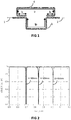
2947683 in the name of THOMSON Licensing figure 1 . It comprises between afilter input 1 and afilter output 2, a firstsignal transmission channel 3, called a direct channel, to which is coupled a secondsignal transmission channel 4, called a secondary channel. These twochannels secondary path 4 forms a resonant line for which the length Ir is a function of λ/2, giving a resonance frequency that corresponds to the frequency to signals to be rejected. Thedirect path 3 and thesecondary path 4 are coupled together on a line length Is at theinput 1 and theoutput 2 of the filter. The topology of the filter is defined so that, at the resonance frequency, the signal from thedirect channel 3 and that from thesecondary channel 4 combine in phase opposition at the filter output creating as a result an attenuation that is theoretically infinite in a band that is relatively narrow around the resonance frequency. This structure thus enables significant rejection levels to be obtained but at the cost of an increase in insertion losses, the level of losses depending on the quality factor of the resonating element. - A band-rejection filter as described above was simulated taking into consideration a micro-strip type line technology with the following parameters:
- The substrate selected is an Fr 4 substrate of thickness 0.25 mm and Er =4.5.
- The width of micro-strip line sis such that W = 0.44 mm to have a characteristic impedance of 50 ohms.
- The lines coupled on a length Is are selected such that s=100µm and Is=18.2 mm, s representing the distance between the two lines.
- The length of the
main line 3 = 2xIs + Ip, with Ip =72mm and the length of theresonant line 4 = 2*xIs+Ir. - In
figure 2 is shown the response in transmission of the filter for 3 values of Ir namely Ir=44 mm,60 mm and 80 mm. This simulation shows, in particular, that there is obtained with this filter structure, a significant attenuation over a relatively wide frequency band. It can thus be deduced that the level of attenuation is not very sensitive to a variation in the phase difference between the main channel and the secondary channel. - The present invention consists in using the properties of Guyette type band-rejection filters to produce a filter structure able to have simultaneously two band cut response types, namely two rejection frequencies , that is both compact and with little loss.
- The purpose of the present invention is thus a band-rejection filter comprising a filter input and a filter output,
- a first signal transmission channel, called the direct channel and a second transmission channel called the secondary channel arranged between said filter input and said filter output and coupled between them at the filter input and the filter output,
- said direct channel and said secondary channel each comprising at least one transmission line,
- the secondary channel comprising a resonant element for which the resonance frequency is equal to a frequency called the first rejection frequency,
- Thus is obtained with a single filter the possibility to simultaneously reject two interfering signals located close to a useful frequency band.
- According to a first embodiment, the filtering element is a low-pass filter for which the cut-off frequency is greater than the first rejection frequency of the filter. The low-pass filter is preferably constituted of at least two self-inductances in series on the secondary channel and at least one capacitor mounted between the self-inductances and a ground point, the value of self-inductances and the capacitor determining the cut-off frequency of the filter.
- According to a second embodiment, the filtering element is a high-pass filter for which the cut-off frequency is less than the first rejection frequency of the filter. The high-pass filter is preferably constituted of at least two capacitors in series on the secondary channel and at least one self-inductance mounted between the capacitors and a ground point, the value of self-inductances and the value of capacitors determining the cut-off frequency of the filter.
- According to another characteristic of the present invention, the first and/or second rejection frequencies can be modified by modifying the value of self-inductances and/or capacities of filtering elements. Thus it is possible to dynamically assign a rejection frequency without interfering with the other by working on one of the components of the filtering element. It is also possible to dynamically tune the two rejection frequencies at the same time by working on the values of different components of filtering elements.
- Other characteristics and advantages of the present invention will emerge upon reading the following description made with reference to the annexed drawings, wherein:
-
Figure 1 , already described, shows a structure of a band-rejection filter according to the prior art, -
Figure 2 , already described, shows a diagram showing the response of the filter offigure 1 for different resonant line lengths. -
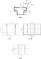
Figure 3 shows a first embodiment of a band-rejection filter with two rejection frequencies, according to the present invention. -
Figures 4a and 4b show a diagram giving the response in transmission of the filter offigure 3 for two different values of the capacity. -
Figure 5 shows a diagram giving the response of the filter offigure 3 for the value of different self-inductances. -
Figure 6 shows a second embodiment of a band-rejection filter with two rejection frequencies, according to the present invention. -
Figures 7A and 7b each show a diagram giving the response in transmission of the filter offigure 6 for two different values of the self-inductances.. - To simplify the description, in the figures, the same elements have the same references.
- A description will first be given, with reference to
figures 3 to 5 , of a first embodiment of band-rejection filter in accordance with the present invention. As shown infigure 3 , the band-rejection filter comprises afilter input 1 and afilter output 2. It also comprises asignal transmission channel 3 called a direct channel and asignal transmission channel 4 called a secondary channel. These two channels are located between thefilter input 1 and thefilter output 2. In the embodiment shown, thechannels figure 1 , thedirect channel 3 and thesecondary channel 4 are coupled together at the input and output of the filter. To do this, a part of the line 3' of the direct channel and a part of theline 4 of the secondary channel are arranged parallel to each other and close to one another in a way to create an electromagnetic coupling between thedirect channel 3 and thesecondary channel 4 at the input of the filter. Likewise, a part of theline 3" of thedirect channel 3 and a part of theline 4" of the secondary channel are arranged parallel to each other and close to one another in a way to create an electromagnetic coupling between thedirect channel 3 and thesecondary channel 4 at the output of the filter. In the example offigure 3 , the dimensions ofline parts 4',3', 4", 3" are identical and the distance between said line parts at the input and at the output are the same so that the coupling is the same at the input and the output of the filter. - The length of line elements constituting the
direct channel 3 and thesecondary channel 4 is determined so as to introduce at the rejection frequency a phase difference of 180° between the signal circulating via thedirect channel 3 and the signal circulating via thesecondary channel 4. - In accordance with the present invention, on the
secondary channel 4 is integrated afiltering element 5 that, in this embodiment, is constituted by a low-pass filter. More specifically and as shown infigure 3 , the low-pass filter 5 is constituted of two inductances or self-inductances secondary channel 4 and acapacity 5c of value Ca mounted between the junction point of twoinductances - The filter of
figure 3 was simulated using as a substrate and as dimensions for the transmission lines, the elements used for the simulation of the filter offigure 1 . Moreover, the following parameters were taken into account: - The simulation was made with a value Ir =44 mm. The two
inductances capacitor 5c has a value Ca = 4pF forfigure 4A and 6pF forfigure 4B . Moreover, an additional simulation was carried out with a self-inductance value of La=4nH and a capacity value Ca=6pF, the results of the simulation being given infigure 5 . - In
figure 4A , is shown the response of the filter for inductance values La=5nH and capacity Ca =4pF. The curve shown represents the presence of two rejection frequencies, one around 730MHz and the other at around 1270MHz. - If the curve of
figure 5 is compared with the curves offigure 2 , it can be seen that the low-pass filter integrated at thesecondary channel 4 introduces a positive phase difference that results in a shift in the resonance frequency of the initial filter shown infigure 1 . Thus the initial frequency that was at around 1010MHz has passed to 730MHz, which corresponds to the first rejection frequency. - Moreover, if the value Ca of the capacity is increased by 2 Pico farads, that is Ca= 6 picofarads,
figure 4B giving the response of the filter shows that the low resonance frequency remains unchanged though the high resonance frequency passes to approximately 1137MHz. In addition, if the inductance value La is modified to 4nH for a capacity Ca=6pF, it can be noted as shown infigure 5 that the two resonance frequencies, namely the first rejection frequency and the second rejection frequency, are both offset to high frequencies, the first rejection frequency being located at approximately 770MHz and the second rejection frequency being located at approximately 1190MHz. - Thus the filter structure shown in
figure 3 has the following advantages: - possibility to assign a single resonance frequency by variation only of the value Ca of the capacity,
- possibility to assign two resonance frequencies by modification of the values La and Ca of self-inductances and the capacity.
- In practice, to produce a dynamic assignment according to the interference situations that the multi-radio terminal must confront, the low-pass filter can be produced using for the capacity a varactor diode and for the self-inductance, an active inductance based on a transistor.
- A description will now be given, with reference to
figures 6, 7A and 7B of a second embodiment of a rejection filter in accordance with the present invention. As shown infigure 6 , the basic structure of the rejection filter is identical to the basic structure of the rejection filter offigure 3 . Consequently, the basic structure will not be described again hereafter. In accordance with the second embodiment of the present invention, afiltering element 6 constituted by a high-pass filter is integrated into thesecondary channel 4. More specifically the high-pass filter 6 is formed from twocapacitor elements 6a, 6b of value Ca mounted in series on the secondary channel and an inductor element or self-inductance 6c of value La mounted between the point of junction of two capacitor elements and a ground point. - The embodiment of
figure 6 was simulated by taking as a value of the basic structure the values of the rejection filter shown infigure 1 . Moreover, the secondary channel has a length Lr=44mm. The high-pass filter was simulated with capacity values Ca=11pF and for the self-inductance value La=4nH or La=2nH. - In this case, the high-
pass filter 6 introduces a negative phase difference and its insertion into thesecondary channel 4 offsets the resonance frequencies of the band-rejection filter to higher frequencies. As shown infigures 7A and 7B that show the response of the filter offigure 6 , it can be seen that the integration of a high-pass filter 6 in the secondary channel causes two resonance frequencies to appear namely, a first and a second rejection frequency. - As shown in
figures 7A and 7B , it can be seen that the variation of the value of the self-inductance from 4nH (Figure 7A ) to 2nH (Figure 7B ) does not cause variation in the second rejection frequency that remains constant at approximately 1.7GHz. - This can be explained by the fact that at the high resonance frequency, the self-inductance has a strong impedance and a minor variation of its value La does not change the conditions of this resonance, while at a low resonance frequency, the self inductance participates in the resonance circuit, that is checked by the value of the first rejection frequency that is located at 1.4 GHz in the case of
figure 7A and at approximately 1.55 GHz in the case offigure 7B . - In the embodiment of
figure 6 , the high pass filter 6a was described using discreet elements. However it is clear to those skilled in the art that the filter can also be produced using transmission line type elements. The high-pass filter described is a filter of theorder 3. However, this filter can also be of a higher order. - Though the invention has been described in relation to a specific embodiment, it is evident that this is in no way restricted and that it comprises all technical equivalents of the means described as well as their combinations if these enter into the scope of the invention.
characterized in that the secondary channel comprises in addition a filtering element for which the cut-off frequency is different from said first rejection frequency in a way to create a second rejection frequency.
Claims (8)
- Band-rejection filter comprising:- a filter input (1) and a filter output (2),- a first signal transmission channel (3), called the direct channel, and a second signal transmission channel (4), called the secondary channel, located between said filter input and said filter output and coupled together at the filter input and the filter output, said direct channel and secondary channel each comprising at least one transmission line,
the secondary channel comprising a resonant element for which the resonance frequency is equal to a frequency to be rejected, called the first rejection frequency,
the direct channel and the secondary channel being designed to introduce at the rejection frequency a phase difference of 180° between the signal circulating via the direct channel and the signal circulating via the secondary channel,
characterized in that the secondary channel (4) comprises in addition a filtering element (5,6) for which the cut-off frequency is different from said first rejection frequency in a way to create a second rejection frequency distinct from said first rejection frequency. - Band-rejection filter according to claim 1, characterized in that the filtering element is a low-pass filter for which the cut-off frequency is greater than the first rejection frequency of the filter.
- Band-rejection filter according to claim 2, characterized in that the low-pass filter is constituted by at least two self-inductances (5a, 5b) in series on the secondary channel and at least one capacity (5c) mounted between self-inductances and a ground point, the value of self-inductances and capacity determining the cut-off frequency of the filter.
- Band-rejection filter according to claim 1, characterized in that the filtering element is a high-pass filter for which the cut-off frequency is less than the first rejection frequency of the filter.
- Band-rejection filter according to claim 4, characterized in that the high-pass filter is constituted by at least two capacities (6a, 6b) in series on the secondary channel and at least one self-inductance (6c) mounted between capacities and a ground point, the value of self-inductances and capacity determining the cut-off frequency of the filter.
- Band-rejection filter according to claim 3 or claim 5, characterized in that the first and/or second rejection frequencies can be modified by modifying the value of self-inductances and/or capacities of filtering elements.
- Band-rejection filter according to any one of claims 1 to 6, characterized in that the resonant element of the secondary channel is constituted by a resonant line of length λ/2, λ being the wavelength of the resonance frequency.
- Multi-standard multi-mode terminal, characterized in that it comprises a band-rejection filter according to any one of claims 1 to 7.
Applications Claiming Priority (1)
| Application Number | Priority Date | Filing Date | Title |
|---|---|---|---|
| FR1153855A FR2974958A1 (en) | 2011-05-05 | 2011-05-05 | STOP BAND FILTER |
Publications (2)
| Publication Number | Publication Date |
|---|---|
| EP2521215A1 true EP2521215A1 (en) | 2012-11-07 |
| EP2521215B1 EP2521215B1 (en) | 2013-11-13 |
Family
ID=45787137
Family Applications (1)
| Application Number | Title | Priority Date | Filing Date |
|---|---|---|---|
| EP12158800.8A Not-in-force EP2521215B1 (en) | 2011-05-05 | 2012-03-09 | Band-stop filter |
Country Status (5)
| Country | Link |
|---|---|
| US (1) | US20120284766A1 (en) |
| EP (1) | EP2521215B1 (en) |
| JP (1) | JP5940880B2 (en) |
| CN (1) | CN102769159A (en) |
| FR (1) | FR2974958A1 (en) |
Families Citing this family (2)
| Publication number | Priority date | Publication date | Assignee | Title |
|---|---|---|---|---|
| CN104183913B (en) * | 2014-08-18 | 2017-10-31 | 浙江大学 | Broadband circle polarized RFID handheld readers antenna |
| CN114826187A (en) * | 2022-03-29 | 2022-07-29 | 清华大学 | Filter and electronic device |
Citations (2)
| Publication number | Priority date | Publication date | Assignee | Title |
|---|---|---|---|---|
| US20060273869A1 (en) * | 2005-06-06 | 2006-12-07 | Jachowski Douglas R | Narrow-band absorptive bandstop filter with multiple signal paths |
| EP2251927A1 (en) * | 2009-05-14 | 2010-11-17 | Thomson Licensing | Dual-response stopband filter |
Family Cites Families (11)
| Publication number | Priority date | Publication date | Assignee | Title |
|---|---|---|---|---|
| US3480884A (en) * | 1968-08-26 | 1969-11-25 | Hewlett Packard Co | Electromagnetic wave energy coupling apparatus comprising an anisotropic dielectric slab |
| US4290517A (en) * | 1978-11-29 | 1981-09-22 | Owens-Illinois, Inc. | Method and apparatus for reducing loader bar impact |
| US6621370B1 (en) * | 2000-09-15 | 2003-09-16 | Atheros Communications, Inc. | Method and system for a lumped-distributed balun |
| US6636128B2 (en) * | 2001-06-07 | 2003-10-21 | The United States Of America As Represented By The Secretary Of The Navy | Frequency-tunable notch filter |
| US7057472B2 (en) * | 2001-08-10 | 2006-06-06 | Hitachi Metals, Ltd. | Bypass filter, multi-band antenna switch circuit, and layered module composite part and communication device using them |
| JP4241400B2 (en) * | 2004-01-09 | 2009-03-18 | 株式会社豊田中央研究所 | Balanced line-unbalanced line connector |
| US7012484B2 (en) * | 2004-04-26 | 2006-03-14 | Integrated System Solution Corp. | Filter using multilayer ceramic technology and structure thereof |
| US8289103B2 (en) * | 2006-11-20 | 2012-10-16 | Panasonic Corporation | Filter device having attenuation poles |
| US8576133B2 (en) * | 2007-06-22 | 2013-11-05 | Broadcom Corporation | Adjustable antenna assembly for receive blocking |
| CN201185407Y (en) * | 2008-04-24 | 2009-01-21 | 顺泰电子科技股份有限公司 | notch filter |
| US8487717B2 (en) * | 2010-02-01 | 2013-07-16 | Ppc Broadband, Inc. | Multipath mitigation circuit for home network |
-
2011
- 2011-05-05 FR FR1153855A patent/FR2974958A1/en not_active Withdrawn
-
2012
- 2012-03-09 EP EP12158800.8A patent/EP2521215B1/en not_active Not-in-force
- 2012-04-17 CN CN2012101124661A patent/CN102769159A/en active Pending
- 2012-04-30 US US13/459,656 patent/US20120284766A1/en not_active Abandoned
- 2012-05-07 JP JP2012106085A patent/JP5940880B2/en not_active Expired - Fee Related
Patent Citations (2)
| Publication number | Priority date | Publication date | Assignee | Title |
|---|---|---|---|---|
| US20060273869A1 (en) * | 2005-06-06 | 2006-12-07 | Jachowski Douglas R | Narrow-band absorptive bandstop filter with multiple signal paths |
| EP2251927A1 (en) * | 2009-05-14 | 2010-11-17 | Thomson Licensing | Dual-response stopband filter |
Non-Patent Citations (1)
| Title |
|---|
| C. GUYETTE ET AL.: "Exact Synthesis of Microwave Filters with Non-uniform Dissipation", IEEE-IMS-2007, 2007 |
Also Published As
| Publication number | Publication date |
|---|---|
| EP2521215B1 (en) | 2013-11-13 |
| CN102769159A (en) | 2012-11-07 |
| US20120284766A1 (en) | 2012-11-08 |
| FR2974958A1 (en) | 2012-11-09 |
| JP5940880B2 (en) | 2016-06-29 |
| JP2013042477A (en) | 2013-02-28 |
Similar Documents
| Publication | Publication Date | Title |
|---|---|---|
| US10340874B2 (en) | Filter circuit, RF front end circuit, and communication apparatus | |
| SG182406A1 (en) | Antenna and receiver circuit | |
| US9203375B2 (en) | Band rejection filter comprising a serial connection of at least two pi-elements | |
| US20160181678A1 (en) | Band-rejection filter | |
| US9979375B2 (en) | Multi-harmonic matching networks | |
| US20180034125A1 (en) | Waveguide E-Plane Filter | |
| US9413328B2 (en) | Diplexer including two bandpass filters | |
| US10547337B2 (en) | Radio frequency front-end circuit and communication device | |
| US20140340174A1 (en) | Active filter with dual response | |
| EP2521215B1 (en) | Band-stop filter | |
| US10903812B2 (en) | Trap filter and filter circuit | |
| KR101391399B1 (en) | Band Stop Filter of Composite Right/Left Handed Structure and the Manufacturing Method thereof | |
| US10581132B2 (en) | Tuneable band pass filter | |
| US10454148B2 (en) | Compact band pass filter | |
| US7573355B2 (en) | Integrated bandpass/bandstop coupled line filter | |
| CN112335177B (en) | Multiplexer | |
| US20110291773A1 (en) | Dual-response stopband filter | |
| KR20120125191A (en) | Band-stop filter | |
| US20190372545A1 (en) | Compact band pass filter with vias | |
| Borhani et al. | Quad notched-band UWB BPF based on quintuple-mode resonator | |
| KR101482954B1 (en) | LC diplexer and access point apparatus | |
| US20260005664A1 (en) | Filter circuit, diplexer, radio-frequency front-end circuit, and communication device | |
| US9520632B2 (en) | CMOS band-pass filter | |
| Lababidi et al. | Tunable semi-lumped dual response filter using active capacitor circuit for multistandard systems | |
| JP2008270973A (en) | Television signal input circuit |
Legal Events
| Date | Code | Title | Description |
|---|---|---|---|
| PUAI | Public reference made under article 153(3) epc to a published international application that has entered the european phase |
Free format text: ORIGINAL CODE: 0009012 |
|
| AK | Designated contracting states |
Kind code of ref document: A1 Designated state(s): AL AT BE BG CH CY CZ DE DK EE ES FI FR GB GR HR HU IE IS IT LI LT LU LV MC MK MT NL NO PL PT RO RS SE SI SK SM TR |
|
| AX | Request for extension of the european patent |
Extension state: BA ME |
|
| 17P | Request for examination filed |
Effective date: 20130426 |
|
| GRAP | Despatch of communication of intention to grant a patent |
Free format text: ORIGINAL CODE: EPIDOSNIGR1 |
|
| RIC1 | Information provided on ipc code assigned before grant |
Ipc: H01P 1/20 20060101AFI20130531BHEP |
|
| INTG | Intention to grant announced |
Effective date: 20130702 |
|
| GRAS | Grant fee paid |
Free format text: ORIGINAL CODE: EPIDOSNIGR3 |
|
| GRAA | (expected) grant |
Free format text: ORIGINAL CODE: 0009210 |
|
| AK | Designated contracting states |
Kind code of ref document: B1 Designated state(s): AL AT BE BG CH CY CZ DE DK EE ES FI FR GB GR HR HU IE IS IT LI LT LU LV MC MK MT NL NO PL PT RO RS SE SI SK SM TR |
|
| REG | Reference to a national code |
Ref country code: GB Ref legal event code: FG4D |
|
| REG | Reference to a national code |
Ref country code: CH Ref legal event code: EP |
|
| REG | Reference to a national code |
Ref country code: AT Ref legal event code: REF Ref document number: 640924 Country of ref document: AT Kind code of ref document: T Effective date: 20131215 |
|
| REG | Reference to a national code |
Ref country code: IE Ref legal event code: FG4D |
|
| REG | Reference to a national code |
Ref country code: DE Ref legal event code: R096 Ref document number: 602012000468 Country of ref document: DE Effective date: 20140109 |
|
| REG | Reference to a national code |
Ref country code: DE Ref legal event code: R084 Ref document number: 602012000468 Country of ref document: DE Effective date: 20131116 |
|
| REG | Reference to a national code |
Ref country code: NL Ref legal event code: VDEP Effective date: 20131113 |
|
| REG | Reference to a national code |
Ref country code: AT Ref legal event code: MK05 Ref document number: 640924 Country of ref document: AT Kind code of ref document: T Effective date: 20131113 |
|
| REG | Reference to a national code |
Ref country code: LT Ref legal event code: MG4D |
|
| PG25 | Lapsed in a contracting state [announced via postgrant information from national office to epo] |
Ref country code: LT Free format text: LAPSE BECAUSE OF FAILURE TO SUBMIT A TRANSLATION OF THE DESCRIPTION OR TO PAY THE FEE WITHIN THE PRESCRIBED TIME-LIMIT Effective date: 20131113 Ref country code: HR Free format text: LAPSE BECAUSE OF FAILURE TO SUBMIT A TRANSLATION OF THE DESCRIPTION OR TO PAY THE FEE WITHIN THE PRESCRIBED TIME-LIMIT Effective date: 20131113 Ref country code: NL Free format text: LAPSE BECAUSE OF FAILURE TO SUBMIT A TRANSLATION OF THE DESCRIPTION OR TO PAY THE FEE WITHIN THE PRESCRIBED TIME-LIMIT Effective date: 20131113 Ref country code: FI Free format text: LAPSE BECAUSE OF FAILURE TO SUBMIT A TRANSLATION OF THE DESCRIPTION OR TO PAY THE FEE WITHIN THE PRESCRIBED TIME-LIMIT Effective date: 20131113 Ref country code: NO Free format text: LAPSE BECAUSE OF FAILURE TO SUBMIT A TRANSLATION OF THE DESCRIPTION OR TO PAY THE FEE WITHIN THE PRESCRIBED TIME-LIMIT Effective date: 20140213 Ref country code: SE Free format text: LAPSE BECAUSE OF FAILURE TO SUBMIT A TRANSLATION OF THE DESCRIPTION OR TO PAY THE FEE WITHIN THE PRESCRIBED TIME-LIMIT Effective date: 20131113 Ref country code: IS Free format text: LAPSE BECAUSE OF FAILURE TO SUBMIT A TRANSLATION OF THE DESCRIPTION OR TO PAY THE FEE WITHIN THE PRESCRIBED TIME-LIMIT Effective date: 20140313 |
|
| PG25 | Lapsed in a contracting state [announced via postgrant information from national office to epo] |
Ref country code: RS Free format text: LAPSE BECAUSE OF FAILURE TO SUBMIT A TRANSLATION OF THE DESCRIPTION OR TO PAY THE FEE WITHIN THE PRESCRIBED TIME-LIMIT Effective date: 20131113 Ref country code: CY Free format text: LAPSE BECAUSE OF FAILURE TO SUBMIT A TRANSLATION OF THE DESCRIPTION OR TO PAY THE FEE WITHIN THE PRESCRIBED TIME-LIMIT Effective date: 20131113 Ref country code: ES Free format text: LAPSE BECAUSE OF FAILURE TO SUBMIT A TRANSLATION OF THE DESCRIPTION OR TO PAY THE FEE WITHIN THE PRESCRIBED TIME-LIMIT Effective date: 20131113 Ref country code: LV Free format text: LAPSE BECAUSE OF FAILURE TO SUBMIT A TRANSLATION OF THE DESCRIPTION OR TO PAY THE FEE WITHIN THE PRESCRIBED TIME-LIMIT Effective date: 20131113 Ref country code: BE Free format text: LAPSE BECAUSE OF FAILURE TO SUBMIT A TRANSLATION OF THE DESCRIPTION OR TO PAY THE FEE WITHIN THE PRESCRIBED TIME-LIMIT Effective date: 20131113 Ref country code: AT Free format text: LAPSE BECAUSE OF FAILURE TO SUBMIT A TRANSLATION OF THE DESCRIPTION OR TO PAY THE FEE WITHIN THE PRESCRIBED TIME-LIMIT Effective date: 20131113 |
|
| PG25 | Lapsed in a contracting state [announced via postgrant information from national office to epo] |
Ref country code: PT Free format text: LAPSE BECAUSE OF FAILURE TO SUBMIT A TRANSLATION OF THE DESCRIPTION OR TO PAY THE FEE WITHIN THE PRESCRIBED TIME-LIMIT Effective date: 20140313 |
|
| PG25 | Lapsed in a contracting state [announced via postgrant information from national office to epo] |
Ref country code: EE Free format text: LAPSE BECAUSE OF FAILURE TO SUBMIT A TRANSLATION OF THE DESCRIPTION OR TO PAY THE FEE WITHIN THE PRESCRIBED TIME-LIMIT Effective date: 20131113 |
|
| REG | Reference to a national code |
Ref country code: DE Ref legal event code: R097 Ref document number: 602012000468 Country of ref document: DE |
|
| PG25 | Lapsed in a contracting state [announced via postgrant information from national office to epo] |
Ref country code: PL Free format text: LAPSE BECAUSE OF FAILURE TO SUBMIT A TRANSLATION OF THE DESCRIPTION OR TO PAY THE FEE WITHIN THE PRESCRIBED TIME-LIMIT Effective date: 20131113 Ref country code: SK Free format text: LAPSE BECAUSE OF FAILURE TO SUBMIT A TRANSLATION OF THE DESCRIPTION OR TO PAY THE FEE WITHIN THE PRESCRIBED TIME-LIMIT Effective date: 20131113 Ref country code: CZ Free format text: LAPSE BECAUSE OF FAILURE TO SUBMIT A TRANSLATION OF THE DESCRIPTION OR TO PAY THE FEE WITHIN THE PRESCRIBED TIME-LIMIT Effective date: 20131113 |
|
| PLBE | No opposition filed within time limit |
Free format text: ORIGINAL CODE: 0009261 |
|
| STAA | Information on the status of an ep patent application or granted ep patent |
Free format text: STATUS: NO OPPOSITION FILED WITHIN TIME LIMIT |
|
| PG25 | Lapsed in a contracting state [announced via postgrant information from national office to epo] |
Ref country code: DK Free format text: LAPSE BECAUSE OF FAILURE TO SUBMIT A TRANSLATION OF THE DESCRIPTION OR TO PAY THE FEE WITHIN THE PRESCRIBED TIME-LIMIT Effective date: 20131113 |
|
| 26N | No opposition filed |
Effective date: 20140814 |
|
| PG25 | Lapsed in a contracting state [announced via postgrant information from national office to epo] |
Ref country code: LU Free format text: LAPSE BECAUSE OF FAILURE TO SUBMIT A TRANSLATION OF THE DESCRIPTION OR TO PAY THE FEE WITHIN THE PRESCRIBED TIME-LIMIT Effective date: 20140309 |
|
| REG | Reference to a national code |
Ref country code: DE Ref legal event code: R097 Ref document number: 602012000468 Country of ref document: DE Effective date: 20140814 |
|
| REG | Reference to a national code |
Ref country code: IE Ref legal event code: MM4A |
|
| PG25 | Lapsed in a contracting state [announced via postgrant information from national office to epo] |
Ref country code: IE Free format text: LAPSE BECAUSE OF NON-PAYMENT OF DUE FEES Effective date: 20140309 |
|
| PG25 | Lapsed in a contracting state [announced via postgrant information from national office to epo] |
Ref country code: SI Free format text: LAPSE BECAUSE OF FAILURE TO SUBMIT A TRANSLATION OF THE DESCRIPTION OR TO PAY THE FEE WITHIN THE PRESCRIBED TIME-LIMIT Effective date: 20131113 |
|
| PG25 | Lapsed in a contracting state [announced via postgrant information from national office to epo] |
Ref country code: IT Free format text: LAPSE BECAUSE OF FAILURE TO SUBMIT A TRANSLATION OF THE DESCRIPTION OR TO PAY THE FEE WITHIN THE PRESCRIBED TIME-LIMIT Effective date: 20131113 |
|
| REG | Reference to a national code |
Ref country code: CH Ref legal event code: PL |
|
| PG25 | Lapsed in a contracting state [announced via postgrant information from national office to epo] |
Ref country code: LI Free format text: LAPSE BECAUSE OF NON-PAYMENT OF DUE FEES Effective date: 20150331 Ref country code: CH Free format text: LAPSE BECAUSE OF NON-PAYMENT OF DUE FEES Effective date: 20150331 |
|
| PG25 | Lapsed in a contracting state [announced via postgrant information from national office to epo] |
Ref country code: MT Free format text: LAPSE BECAUSE OF FAILURE TO SUBMIT A TRANSLATION OF THE DESCRIPTION OR TO PAY THE FEE WITHIN THE PRESCRIBED TIME-LIMIT Effective date: 20131113 |
|
| REG | Reference to a national code |
Ref country code: FR Ref legal event code: PLFP Year of fee payment: 5 |
|
| PG25 | Lapsed in a contracting state [announced via postgrant information from national office to epo] |
Ref country code: SM Free format text: LAPSE BECAUSE OF FAILURE TO SUBMIT A TRANSLATION OF THE DESCRIPTION OR TO PAY THE FEE WITHIN THE PRESCRIBED TIME-LIMIT Effective date: 20131113 |
|
| PGFP | Annual fee paid to national office [announced via postgrant information from national office to epo] |
Ref country code: DE Payment date: 20160324 Year of fee payment: 5 |
|
| PG25 | Lapsed in a contracting state [announced via postgrant information from national office to epo] |
Ref country code: RO Free format text: LAPSE BECAUSE OF FAILURE TO SUBMIT A TRANSLATION OF THE DESCRIPTION OR TO PAY THE FEE WITHIN THE PRESCRIBED TIME-LIMIT Effective date: 20131113 Ref country code: MC Free format text: LAPSE BECAUSE OF FAILURE TO SUBMIT A TRANSLATION OF THE DESCRIPTION OR TO PAY THE FEE WITHIN THE PRESCRIBED TIME-LIMIT Effective date: 20131113 |
|
| PGFP | Annual fee paid to national office [announced via postgrant information from national office to epo] |
Ref country code: FR Payment date: 20160324 Year of fee payment: 5 |
|
| PG25 | Lapsed in a contracting state [announced via postgrant information from national office to epo] |
Ref country code: GR Free format text: LAPSE BECAUSE OF FAILURE TO SUBMIT A TRANSLATION OF THE DESCRIPTION OR TO PAY THE FEE WITHIN THE PRESCRIBED TIME-LIMIT Effective date: 20140214 Ref country code: BG Free format text: LAPSE BECAUSE OF FAILURE TO SUBMIT A TRANSLATION OF THE DESCRIPTION OR TO PAY THE FEE WITHIN THE PRESCRIBED TIME-LIMIT Effective date: 20131113 |
|
| PG25 | Lapsed in a contracting state [announced via postgrant information from national office to epo] |
Ref country code: HU Free format text: LAPSE BECAUSE OF FAILURE TO SUBMIT A TRANSLATION OF THE DESCRIPTION OR TO PAY THE FEE WITHIN THE PRESCRIBED TIME-LIMIT; INVALID AB INITIO Effective date: 20120309 Ref country code: TR Free format text: LAPSE BECAUSE OF FAILURE TO SUBMIT A TRANSLATION OF THE DESCRIPTION OR TO PAY THE FEE WITHIN THE PRESCRIBED TIME-LIMIT Effective date: 20131113 |
|
| GBPC | Gb: european patent ceased through non-payment of renewal fee |
Effective date: 20160309 |
|
| PG25 | Lapsed in a contracting state [announced via postgrant information from national office to epo] |
Ref country code: GB Free format text: LAPSE BECAUSE OF NON-PAYMENT OF DUE FEES Effective date: 20160309 |
|
| REG | Reference to a national code |
Ref country code: DE Ref legal event code: R119 Ref document number: 602012000468 Country of ref document: DE |
|
| REG | Reference to a national code |
Ref country code: FR Ref legal event code: ST Effective date: 20171130 |
|
| PG25 | Lapsed in a contracting state [announced via postgrant information from national office to epo] |
Ref country code: FR Free format text: LAPSE BECAUSE OF NON-PAYMENT OF DUE FEES Effective date: 20170331 Ref country code: DE Free format text: LAPSE BECAUSE OF NON-PAYMENT OF DUE FEES Effective date: 20171003 |
|
| PG25 | Lapsed in a contracting state [announced via postgrant information from national office to epo] |
Ref country code: MK Free format text: LAPSE BECAUSE OF FAILURE TO SUBMIT A TRANSLATION OF THE DESCRIPTION OR TO PAY THE FEE WITHIN THE PRESCRIBED TIME-LIMIT Effective date: 20131113 |
|
| PG25 | Lapsed in a contracting state [announced via postgrant information from national office to epo] |
Ref country code: AL Free format text: LAPSE BECAUSE OF FAILURE TO SUBMIT A TRANSLATION OF THE DESCRIPTION OR TO PAY THE FEE WITHIN THE PRESCRIBED TIME-LIMIT Effective date: 20131113 |