EP2521168A1 - Method for manufacturing hybrid MOSFET device and hybrid MOSFET device obtainable thereby - Google Patents
Method for manufacturing hybrid MOSFET device and hybrid MOSFET device obtainable thereby Download PDFInfo
- Publication number
- EP2521168A1 EP2521168A1 EP12166646A EP12166646A EP2521168A1 EP 2521168 A1 EP2521168 A1 EP 2521168A1 EP 12166646 A EP12166646 A EP 12166646A EP 12166646 A EP12166646 A EP 12166646A EP 2521168 A1 EP2521168 A1 EP 2521168A1
- Authority
- EP
- European Patent Office
- Prior art keywords
- layer
- iii
- region
- mosfet
- substrate
- Prior art date
- Legal status (The legal status is an assumption and is not a legal conclusion. Google has not performed a legal analysis and makes no representation as to the accuracy of the status listed.)
- Granted
Links
Images






Classifications
-
- H—ELECTRICITY
- H10—SEMICONDUCTOR DEVICES; ELECTRIC SOLID-STATE DEVICES NOT OTHERWISE PROVIDED FOR
- H10D—INORGANIC ELECTRIC SEMICONDUCTOR DEVICES
- H10D84/00—Integrated devices formed in or on semiconductor substrates that comprise only semiconducting layers, e.g. on Si wafers or on GaAs-on-Si wafers
- H10D84/01—Manufacture or treatment
- H10D84/02—Manufacture or treatment characterised by using material-based technologies
- H10D84/08—Manufacture or treatment characterised by using material-based technologies using combinations of technologies, e.g. using both Si and SiC technologies or using both Si and Group III-V technologies
-
- H—ELECTRICITY
- H10—SEMICONDUCTOR DEVICES; ELECTRIC SOLID-STATE DEVICES NOT OTHERWISE PROVIDED FOR
- H10D—INORGANIC ELECTRIC SEMICONDUCTOR DEVICES
- H10D30/00—Field-effect transistors [FET]
- H10D30/01—Manufacture or treatment
- H10D30/021—Manufacture or treatment of FETs having insulated gates [IGFET]
- H10D30/027—Manufacture or treatment of FETs having insulated gates [IGFET] of lateral single-gate IGFETs
- H10D30/0278—Manufacture or treatment of FETs having insulated gates [IGFET] of lateral single-gate IGFETs forming single crystalline channels on wafers after forming insulating device isolations
-
- H—ELECTRICITY
- H10—SEMICONDUCTOR DEVICES; ELECTRIC SOLID-STATE DEVICES NOT OTHERWISE PROVIDED FOR
- H10D—INORGANIC ELECTRIC SEMICONDUCTOR DEVICES
- H10D30/00—Field-effect transistors [FET]
- H10D30/60—Insulated-gate field-effect transistors [IGFET]
-
- H—ELECTRICITY
- H10—SEMICONDUCTOR DEVICES; ELECTRIC SOLID-STATE DEVICES NOT OTHERWISE PROVIDED FOR
- H10D—INORGANIC ELECTRIC SEMICONDUCTOR DEVICES
- H10D30/00—Field-effect transistors [FET]
- H10D30/60—Insulated-gate field-effect transistors [IGFET]
- H10D30/751—Insulated-gate field-effect transistors [IGFET] having composition variations in the channel regions
-
- H—ELECTRICITY
- H10—SEMICONDUCTOR DEVICES; ELECTRIC SOLID-STATE DEVICES NOT OTHERWISE PROVIDED FOR
- H10D—INORGANIC ELECTRIC SEMICONDUCTOR DEVICES
- H10D62/00—Semiconductor bodies, or regions thereof, of devices having potential barriers
- H10D62/01—Manufacture or treatment
- H10D62/021—Forming source or drain recesses by etching e.g. recessing by etching and then refilling
-
- H—ELECTRICITY
- H10—SEMICONDUCTOR DEVICES; ELECTRIC SOLID-STATE DEVICES NOT OTHERWISE PROVIDED FOR
- H10D—INORGANIC ELECTRIC SEMICONDUCTOR DEVICES
- H10D64/00—Electrodes of devices having potential barriers
- H10D64/01—Manufacture or treatment
- H10D64/013—Manufacture or treatment of electrodes having a conductor capacitively coupled to a semiconductor by an insulator
- H10D64/01356—Manufacture or treatment of electrodes having a conductor capacitively coupled to a semiconductor by an insulator the insulator being formed after the semiconductor body, the semiconductor being a Group IV material and not being silicon, e.g. Ge, SiGe or SiGeC
Definitions
- the present disclosure relates to a method for manufacturing a hybrid MOSFET device comprising a first MOSFET having a first channel comprising a group IV semiconductor material and a second MOSFET having a second channel comprising a III-V compound material.
- the present disclosure also relates to a hybrid MOSFET device obtainable with the manufacturing method disclosed herein.
- High-mobility devices are one of the device scaling options considered for 11 nm node and beyond.
- SoC System-on-Chip
- high-mobility devices will have to be co-integrated with standard Si Complementary Metal-Oxide-Semiconductor (CMOS) on silicon substrates.
- CMOS Complementary Metal-Oxide-Semiconductor
- III-V compound devices which have the highest potential for nMOS, need channel material like e.g. InAs or InGaAs to deliver sufficiently high mobility. These later materials have very large lattice mismatch to silicon, hence requiring growth on a buffer or a stack of layers.
- the buffer has to be thin enough such that it can fit within a typical shallow trench isolation (STI) trench depth of about 250 to 300nm. Also all the lattice mismatch defects have to be confined so that they do not propagate to the critical surface region.
- STI shallow trench isolation
- a method for manufacturing a hybrid MOSFET comprising a first MOSFET having a first channel material and a second MOSFET having a second channel material, the method comprising the following steps:
- the III-V-on-insulator stack is manufactured on a top side of a separate substrate which is subsequently bonded to the top side of the first substrate.
- the prior art steps of growth of the III-V compound material on a buffer or a stack of layers present in the first substrate can be avoided.
- the need for such a buffer or stack of layers in the first substrate can be avoided.
- Resulting hybrid MOSFET devices may thus not contain such a buffer or stack of layers, may have a reduced thickness with respect to prior art devices and may have less lattice mismatch defects.
- their manufacture is fully CMOS compatible and avoids stress which would be built up during manufacturing using a buffer layer approach.
- the present disclosure also relates to a hybrid integration scheme for CMOS processing technology, whereby nMOS high mobility devices having a channel comprising a III-V compound material are fabricated on the same substrate and at the same time with pMOS high mobility devices and/or CMOS periphery devices.
- the nMOS high mobility devices are fabricated on regions with buried insulator (III-V on insulator), which may be obtained with the steps described in respect of the first aspect, while the other devices, i.e. pMOS high mobility devices and/or CMOS periphery devices are fabricated directly on bulk Si.
- the first and second gate stacks may be formed simultaneously. This is enabled by the fact that the steps described in respect of the first aspect, prior to forming the gate stacks, result in a substantially planar structure.
- a step may be introduced to further planarize the structure prior to forming the gate stacks, in particular the step of growing a second group IV semiconductor material on the exposed semiconductor layer in the first region, wherein the second group IV semiconductor material is suitable to function as the first channel material.
- the following steps may be performed following the formation of the gate stacks: removing the III-V-on-insulator stack and creating recesses in the first substrate in areas corresponding to source and drain areas of the second MOSFET, followed by selective epitaxial re-growth of a doped group IV semiconductor material in each of the source and the drain areas of the second MOSFET, followed by forming source and drain contacts simultaneously on the first and the second MOSFET.
- the hybrid MOSFET device may further comprise a third MOSFET having a third channel comprising a group IV semiconductor material.
- the third MOSFET may be similar to the first MOSFET and may be manufactured simultaneously with the first MOSFET.
- top, bottom, over, under and the like in the description and the claims are used for descriptive purposes and not necessarily for describing relative positions. The terms so used are interchangeable under appropriate circumstances and the embodiments of the disclosure described herein can operate in other orientations than described or illustrated herein.
- a hybrid MOSFET device comprising a first MOSFET having a first channel comprising a group IV semiconductor material and a second MOSFET having a second channel comprising a III-V compound material.
- the device may further comprise a third MOSFET having a third channel comprising a group IV semiconductor material.
- Preferred embodiments provide a hybrid integration scheme for CMOS processing technology, whereby nMOS high mobility devices having a channel comprising a III-V compound material are fabricated on the same substrate and at the same time with pMOS high mobility devices and/or CMOS periphery devices.
- the nMOS high mobility devices are fabricated on regions with buried Insulator (III-V on insulator) while the other devices, i.e. pMOS high mobility devices and/or CMOS periphery devices are fabricated directly on bulk Si.
- the pMOS high mobility devices have a germanium-comprising channel.
- the CMOS periphery devices have a silicon-comprising channel.
- a method for manufacturing a hybrid MOSFET comprising the following steps.
- Fig. 1A shows that a III-V-on-insulator stack (C) is manufactured on a separate substrate according to a method which is known in the art and therefore needs no further description here.
- This separate substrate herein called the second substrate or handle wafer, comprises a stack of a substrate layer (100'), a graded buffer layer (102), a III-V compound layer (103) which forms the III-V compound active layer, and an insulator layer (104).
- the substrate layer (100') can be a Si substrate (wafer) whereupon the buffer layer (102) and the III-V compound layer (103) are grown epitaxially.
- the graded buffer layer (102) can comprise one or more sub-layers, each sub-layer comprising a binary or a tertiary III-V compound.
- a sub-layer of the graded buffer layer (102) functions as etch stop layer, i.e is removable with a different chemistry than the substrate layer (100') and the layers of the graded buffer layer in between the substrate (100') and the etch stop layer.
- the III-V layer (103) can comprise one or more sub-layers, each sub-layer comprising a binary or tertiary III-V compound.
- the III-V layer (103) comprises InGaAs or InAs.
- the insulator layer (104) is preferably an oxide suitable to function as dielectric bonding layer.
- the insulator layer (104) comprises silicon oxide or aluminum oxide.
- a first substrate is provided, i.e. a device wafer, which is preferably a bulk semiconductor substrate (100).
- a first region (I, I') and a second region (II) are created by defining a shallow trench isolation pattern (105, 105') in the semiconductor substrate (100).
- the group IV semiconductor material (107, 108) comprises silicon and/or germanium. Further in specific embodiments the group IV semiconductor material (107, 108) is germanium.
- Fig. 1C shows the direct substrate bonding of the first substrate (A) with the second substrate (B), such that a III-V-on-insulator stack (C) is provided on the first substrate (A), the III-V-on-insulator stack (C) comprising the insulating layer (104) overlying and in contact with the first substrate (A) over the first region (I, I') and a second region (II) and the III-V layer (103) overlying and in contact with the insulator layer (104) over the first region (I, I') and the second region (II).
- Fig. 1D shows the removal, preferably by etching, of the semiconductor substrate (100') and the graded buffer layer (102) after the direct substrate bonding, to expose the III-V layer.
- Fig. 1E shows the step of removing the III-V layer (103) and the insulator layer (104) selectively in the first region (I, I'), thereby exposing the semiconductor layer (107, 108) in the first region (I,I').
- Fig. 1F shows the steps of forming a first and third gate stacks (109, 109') of first and third MOSFETs on the exposed semiconductor material in the first region (I, I') and forming a second gate stack (109") of the second MOSFET on the Ill-V layer in the second region (II). These steps are preferably, but not essentially, performed simultaneously.
- the shallow trench isolation pattern (105, 105') is defined in the semiconductor substrate (100) before (prior to the formation of) the III-V-on-insulator stack (C) on the substrate (100).
- the shallow trench isolation pattern (205, 205') may also be defined after the III-V-on-insulator stack (C, 203-204)) is bonded to the substrate (200).
- the first and third gate stacks (109, 109') are formed directly on top of the semiconductor material of the substrate (100), exposed by the removal of the III-V-on insulator stack in the second region (II).
- a second group IV semiconductor material (207, 208) is subsequently grown on the semiconductor substrate on the first region (I, I'), wherein the second group IV semiconductor material is suitable to function as the first channel material.
- the second group IV semiconductor material (207, 208) comprises silicon and/or germanium.
- the structure is further planarized prior to the formation of the gate stacks (209, 209', 209").
- the first MOSFET is a p-MOSFET and the second MOSFET is an n-MOSFET.
- the hybrid MOSFET device can comprise a third MOSFET on a third region (I').
- the first and the second MOSFET are formed on, respectively, the first (I) and the second region (II) as described above and form together a high performance CMOS (core) device.
- the third MOSFET e.g. a CMOS periphery
- the gate patterning and the further process integration of the three MOSFETs can be performed at the same time.
- An additional integration challenge is the formation of good contacts regions with an integration scheme which should be preferably compatible with the other devices like Si- or SiGe-based devices which are typically using silicide contacting schemes, such as e.g. NiSi.
- Fig. 3C further removing the III-V-on-insulator stack (C) and creating a recess in the semiconductor substrate (300) in the areas corresponding to a source (S) and a drain (D) of the second MOSFET (II); followed by selective epitaxial re-growth of a doped group IV semiconductor material in each of the source (301) and the drain (301') recesses of the second MOSFET, thereafter forming source and drain contacts simultaneously on the first and the second MOSFET.
- the III-V-on-insulator stack (C) can have a total thickness lower than 15 nm, preferably lower than 10nm.
- the sum of the thickness of the insulator layer (104) and the III-V layer (103) can be lower than 15 nm, preferably lower than 10 nm.
- a total thickness of the III-V-on-insulator stack (C) lower than 15nm makes possible that the patterning of the gate stacks of the first and second MOSFET can be performed at the same time, simplifying significantly the integration scheme.
Landscapes
- Metal-Oxide And Bipolar Metal-Oxide Semiconductor Integrated Circuits (AREA)
- Insulated Gate Type Field-Effect Transistor (AREA)
- Chemical & Material Sciences (AREA)
- Crystallography & Structural Chemistry (AREA)
Abstract
Description
- The present disclosure relates to a method for manufacturing a hybrid MOSFET device comprising a first MOSFET having a first channel comprising a group IV semiconductor material and a second MOSFET having a second channel comprising a III-V compound material.
- The present disclosure also relates to a hybrid MOSFET device obtainable with the manufacturing method disclosed herein.
- High-mobility devices (Ge-channel, III-V compound-channel) are one of the device scaling options considered for 11 nm node and beyond. For System-on-Chip (SoC)s applications, in order to meet all the different performance requirements (high performance core CMOS, periphery (analog, I/O), High-voltage devices, ESD, RF) at the same time it is believed that high-mobility devices will have to be co-integrated with standard Si Complementary Metal-Oxide-Semiconductor (CMOS) on silicon substrates.
- A known solution for pMOS is to form quantum well devices, by growing a SiGe or Ge quantum well directly on Silicon. However, III-V compound devices, which have the highest potential for nMOS, need channel material like e.g. InAs or InGaAs to deliver sufficiently high mobility. These later materials have very large lattice mismatch to silicon, hence requiring growth on a buffer or a stack of layers.
- To avoid a loss of foot-print for III-V nMOS devices, the buffer has to be thin enough such that it can fit within a typical shallow trench isolation (STI) trench depth of about 250 to 300nm. Also all the lattice mismatch defects have to be confined so that they do not propagate to the critical surface region. However these two requirements are contradictory and alternative manufacturing methods are desired to circumvent these difficulties.
- It is an aim of the present disclosure to provide an alternative method for manufacturing a hybrid MOSFET device, with which the presence of a buffer layer in the hybrid MOSFET device can be avoided.
- This aim is achieved according to the disclosure with the method comprising the steps of the first independent claim.
- It is another aim of the present disclosure to provide a hybrid MOSFET device with improved properties.
- This other aim is achieved according to the disclosure with the hybrid MOSFET device of the second independent claim.
- In a first aspect of the disclosure a method for manufacturing a hybrid MOSFET is disclosed, wherein the hybrid MOSFET comprises a first MOSFET having a first channel material and a second MOSFET having a second channel material, the method comprising the following steps:
- providing a first substrate comprising in at least a first region a semiconductor layer of a group IV semiconductor material suitable to function as the first channel material;
- providing a second substrate comprising a III-V layer covered by and in contact with an exposed insulator layer, wherein the III-V layer comprises a III-V compound suitable to function as the second channel material;
- direct substrate bonding of the first substrate with the second substrate, such that a III-V-on-insulator stack is provided on the first substrate, the III-V-on-insulator stack comprising the insulating layer overlying and in contact with the first substrate over the first region and a second region and the III-V layer overlying and in contact with the insulator layer over the first region and the second region;
- removing the III-V layer and the insulator layer selectively in the first region, thereby exposing the semiconductor layer in the first region;
- forming a first gate stack of the first MOSFET on the exposed semiconductor layer in the first region;
- forming a second gate stack of the second MOSFET on the III-V layer in the second region.
- According to this first aspect, the III-V-on-insulator stack is manufactured on a top side of a separate substrate which is subsequently bonded to the top side of the first substrate. In this way, the prior art steps of growth of the III-V compound material on a buffer or a stack of layers present in the first substrate can be avoided. As a result, the need for such a buffer or stack of layers in the first substrate can be avoided. Resulting hybrid MOSFET devices may thus not contain such a buffer or stack of layers, may have a reduced thickness with respect to prior art devices and may have less lattice mismatch defects. Further, their manufacture is fully CMOS compatible and avoids stress which would be built up during manufacturing using a buffer layer approach.
- In a second aspect the present disclosure also relates to a hybrid integration scheme for CMOS processing technology, whereby nMOS high mobility devices having a channel comprising a III-V compound material are fabricated on the same substrate and at the same time with pMOS high mobility devices and/or CMOS periphery devices. The nMOS high mobility devices are fabricated on regions with buried insulator (III-V on insulator), which may be obtained with the steps described in respect of the first aspect, while the other devices, i.e. pMOS high mobility devices and/or CMOS periphery devices are fabricated directly on bulk Si.
- In embodiments of the disclosure, the first and second gate stacks, more in particular the gate stacks of the nMOS high mobility devices and the gate stacks of the pMOS high mobility devices, may be formed simultaneously. This is enabled by the fact that the steps described in respect of the first aspect, prior to forming the gate stacks, result in a substantially planar structure.
- In embodiments of the disclosure, a step may be introduced to further planarize the structure prior to forming the gate stacks, in particular the step of growing a second group IV semiconductor material on the exposed semiconductor layer in the first region, wherein the second group IV semiconductor material is suitable to function as the first channel material.
- In embodiments of the disclosure, the following steps may be performed following the formation of the gate stacks: removing the III-V-on-insulator stack and creating recesses in the first substrate in areas corresponding to source and drain areas of the second MOSFET, followed by selective epitaxial re-growth of a doped group IV semiconductor material in each of the source and the drain areas of the second MOSFET, followed by forming source and drain contacts simultaneously on the first and the second MOSFET.
- In embodiments according to this disclosure, the hybrid MOSFET device may further comprise a third MOSFET having a third channel comprising a group IV semiconductor material. The third MOSFET may be similar to the first MOSFET and may be manufactured simultaneously with the first MOSFET.
- The disclosure will be further elucidated by means of the following description and the appended figures.
-
Figure 1 (A - C) illustrates schematically the direct wafer bonding according to embodiments of the disclosure. -
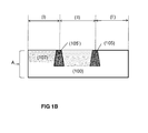
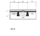
Figure 1 (D - F) illustrates schematically a method for manufacturing a hybrid MOSFET according to a first embodiment of the disclosure. -
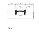
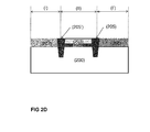
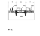
Figure 2 (A - E) illustrates schematically a method for manufacturing a hybrid MOSFET according to a second embodiment of the disclosure. -
Figure 3 (A - D) illustrates schematically a method for forming S/D contacts simultaneously on the first and the second MOSFET according to embodiments of the disclosure. - The present disclosure will be described with respect to particular embodiments and with reference to certain drawings but the disclosure is not limited thereto but only by the claims. The drawings described are only schematic and are non-limiting. In the drawings, the size of some of the elements may be exaggerated and not drawn on scale for illustrative purposes. The dimensions and the relative dimensions do not necessarily correspond to actual reductions to practice of the disclosure.
- Furthermore, the terms first, second, third and the like in the description and in the claims, are used for distinguishing between similar elements and not necessarily for describing a sequential or chronological order. The terms are interchangeable under appropriate circumstances and the embodiments of the disclosure can operate in other sequences than described or illustrated herein.
- Moreover, the terms top, bottom, over, under and the like in the description and the claims are used for descriptive purposes and not necessarily for describing relative positions. The terms so used are interchangeable under appropriate circumstances and the embodiments of the disclosure described herein can operate in other orientations than described or illustrated herein.
- Furthermore, the various embodiments, although referred to as "preferred" are to be construed as exemplary manners in which the disclosure may be implemented rather than as limiting the scope of the disclosure.
- The term "comprising", used in the claims, should not be interpreted as being restricted to the elements or steps listed thereafter; it does not exclude other elements or steps. It needs to be interpreted as specifying the presence of the stated features, integers, steps or components as referred to, but does not preclude the presence or addition of one or more other features, integers, steps or components, or groups thereof. Thus, the scope of the expression "a device comprising A and B" should not be limited to devices consisting only of components A and B, rather with respect to the present disclosure, the only enumerated components of the device are A and B, and further the claim should be interpreted as including equivalents of those components.
- Below, preferred embodiments according to this disclosure are presented for manufacturing a hybrid MOSFET device comprising a first MOSFET having a first channel comprising a group IV semiconductor material and a second MOSFET having a second channel comprising a III-V compound material. The device may further comprise a third MOSFET having a third channel comprising a group IV semiconductor material.
- Preferred embodiments provide a hybrid integration scheme for CMOS processing technology, whereby nMOS high mobility devices having a channel comprising a III-V compound material are fabricated on the same substrate and at the same time with pMOS high mobility devices and/or CMOS periphery devices. The nMOS high mobility devices are fabricated on regions with buried Insulator (III-V on insulator) while the other devices, i.e. pMOS high mobility devices and/or CMOS periphery devices are fabricated directly on bulk Si. Preferably, the pMOS high mobility devices have a germanium-comprising channel. Preferably, the CMOS periphery devices have a silicon-comprising channel.
- With reference to
Figs.1A-F a method for manufacturing a hybrid MOSFET is disclosed comprising the following steps. -
Fig. 1A shows that a III-V-on-insulator stack (C) is manufactured on a separate substrate according to a method which is known in the art and therefore needs no further description here. This separate substrate, herein called the second substrate or handle wafer, comprises a stack of a substrate layer (100'), a graded buffer layer (102), a III-V compound layer (103) which forms the III-V compound active layer, and an insulator layer (104). The substrate layer (100') can be a Si substrate (wafer) whereupon the buffer layer (102) and the III-V compound layer (103) are grown epitaxially. - Further, the graded buffer layer (102) can comprise one or more sub-layers, each sub-layer comprising a binary or a tertiary III-V compound. In preferred embodiments a sub-layer of the graded buffer layer (102) functions as etch stop layer, i.e is removable with a different chemistry than the substrate layer (100') and the layers of the graded buffer layer in between the substrate (100') and the etch stop layer.
- Further, the III-V layer (103) can comprise one or more sub-layers, each sub-layer comprising a binary or tertiary III-V compound. In specific examples the III-V layer (103) comprises InGaAs or InAs.
- The insulator layer (104) is preferably an oxide suitable to function as dielectric bonding layer. In specific embodiments the insulator layer (104) comprises silicon oxide or aluminum oxide.
-
Fig. 1B shows that a first substrate is provided, i.e. a device wafer, which is preferably a bulk semiconductor substrate (100). A first region (I, I') and a second region (II) are created by defining a shallow trench isolation pattern (105, 105') in the semiconductor substrate (100). In specific embodiments the group IV semiconductor material (107, 108) comprises silicon and/or germanium. Further in specific embodiments the group IV semiconductor material (107, 108) is germanium. -
Fig. 1C shows the direct substrate bonding of the first substrate (A) with the second substrate (B), such that a III-V-on-insulator stack (C) is provided on the first substrate (A), the III-V-on-insulator stack (C) comprising the insulating layer (104) overlying and in contact with the first substrate (A) over the first region (I, I') and a second region (II) and the III-V layer (103) overlying and in contact with the insulator layer (104) over the first region (I, I') and the second region (II). -
Fig. 1D shows the removal, preferably by etching, of the semiconductor substrate (100') and the graded buffer layer (102) after the direct substrate bonding, to expose the III-V layer. -
Fig. 1E shows the step of removing the III-V layer (103) and the insulator layer (104) selectively in the first region (I, I'), thereby exposing the semiconductor layer (107, 108) in the first region (I,I'). -
Fig. 1F shows the steps of forming a first and third gate stacks (109, 109') of first and third MOSFETs on the exposed semiconductor material in the first region (I, I') and forming a second gate stack (109") of the second MOSFET on the Ill-V layer in the second region (II). These steps are preferably, but not essentially, performed simultaneously. - In the sequence of
Fig. 1A-F , the shallow trench isolation pattern (105, 105') is defined in the semiconductor substrate (100) before (prior to the formation of) the III-V-on-insulator stack (C) on the substrate (100). Alternatively, as shown inFigs. 2A-B , the shallow trench isolation pattern (205, 205') may also be defined after the III-V-on-insulator stack (C, 203-204)) is bonded to the substrate (200). - In the sequence of
Fig. 1A-F , the first and third gate stacks (109, 109') are formed directly on top of the semiconductor material of the substrate (100), exposed by the removal of the III-V-on insulator stack in the second region (II). Alternatively, as shown inFigs. 2C-E , after removing the III-V-on-insulator stack (C) in the first region (I, I'), a second group IV semiconductor material (207, 208) is subsequently grown on the semiconductor substrate on the first region (I, I'), wherein the second group IV semiconductor material is suitable to function as the first channel material. In specific embodiments, the second group IV semiconductor material (207, 208) comprises silicon and/or germanium. In the embodiment ofFigs. 2A-E , the structure is further planarized prior to the formation of the gate stacks (209, 209', 209"). - In various embodiments of this disclosure the first MOSFET is a p-MOSFET and the second MOSFET is an n-MOSFET.
- In various embodiments of the disclosure the hybrid MOSFET device can comprise a third MOSFET on a third region (I'). In these embodiments the first and the second MOSFET are formed on, respectively, the first (I) and the second region (II) as described above and form together a high performance CMOS (core) device. The third MOSFET (e.g. a CMOS periphery) can be formed directly on the Si bulk substrate (100, 200, 300). The gate patterning and the further process integration of the three MOSFETs can be performed at the same time.
- An additional integration challenge is the formation of good contacts regions with an integration scheme which should be preferably compatible with the other devices like Si- or SiGe-based devices which are typically using silicide contacting schemes, such as e.g. NiSi.
- The method of the disclosure address this challenge by the sequence of
Figs. 3A-D with the following steps:Fig. 3C further removing the III-V-on-insulator stack (C) and creating a recess in the semiconductor substrate (300) in the areas corresponding to a source (S) and a drain (D) of the second MOSFET (II); followed by selective epitaxial re-growth of a doped group IV semiconductor material in each of the source (301) and the drain (301') recesses of the second MOSFET, thereafter forming source and drain contacts simultaneously on the first and the second MOSFET. - These additional process steps enable to use the same contacting scheme for both the high mobility devices and the Si CMOS periphery devices, e.g. Ni-silicide. The process conditions for the epitaxial re-growth of the S/D regions can be adapted such that the growth temperature is compatible with the III-V channel material.
- In different embodiments of the disclosure the III-V-on-insulator stack (C) can have a total thickness lower than 15 nm, preferably lower than 10nm. In other words, the sum of the thickness of the insulator layer (104) and the III-V layer (103) can be lower than 15 nm, preferably lower than 10 nm. A total thickness of the III-V-on-insulator stack (C) lower than 15nm makes possible that the patterning of the gate stacks of the first and second MOSFET can be performed at the same time, simplifying significantly the integration scheme.
Claims (16)
- A method for manufacturing a hybrid MOSFET device comprising a first MOSFET having a first channel material and a second MOSFET having a second channel material, comprising the following steps:providing a first substrate (A) comprising in at least a first region (I, I') a semiconductor layer (107, 108, 207, 208) of a group IV semiconductor material suitable to function as the first channel material;providing a second substrate (B) comprising a III-V layer (103) covered by and in contact with an exposed insulator layer (104), wherein the III-V layer comprises a III-V compound suitable to function as the second channel material;direct substrate bonding of the first substrate (A) with the second substrate (B), such that a III-V-on-insulator stack (C) is provided on the first substrate (A), the III-V-on-insulator stack (C) comprising the insulating layer (104, 204, 304) overlying and in contact with the first substrate (A) over the first region (I, I') and a second region (II) and the III-V layer (103, 203, 303) overlying and in contact with the insulator layer (104, 204, 304) over the first region (I, I') and the second region (II);removing the III-V layer (103, 203, 303) and the insulator layer (104, 204, 304) selectively in the first region (I, I'), thereby exposing the semiconductor layer (107, 108, 207, 208) in the first region (I, I');forming a first gate stack (109, 109') of the first MOSFET on the exposed semiconductor layer in the first region (I, I');forming a second gate stack (109") of the second MOSFET on the III-V layer in the second region (II).
- The method of claim 1, wherein the first and second gate stacks are formed simultaneously.
- The method of claim 1 or 2, wherein the second substrate (B) initially comprises a semiconductor substrate (100'), a graded buffer layer (102) on top of the semiconductor substrate, the III-V layer (103, 203, 303) on top of the graded buffer layer and the insulator layer (104, 204, 304) on top of the III-V layer, and wherein the semiconductor substrate (100') and the graded buffer layer (102) are removed after said direct substrate bonding to expose the III-V layer.
- The method of any one of the previous claims, wherein a shallow trench isolation pattern (105, 105') is formed in the first substrate (100) before the III-V-on-insulator stack (C) is provided thereon, to insulate the first region (I, I') from the second region (II).
- The method of any one of the claims 1-3, wherein a shallow trench isolation pattern (205, 205', 305, 305') is formed in the first substrate (200, 300) after the III-V-on-insulator stack (C) is provided thereon, to insulate the first region (I, I') from the second region (II).
- The method of any one of the preceding claims, wherein the group IV semiconductor material (107, 108) comprises silicon and/or germanium.
- The method of any one of the preceding claims, wherein after removing the III-V-on-insulator stack (C) in the first region (I, I'), a second group IV semiconductor material (207, 208) is subsequently grown on the exposed semiconductor layer in the first region (I, I'), wherein the second group IV semiconductor material is suitable to function as the first channel material.
- The method of any one of the preceding claims, wherein the second group IV semiconductor material (207, 208) comprises silicon and/or germanium.
- The method of any one of the preceding claims, wherein the first MOSFET is a p-MOSFET and the second MOSFET is an n-MOSFET.
- The method of any one of the preceding claims, further comprising removing the III-V-on-insulator stack (C) and creating recesses in the first substrate (300) in areas corresponding to source and drain areas of the second MOSFET (II), followed by selective epitaxial re-growth of a doped group IV semiconductor material in each of the source (301) and the drain (301') areas of the second MOSFET, followed by forming source and drain contacts simultaneously on the first and the second MOSFET.
- The method of any one of the preceding claims, wherein a sub-layer of the graded buffer layer (102) functions as etch stop layer.
- The method of any one of the preceding claims, wherein the insulator layer (104) comprises an oxide suitable to function as dielectric bonding layer.
- The method of any one of the preceding claims, wherein the insulator layer (104) comprises silicon oxide or aluminum oxide.
- The method of any one of the preceding claims, wherein the III-V-on-insulator stack (C) has a thickness lower than 15 nm, preferably lower than 10 nm.
- Hybrid MOSFET device comprising a first MOSFET having a first channel material and a second MOSFET having a second channel material, comprising:a first substrate (A) comprising in at least a first region (I, I') an exposed semiconductor layer (107, 108, 207, 208) of a group IV semiconductor material suitable to function as the first channel material;a III-V-on-insulator stack (C) is bonded to the first substrate (A), the III-V-on-insulator stack (C) comprising an insulating layer (104, 204, 304) overlying and in contact with the first substrate (A) over a second region (II) and a III-V layer (103, 203, 303) overlying and in contact with the insulator layer (104, 204, 304) over the second region (II), wherein the III-V layer comprises a III-V compound suitable to function as the second channel material;a first gate stack (109, 109') of the first MOSFET formed on the exposed semiconductor layer in the first region (I, I');a second gate stack (109") of the second MOSFET formed on the III-V layer in the second region (II).
- Hybrid MOSFET device according to claim 15, wherein the III-V-on-insulator stack (C) has a thickness lower than 15 nm, preferably lower than 10 nm.
Applications Claiming Priority (1)
| Application Number | Priority Date | Filing Date | Title |
|---|---|---|---|
| US201161482129P | 2011-05-03 | 2011-05-03 |
Publications (3)
| Publication Number | Publication Date |
|---|---|
| EP2521168A1 true EP2521168A1 (en) | 2012-11-07 |
| EP2521168B1 EP2521168B1 (en) | 2017-11-29 |
| EP2521168B8 EP2521168B8 (en) | 2018-01-10 |
Family
ID=46087497
Family Applications (1)
| Application Number | Title | Priority Date | Filing Date |
|---|---|---|---|
| EP12166646.5A Active EP2521168B8 (en) | 2011-05-03 | 2012-05-03 | Method for manufacturing a hybrid MOSFET device |
Country Status (3)
| Country | Link |
|---|---|
| US (1) | US8912055B2 (en) |
| EP (1) | EP2521168B8 (en) |
| JP (1) | JP6031253B2 (en) |
Cited By (3)
| Publication number | Priority date | Publication date | Assignee | Title |
|---|---|---|---|---|
| EP2849219A1 (en) * | 2013-09-11 | 2015-03-18 | IMEC vzw | Method for manufacturing transistors and associated substrate |
| WO2015065582A1 (en) * | 2013-10-28 | 2015-05-07 | Qualcomm Incorporated | Heterogeneous channel material integration into wafer |
| EP3084806A4 (en) * | 2013-12-18 | 2017-07-26 | Intel Corporation | Planar heterogeneous device |
Families Citing this family (1)
| Publication number | Priority date | Publication date | Assignee | Title |
|---|---|---|---|---|
| US9396948B2 (en) * | 2013-05-03 | 2016-07-19 | Texas Instruments Incorporated | Layer transfer of silicon onto III-nitride material for heterogenous integration |
Citations (5)
| Publication number | Priority date | Publication date | Assignee | Title |
|---|---|---|---|---|
| US5064781A (en) * | 1990-08-31 | 1991-11-12 | Motorola, Inc. | Method of fabricating integrated silicon and non-silicon semiconductor devices |
| US20040256700A1 (en) * | 2003-06-17 | 2004-12-23 | International Business Machines Corporation | High-performance CMOS devices on hybrid crystal oriented substrates |
| US20060172505A1 (en) * | 2005-01-31 | 2006-08-03 | Koester Steven J | Structure and method of integrating compound and elemental semiconductors for high-performace CMOS |
| US20070181977A1 (en) * | 2005-07-26 | 2007-08-09 | Amberwave Systems Corporation | Solutions for integrated circuit integration of alternative active area materials |
| US20080283958A1 (en) * | 2007-05-17 | 2008-11-20 | Semiconductor Energy Laboratory Co., Ltd. | Semiconductor device and method for manufacturing the same |
Family Cites Families (14)
| Publication number | Priority date | Publication date | Assignee | Title |
|---|---|---|---|---|
| JPH0824162B2 (en) * | 1989-07-10 | 1996-03-06 | 日本電装株式会社 | Semiconductor device and manufacturing method thereof |
| JP2605597B2 (en) * | 1993-09-09 | 1997-04-30 | 日本電気株式会社 | Method for manufacturing semiconductor device |
| US5894152A (en) | 1997-06-18 | 1999-04-13 | International Business Machines Corporation | SOI/bulk hybrid substrate and method of forming the same |
| US6563143B2 (en) | 1999-07-29 | 2003-05-13 | Stmicroelectronics, Inc. | CMOS circuit of GaAs/Ge on Si substrate |
| US7034362B2 (en) * | 2003-10-17 | 2006-04-25 | International Business Machines Corporation | Double silicon-on-insulator (SOI) metal oxide semiconductor field effect transistor (MOSFET) structures |
| US7208815B2 (en) | 2004-05-28 | 2007-04-24 | Taiwan Semiconductor Manufacturing Company, Ltd. | CMOS logic gate fabricated on hybrid crystal orientations and method of forming thereof |
| US20050275018A1 (en) * | 2004-06-10 | 2005-12-15 | Suresh Venkatesan | Semiconductor device with multiple semiconductor layers |
| US7560322B2 (en) * | 2004-10-27 | 2009-07-14 | Northrop Grumman Systems Corporation | Method of making a semiconductor structure for high power semiconductor devices |
| US7385257B2 (en) | 2006-04-26 | 2008-06-10 | International Business Machines Corporation | Hybrid orientation SOI substrates, and method for forming the same |
| US7749829B2 (en) * | 2007-05-01 | 2010-07-06 | Freescale Semiconductor, Inc. | Step height reduction between SOI and EPI for DSO and BOS integration |
| US7790528B2 (en) | 2007-05-01 | 2010-09-07 | Freescale Semiconductor, Inc. | Dual substrate orientation or bulk on SOI integrations using oxidation for silicon epitaxy spacer formation |
| FR2917235B1 (en) | 2007-06-06 | 2010-09-03 | Soitec Silicon On Insulator | METHOD FOR PRODUCING HYBRID COMPONENTS |
| JP2009212413A (en) * | 2008-03-06 | 2009-09-17 | Renesas Technology Corp | Semiconductor device and method of manufacturing semiconductor device |
| EP2254148B1 (en) * | 2009-05-18 | 2011-11-30 | S.O.I.Tec Silicon on Insulator Technologies | Fabrication process of a hybrid semiconductor substrate |
-
2012
- 2012-05-02 US US13/462,694 patent/US8912055B2/en active Active
- 2012-05-03 EP EP12166646.5A patent/EP2521168B8/en active Active
- 2012-05-07 JP JP2012105801A patent/JP6031253B2/en active Active
Patent Citations (5)
| Publication number | Priority date | Publication date | Assignee | Title |
|---|---|---|---|---|
| US5064781A (en) * | 1990-08-31 | 1991-11-12 | Motorola, Inc. | Method of fabricating integrated silicon and non-silicon semiconductor devices |
| US20040256700A1 (en) * | 2003-06-17 | 2004-12-23 | International Business Machines Corporation | High-performance CMOS devices on hybrid crystal oriented substrates |
| US20060172505A1 (en) * | 2005-01-31 | 2006-08-03 | Koester Steven J | Structure and method of integrating compound and elemental semiconductors for high-performace CMOS |
| US20070181977A1 (en) * | 2005-07-26 | 2007-08-09 | Amberwave Systems Corporation | Solutions for integrated circuit integration of alternative active area materials |
| US20080283958A1 (en) * | 2007-05-17 | 2008-11-20 | Semiconductor Energy Laboratory Co., Ltd. | Semiconductor device and method for manufacturing the same |
Cited By (5)
| Publication number | Priority date | Publication date | Assignee | Title |
|---|---|---|---|---|
| EP2849219A1 (en) * | 2013-09-11 | 2015-03-18 | IMEC vzw | Method for manufacturing transistors and associated substrate |
| WO2015065582A1 (en) * | 2013-10-28 | 2015-05-07 | Qualcomm Incorporated | Heterogeneous channel material integration into wafer |
| US9257407B2 (en) | 2013-10-28 | 2016-02-09 | Qualcomm Incorporated | Heterogeneous channel material integration into wafer |
| EP3084806A4 (en) * | 2013-12-18 | 2017-07-26 | Intel Corporation | Planar heterogeneous device |
| US10014374B2 (en) | 2013-12-18 | 2018-07-03 | Intel Corporation | Planar heterogeneous device |
Also Published As
| Publication number | Publication date |
|---|---|
| US8912055B2 (en) | 2014-12-16 |
| JP2012248830A (en) | 2012-12-13 |
| EP2521168B8 (en) | 2018-01-10 |
| JP6031253B2 (en) | 2016-11-24 |
| US20120280326A1 (en) | 2012-11-08 |
| EP2521168B1 (en) | 2017-11-29 |
Similar Documents
| Publication | Publication Date | Title |
|---|---|---|
| US12027607B2 (en) | Methods for GAA I/O formation by selective epi regrowth | |
| JP5464850B2 (en) | Method for manufacturing a multi-gate semiconductor device having improved carrier mobility | |
| EP2682983B1 (en) | CMOS device comprising silicon and germanium and method for manufacturing thereof | |
| US7034362B2 (en) | Double silicon-on-insulator (SOI) metal oxide semiconductor field effect transistor (MOSFET) structures | |
| US8697523B2 (en) | Integration of SMT in replacement gate FINFET process flow | |
| US7790528B2 (en) | Dual substrate orientation or bulk on SOI integrations using oxidation for silicon epitaxy spacer formation | |
| JP5203352B2 (en) | Method of manufacturing a semiconductor using an etching stop layer to optimize the formation of a source / drain stressor | |
| US7435639B2 (en) | Dual surface SOI by lateral epitaxial overgrowth | |
| CN104350597B (en) | Field Effect Transistors with Mixed Channel Materials | |
| US7803670B2 (en) | Twisted dual-substrate orientation (DSO) substrates | |
| US7439542B2 (en) | Hybrid orientation CMOS with partial insulation process | |
| JP2009200471A5 (en) | ||
| CN100411180C (en) | Semiconductor structure and method of manufacturing semiconductor structure | |
| US20060172505A1 (en) | Structure and method of integrating compound and elemental semiconductors for high-performace CMOS | |
| KR20150044412A (en) | Finfet with buried insulator layer and method for forming | |
| KR20140143869A (en) | Semiconductor device having strained channel layer and method of manufacturing the same | |
| US7544548B2 (en) | Trench liner for DSO integration | |
| EP2521168B1 (en) | Method for manufacturing a hybrid MOSFET device | |
| US10615178B2 (en) | Dual-material mandrel for epitaxial crystal growth on silicon | |
| CN102315126A (en) | Semiconductor device and manufacturing method thereof |
Legal Events
| Date | Code | Title | Description |
|---|---|---|---|
| PUAI | Public reference made under article 153(3) epc to a published international application that has entered the european phase |
Free format text: ORIGINAL CODE: 0009012 |
|
| AK | Designated contracting states |
Kind code of ref document: A1 Designated state(s): AL AT BE BG CH CY CZ DE DK EE ES FI FR GB GR HR HU IE IS IT LI LT LU LV MC MK MT NL NO PL PT RO RS SE SI SK SM TR |
|
| AX | Request for extension of the european patent |
Extension state: BA ME |
|
| 17P | Request for examination filed |
Effective date: 20130507 |
|
| 17Q | First examination report despatched |
Effective date: 20140108 |
|
| GRAP | Despatch of communication of intention to grant a patent |
Free format text: ORIGINAL CODE: EPIDOSNIGR1 |
|
| STAA | Information on the status of an ep patent application or granted ep patent |
Free format text: STATUS: GRANT OF PATENT IS INTENDED |
|
| RIC1 | Information provided on ipc code assigned before grant |
Ipc: H01L 21/28 20060101ALI20170524BHEP Ipc: H01L 29/66 20060101ALI20170524BHEP Ipc: H01L 21/8258 20060101AFI20170524BHEP Ipc: H01L 29/78 20060101ALI20170524BHEP Ipc: H01L 29/10 20060101ALI20170524BHEP |
|
| INTG | Intention to grant announced |
Effective date: 20170620 |
|
| GRAS | Grant fee paid |
Free format text: ORIGINAL CODE: EPIDOSNIGR3 |
|
| GRAA | (expected) grant |
Free format text: ORIGINAL CODE: 0009210 |
|
| STAA | Information on the status of an ep patent application or granted ep patent |
Free format text: STATUS: THE PATENT HAS BEEN GRANTED |
|
| AK | Designated contracting states |
Kind code of ref document: B1 Designated state(s): AL AT BE BG CH CY CZ DE DK EE ES FI FR GB GR HR HU IE IS IT LI LT LU LV MC MK MT NL NO PL PT RO RS SE SI SK SM TR |
|
| REG | Reference to a national code |
Ref country code: CH Ref legal event code: EP |
|
| REG | Reference to a national code |
Ref country code: AT Ref legal event code: REF Ref document number: 951112 Country of ref document: AT Kind code of ref document: T Effective date: 20171215 |
|
| RAP2 | Party data changed (patent owner data changed or rights of a patent transferred) |
Owner name: IMEC VZW |
|
| REG | Reference to a national code |
Ref country code: IE Ref legal event code: FG4D |
|
| REG | Reference to a national code |
Ref country code: DE Ref legal event code: R096 Ref document number: 602012040257 Country of ref document: DE |
|
| REG | Reference to a national code |
Ref country code: NL Ref legal event code: MP Effective date: 20171129 |
|
| REG | Reference to a national code |
Ref country code: LT Ref legal event code: MG4D |
|
| REG | Reference to a national code |
Ref country code: AT Ref legal event code: MK05 Ref document number: 951112 Country of ref document: AT Kind code of ref document: T Effective date: 20171129 |
|
| REG | Reference to a national code |
Ref country code: FR Ref legal event code: PLFP Year of fee payment: 7 |
|
| PG25 | Lapsed in a contracting state [announced via postgrant information from national office to epo] |
Ref country code: ES Free format text: LAPSE BECAUSE OF FAILURE TO SUBMIT A TRANSLATION OF THE DESCRIPTION OR TO PAY THE FEE WITHIN THE PRESCRIBED TIME-LIMIT Effective date: 20171129 Ref country code: LT Free format text: LAPSE BECAUSE OF FAILURE TO SUBMIT A TRANSLATION OF THE DESCRIPTION OR TO PAY THE FEE WITHIN THE PRESCRIBED TIME-LIMIT Effective date: 20171129 Ref country code: FI Free format text: LAPSE BECAUSE OF FAILURE TO SUBMIT A TRANSLATION OF THE DESCRIPTION OR TO PAY THE FEE WITHIN THE PRESCRIBED TIME-LIMIT Effective date: 20171129 Ref country code: NO Free format text: LAPSE BECAUSE OF FAILURE TO SUBMIT A TRANSLATION OF THE DESCRIPTION OR TO PAY THE FEE WITHIN THE PRESCRIBED TIME-LIMIT Effective date: 20180228 Ref country code: SE Free format text: LAPSE BECAUSE OF FAILURE TO SUBMIT A TRANSLATION OF THE DESCRIPTION OR TO PAY THE FEE WITHIN THE PRESCRIBED TIME-LIMIT Effective date: 20171129 |
|
| PG25 | Lapsed in a contracting state [announced via postgrant information from national office to epo] |
Ref country code: AT Free format text: LAPSE BECAUSE OF FAILURE TO SUBMIT A TRANSLATION OF THE DESCRIPTION OR TO PAY THE FEE WITHIN THE PRESCRIBED TIME-LIMIT Effective date: 20171129 Ref country code: BG Free format text: LAPSE BECAUSE OF FAILURE TO SUBMIT A TRANSLATION OF THE DESCRIPTION OR TO PAY THE FEE WITHIN THE PRESCRIBED TIME-LIMIT Effective date: 20180228 Ref country code: GR Free format text: LAPSE BECAUSE OF FAILURE TO SUBMIT A TRANSLATION OF THE DESCRIPTION OR TO PAY THE FEE WITHIN THE PRESCRIBED TIME-LIMIT Effective date: 20180301 Ref country code: LV Free format text: LAPSE BECAUSE OF FAILURE TO SUBMIT A TRANSLATION OF THE DESCRIPTION OR TO PAY THE FEE WITHIN THE PRESCRIBED TIME-LIMIT Effective date: 20171129 Ref country code: RS Free format text: LAPSE BECAUSE OF FAILURE TO SUBMIT A TRANSLATION OF THE DESCRIPTION OR TO PAY THE FEE WITHIN THE PRESCRIBED TIME-LIMIT Effective date: 20171129 Ref country code: HR Free format text: LAPSE BECAUSE OF FAILURE TO SUBMIT A TRANSLATION OF THE DESCRIPTION OR TO PAY THE FEE WITHIN THE PRESCRIBED TIME-LIMIT Effective date: 20171129 |
|
| PG25 | Lapsed in a contracting state [announced via postgrant information from national office to epo] |
Ref country code: NL Free format text: LAPSE BECAUSE OF FAILURE TO SUBMIT A TRANSLATION OF THE DESCRIPTION OR TO PAY THE FEE WITHIN THE PRESCRIBED TIME-LIMIT Effective date: 20171129 |
|
| PG25 | Lapsed in a contracting state [announced via postgrant information from national office to epo] |
Ref country code: SK Free format text: LAPSE BECAUSE OF FAILURE TO SUBMIT A TRANSLATION OF THE DESCRIPTION OR TO PAY THE FEE WITHIN THE PRESCRIBED TIME-LIMIT Effective date: 20171129 Ref country code: CZ Free format text: LAPSE BECAUSE OF FAILURE TO SUBMIT A TRANSLATION OF THE DESCRIPTION OR TO PAY THE FEE WITHIN THE PRESCRIBED TIME-LIMIT Effective date: 20171129 Ref country code: CY Free format text: LAPSE BECAUSE OF FAILURE TO SUBMIT A TRANSLATION OF THE DESCRIPTION OR TO PAY THE FEE WITHIN THE PRESCRIBED TIME-LIMIT Effective date: 20171129 Ref country code: DK Free format text: LAPSE BECAUSE OF FAILURE TO SUBMIT A TRANSLATION OF THE DESCRIPTION OR TO PAY THE FEE WITHIN THE PRESCRIBED TIME-LIMIT Effective date: 20171129 Ref country code: EE Free format text: LAPSE BECAUSE OF FAILURE TO SUBMIT A TRANSLATION OF THE DESCRIPTION OR TO PAY THE FEE WITHIN THE PRESCRIBED TIME-LIMIT Effective date: 20171129 |
|
| REG | Reference to a national code |
Ref country code: DE Ref legal event code: R097 Ref document number: 602012040257 Country of ref document: DE |
|
| PG25 | Lapsed in a contracting state [announced via postgrant information from national office to epo] |
Ref country code: PL Free format text: LAPSE BECAUSE OF FAILURE TO SUBMIT A TRANSLATION OF THE DESCRIPTION OR TO PAY THE FEE WITHIN THE PRESCRIBED TIME-LIMIT Effective date: 20171129 Ref country code: RO Free format text: LAPSE BECAUSE OF FAILURE TO SUBMIT A TRANSLATION OF THE DESCRIPTION OR TO PAY THE FEE WITHIN THE PRESCRIBED TIME-LIMIT Effective date: 20171129 Ref country code: IT Free format text: LAPSE BECAUSE OF FAILURE TO SUBMIT A TRANSLATION OF THE DESCRIPTION OR TO PAY THE FEE WITHIN THE PRESCRIBED TIME-LIMIT Effective date: 20171129 Ref country code: SM Free format text: LAPSE BECAUSE OF FAILURE TO SUBMIT A TRANSLATION OF THE DESCRIPTION OR TO PAY THE FEE WITHIN THE PRESCRIBED TIME-LIMIT Effective date: 20171129 |
|
| PLBE | No opposition filed within time limit |
Free format text: ORIGINAL CODE: 0009261 |
|
| STAA | Information on the status of an ep patent application or granted ep patent |
Free format text: STATUS: NO OPPOSITION FILED WITHIN TIME LIMIT |
|
| 26N | No opposition filed |
Effective date: 20180830 |
|
| PG25 | Lapsed in a contracting state [announced via postgrant information from national office to epo] |
Ref country code: SI Free format text: LAPSE BECAUSE OF FAILURE TO SUBMIT A TRANSLATION OF THE DESCRIPTION OR TO PAY THE FEE WITHIN THE PRESCRIBED TIME-LIMIT Effective date: 20171129 |
|
| REG | Reference to a national code |
Ref country code: CH Ref legal event code: PL |
|
| GBPC | Gb: european patent ceased through non-payment of renewal fee |
Effective date: 20180503 |
|
| REG | Reference to a national code |
Ref country code: BE Ref legal event code: MM Effective date: 20180531 |
|
| PG25 | Lapsed in a contracting state [announced via postgrant information from national office to epo] |
Ref country code: MC Free format text: LAPSE BECAUSE OF FAILURE TO SUBMIT A TRANSLATION OF THE DESCRIPTION OR TO PAY THE FEE WITHIN THE PRESCRIBED TIME-LIMIT Effective date: 20171129 |
|
| REG | Reference to a national code |
Ref country code: IE Ref legal event code: MM4A |
|
| PG25 | Lapsed in a contracting state [announced via postgrant information from national office to epo] |
Ref country code: CH Free format text: LAPSE BECAUSE OF NON-PAYMENT OF DUE FEES Effective date: 20180531 Ref country code: LI Free format text: LAPSE BECAUSE OF NON-PAYMENT OF DUE FEES Effective date: 20180531 |
|
| PG25 | Lapsed in a contracting state [announced via postgrant information from national office to epo] |
Ref country code: LU Free format text: LAPSE BECAUSE OF NON-PAYMENT OF DUE FEES Effective date: 20180503 |
|
| PG25 | Lapsed in a contracting state [announced via postgrant information from national office to epo] |
Ref country code: GB Free format text: LAPSE BECAUSE OF NON-PAYMENT OF DUE FEES Effective date: 20180503 Ref country code: IE Free format text: LAPSE BECAUSE OF NON-PAYMENT OF DUE FEES Effective date: 20180503 |
|
| PG25 | Lapsed in a contracting state [announced via postgrant information from national office to epo] |
Ref country code: BE Free format text: LAPSE BECAUSE OF NON-PAYMENT OF DUE FEES Effective date: 20180531 |
|
| PG25 | Lapsed in a contracting state [announced via postgrant information from national office to epo] |
Ref country code: MT Free format text: LAPSE BECAUSE OF NON-PAYMENT OF DUE FEES Effective date: 20180503 |
|
| PG25 | Lapsed in a contracting state [announced via postgrant information from national office to epo] |
Ref country code: TR Free format text: LAPSE BECAUSE OF FAILURE TO SUBMIT A TRANSLATION OF THE DESCRIPTION OR TO PAY THE FEE WITHIN THE PRESCRIBED TIME-LIMIT Effective date: 20171129 |
|
| PG25 | Lapsed in a contracting state [announced via postgrant information from national office to epo] |
Ref country code: PT Free format text: LAPSE BECAUSE OF FAILURE TO SUBMIT A TRANSLATION OF THE DESCRIPTION OR TO PAY THE FEE WITHIN THE PRESCRIBED TIME-LIMIT Effective date: 20171129 Ref country code: HU Free format text: LAPSE BECAUSE OF FAILURE TO SUBMIT A TRANSLATION OF THE DESCRIPTION OR TO PAY THE FEE WITHIN THE PRESCRIBED TIME-LIMIT; INVALID AB INITIO Effective date: 20120503 |
|
| PG25 | Lapsed in a contracting state [announced via postgrant information from national office to epo] |
Ref country code: MK Free format text: LAPSE BECAUSE OF NON-PAYMENT OF DUE FEES Effective date: 20171129 |
|
| PG25 | Lapsed in a contracting state [announced via postgrant information from national office to epo] |
Ref country code: AL Free format text: LAPSE BECAUSE OF FAILURE TO SUBMIT A TRANSLATION OF THE DESCRIPTION OR TO PAY THE FEE WITHIN THE PRESCRIBED TIME-LIMIT Effective date: 20171129 Ref country code: IS Free format text: LAPSE BECAUSE OF FAILURE TO SUBMIT A TRANSLATION OF THE DESCRIPTION OR TO PAY THE FEE WITHIN THE PRESCRIBED TIME-LIMIT Effective date: 20180329 |
|
| P01 | Opt-out of the competence of the unified patent court (upc) registered |
Effective date: 20230513 |
|
| REG | Reference to a national code |
Ref country code: DE Ref legal event code: R079 Ref document number: 602012040257 Country of ref document: DE Free format text: PREVIOUS MAIN CLASS: H01L0021825800 Ipc: H10D0084080000 |
|
| PGFP | Annual fee paid to national office [announced via postgrant information from national office to epo] |
Ref country code: DE Payment date: 20250423 Year of fee payment: 14 |
|
| PGFP | Annual fee paid to national office [announced via postgrant information from national office to epo] |
Ref country code: FR Payment date: 20250423 Year of fee payment: 14 |