EP2520943A2 - Apparatus for detecting partial discharge for electric power devices - Google Patents
Apparatus for detecting partial discharge for electric power devices Download PDFInfo
- Publication number
- EP2520943A2 EP2520943A2 EP10841202A EP10841202A EP2520943A2 EP 2520943 A2 EP2520943 A2 EP 2520943A2 EP 10841202 A EP10841202 A EP 10841202A EP 10841202 A EP10841202 A EP 10841202A EP 2520943 A2 EP2520943 A2 EP 2520943A2
- Authority
- EP
- European Patent Office
- Prior art keywords
- partial discharge
- signal
- receiving
- band
- detecting apparatus
- Prior art date
- Legal status (The legal status is an assumption and is not a legal conclusion. Google has not performed a legal analysis and makes no representation as to the accuracy of the status listed.)
- Granted
Links
Images



Classifications
-
- G—PHYSICS
- G01—MEASURING; TESTING
- G01R—MEASURING ELECTRIC VARIABLES; MEASURING MAGNETIC VARIABLES
- G01R31/00—Arrangements for testing electric properties; Arrangements for locating electric faults; Arrangements for electrical testing characterised by what is being tested not provided for elsewhere
- G01R31/12—Testing dielectric strength or breakdown voltage ; Testing or monitoring effectiveness or level of insulation, e.g. of a cable or of an apparatus, for example using partial discharge measurements; Electrostatic testing
-
- G—PHYSICS
- G01—MEASURING; TESTING
- G01R—MEASURING ELECTRIC VARIABLES; MEASURING MAGNETIC VARIABLES
- G01R31/00—Arrangements for testing electric properties; Arrangements for locating electric faults; Arrangements for electrical testing characterised by what is being tested not provided for elsewhere
- G01R31/12—Testing dielectric strength or breakdown voltage ; Testing or monitoring effectiveness or level of insulation, e.g. of a cable or of an apparatus, for example using partial discharge measurements; Electrostatic testing
- G01R31/1227—Testing dielectric strength or breakdown voltage ; Testing or monitoring effectiveness or level of insulation, e.g. of a cable or of an apparatus, for example using partial discharge measurements; Electrostatic testing of components, parts or materials
-
- G—PHYSICS
- G01—MEASURING; TESTING
- G01R—MEASURING ELECTRIC VARIABLES; MEASURING MAGNETIC VARIABLES
- G01R29/00—Arrangements for measuring or indicating electric quantities not covered by groups G01R19/00 - G01R27/00
- G01R29/08—Measuring electromagnetic field characteristics
- G01R29/0864—Measuring electromagnetic field characteristics characterised by constructional or functional features
- G01R29/0878—Sensors; antennas; probes; detectors
-
- G—PHYSICS
- G01—MEASURING; TESTING
- G01R—MEASURING ELECTRIC VARIABLES; MEASURING MAGNETIC VARIABLES
- G01R31/00—Arrangements for testing electric properties; Arrangements for locating electric faults; Arrangements for electrical testing characterised by what is being tested not provided for elsewhere
- G01R31/12—Testing dielectric strength or breakdown voltage ; Testing or monitoring effectiveness or level of insulation, e.g. of a cable or of an apparatus, for example using partial discharge measurements; Electrostatic testing
- G01R31/14—Circuits therefor, e.g. for generating test voltages, sensing circuits
-
- G—PHYSICS
- G01—MEASURING; TESTING
- G01R—MEASURING ELECTRIC VARIABLES; MEASURING MAGNETIC VARIABLES
- G01R31/00—Arrangements for testing electric properties; Arrangements for locating electric faults; Arrangements for electrical testing characterised by what is being tested not provided for elsewhere
- G01R31/50—Testing of electric apparatus, lines, cables or components for short-circuits, continuity, leakage current or incorrect line connections
- G01R31/62—Testing of transformers
Definitions
- the present invention relates to an apparatus for detecting partial discharge for an electric power device, and more particularly, to a partial discharge detecting apparatus for an electric power device that may measure signals of multiple frequency bands in which the electric power device may correspond to a power transformer and the electric power device may include a rotary device, a motor, a generator, and the like.
- a general partial discharge detecting apparatus for a power transformer may be installed inside an electric power device while maintaining a predetermined insulating distance and thereby detect a partial discharge signal.
- An installation type of the detecting apparatus may be classified into two types based on an installation location.
- the conventional partial discharge detecting apparatus may prevent leakage of insulating oil and may stably detect a partial discharge signal in a state where the insulating oil is filled. Also, the conventional partial discharge detecting apparatus may detect a partial discharge signal using a receiving unit having a wide width, such as a sensor applied to a gas insulating device. In addition, when an inspection window provided to the conventional partial discharge detecting apparatus is the same as the gas insulating device, the inspection window may be used compatibly with a partial discharge detecting apparatus of the gas insulating device.
- the conventional partial discharge detecting apparatus may not additionally include a separate inspection window and a sensor may be installed at various locations, for example, an upper portion, a lower portion, a side, and the like.
- the conventional partial discharge detecting apparatus is installed in a state where leakage of insulating oil is prevented using a valve and thus, may be stably mounted.
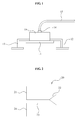
- FIGS. 1 and 2 are views illustrating the conventional partial discharge detecting apparatus.
- a conventional partial discharge detecting apparatus 10 is installed in an upper portion of a power transformer.
- the partial discharge detecting apparatus 10 may include a receiving unit 11 and inspection windows 12 and 13, and may transmit, via an N-type connector 14 and a coaxial cable 15, a signal that is detected from the power transformer.
- a conventional partial discharge detecting apparatus 20 is installed in a drain valve.
- the partial discharge detecting apparatus 20 may separately include a signal unit end 21 and a signal output end 22, and may include a receiving unit 23a connected to an input and a receiving unit 23b connected to an output in a parallel coupler form.
- a sensor when a partial discharge detecting apparatus is installed in an upper portion of a power transformer, a sensor may not be installed. Even though a sensor may be installable, the range of partial discharge signal detection may be restricted due to a limited installation location of the sensor. Also, a partial discharge signal occurring in a lower portion of the power transformer may be attenuated due to a distance and an internal constituent element, for example, due to the affect of insulating oil, winding, and the like. Accordingly, it may be difficult to detect a signal.
- the partial discharge detecting apparatus when the partial discharge detecting apparatus is installed in a drain valve, an input and an output may be separately provided and thus, the partial discharge detecting apparatus may have a coupler function in addition to an antenna function to thereby be capable of injecting a signal and obtaining an output signal.
- the partial discharge detecting apparatus is installed in a drain valve capable of preventing leakage of insulating oil to thereby have a structure in which installation and separation may be readily performed.
- the partial discharge detecting apparatus is generally configured in a form of a circle, two semicircles having the same shape, or a long monopole and thus, may have difficult in detecting a wideband signal.
- the partial discharge detecting apparatus is configured in a unit shape and the same shape to be capable of having the fixed wavelength.
- a size of a dipole antenna structure may be determined based on a length of a wavelength shown in FIG. 3 .
- the partial discharge detecting apparatus has a narrow bandwidth having a unit resonant frequency and thus, may have some constraints in detecting a partial discharge signal of a wide band in the case of detecting the partial discharge.
- a frequency band in which the partial discharge occurs is generally 0.5 GHz to 1.5 GHz and a wideband characteristic is required to receive a signal of a wide frequency band.
- the partial discharge detecting apparatus is configured in the unit shape and the same shape, the wavelength is physically constrained to have a wideband and thus, it may be difficult to configure the partial discharge detecting apparatus.
- Embodiments of the present invention provide an apparatus for detecting partial discharge that may detect a partial discharge signal of an electric power device, for example, a power transformer through a plurality of sub-bands.
- embodiments of the present invention provide an apparatus for detecting partial discharge for an electric power device that may selectively detect a partial discharge signal of a designated frequency band.
- an apparatus for detecting partial charge for an electric power device including: an insulator having a predetermined shape; a receiving unit including at least one receiving electrode that is installed inside or outside the insulator to receive a signal of each of at least one sub-band; and a connection electrode to transmit a signal of each of the at least one receiving electrode to a coaxial cable in conjunction with the connected coaxial cable.
- the at least one sub-band may correspond to a plurality of signal bands that is divided to detect a partial discharge signal of a power transformer in the entire frequency band.
- the receiving unit may be provided in a monopole structure.
- the receiving unit may include the at least one receiving electrode to receive a signal of each sub-band.
- each of the at least one receiving electrode may have a different wavelength to measure a signal of each sub-band.
- the at least one receiving electrode may be disposed to face each other based on the insulator.
- a partial discharge detecting apparatus may process a frequency signal of a wideband by receiving signals of a wide frequency band via a plurality of sub-bands.
- a partial discharge detecting apparatus may be configured to detect a signal of a desired band by selectively installing a receiving electrode having a different wavelength for each sub-band.
- a partial discharge detecting apparatus may be applicable to a power electric device.
- the power electric device may correspond to a power transformer.
- the power electric device may include a rotary device, a motor, a generator, and the like.
- a description will be made using the power transformer as the power electric device applied with the partial discharge detecting apparatus.
- FIG. 4 is a view illustrating a partial discharge detecting apparatus according to an embodiment of the present invention.
- the partial discharge detecting apparatus 100 may be installed in an upper portion of a power transformer 30 or a lower drain valve 40.
- the partial discharge detecting apparatus 100 may interact with a partial discharge signal processing apparatus 400 via an N-type connector 200 and a coaxial cable 300.
- the partial discharge detecting apparatus 100 may include a receiving unit to detect a signal of each of multiple sub-bands.
- a receiving unit to detect a signal of each of multiple sub-bands.
- the receiving unit of the partial discharge detecting apparatus 100 may be provided for each of the plurality of sub-bands of the partial discharge signal band, for example, four frequency bands including a first band of 0.5 GHz to 0.75 GHz, a second band of 0.75 GHz to 1.00 GHz, a third band of 1.00 GHz to 1.25 GHz, and a fourth band of 1.25 GHz to 1.5 GHz.
- a structure of the receiving unit may be configured as one of a meander-line structure, a rectangular spiral structure, and a symmetrical structure in which the same electrodes face each other. Due to characteristics, the structure of the receiving unit may have a wide wavelength with a narrow area.
- the receiving unit may be attached on an outside of an insulator of the partial discharge detecting apparatus 100 or may be inserted into the partial discharge detecting apparatus 100.
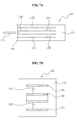
- FIGS. 5A and 5B show the partial discharge detecting apparatus 100 in a case where a receiving unit is installed outside an insulator.
- FIG. 5A shows a longitudinal-side view of the partial discharge detecting apparatus 100
- FIG. 5B shows a cross-sectional view of the partial discharge detecting apparatus 100.
- the partial discharge detecting apparatus 100 may include an insulator 120, a receiving unit (131 to 133), a lower electrode 140, and a connection electrode 110.
- the insulator 120 may be configured in a predetermined shape, for example, an equiangular shape such as a rectangular shape or a hexagonal shape, and may be formed using acryl or epoxy solid against heat.
- the receiving unit (131 to 134) may be provided inside or outside the insulator 120 to receive a signal of each of a plurality of sub-bands.
- the receiving unit (131 to 134) may include at least one receiving electrode, for example, receiving electrodes 131 to 134, to receive a signal of each sub-band.
- the sub-band may correspond to a plurality of signal bands for detecting a partial discharge signal of the power transformer in the entire frequency band.
- the receiving electrodes 131 to 134 may be provided for the respective sub-bands.
- Aluminum and stainless materials may be used as a material of the receiving electrodes 131 to 134 to minimize erosion occurring due to insulating oil.
- Each of the receiving electrodes 131 to 134 may be positioned to surround the insulator 120 and be connected to the lower electrode 140.
- the lower electrode 140 may be connected to the N-type connector 200 via the connection electrode 110.
- each of the receiving electrodes 131 to 134 may be configured to have a 1/4 wavelength of a different band. Accordingly, the partial discharge detecting apparatus may detect signals of multiple bands.
- the receiving electrodes 131 to 134 may be disposed to face each other based on the insulator 120. Accordingly, capacitance may be present between predetermined receiving electrodes, for example, between the receiving electrodes 131 and 133, and between the receiving electrodes 132 and 134.
- a predetermined parallel resonance circuit may be formed in the receiving electrodes 131 to 134 that function as a receiving unit of an antenna.
- the receiving electrodes 131 to 134 have the same clearance based on the insulator 120 and thus, the same capacitance may be present.
- the entire resonance circuit may have different resonant frequencies due to inductance that forms different wavelengths.
- inductance of the receiving electrode 131 may form different four resonant frequencies overall. Since a parallel resonance circuit corresponds to adjacent four parallel circuits, an additional band may be formed due to interaction between adjacent circuits.
- FIGS. 7A and 7B show a partial discharge detecting apparatus 101 in a case where a receiving unit (135 to 137) is provided inside an insulator 121.
- the partial discharge detecting apparatus 101 may include a lower electrode 141, and a connection electrode 111.
- FIG. 7A shows a longitudinal-side view of the partial discharge detecting apparatus 101
- FIG. 7B shows a cross-sectional view of the partial discharge detecting apparatus 101.
- the receiving unit (135 to 137, 151, and 152) of the partial discharge detecting apparatus 101 may be provided inside the insulator 121 and be fixed to be in parallel with each other.
- the receiving unit (135 to 137, 151, and 152) may include a plurality of receiving electrodes 135 to 137 and at least one parallel maintaining electrode, for example, parallel maintaining electrodes 151 and 152.
- the receiving electrodes 135 to 137 may be installed inside the insulator 121, and a plurality of electrode boards may be provided to be in parallel with each other in order to be capable of receiving a signal for each sub-band.
- the parallel maintaining electrodes 151 and 152 may be inserted to maintain a parallel relationship between the respective receiving electrodes 135 to 137, and may be formed using the same material as the receiving electrodes 135 to 137.
- the insulator 121 may be configured to mold the internally installed receiving unit (135 to 137, 151, and 152).
- the insulator 121 may be formed using a material having a high conductivity such as copper, aluminum, and stainless to prevent the molded receiving unit (135 to 137, 151, and 152) from being eroded due to insulating oil.
- the receiving electrodes 135 to 137 may be arranged inside the insulator 121 to be in parallel with each other at predetermined intervals, and may be connected to each other via the respective connection electrodes 151 and 152.
- the receiving electrodes 135 to 137 may maintain the capacitance between the respective receiving electrodes at predetermined intervals.
- a multi-resonance circuit may be present.
- a wideband detecting apparatus may be required and a multi-resonance scheme may be employed to configure the above purpose.
- FIG. 9 is a graph showing a return loss of a partial discharge detecting apparatus according to an embodiment of the present invention.
- the return loss graph shows a test result that is obtained by connecting the partial discharge detecting apparatus 100 or 101 to a chamber for simulation test of a power transformer, and shows signals that are measured using four sub-bands A to D.
- each of the sub-bands A to D may be designed to be suitable for a 1/4 wavelength of a resonant frequency for each band.
- four frequency bands may include a first band of 0.5 GHz to 0.75 GHz, a second band of 0.75 GHz to 1.00 GHz, a third band of 1.00 GHz to 1.25 GHz, and a fourth band of 1.25 GHz to 1.5 GHz.
- the partial discharge detecting apparatus 100 or 101 may also be configured to detect a signal of only a predetermined band. For example, by providing each of the receiving electrodes 131 to 137 of the partial discharge detecting apparatus 100 or 101 for each predetermined band, the partial discharge detecting apparatus 100 or 101 may selectively detect a signal of a frequency band designated by a user or a developer, instead of detecting a signal of a consecutive frequency band.
- the exemplary embodiments according to the present invention may be recorded in computer-readable media including program instructions to implement various operations embodied by a computer.
- the media may also include, alone or in combination with the program instructions, data files, data structures, and the like.
- the media and program instructions may be those specially designed and constructed for the purposes of the present invention, or they may be of the kind well-known and available to those having skill in the computer software arts.
Landscapes
- Physics & Mathematics (AREA)
- General Physics & Mathematics (AREA)
- Testing Relating To Insulation (AREA)
Abstract
Description
- The present invention relates to an apparatus for detecting partial discharge for an electric power device, and more particularly, to a partial discharge detecting apparatus for an electric power device that may measure signals of multiple frequency bands in which the electric power device may correspond to a power transformer and the electric power device may include a rotary device, a motor, a generator, and the like.
- A general partial discharge detecting apparatus for a power transformer may be installed inside an electric power device while maintaining a predetermined insulating distance and thereby detect a partial discharge signal.
- An installation type of the detecting apparatus may be classified into two types based on an installation location.
- When an installation location corresponds to an upper portion of a high power transformer, the conventional partial discharge detecting apparatus may prevent leakage of insulating oil and may stably detect a partial discharge signal in a state where the insulating oil is filled. Also, the conventional partial discharge detecting apparatus may detect a partial discharge signal using a receiving unit having a wide width, such as a sensor applied to a gas insulating device. In addition, when an inspection window provided to the conventional partial discharge detecting apparatus is the same as the gas insulating device, the inspection window may be used compatibly with a partial discharge detecting apparatus of the gas insulating device.
- Also, when an installation location corresponds to an inside of a drain valve of a power transformer, the conventional partial discharge detecting apparatus may not additionally include a separate inspection window and a sensor may be installed at various locations, for example, an upper portion, a lower portion, a side, and the like. In this case, the conventional partial discharge detecting apparatus is installed in a state where leakage of insulating oil is prevented using a valve and thus, may be stably mounted.
-
FIGS. 1 and 2 are views illustrating the conventional partial discharge detecting apparatus. - Referring to
FIG. 1 , a conventional partialdischarge detecting apparatus 10 is installed in an upper portion of a power transformer. - The partial
discharge detecting apparatus 10 may include a receivingunit 11 andinspection windows type connector 14 and acoaxial cable 15, a signal that is detected from the power transformer. - Referring to
FIG. 2 , a conventional partialdischarge detecting apparatus 20 is installed in a drain valve. - Here, the partial
discharge detecting apparatus 20 may separately include asignal unit end 21 and asignal output end 22, and may include a receiving unit 23a connected to an input and a receiving unit 23b connected to an output in a parallel coupler form. - However, when a partial discharge detecting apparatus is installed in an upper portion of a power transformer, a sensor may not be installed. Even though a sensor may be installable, the range of partial discharge signal detection may be restricted due to a limited installation location of the sensor. Also, a partial discharge signal occurring in a lower portion of the power transformer may be attenuated due to a distance and an internal constituent element, for example, due to the affect of insulating oil, winding, and the like. Accordingly, it may be difficult to detect a signal.
- On the contrary, when the partial discharge detecting apparatus is installed in a drain valve, an input and an output may be separately provided and thus, the partial discharge detecting apparatus may have a coupler function in addition to an antenna function to thereby be capable of injecting a signal and obtaining an output signal. In this case, the partial discharge detecting apparatus is installed in a drain valve capable of preventing leakage of insulating oil to thereby have a structure in which installation and separation may be readily performed.
- Meanwhile, the partial discharge detecting apparatus is generally configured in a form of a circle, two semicircles having the same shape, or a long monopole and thus, may have difficult in detecting a wideband signal.
- Also, the partial discharge detecting apparatus is configured in a unit shape and the same shape to be capable of having the fixed wavelength. In particular, a size of a dipole antenna structure may be determined based on a length of a wavelength shown in
FIG. 3 . In this case, the partial discharge detecting apparatus has a narrow bandwidth having a unit resonant frequency and thus, may have some constraints in detecting a partial discharge signal of a wide band in the case of detecting the partial discharge. - A frequency band in which the partial discharge occurs is generally 0.5 GHz to 1.5 GHz and a wideband characteristic is required to receive a signal of a wide frequency band. However, when the partial discharge detecting apparatus is configured in the unit shape and the same shape, the wavelength is physically constrained to have a wideband and thus, it may be difficult to configure the partial discharge detecting apparatus.
- Embodiments of the present invention provide an apparatus for detecting partial discharge that may detect a partial discharge signal of an electric power device, for example, a power transformer through a plurality of sub-bands.
- Also, embodiments of the present invention provide an apparatus for detecting partial discharge for an electric power device that may selectively detect a partial discharge signal of a designated frequency band.
- According to an aspect of the present invention, there is provided an apparatus for detecting partial charge for an electric power device, the apparatus including: an insulator having a predetermined shape; a receiving unit including at least one receiving electrode that is installed inside or outside the insulator to receive a signal of each of at least one sub-band; and a connection electrode to transmit a signal of each of the at least one receiving electrode to a coaxial cable in conjunction with the connected coaxial cable.
- Here, the at least one sub-band may correspond to a plurality of signal bands that is divided to detect a partial discharge signal of a power transformer in the entire frequency band.
- Also, the receiving unit may be provided in a monopole structure.
- Also, the receiving unit may include the at least one receiving electrode to receive a signal of each sub-band.
- Also, each of the at least one receiving electrode may have a different wavelength to measure a signal of each sub-band.
- Also, the at least one receiving electrode may be disposed to face each other based on the insulator.
- According to embodiments of the present invention, a partial discharge detecting apparatus may process a frequency signal of a wideband by receiving signals of a wide frequency band via a plurality of sub-bands.
- Also, according to embodiments of the present invention a partial discharge detecting apparatus may be configured to detect a signal of a desired band by selectively installing a receiving electrode having a different wavelength for each sub-band.
-
-
FIGS. 1 and 2 are views illustrating a conventional partial discharge detecting apparatus; -
FIG. 3 is a view illustrating an irradiation shape of a dipole antenna; -
FIG. 4 is a view illustrating a partial discharge detecting apparatus according to an embodiment of the present invention; -
FIGS. 5A and 5B , andFIG. 6 are exemplary views showing a configuration of the partial discharge detecting apparatus ofFIG. 4 ; -
FIGS. 7A and 7B , andFIG. 8 are exemplary views showing a configuration of the partial discharge detecting apparatus ofFIG. 4 ; and -
FIG. 9 is a graph showing a return loss of a partial discharge detecting apparatus according to an embodiment of the present invention. - Hereinafter, embodiments of the present invention will be described with reference to the accompanying drawings. When it is determined detailed description related to a related known function or configuration they may make the purpose of the present invention unnecessarily ambiguous in describing the present invention, the detailed description will be omitted here. Also, terminologies used herein are defined to appropriately describe the exemplary embodiments of the present invention and thus may be changed depending on a user, the intent of an operator, or a custom. Accordingly, the terminologies must be defined based on the following overall description of this specification.
- A partial discharge detecting apparatus according to an embodiment of the present invention may be applicable to a power electric device. The power electric device may correspond to a power transformer. Also, the power electric device may include a rotary device, a motor, a generator, and the like. Hereinafter, for ease of description, a description will be made using the power transformer as the power electric device applied with the partial discharge detecting apparatus.
-
FIG. 4 is a view illustrating a partial discharge detecting apparatus according to an embodiment of the present invention. - Referring to
FIG. 4 , the partialdischarge detecting apparatus 100 may be installed in an upper portion of apower transformer 30 or alower drain valve 40. - The partial
discharge detecting apparatus 100 may interact with a partial dischargesignal processing apparatus 400 via an N-type connector 200 and acoaxial cable 300. - To detect a partial discharge signal band, for example, 0.5 GHz to 1.5 GHz and an ultra-high frequency (UHF) band, occurring in the power transformer, the partial
discharge detecting apparatus 100 may include a receiving unit to detect a signal of each of multiple sub-bands. - In particular, the receiving unit of the partial
discharge detecting apparatus 100 may be provided for each of the plurality of sub-bands of the partial discharge signal band, for example, four frequency bands including a first band of 0.5 GHz to 0.75 GHz, a second band of 0.75 GHz to 1.00 GHz, a third band of 1.00 GHz to 1.25 GHz, and a fourth band of 1.25 GHz to 1.5 GHz. - Here, a structure of the receiving unit may be configured as one of a meander-line structure, a rectangular spiral structure, and a symmetrical structure in which the same electrodes face each other. Due to characteristics, the structure of the receiving unit may have a wide wavelength with a narrow area. The receiving unit may be attached on an outside of an insulator of the partial
discharge detecting apparatus 100 or may be inserted into the partialdischarge detecting apparatus 100. -
FIGS. 5A and 5B show the partialdischarge detecting apparatus 100 in a case where a receiving unit is installed outside an insulator. -
FIG. 5A shows a longitudinal-side view of the partialdischarge detecting apparatus 100, andFIG. 5B shows a cross-sectional view of the partialdischarge detecting apparatus 100. - Referring to
FIGS. 5A and 5B , the partialdischarge detecting apparatus 100 may include aninsulator 120, a receiving unit (131 to 133), alower electrode 140, and aconnection electrode 110. - The
insulator 120 may be configured in a predetermined shape, for example, an equiangular shape such as a rectangular shape or a hexagonal shape, and may be formed using acryl or epoxy solid against heat. - The receiving unit (131 to 134) may be provided inside or outside the
insulator 120 to receive a signal of each of a plurality of sub-bands. - Also, the receiving unit (131 to 134) may include at least one receiving electrode, for example, receiving
electrodes 131 to 134, to receive a signal of each sub-band. - The sub-band may correspond to a plurality of signal bands for detecting a partial discharge signal of the power transformer in the entire frequency band. The receiving
electrodes 131 to 134 may be provided for the respective sub-bands. - Aluminum and stainless materials may be used as a material of the receiving
electrodes 131 to 134 to minimize erosion occurring due to insulating oil. Each of the receivingelectrodes 131 to 134 may be positioned to surround theinsulator 120 and be connected to thelower electrode 140. Thelower electrode 140 may be connected to the N-type connector 200 via theconnection electrode 110. - In addition, each of the receiving
electrodes 131 to 134 may be configured to have a 1/4 wavelength of a different band. Accordingly, the partial discharge detecting apparatus may detect signals of multiple bands. - Referring to
FIG. 6 , since the receivingelectrodes 131 to 134 have different wavelengths, different inductance may be formed. - Also, the receiving
electrodes 131 to 134 may be disposed to face each other based on theinsulator 120. Accordingly, capacitance may be present between predetermined receiving electrodes, for example, between the receivingelectrodes electrodes - Accordingly, a predetermined parallel resonance circuit may be formed in the receiving
electrodes 131 to 134 that function as a receiving unit of an antenna. - In particular, the receiving
electrodes 131 to 134 have the same clearance based on theinsulator 120 and thus, the same capacitance may be present. However, the entire resonance circuit may have different resonant frequencies due to inductance that forms different wavelengths. - That is, inductance of the receiving
electrode 131 may form different four resonant frequencies overall. Since a parallel resonance circuit corresponds to adjacent four parallel circuits, an additional band may be formed due to interaction between adjacent circuits. - Meanwhile,
FIGS. 7A and 7B show a partialdischarge detecting apparatus 101 in a case where a receiving unit (135 to 137) is provided inside aninsulator 121. - Referring to
FIGS. 7A the partialdischarge detecting apparatus 101 may include alower electrode 141, and aconnection electrode 111. -
FIG. 7A shows a longitudinal-side view of the partialdischarge detecting apparatus 101, andFIG. 7B shows a cross-sectional view of the partialdischarge detecting apparatus 101. - Referring to
FIGS. 7A and 7B , the receiving unit (135 to 137, 151, and 152) of the partialdischarge detecting apparatus 101 may be provided inside theinsulator 121 and be fixed to be in parallel with each other. - For this, the receiving unit (135 to 137, 151, and 152) may include a plurality of receiving
electrodes 135 to 137 and at least one parallel maintaining electrode, for example, parallel maintainingelectrodes - The receiving
electrodes 135 to 137 may be installed inside theinsulator 121, and a plurality of electrode boards may be provided to be in parallel with each other in order to be capable of receiving a signal for each sub-band. - The parallel maintaining
electrodes electrodes 135 to 137, and may be formed using the same material as the receivingelectrodes 135 to 137. - Also, the
insulator 121 may be configured to mold the internally installed receiving unit (135 to 137, 151, and 152). - The
insulator 121 may be formed using a material having a high conductivity such as copper, aluminum, and stainless to prevent the molded receiving unit (135 to 137, 151, and 152) from being eroded due to insulating oil. - The receiving
electrodes 135 to 137 may be arranged inside theinsulator 121 to be in parallel with each other at predetermined intervals, and may be connected to each other via therespective connection electrodes - Accordingly, as shown in
FIG. 8 , the receivingelectrodes 135 to 137 may maintain the capacitance between the respective receiving electrodes at predetermined intervals. - In particular, since the receiving electrodes, for example, an upper board of the receiving
electrode 136 and the receivingelectrode 135 and a lower board of the receivingelectrode 136 and the receivingelectrode 137 that are arranged to be in parallel with each other have different inductance, a multi-resonance circuit may be present. When a partial discharge signal is to be detected using the receivingelectrode 135, a wideband detecting apparatus may be required and a multi-resonance scheme may be employed to configure the above purpose. -
FIG. 9 is a graph showing a return loss of a partial discharge detecting apparatus according to an embodiment of the present invention. - Referring to
FIG. 9 , the return loss graph shows a test result that is obtained by connecting the partialdischarge detecting apparatus - Here, each of the sub-bands A to D may be designed to be suitable for a 1/4 wavelength of a resonant frequency for each band. According to an embodiment of the present invention, four frequency bands may include a first band of 0.5 GHz to 0.75 GHz, a second band of 0.75 GHz to 1.00 GHz, a third band of 1.00 GHz to 1.25 GHz, and a fourth band of 1.25 GHz to 1.5 GHz.
- Consequently, it can be known from the return loss graph that it is possible to detect resonant frequencies a to d within the respective sub-bands A to D.
- In addition, the partial
discharge detecting apparatus electrodes 131 to 137 of the partialdischarge detecting apparatus discharge detecting apparatus - The exemplary embodiments according to the present invention may be recorded in computer-readable media including program instructions to implement various operations embodied by a computer. The media may also include, alone or in combination with the program instructions, data files, data structures, and the like. The media and program instructions may be those specially designed and constructed for the purposes of the present invention, or they may be of the kind well-known and available to those having skill in the computer software arts.
- Although a few embodiments of the present invention have been shown and described, the present invention is not limited to the described embodiments. Instead, it would be appreciated by those skilled in the art that changes may be made to these embodiments without departing from the principles and spirit of the invention, the scope of which is defined by the claims and their equivalents.
Claims (10)
- An apparatus for detecting partial charge for an electric power device, the apparatus comprising:an insulator having a predetermined shape;a receiving unit including at least one receiving electrode that is installed inside or outside the insulator to receive a signal of each of at least one sub-band; anda connection electrode to transmit a signal of each of the at least one receiving electrode to a coaxial cable in conjunction with the connected coaxial cable.
- The apparatus of claim 1, wherein the at least one sub-band corresponds to a plurality of signal bands that is divided to detect a partial discharge signal of a power transformer in the entire frequency band.
- The apparatus of claim 1, wherein the receiving unit is provided in a monopole structure.
- The apparatus of claim 1, wherein the receiving unit includes the at least one receiving electrode to receive a signal of each sub-band.
- The apparatus of claim 4, wherein each of the at least one receiving electrode has a different wavelength to measure a signal of each sub-band.
- The apparatus of claim 4, wherein the at least one receiving electrode is disposed to face each other based on the insulator.
- The apparatus of claim 1, wherein the electric power device corresponds to a power transformer.
- The apparatus of claim 1, wherein the receiving unit comprises:a plurality of receiving electrodes 135, 136, and 137 installed inside the insulator to receive a signal for each sub-band; andparallel maintaining electrodes 151 and 152 to maintain a parallel relationship between the plurality of receiving electrodes 135, 136, and 137.
- The apparatus of claim 8, wherein the plurality of receiving electrodes 135, 136, and 137 maintains capacitance and has different inductance.
- The apparatus of claim 9, wherein the plurality of receiving electrodes 135, 136, and 137 configures a multi-resonance circuit to form different four resonant frequencies.
Applications Claiming Priority (2)
| Application Number | Priority Date | Filing Date | Title |
|---|---|---|---|
| KR1020090132198A KR101095778B1 (en) | 2009-12-28 | 2009-12-28 | Partial Discharge Detector for Power Transformers |
| PCT/KR2010/009330 WO2011081370A2 (en) | 2009-12-28 | 2010-12-24 | Apparatus for detecting partial discharge for electric power devices |
Publications (3)
| Publication Number | Publication Date |
|---|---|
| EP2520943A2 true EP2520943A2 (en) | 2012-11-07 |
| EP2520943A4 EP2520943A4 (en) | 2017-05-03 |
| EP2520943B1 EP2520943B1 (en) | 2020-10-28 |
Family
ID=44226986
Family Applications (1)
| Application Number | Title | Priority Date | Filing Date |
|---|---|---|---|
| EP10841202.4A Active EP2520943B1 (en) | 2009-12-28 | 2010-12-24 | Apparatus for detecting partial discharge for electric power devices |
Country Status (5)
| Country | Link |
|---|---|
| US (1) | US20120286764A1 (en) |
| EP (1) | EP2520943B1 (en) |
| KR (1) | KR101095778B1 (en) |
| CN (1) | CN102687032B (en) |
| WO (1) | WO2011081370A2 (en) |
Families Citing this family (7)
| Publication number | Priority date | Publication date | Assignee | Title |
|---|---|---|---|---|
| KR101251876B1 (en) * | 2011-12-26 | 2013-04-12 | 주식회사 효성 | Apparatus for partial discharge detection to power transformer |
| KR101364114B1 (en) * | 2012-10-09 | 2014-02-20 | 주식회사 효성 | Method for detecting partial discharge point |
| KR101923134B1 (en) * | 2016-12-26 | 2018-11-28 | 효성중공업 주식회사 | Apparatus for detecting internal fault of transformer |
| KR102033406B1 (en) * | 2018-05-14 | 2019-10-17 | 한국광기술원 | optical fiber sensor for partial discharge detection |
| KR102612726B1 (en) | 2021-05-03 | 2023-12-12 | (주)아르비젼 | Partial discharge diagnosis apparatus and method |
| KR102636845B1 (en) * | 2021-06-08 | 2024-02-20 | (주)파워피디 | Flexible sensor for partial discharge diagnosis and Method for manufacturing the same |
| KR102409588B1 (en) * | 2022-03-08 | 2022-06-23 | 주식회사 케이에너지시스템 | Arc detector using multi band frequency detection function |
Family Cites Families (16)
| Publication number | Priority date | Publication date | Assignee | Title |
|---|---|---|---|---|
| US5075629A (en) * | 1989-05-11 | 1991-12-24 | Kabushiki Kaisha Toshiba | Partial discharge detecting device for electrical equipments |
| JP2624914B2 (en) * | 1991-04-19 | 1997-06-25 | 株式会社東芝 | Partial discharge measuring device and its test method |
| EP0699918A1 (en) * | 1994-09-02 | 1996-03-06 | ABB Management AG | A partial discharge sensing device for a gas insulated apparatus |
| US5726576A (en) * | 1996-04-10 | 1998-03-10 | Mitsubishi Denki Kabushiki Kaisha | Microwave sensor for detecting a discharge occurring in an electrical apparatus |
| CN1115566C (en) * | 1997-05-21 | 2003-07-23 | 株式会社日立制作所 | Partial discharge detector of gas-insulated apparatus |
| KR100658820B1 (en) * | 1997-05-21 | 2006-12-15 | 가부시끼가이샤 히다치 세이사꾸쇼 | Partial discharge detection device for gas insulated equipment |
| SE512698C2 (en) * | 1997-11-27 | 2000-05-02 | Abb Ab | Electric system with capacitive contact-free voltage measurement and control unit for reducing harmonics |
| AUPQ260599A0 (en) * | 1999-09-02 | 1999-09-23 | Transgrid | Partial discharge monitoring system for transformers |
| JP3628244B2 (en) * | 2000-08-28 | 2005-03-09 | 株式会社日立製作所 | Partial discharge detection method |
| FR2851852B1 (en) * | 2003-02-27 | 2005-04-01 | Alstom | ANTENNA FOR DETECTING PARTIAL DISCHARGES IN AN ELECTRIC APPLIANCE TANK |
| TWI280383B (en) * | 2004-06-29 | 2007-05-01 | Japan Ae Power Systems Corp | Partial discharge detecting sensor, and detecting device, and gas insulated electric apparatus provided with a partial discharge detecting sensor |
| AU2005273202B2 (en) * | 2004-08-20 | 2009-05-21 | Kabushiki Kaisha Toshiba | Device and method for detecting partial discharge of rotary electric machine |
| JP4840050B2 (en) * | 2006-09-28 | 2011-12-21 | 富士電機株式会社 | Partial discharge measuring device |
| JP4949314B2 (en) * | 2008-04-18 | 2012-06-06 | 株式会社ジェイ・パワーシステムズ | Partial discharge measurement method |
| US20090302862A1 (en) * | 2008-06-04 | 2009-12-10 | Siemens Power Generation, Inc. | Method and system for monitoring partial discharge within an electric generator |
| KR20100090012A (en) * | 2009-02-05 | 2010-08-13 | 엘에스전선 주식회사 | Partial discharge detection sensor and partial discharge detection device using the same |
-
2009
- 2009-12-28 KR KR1020090132198A patent/KR101095778B1/en active Active
-
2010
- 2010-12-24 EP EP10841202.4A patent/EP2520943B1/en active Active
- 2010-12-24 WO PCT/KR2010/009330 patent/WO2011081370A2/en not_active Ceased
- 2010-12-24 CN CN201080059901.8A patent/CN102687032B/en active Active
- 2010-12-24 US US13/519,637 patent/US20120286764A1/en not_active Abandoned
Non-Patent Citations (1)
| Title |
|---|
| See references of WO2011081370A2 * |
Also Published As
| Publication number | Publication date |
|---|---|
| WO2011081370A3 (en) | 2011-11-17 |
| KR101095778B1 (en) | 2011-12-21 |
| EP2520943A4 (en) | 2017-05-03 |
| EP2520943B1 (en) | 2020-10-28 |
| KR20110075681A (en) | 2011-07-06 |
| WO2011081370A2 (en) | 2011-07-07 |
| CN102687032A (en) | 2012-09-19 |
| US20120286764A1 (en) | 2012-11-15 |
| CN102687032B (en) | 2015-12-16 |
Similar Documents
| Publication | Publication Date | Title |
|---|---|---|
| US20120286764A1 (en) | Apparatus for detecting partial discharge for electric power devices | |
| US9383402B2 (en) | Partial discharge sensor | |
| US8981761B2 (en) | Partial discharge detector for gas-insulated electric apparatus | |
| US9726708B2 (en) | Device for detecting partial discharge for power transformer | |
| US8120543B2 (en) | Transmission line slot antenna | |
| CN103250064B (en) | Partial Discharge Sensor | |
| US8179146B2 (en) | Partial discharge detection sensor and partial discharge detection device using the same | |
| CN104515940B (en) | A kind of uhf sensor for inside switch cabinet partial discharge monitoring | |
| US9431713B2 (en) | Circularly-polarized patch antenna | |
| JP2012529829A (en) | Electrically small ultra-wideband antenna for mobile handsets and computer networks | |
| CN102608506B (en) | Partial discharge ultrahigh-frequency detection Peano fractal antenna | |
| CN104953260A (en) | Broadband planar helical antenna for detecting partial discharge of electrical equipment and design method thereof | |
| US11105788B2 (en) | Apparatus for detecting internal defect in transformer | |
| US11996619B2 (en) | Antenna device and a detecting device having the same | |
| JP6091700B2 (en) | Partial discharge sensor | |
| CN106324446A (en) | External ultra-high-frequency sensor for detecting partial discharge of gas insulated switchgear (GIS) | |
| KR20220037735A (en) | Multiband antenna | |
| CN103545601B (en) | A kind of on-line monitoring antenna | |
| CN217641773U (en) | Narrow-band patch antenna for monitoring insulation PDIV of motor stator | |
| KR102558018B1 (en) | Cavity-backed coupler with connector located in rear side | |
| CN104769449B (en) | Local discharge sensor | |
| Cui et al. | Analysis on influencing factors to properties of UHF Hilbert fractal antenna |
Legal Events
| Date | Code | Title | Description |
|---|---|---|---|
| PUAI | Public reference made under article 153(3) epc to a published international application that has entered the european phase |
Free format text: ORIGINAL CODE: 0009012 |
|
| 17P | Request for examination filed |
Effective date: 20120627 |
|
| AK | Designated contracting states |
Kind code of ref document: A2 Designated state(s): AL AT BE BG CH CY CZ DE DK EE ES FI FR GB GR HR HU IE IS IT LI LT LU LV MC MK MT NL NO PL PT RO RS SE SI SK SM TR |
|
| DAX | Request for extension of the european patent (deleted) | ||
| A4 | Supplementary search report drawn up and despatched |
Effective date: 20170404 |
|
| RIC1 | Information provided on ipc code assigned before grant |
Ipc: H01Q 9/40 20060101ALI20170329BHEP Ipc: G01R 31/12 20060101AFI20170329BHEP Ipc: G01R 31/40 20140101ALI20170329BHEP |
|
| RAP1 | Party data changed (applicant data changed or rights of an application transferred) |
Owner name: HYOSUNG HEAVY INDUSTRIES CORPORATION |
|
| GRAP | Despatch of communication of intention to grant a patent |
Free format text: ORIGINAL CODE: EPIDOSNIGR1 |
|
| STAA | Information on the status of an ep patent application or granted ep patent |
Free format text: STATUS: GRANT OF PATENT IS INTENDED |
|
| INTG | Intention to grant announced |
Effective date: 20200519 |
|
| GRAS | Grant fee paid |
Free format text: ORIGINAL CODE: EPIDOSNIGR3 |
|
| GRAA | (expected) grant |
Free format text: ORIGINAL CODE: 0009210 |
|
| STAA | Information on the status of an ep patent application or granted ep patent |
Free format text: STATUS: THE PATENT HAS BEEN GRANTED |
|
| AK | Designated contracting states |
Kind code of ref document: B1 Designated state(s): AL AT BE BG CH CY CZ DE DK EE ES FI FR GB GR HR HU IE IS IT LI LT LU LV MC MK MT NL NO PL PT RO RS SE SI SK SM TR |
|
| REG | Reference to a national code |
Ref country code: GB Ref legal event code: FG4D |
|
| REG | Reference to a national code |
Ref country code: CH Ref legal event code: EP |
|
| REG | Reference to a national code |
Ref country code: DE Ref legal event code: R096 Ref document number: 602010065797 Country of ref document: DE |
|
| REG | Reference to a national code |
Ref country code: AT Ref legal event code: REF Ref document number: 1328739 Country of ref document: AT Kind code of ref document: T Effective date: 20201115 |
|
| REG | Reference to a national code |
Ref country code: IE Ref legal event code: FG4D |
|
| REG | Reference to a national code |
Ref country code: AT Ref legal event code: MK05 Ref document number: 1328739 Country of ref document: AT Kind code of ref document: T Effective date: 20201028 |
|
| REG | Reference to a national code |
Ref country code: NL Ref legal event code: MP Effective date: 20201028 |
|
| PG25 | Lapsed in a contracting state [announced via postgrant information from national office to epo] |
Ref country code: GR Free format text: LAPSE BECAUSE OF FAILURE TO SUBMIT A TRANSLATION OF THE DESCRIPTION OR TO PAY THE FEE WITHIN THE PRESCRIBED TIME-LIMIT Effective date: 20210129 Ref country code: PT Free format text: LAPSE BECAUSE OF FAILURE TO SUBMIT A TRANSLATION OF THE DESCRIPTION OR TO PAY THE FEE WITHIN THE PRESCRIBED TIME-LIMIT Effective date: 20210301 Ref country code: NL Free format text: LAPSE BECAUSE OF FAILURE TO SUBMIT A TRANSLATION OF THE DESCRIPTION OR TO PAY THE FEE WITHIN THE PRESCRIBED TIME-LIMIT Effective date: 20201028 Ref country code: NO Free format text: LAPSE BECAUSE OF FAILURE TO SUBMIT A TRANSLATION OF THE DESCRIPTION OR TO PAY THE FEE WITHIN THE PRESCRIBED TIME-LIMIT Effective date: 20210128 Ref country code: FI Free format text: LAPSE BECAUSE OF FAILURE TO SUBMIT A TRANSLATION OF THE DESCRIPTION OR TO PAY THE FEE WITHIN THE PRESCRIBED TIME-LIMIT Effective date: 20201028 Ref country code: RS Free format text: LAPSE BECAUSE OF FAILURE TO SUBMIT A TRANSLATION OF THE DESCRIPTION OR TO PAY THE FEE WITHIN THE PRESCRIBED TIME-LIMIT Effective date: 20201028 |
|
| REG | Reference to a national code |
Ref country code: LT Ref legal event code: MG4D |
|
| PG25 | Lapsed in a contracting state [announced via postgrant information from national office to epo] |
Ref country code: SE Free format text: LAPSE BECAUSE OF FAILURE TO SUBMIT A TRANSLATION OF THE DESCRIPTION OR TO PAY THE FEE WITHIN THE PRESCRIBED TIME-LIMIT Effective date: 20201028 Ref country code: PL Free format text: LAPSE BECAUSE OF FAILURE TO SUBMIT A TRANSLATION OF THE DESCRIPTION OR TO PAY THE FEE WITHIN THE PRESCRIBED TIME-LIMIT Effective date: 20201028 Ref country code: LV Free format text: LAPSE BECAUSE OF FAILURE TO SUBMIT A TRANSLATION OF THE DESCRIPTION OR TO PAY THE FEE WITHIN THE PRESCRIBED TIME-LIMIT Effective date: 20201028 Ref country code: IS Free format text: LAPSE BECAUSE OF FAILURE TO SUBMIT A TRANSLATION OF THE DESCRIPTION OR TO PAY THE FEE WITHIN THE PRESCRIBED TIME-LIMIT Effective date: 20210228 Ref country code: ES Free format text: LAPSE BECAUSE OF FAILURE TO SUBMIT A TRANSLATION OF THE DESCRIPTION OR TO PAY THE FEE WITHIN THE PRESCRIBED TIME-LIMIT Effective date: 20201028 Ref country code: AT Free format text: LAPSE BECAUSE OF FAILURE TO SUBMIT A TRANSLATION OF THE DESCRIPTION OR TO PAY THE FEE WITHIN THE PRESCRIBED TIME-LIMIT Effective date: 20201028 Ref country code: BG Free format text: LAPSE BECAUSE OF FAILURE TO SUBMIT A TRANSLATION OF THE DESCRIPTION OR TO PAY THE FEE WITHIN THE PRESCRIBED TIME-LIMIT Effective date: 20210128 |
|
| PG25 | Lapsed in a contracting state [announced via postgrant information from national office to epo] |
Ref country code: HR Free format text: LAPSE BECAUSE OF FAILURE TO SUBMIT A TRANSLATION OF THE DESCRIPTION OR TO PAY THE FEE WITHIN THE PRESCRIBED TIME-LIMIT Effective date: 20201028 |
|
| REG | Reference to a national code |
Ref country code: DE Ref legal event code: R119 Ref document number: 602010065797 Country of ref document: DE |
|
| PG25 | Lapsed in a contracting state [announced via postgrant information from national office to epo] |
Ref country code: LT Free format text: LAPSE BECAUSE OF FAILURE TO SUBMIT A TRANSLATION OF THE DESCRIPTION OR TO PAY THE FEE WITHIN THE PRESCRIBED TIME-LIMIT Effective date: 20201028 Ref country code: SM Free format text: LAPSE BECAUSE OF FAILURE TO SUBMIT A TRANSLATION OF THE DESCRIPTION OR TO PAY THE FEE WITHIN THE PRESCRIBED TIME-LIMIT Effective date: 20201028 Ref country code: SK Free format text: LAPSE BECAUSE OF FAILURE TO SUBMIT A TRANSLATION OF THE DESCRIPTION OR TO PAY THE FEE WITHIN THE PRESCRIBED TIME-LIMIT Effective date: 20201028 Ref country code: RO Free format text: LAPSE BECAUSE OF FAILURE TO SUBMIT A TRANSLATION OF THE DESCRIPTION OR TO PAY THE FEE WITHIN THE PRESCRIBED TIME-LIMIT Effective date: 20201028 Ref country code: CZ Free format text: LAPSE BECAUSE OF FAILURE TO SUBMIT A TRANSLATION OF THE DESCRIPTION OR TO PAY THE FEE WITHIN THE PRESCRIBED TIME-LIMIT Effective date: 20201028 Ref country code: EE Free format text: LAPSE BECAUSE OF FAILURE TO SUBMIT A TRANSLATION OF THE DESCRIPTION OR TO PAY THE FEE WITHIN THE PRESCRIBED TIME-LIMIT Effective date: 20201028 |
|
| REG | Reference to a national code |
Ref country code: CH Ref legal event code: PL |
|
| PG25 | Lapsed in a contracting state [announced via postgrant information from national office to epo] |
Ref country code: DK Free format text: LAPSE BECAUSE OF FAILURE TO SUBMIT A TRANSLATION OF THE DESCRIPTION OR TO PAY THE FEE WITHIN THE PRESCRIBED TIME-LIMIT Effective date: 20201028 Ref country code: MC Free format text: LAPSE BECAUSE OF FAILURE TO SUBMIT A TRANSLATION OF THE DESCRIPTION OR TO PAY THE FEE WITHIN THE PRESCRIBED TIME-LIMIT Effective date: 20201028 |
|
| PLBE | No opposition filed within time limit |
Free format text: ORIGINAL CODE: 0009261 |
|
| REG | Reference to a national code |
Ref country code: BE Ref legal event code: MM Effective date: 20201231 |
|
| STAA | Information on the status of an ep patent application or granted ep patent |
Free format text: STATUS: NO OPPOSITION FILED WITHIN TIME LIMIT |
|
| 26N | No opposition filed |
Effective date: 20210729 |
|
| PG25 | Lapsed in a contracting state [announced via postgrant information from national office to epo] |
Ref country code: LU Free format text: LAPSE BECAUSE OF NON-PAYMENT OF DUE FEES Effective date: 20201224 Ref country code: FR Free format text: LAPSE BECAUSE OF NON-PAYMENT OF DUE FEES Effective date: 20201228 Ref country code: AL Free format text: LAPSE BECAUSE OF FAILURE TO SUBMIT A TRANSLATION OF THE DESCRIPTION OR TO PAY THE FEE WITHIN THE PRESCRIBED TIME-LIMIT Effective date: 20201028 Ref country code: IT Free format text: LAPSE BECAUSE OF FAILURE TO SUBMIT A TRANSLATION OF THE DESCRIPTION OR TO PAY THE FEE WITHIN THE PRESCRIBED TIME-LIMIT Effective date: 20201028 Ref country code: IE Free format text: LAPSE BECAUSE OF NON-PAYMENT OF DUE FEES Effective date: 20201224 |
|
| PG25 | Lapsed in a contracting state [announced via postgrant information from national office to epo] |
Ref country code: SI Free format text: LAPSE BECAUSE OF FAILURE TO SUBMIT A TRANSLATION OF THE DESCRIPTION OR TO PAY THE FEE WITHIN THE PRESCRIBED TIME-LIMIT Effective date: 20201028 Ref country code: LI Free format text: LAPSE BECAUSE OF NON-PAYMENT OF DUE FEES Effective date: 20201231 Ref country code: CH Free format text: LAPSE BECAUSE OF NON-PAYMENT OF DUE FEES Effective date: 20201231 Ref country code: DE Free format text: LAPSE BECAUSE OF NON-PAYMENT OF DUE FEES Effective date: 20210701 |
|
| PG25 | Lapsed in a contracting state [announced via postgrant information from national office to epo] |
Ref country code: IS Free format text: LAPSE BECAUSE OF FAILURE TO SUBMIT A TRANSLATION OF THE DESCRIPTION OR TO PAY THE FEE WITHIN THE PRESCRIBED TIME-LIMIT Effective date: 20210228 Ref country code: TR Free format text: LAPSE BECAUSE OF FAILURE TO SUBMIT A TRANSLATION OF THE DESCRIPTION OR TO PAY THE FEE WITHIN THE PRESCRIBED TIME-LIMIT Effective date: 20201028 Ref country code: MT Free format text: LAPSE BECAUSE OF FAILURE TO SUBMIT A TRANSLATION OF THE DESCRIPTION OR TO PAY THE FEE WITHIN THE PRESCRIBED TIME-LIMIT Effective date: 20201028 Ref country code: CY Free format text: LAPSE BECAUSE OF FAILURE TO SUBMIT A TRANSLATION OF THE DESCRIPTION OR TO PAY THE FEE WITHIN THE PRESCRIBED TIME-LIMIT Effective date: 20201028 |
|
| PG25 | Lapsed in a contracting state [announced via postgrant information from national office to epo] |
Ref country code: MK Free format text: LAPSE BECAUSE OF FAILURE TO SUBMIT A TRANSLATION OF THE DESCRIPTION OR TO PAY THE FEE WITHIN THE PRESCRIBED TIME-LIMIT Effective date: 20201028 |
|
| PG25 | Lapsed in a contracting state [announced via postgrant information from national office to epo] |
Ref country code: BE Free format text: LAPSE BECAUSE OF NON-PAYMENT OF DUE FEES Effective date: 20201231 |
|
| PGFP | Annual fee paid to national office [announced via postgrant information from national office to epo] |
Ref country code: GB Payment date: 20251001 Year of fee payment: 16 |