EP2517353B1 - Modulation agnostic digital hybrid mode power amplifier system and method - Google Patents
Modulation agnostic digital hybrid mode power amplifier system and method Download PDFInfo
- Publication number
- EP2517353B1 EP2517353B1 EP10838778.8A EP10838778A EP2517353B1 EP 2517353 B1 EP2517353 B1 EP 2517353B1 EP 10838778 A EP10838778 A EP 10838778A EP 2517353 B1 EP2517353 B1 EP 2517353B1
- Authority
- EP
- European Patent Office
- Prior art keywords
- digital
- power amplifier
- signal
- delay
- predistortion
- Prior art date
- Legal status (The legal status is an assumption and is not a legal conclusion. Google has not performed a legal analysis and makes no representation as to the accuracy of the status listed.)
- Active
Links
Images






Classifications
-
- H—ELECTRICITY
- H03—ELECTRONIC CIRCUITRY
- H03F—AMPLIFIERS
- H03F1/00—Details of amplifiers with only discharge tubes, only semiconductor devices or only unspecified devices as amplifying elements
- H03F1/30—Modifications of amplifiers to reduce influence of variations of temperature or supply voltage or other physical parameters
- H03F1/303—Modifications of amplifiers to reduce influence of variations of temperature or supply voltage or other physical parameters using a switching device
- H03F1/304—Modifications of amplifiers to reduce influence of variations of temperature or supply voltage or other physical parameters using a switching device and using digital means
-
- H—ELECTRICITY
- H03—ELECTRONIC CIRCUITRY
- H03F—AMPLIFIERS
- H03F1/00—Details of amplifiers with only discharge tubes, only semiconductor devices or only unspecified devices as amplifying elements
- H03F1/32—Modifications of amplifiers to reduce non-linear distortion
- H03F1/3241—Modifications of amplifiers to reduce non-linear distortion using predistortion circuits
- H03F1/3258—Modifications of amplifiers to reduce non-linear distortion using predistortion circuits based on polynomial terms
-
- H—ELECTRICITY
- H03—ELECTRONIC CIRCUITRY
- H03F—AMPLIFIERS
- H03F1/00—Details of amplifiers with only discharge tubes, only semiconductor devices or only unspecified devices as amplifying elements
- H03F1/32—Modifications of amplifiers to reduce non-linear distortion
- H03F1/3241—Modifications of amplifiers to reduce non-linear distortion using predistortion circuits
-
- H—ELECTRICITY
- H03—ELECTRONIC CIRCUITRY
- H03F—AMPLIFIERS
- H03F1/00—Details of amplifiers with only discharge tubes, only semiconductor devices or only unspecified devices as amplifying elements
- H03F1/32—Modifications of amplifiers to reduce non-linear distortion
- H03F1/3241—Modifications of amplifiers to reduce non-linear distortion using predistortion circuits
- H03F1/3247—Modifications of amplifiers to reduce non-linear distortion using predistortion circuits using feedback acting on predistortion circuits
-
- H—ELECTRICITY
- H03—ELECTRONIC CIRCUITRY
- H03F—AMPLIFIERS
- H03F3/00—Amplifiers with only discharge tubes or only semiconductor devices as amplifying elements
- H03F3/04—Amplifiers with only discharge tubes or only semiconductor devices as amplifying elements with semiconductor devices only
- H03F3/08—Amplifiers with only discharge tubes or only semiconductor devices as amplifying elements with semiconductor devices only controlled by light
- H03F3/087—Amplifiers with only discharge tubes or only semiconductor devices as amplifying elements with semiconductor devices only controlled by light with IC amplifier blocks
-
- H—ELECTRICITY
- H03—ELECTRONIC CIRCUITRY
- H03F—AMPLIFIERS
- H03F3/00—Amplifiers with only discharge tubes or only semiconductor devices as amplifying elements
- H03F3/189—High-frequency amplifiers, e.g. radio frequency amplifiers
- H03F3/19—High-frequency amplifiers, e.g. radio frequency amplifiers with semiconductor devices only
-
- H—ELECTRICITY
- H03—ELECTRONIC CIRCUITRY
- H03F—AMPLIFIERS
- H03F3/00—Amplifiers with only discharge tubes or only semiconductor devices as amplifying elements
- H03F3/20—Power amplifiers, e.g. Class B amplifiers, Class C amplifiers
- H03F3/24—Power amplifiers, e.g. Class B amplifiers, Class C amplifiers of transmitter output stages
-
- H—ELECTRICITY
- H04—ELECTRIC COMMUNICATION TECHNIQUE
- H04L—TRANSMISSION OF DIGITAL INFORMATION, e.g. TELEGRAPHIC COMMUNICATION
- H04L25/00—Baseband systems
- H04L25/02—Details ; arrangements for supplying electrical power along data transmission lines
- H04L25/06—DC level restoring means; Bias distortion correction ; Decision circuits providing symbol by symbol detection
- H04L25/067—DC level restoring means; Bias distortion correction ; Decision circuits providing symbol by symbol detection providing soft decisions, i.e. decisions together with an estimate of reliability
-
- H—ELECTRICITY
- H04—ELECTRIC COMMUNICATION TECHNIQUE
- H04L—TRANSMISSION OF DIGITAL INFORMATION, e.g. TELEGRAPHIC COMMUNICATION
- H04L25/00—Baseband systems
- H04L25/02—Details ; arrangements for supplying electrical power along data transmission lines
- H04L25/08—Modifications for reducing interference; Modifications for reducing effects due to line faults ; Receiver end arrangements for detecting or overcoming line faults
-
- H—ELECTRICITY
- H04—ELECTRIC COMMUNICATION TECHNIQUE
- H04L—TRANSMISSION OF DIGITAL INFORMATION, e.g. TELEGRAPHIC COMMUNICATION
- H04L27/00—Modulated-carrier systems
- H04L27/0008—Modulated-carrier systems arrangements for allowing a transmitter or receiver to use more than one type of modulation
-
- H—ELECTRICITY
- H04—ELECTRIC COMMUNICATION TECHNIQUE
- H04L—TRANSMISSION OF DIGITAL INFORMATION, e.g. TELEGRAPHIC COMMUNICATION
- H04L27/00—Modulated-carrier systems
- H04L27/32—Carrier systems characterised by combinations of two or more of the types covered by groups H04L27/02, H04L27/10, H04L27/18 or H04L27/26
- H04L27/34—Amplitude- and phase-modulated carrier systems, e.g. quadrature-amplitude modulated carrier systems
- H04L27/36—Modulator circuits; Transmitter circuits
- H04L27/366—Arrangements for compensating undesirable properties of the transmission path between the modulator and the demodulator
- H04L27/367—Arrangements for compensating undesirable properties of the transmission path between the modulator and the demodulator using predistortion
- H04L27/368—Arrangements for compensating undesirable properties of the transmission path between the modulator and the demodulator using predistortion adaptive predistortion
-
- H—ELECTRICITY
- H04—ELECTRIC COMMUNICATION TECHNIQUE
- H04W—WIRELESS COMMUNICATION NETWORKS
- H04W24/00—Supervisory, monitoring or testing arrangements
- H04W24/02—Arrangements for optimising operational condition
-
- H—ELECTRICITY
- H03—ELECTRONIC CIRCUITRY
- H03F—AMPLIFIERS
- H03F2200/00—Indexing scheme relating to amplifiers
- H03F2200/18—Indexing scheme relating to amplifiers the bias of the gate of a FET being controlled by a control signal
-
- H—ELECTRICITY
- H03—ELECTRONIC CIRCUITRY
- H03F—AMPLIFIERS
- H03F2200/00—Indexing scheme relating to amplifiers
- H03F2200/204—A hybrid coupler being used at the output of an amplifier circuit
-
- H—ELECTRICITY
- H03—ELECTRONIC CIRCUITRY
- H03F—AMPLIFIERS
- H03F2200/00—Indexing scheme relating to amplifiers
- H03F2200/207—A hybrid coupler being used as power measuring circuit at the output of an amplifier circuit
-
- H—ELECTRICITY
- H03—ELECTRONIC CIRCUITRY
- H03F—AMPLIFIERS
- H03F2200/00—Indexing scheme relating to amplifiers
- H03F2200/447—Indexing scheme relating to amplifiers the amplifier being protected to temperature influence
-
- H—ELECTRICITY
- H03—ELECTRONIC CIRCUITRY
- H03F—AMPLIFIERS
- H03F2200/00—Indexing scheme relating to amplifiers
- H03F2200/451—Indexing scheme relating to amplifiers the amplifier being a radio frequency amplifier
-
- H—ELECTRICITY
- H03—ELECTRONIC CIRCUITRY
- H03F—AMPLIFIERS
- H03F2201/00—Indexing scheme relating to details of amplifiers with only discharge tubes, only semiconductor devices or only unspecified devices as amplifying elements covered by H03F1/00
- H03F2201/32—Indexing scheme relating to modifications of amplifiers to reduce non-linear distortion
- H03F2201/3206—Multiple channels are combined and amplified by only one amplifier
-
- H—ELECTRICITY
- H03—ELECTRONIC CIRCUITRY
- H03F—AMPLIFIERS
- H03F2201/00—Indexing scheme relating to details of amplifiers with only discharge tubes, only semiconductor devices or only unspecified devices as amplifying elements covered by H03F1/00
- H03F2201/32—Indexing scheme relating to modifications of amplifiers to reduce non-linear distortion
- H03F2201/3209—Indexing scheme relating to modifications of amplifiers to reduce non-linear distortion the amplifier comprising means for compensating memory effects
-
- H—ELECTRICITY
- H03—ELECTRONIC CIRCUITRY
- H03F—AMPLIFIERS
- H03F2201/00—Indexing scheme relating to details of amplifiers with only discharge tubes, only semiconductor devices or only unspecified devices as amplifying elements covered by H03F1/00
- H03F2201/32—Indexing scheme relating to modifications of amplifiers to reduce non-linear distortion
- H03F2201/3212—Using a control circuit to adjust amplitude and phase of a signal in a signal path
-
- H—ELECTRICITY
- H03—ELECTRONIC CIRCUITRY
- H03F—AMPLIFIERS
- H03F2201/00—Indexing scheme relating to details of amplifiers with only discharge tubes, only semiconductor devices or only unspecified devices as amplifying elements covered by H03F1/00
- H03F2201/32—Indexing scheme relating to modifications of amplifiers to reduce non-linear distortion
- H03F2201/3215—To increase the output power or efficiency
-
- H—ELECTRICITY
- H03—ELECTRONIC CIRCUITRY
- H03F—AMPLIFIERS
- H03F2201/00—Indexing scheme relating to details of amplifiers with only discharge tubes, only semiconductor devices or only unspecified devices as amplifying elements covered by H03F1/00
- H03F2201/32—Indexing scheme relating to modifications of amplifiers to reduce non-linear distortion
- H03F2201/3224—Predistortion being done for compensating memory effects
-
- H—ELECTRICITY
- H03—ELECTRONIC CIRCUITRY
- H03F—AMPLIFIERS
- H03F2201/00—Indexing scheme relating to details of amplifiers with only discharge tubes, only semiconductor devices or only unspecified devices as amplifying elements covered by H03F1/00
- H03F2201/32—Indexing scheme relating to modifications of amplifiers to reduce non-linear distortion
- H03F2201/3227—Adaptive predistortion based on amplitude, envelope or power level feedback from the output of the main amplifier
-
- H—ELECTRICITY
- H04—ELECTRIC COMMUNICATION TECHNIQUE
- H04L—TRANSMISSION OF DIGITAL INFORMATION, e.g. TELEGRAPHIC COMMUNICATION
- H04L25/00—Baseband systems
- H04L25/02—Details ; arrangements for supplying electrical power along data transmission lines
- H04L25/03—Shaping networks in transmitter or receiver, e.g. adaptive shaping networks
- H04L25/03006—Arrangements for removing intersymbol interference
- H04L25/03343—Arrangements at the transmitter end
Definitions
- the present invention generally relates to wireless communication systems using complex modulation techniques. More specifically, the present invention relates to power amplifier systems for wireless communications.
- a wideband mobile communication system using complex modulation techniques such as wideband code division multiple access (WCDMA) and orthogonal frequency division multiplexing (OFDM), has large peak-to-average power ratio (PAPR) specifications and hence requires highly linear power amplifiers for its RF transmissions.
- WCDMA wideband code division multiple access
- OFDM orthogonal frequency division multiplexing
- PAPR peak-to-average power ratio
- FFLPA feedforward linear power amplifier
- FFLPAs are mainly based on the principle of error subtraction and power-matching with dedicated hardware circuitries to realize non-linear corrections to PA. These approaches must use an auxiliary PA and complicated hardware circuitries to match exactly the transmitted power-balance, time-delay and errors generated by the main PA. After a perfect matching is obtained, the non-linear distortion errors from the main PA can then be canceled by those distortion errors from the auxiliary PA. Due to the complexities of the nonlinear predistortion circuits, which among other things involve many variables and parameters, FFLPAs require significant fine tuning and other calibration efforts.
- DPA digital baseband predistortion
- DSP digital signal processing
- DPA Doherty power amplifiers
- DSP-based PD schemes utilize digital microprocessors to compute, calculate and correct the PA's nonlinearities, typically by performing fast tracking and adjustments of signals in the PA system.
- conventional DSP-based PD schemes are challenged by variations of the linearity performance of the amplifier due to changes in the environment such as temperature and the asymmetric distortions of the output signal of the PA resulting from memory effects. All of these variations and distortions have to be compensated for.
- Conventional PD algorithms are based on a wideband feedback signal, and require a high speed analog-to-digital converter (ADC) in order to capture the necessary information.
- ADC analog-to-digital converter
- time-synchronizations are typically required to capture an error signal between a reference signal and a distorted signal. This time-matching process may result in small synchronization errors which can further affect conventional PD schemes' linearization performance. Amplitude and phase synchronization is also required in order to align the reference signal and the distorted signal.
- conventional PD schemes necessitate coded in-phase (I) and quadrature (Q) channel signals in the baseband as the required ideal or reference signals.
- I in-phase
- Q quadrature
- conventional PD schemes are often standard or modulation specific and must be closely tailored to each baseband system. Therefore, in order to deploy conventional PD schemes into base-stations, the PD engines must be embedded into the baseband architecture of base-stations. This embodiment is a practical implementation challenge since it is frequently inconvenient or impossible to modify the baseband architectures of existing base-stations or base-station designs.
- Once the PD scheme is set up for a specific base-station design, it is often not reconfigurable and hence not upgradeable to future changes in standards or modulations.
- traditional PD approaches require baseband I-Q signal sources to operate, they are inapplicable to certain RF systems that do not possess any baseband I-Q signal sources, such as repeater and indoor signal coverage sub-systems.
- the present invention has been made in view of the above problems, and it is an object of the present invention to provide a high performance and cost effective method of power amplifier systems with high linearity and high efficiency for wideband communication system applications.
- the above object is solved by the combination of features of independent claim 1.
- Preferred embodiments are defined in the dependent claims.
- the present disclosure provides a field-reconfigurable power amplifier system that supports multi-modulation schemes (modulation agnostic), multi-carriers and multi-channels. In multi-channel configurations of the present invention there can be more than one PA for multiple bands.
- the present invention is generally based on the method of adaptive digital predistortion to linearize a power amplifier in the RF domain.
- Various embodiments of the invention are disclosed.
- the combination of crest factor reduction, PD, power efficiency boosting techniques as well as coefficient adaptive algorithms are utilized within a PA system.
- analog quadrature modulator compensation structure is also utilized to enhance performance.
- Some embodiments of the present invention are able to monitor the fluctuation of the power amplifier characteristics and to self-adjust by means of a self-adaptation algorithm.
- One such self-adaptation algorithm presently disclosed is called a digital predistortion algorithm, which is implemented in the digital domain.
- Applications of the present invention are suitable for use with all wireless base-stations, access points, mobile equipment and wireless terminals, portable wireless devices, and other wireless communication systems such as microwave and satellite communications.
- a RF-digital hybrid mode power amplifier system for achieving high efficiency and high linearity in wideband communication systems is disclosed.
- the present invention is based on the method of adaptive digital predistortion to linearize a power amplifier in the RF domain.
- the power amplifier characteristics such as variation of linearity and asymmetric distortion of the amplifier output signal are sampled in a feedback path and controlled by the adaptation algorithm in a digital module. Therefore, in an embodiment, the present invention is capable of compensating for the nonlinearities as well as memory effects of power amplifier systems and also improves performance, in terms of power added efficiency, adjacent channel leakage ratio (ACLR) and peak-to-average power ratio.
- ACLR adjacent channel leakage ratio
- the present disclosure enables a power amplifier system to be field reconfigurable and support multi-modulation schemes (modulation agnostic), multi-carriers and multi-channels.
- the digital hybrid mode power amplifier system is particularly suitable for wireless transmission systems, such as base-stations, repeaters, and indoor signal coverage systems, where baseband I-Q signal information is not readily available.
- the present invention is a novel RF-out PA system that utilizes an adaptive digital predistortion algorithm.
- the present invention is a hybrid system of digital and analog modules.
- the interplay of the digital and analog modules of the hybrid system both linearize the spectral regrowth and enhance the power efficiency of the PA while maintaining or increasing the wide bandwidth.
- the present invention therefore, achieves higher efficiency and higher linearity for wideband complex modulation carriers.
- FIG. 1 is a high level block diagram showing the basic system architecture which can be thought of, at least for some embodiments, as comprising digital and analog modules and a feedback path.
- the digital module is the digital predistortion controller 101 which comprises the PD algorithm, other auxiliary DSP algorithms, and related digital circuitries.
- the analog module is the main power amplifier 102, other auxiliary analog circuitries such as DPA, and related peripheral analog circuitries of the overall system.
- the present invention is a "black box", plug-and-play type system because it accepts RF modulated signal 100 as its input, and provides a substantially identical but amplified RF signal 103 as its output, therefore, it is RF-in/RF-out.
- Baseband input signals can be applied directly to the Digital Predistorter Controller according to one embodiment of the present invention.
- An Optical input signal can be applied directly to the Digital Predistorter Controller according to one embodiment of the present invention.
- the feedback path essentially provides a representation of the output signal to the predistortion controller 101.
- the present invention is sometimes referred to as a digital hybrid mode power amplifier (DHMPA) system hereinafter.
- DHMPA digital hybrid mode power amplifier
- DPD Digital Predistortion
- PA power amplifier
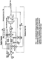
- FIG. 2 shows in block diagram form an embodiment of a linear digitally predistorted PA.
- DPD estimator block In the DPD estimator block, a least square algorithm is utilized to find the DPD coefficients, and then transfer them to DPD block.
- the detailed DPD algorithm is shown in Figure 4 .
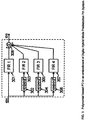
- FIG. 3 is a block diagram showing a predistortion (PD) part in the DHMPA system of the present invention.
- the PD in the present invention generally utilizes an adaptive polynomial-based digital predistortion system.
- Another embodiment of the PD utilizes a LUT-based digital predistortion system.
- the PD illustrated in FIG. 3 and in embodiments disclosed in FIG. 7 and FIG. 8 , discussed below, are processed in the digital processor by an adaptive algorithm, presented in U.S. Patent application S.N. 11/961,969 , entitled A Method for Baseband Predistortion Linearization in Multi-Channel Wideband Communication Systems.
- FIR finite impulse response
- the PD also contains the third order product generation block 302, the fifth order product generation block 304, and the seventh order product generation block 306.
- the output signals from FIR filters are combined in the summation block 308. Coefficients for multiple FIR filters are updated by the digital predistortion algorithm.
- the DPD estimator compares x(n) and its corresponding feedback signal y(n- ⁇ d) to find the DPD coefficients, where ⁇ d is the delay of the feedback path. As the feedback path delay is different for each PA, this delay should be identified before the signal arrives at the coefficient estimation.
- the amplitude difference correlation function of the transmission, x(n), and feedback data, y(n) is applied to find the feedback path delay.
- the delay n that maximizes the correlation C(m) is the feedback path delay.
- the delay estimation block is shown in Figure 5 .
- fractional delay estimation is necessary. To simplify the design, only a half-sample delay is considered in this design, as shown in Figure 6 . It will be appreciated that smaller fractional delays can also be utilized in at least some embodiments.
- an upsampling approach is the common choice, but in this design, in order to avoid a very high sampling frequency in the FPGA, an interpolation method is used to get the half-sample delay data.
- the data with integer delay and fractional delay are transferred in parallel.
- the fractional delay path or the integer delay path will be chosen is decided by the result of the amplitude difference correlator. If the correlation result is odd, the integer path will be chosen, otherwise the fractional delay path will be chosen.
- Phase offset between the transmission signal and the feedback signal exists in the circuit. For a better and faster convergence of the DPD coefficient estimation, this phase offset should be removed.
- N is chosen to be 4096. The choice of N will depend on the desired accuracy.
- h k x(n - i)
- w k a ij
- k (i - 1)N + j.
- QR-RLS algorithm (Haykin, 1996) is implemented to solve this problem.
- QR_RLS algorithm ⁇ d i ⁇ y i ⁇ h i w ⁇ w ⁇ i ⁇ w i ⁇ w ⁇ q i ⁇ ⁇ i / 2 * w i ⁇ w ⁇ where ⁇ i is a diagonal matrix, and q i is a vector.
- a block of data (in this design, there are 4096 data in one block) is stored in memory, and the algorithm uses all the data in memory to estimate the DPD coefficient.
- the DPD coefficients are only updated after one block of data is processed. The matrix A will be used for the next iteration process, which will make the convergence faster.
- the DPD coefficient estimator calculates coefficients w i by using QR_RLS algorithm. These w i are copied to the DPD block to linearize the PA.
- Figures 7 and 8 are block diagrams showing more sophisticated embodiments of DHMPA system, where like elements are indicated with like numerals and elements not numbered in Figure 8 have the same reference numerals as shown in Figure 7 .
- the embodiments of Figures 7 and 8 apply crest factor reduction (CFR) prior to the PD with an adaptation algorithm in one digital processor, so as to reduce the PAPR, EVM and ACPR and compensate the memory effects and variation of the linearity due to the temperature changing of the PA.
- CFR crest factor reduction
- the digital processor can take nearly any form; for convenience, an FPGA implementation is shown as an example, but a general purpose processor is also acceptable in many embodiments.
- the CFR implemented in the digital module of the embodiments is based on the scaled iterative pulse cancellation presented in patent application US61/041,164, filed March 31, 2008 , entitled An Efficient Peak Cancellation Method For Reducing The Peak-To-Average Power Ratio In Wideband Communication Systems, incorporated herein by reference.
- the CFR is included to enhance performance and hence optional.
- the CFR can be removed from the embodiments without affecting the overall functionality.
- FIG. 7 is a block diagram showing a DHMPA system implemented with DQM in accordance with an embodiment of the present invention.
- the system shown in Figure 7 has a dual mode of RF-in 700 and/or multi-carrier digital signal 705 at the input, and an RF signal at the output 710.
- the dual mode of signal input allows maximum flexibility: RF-in (the "RF-in Mode") or baseband digital-in (the "Baseband-in Mode”).
- the system shown in Figure 7 comprises three key portions: a reconfigurable digital (hereinafter referred as "FPGA-based Digital") module 715, a power amplifier module 760 and a feedback path 725.
- FPGA-based Digital reconfigurable digital
- the FPGA-based Digital part comprises a digital processor 715 (e.g. FPGA), digital-to-analog converters 735 (DACs), analog-to-digital converters 740 (ADCs), and a phase-locked loop (PLL) 745. Since the embodiment of Figure 7 has a dual input mode, the digital processor has two paths of signal processing. For the RF signal input path, the digital processor has implemented a digital quadrature demodulator (DQDM), a CFR, a PD, and a digital quadrature modulator (DQM). For the baseband digital input path, a digital up-converter (DUC), CFR, PD, and a DQM are implemented.
- DQDM digital quadrature demodulator
- CFR digital quadrature demodulator
- PD digital quadrature modulator
- DQM digital quadrature modulator
- the RF-in Mode of the embodiment shown in Figure 7 has implemented a down converter (DNC) 750 prior to the FPGA-based Digital part and an ADC 740 prior to the FPGA.
- An analog down converted signal is provided to the FPGA-based Digital module and converted to a digital signal by the ADC 740.
- the digitally converted signal is demodulated by the DQDM to generate both real and imaginary signals and then PAPR of the signal is reduced by CFR.
- the peak reduced signal is predistorted to linearize the amplifier and is passed through a DQM to generate the real signal and then converted to an intermediate frequency (IF) analog signal by a DAC in the FPGA-based Digital part.
- IF intermediate frequency
- the Baseband-in Mode of the system of Figure 7 works slightly differently from the RF-in Mode. Digital data streams from multi-channels as I-Q signals are coming to the FPGA-based Digital module and are digitally up-converted to digital IF signals by the DUC. From this point onwards, the Baseband-in Mode and RF-in Mode proceeds identically. These IF signals are then passed through the CFR block so as to reduce the signal's PAPR. This PAPR suppressed signal is digitally predistorted in order to pre-compensate for nonlinear distortions of the power amplifier.
- the memory effects due to self-heating, bias networks, and frequency dependencies of the active device are compensated by the adaptation algorithm in the PD, as well.
- the coefficients of the PD are adapted by a synchronizing the wideband captured output signal from the feedback path 725 with the reference signal.
- the digital predistortion algorithm performs the synchronization and compensation..
- the predistorted signal is passed through a DQM in order to generate the real signal and then converted to an IF analog signal by the DAC 740 as shown.
- the DQM is not required to be implemented in the FPGA, or at all, in all embodiments.
- the AQM Implementation can be implemented with two DACs to generate real and imaginary signals, respectively.
- the gate bias voltage 753 of the power amplifier is determined by the adaptation algorithm and then adjusted through the DACs 535 in order to stabilize the linearity fluctuations due to the temperature changes in the power amplifier..
- the power amplifier part comprises a UPC for a real signal (such as illustrated in the embodiment shown in Figures 7 ), or an AQM for real and complex signals (such as the embodiment of a DHMPA system depicted in Figure 8 ) from the FPGA-based Digital module, a high power amplifier with multi-stage drive amplifiers, and a temperature sensor.
- efficiency boosting techniques such as Doherty, Envelope Elimination and Restoration (EER), Envelope Tracking (ET), Envelope Following (EF), and Linear amplification using Nonlinear Components (LINC) can be used, depending upon the embodiment.
- EER Envelope Elimination and Restoration
- Envelope Tracking Envelope Tracking
- EF Envelope Following
- LINC Linear amplification using Nonlinear Components
- the feedback portion comprises a directional coupler, a mixer, a gain amplifier, a band pass filter (BPF), and a Digital to Analog Converter (DAC).
- these analog components can be mixed and matched with other analog components.
- Part of the RF output signal of the amplifier is sampled by the directional coupler and then down converted to an IF analog signal by the local oscillation signal in the mixer.
- the IF analog signal is passing through the the gain amplifier, and the BPF (e.g., surface acoustic wave filter) which can capture the out-of-band distortions.
- BPF e.g., surface acoustic wave filter
- the output of the BPF is provided to the ADC of the FPGA-based Digital module in order to determine the dynamic parameters of the digital PD depending on output power levels and asymmetrical distortions due to the memory effects.
- temperature is also detected by the detector 580 to calculate the variation of linearity and then adjust gate bias voltage of the PA. More details of the PD algorithm and self-adaptation feedback algorithm can be appreciated from Figure 3 , discussed above, which shows a polynomial-based predistortion algorithm and from Figure 4 , also discussed above, which shows the block diagram of the digital predistorter synchronization algorithm which can be used in some embodiments of the invention.
- the CFR in the FPGA-based Digital part is only able to achieve a small reduction of the PAPR in order to meet the strict EVM specification. In general circumstances, this means the CFR's power efficiency enhancement capability is limited.
- a novel technique is included to compensate the in-band distortions from CFR by use of a "Clipping Error Restoration Path" 790, hence maximizing the DHMPA system power efficiency in those strict EVM environments.
- the Clipping Error Restoration Path has an additional DAC 735 in the FPGA-based Digital portion and an extra UPC 720 in the power amplifier part (see Figures 7 and 8 ).
- the Clipping Error Restoration Path can allow compensation of in-band distortions resulting from the CFR at the output of the power amplifier. Further, any delay mismatch between the main path and the Clipping Error Restoration Path can be aligned using digital delay in the FPGA.
- the RF input signal is first down-converted to baseband digital signals, and then digitally up-converted to digital IF signals (-7.5 MHz, -2.5 MHz, 2.5 MHz, 7.5 MHz). If the system of Figure 7 has a Baseband-in Mode, then the digital data streams from multi-channels are digitally up-converted to digital IF signals (-7.5 MHz, -2.5 MHz, 2.5 MHz, 7.5 MHz) directly as they enter the digital processor. The CFR then reduces the PAPR. The peak-reduced signal is predistorted to linearize the DPA and is passing through two DACs for real and imaginary signals and finally through an AQM.
- FIG. 9 is a block diagram showing an embodiment of the analog quadrature modulator compensation structure.
- the input signal is separated into an in-phase component X I and a quadrature component X Q .
- the analog quadrature modulator compensation structure comprises four real filters ⁇ g11, g12, g21, g22 ⁇ and two DC offset compensation parameters c1, c2.
- the DC offsets in the AQM will be compensated by the parameters c1, c2.
- the frequency dependence of the AQM will be compensated by the filters ⁇ g11, g12, g21, g22 ⁇ .
- the order of the real filters is dependent on the level of compensation required.
- the output signals YI and YQ will be presented to the AQM's in-phase and quadrature ports.
- the DNC frequency translates the RF signal into a low IF signal.
- the IF signal is then presented to the ADC whereupon it is digitally down-converted to baseband followed by CFR and predistortion (PD).
- the output of the PD is a baseband signal which will then be digitally upconverted to an IF frequency and presented to the DAC.
- the output of the DAC is then further frequency translated to a RF frequency through the up-converter (UPC.)
- UPC up-converter
- the DHMPA system of the present invention enhances efficiency and linearity relative to the prior art since the DHMPA system is able to implement CFR, DPD and adaptation algorithms in one digital processor, which consequently saves hardware resources and processing time.
- the DHMPA system is also reconfigurable and field-programmable since the algorithms and power-efficiency-enhancing features can be adjusted like software in the digital processor at anytime.
- the DHMPA system accepts RF modulated signal as input, it is not necessary to use coded I and Q channel signals in the baseband. Therefore, the performance of wireless base-station systems can be enhanced simply by replacing the existing PA modules with the DHMPA. The result is that the present invention provides a "plug and play" PA system solution such that the structure of existing base-station systems does not need to be modified or rebuilt for a new set of signal channels in order to benefit from high efficiency and high linearity PA system performance.
- the DHMPA system is agnostic to modulation schemes such as quadrature phase shift keying (QPSK), quadrature amplitude modulation (QAM), Orthogonal Frequency Division Multiplexing (OFDM), etc. in code division multiple access (CDMA), global system for wireless communications (GSM), WCDMA, CDMA2000, and wireless LAN systems.
- QPSK quadrature phase shift keying
- QAM quadrature amplitude modulation
- OFDM Orthogonal Frequency Division Multiplexing
- CDMA code division multiple access
- GSM global system for wireless communications
- WCDMA CDMA2000
- wireless LAN systems wireless local area network
- Other benefits of the DHMPA system of the present invention include correction of PA non-linearities in repeater or indoor coverage systems that do not have the necessary baseband signals information readily available.
Landscapes
- Engineering & Computer Science (AREA)
- Power Engineering (AREA)
- Signal Processing (AREA)
- Physics & Mathematics (AREA)
- Computer Networks & Wireless Communication (AREA)
- Nonlinear Science (AREA)
- General Physics & Mathematics (AREA)
- Mathematical Analysis (AREA)
- Mathematical Optimization (AREA)
- Pure & Applied Mathematics (AREA)
- Algebra (AREA)
- Amplifiers (AREA)
- Transmitters (AREA)
Description
- This application claims the benefit of
U.S. Patent Application Ser. No. 61/288,844, filed Dec. 21, 2009 - The present invention generally relates to wireless communication systems using complex modulation techniques. More specifically, the present invention relates to power amplifier systems for wireless communications.
- A wideband mobile communication system using complex modulation techniques, such as wideband code division multiple access (WCDMA) and orthogonal frequency division multiplexing (OFDM), has large peak-to-average power ratio (PAPR) specifications and hence requires highly linear power amplifiers for its RF transmissions. The conventional feedforward linear power amplifier (FFLPA) has been widely utilized due to its excellent linearity performance in spite of poor power efficiency.
- Conventional FFLPAs are mainly based on the principle of error subtraction and power-matching with dedicated hardware circuitries to realize non-linear corrections to PA. These approaches must use an auxiliary PA and complicated hardware circuitries to match exactly the transmitted power-balance, time-delay and errors generated by the main PA. After a perfect matching is obtained, the non-linear distortion errors from the main PA can then be canceled by those distortion errors from the auxiliary PA. Due to the complexities of the nonlinear predistortion circuits, which among other things involve many variables and parameters, FFLPAs require significant fine tuning and other calibration efforts. In addition, such traditional FFLPA schemes are also vulnerable to fluctuating environmental conditions, such as temperature and humidity changes, since perfect alignment of the main PA's signal and that of the auxiliary PA are vital. As a result, traditional predistortion schemes are costly to implement and are limited in their predistortion accuracy and stability in a commercial wireless system environment.
- In order to overcome the FFLPA's poor efficiency, digital baseband predistortion (PD) has been demonstrated due to the recent advances in digital signal processing (DSP) technology. In addition, Doherty power amplifiers (DPA) have also been applied to these linearization systems to improve power efficiency. However, there is still a demand for higher performance of the power amplifier such as more linearity and better efficiency with less expensive architecture.
- Conventional DSP-based PD schemes utilize digital microprocessors to compute, calculate and correct the PA's nonlinearities, typically by performing fast tracking and adjustments of signals in the PA system. However, conventional DSP-based PD schemes are challenged by variations of the linearity performance of the amplifier due to changes in the environment such as temperature and the asymmetric distortions of the output signal of the PA resulting from memory effects. All of these variations and distortions have to be compensated for. Conventional PD algorithms are based on a wideband feedback signal, and require a high speed analog-to-digital converter (ADC) in order to capture the necessary information. In addition, time-synchronizations are typically required to capture an error signal between a reference signal and a distorted signal. This time-matching process may result in small synchronization errors which can further affect conventional PD schemes' linearization performance. Amplitude and phase synchronization is also required in order to align the reference signal and the distorted signal.
- Moreover, conventional PD schemes necessitate coded in-phase (I) and quadrature (Q) channel signals in the baseband as the required ideal or reference signals. As a result, conventional PD schemes are often standard or modulation specific and must be closely tailored to each baseband system. Therefore, in order to deploy conventional PD schemes into base-stations, the PD engines must be embedded into the baseband architecture of base-stations. This embodiment is a practical implementation challenge since it is frequently inconvenient or impossible to modify the baseband architectures of existing base-stations or base-station designs. Once the PD scheme is set up for a specific base-station design, it is often not reconfigurable and hence not upgradeable to future changes in standards or modulations. Furthermore, since traditional PD approaches require baseband I-Q signal sources to operate, they are inapplicable to certain RF systems that do not possess any baseband I-Q signal sources, such as repeater and indoor signal coverage sub-systems.
- Accordingly, the present invention has been made in view of the above problems, and it is an object of the present invention to provide a high performance and cost effective method of power amplifier systems with high linearity and high efficiency for wideband communication system applications. The above object is solved by the combination of features of
independent claim 1. Preferred embodiments are defined in the dependent claims. The present disclosure provides a field-reconfigurable power amplifier system that supports multi-modulation schemes (modulation agnostic), multi-carriers and multi-channels. In multi-channel configurations of the present invention there can be more than one PA for multiple bands. - To achieve the above objects, the present invention is generally based on the method of adaptive digital predistortion to linearize a power amplifier in the RF domain. Various embodiments of the invention are disclosed. In an embodiment, the combination of crest factor reduction, PD, power efficiency boosting techniques as well as coefficient adaptive algorithms are utilized within a PA system. In another embodiment, analog quadrature modulator compensation structure is also utilized to enhance performance.
- Some embodiments of the present invention are able to monitor the fluctuation of the power amplifier characteristics and to self-adjust by means of a self-adaptation algorithm. One such self-adaptation algorithm presently disclosed is called a digital predistortion algorithm, which is implemented in the digital domain.
- Applications of the present invention are suitable for use with all wireless base-stations, access points, mobile equipment and wireless terminals, portable wireless devices, and other wireless communication systems such as microwave and satellite communications.
- A RF-digital hybrid mode power amplifier system for achieving high efficiency and high linearity in wideband communication systems is disclosed. The present invention is based on the method of adaptive digital predistortion to linearize a power amplifier in the RF domain. The power amplifier characteristics such as variation of linearity and asymmetric distortion of the amplifier output signal are sampled in a feedback path and controlled by the adaptation algorithm in a digital module. Therefore, in an embodiment, the present invention is capable of compensating for the nonlinearities as well as memory effects of power amplifier systems and also improves performance, in terms of power added efficiency, adjacent channel leakage ratio (ACLR) and peak-to-average power ratio. The present disclosure enables a power amplifier system to be field reconfigurable and support multi-modulation schemes (modulation agnostic), multi-carriers and multi-channels. As a result, the digital hybrid mode power amplifier system is particularly suitable for wireless transmission systems, such as base-stations, repeaters, and indoor signal coverage systems, where baseband I-Q signal information is not readily available.
- Further objects and advantages of the present invention can be more fully understood from the following detailed description taken in conjunction with the accompanying drawings in which:
-
Figure 1 is a block diagram showing the basic form of a digital hybrid mode power amplifier system. -
Figure 2 is a block diagram showing a simple digital predistortion block diagram for a power amplifier system according to one embodiment of the present invention. -
Figure 3 is a block diagram showing polynomial-based predistortion in a digital hybrid mode power amplifier system of the present invention. -
Figure 4 is a block diagram of the digital predistortion algorithm applied for self-adaptation in a digital hybrid mode power amplifier system of the present invention. -
Figure 5 is a delay estimation block diagram of the present invention. -
Figure 6 is a block diagram of a fractional delay for the present invention. -
Figure 7 is a block diagram showing a digital hybrid mode power amplifier system implemented with a down converter (DNC) and UPC-based clipping error restoration path according to another embodiment of the present invention.. -
Figure 8 is a block diagram showing a digital hybrid mode power amplifier system implemented with a DNC and an analog quadrature modulator (AQM) according to another embodiment of the present invention. -
Figure 9 is a block diagram showing an embodiment of the analog quadrature modulator compensation structure. - The acronyms used herein have the following meanings:
- ACLR
- Adjacent Channel Leakage Ratio
- ACPR
- Adjacent Channel Power Ratio
- ADC
- Analog to Digital Converter
- AQDM
- Analog Quadrature Demodulator
- AQM
- Analog Quadrature Modulator
- AQDMC
- Analog Quadrature Demodulator Corrector
- AQMC
- Analog Quadrature Modulator Corrector
- BPF
- Bandpass Filter
- CDMA
- Code Division Multiple Access
- CFR
- Crest Factor Reduction
- DAC
- Digital to Analog Converter
- DET
- Detector
- DHMPA
- Digital Hybrid Mode Power Amplifier
- DDC
- Digital Down Converter
- DNC
- Down Converter
- DPA
- Doherty Power Amplifier
- DQDM
- Digital Quadrature Demodulator
- DQM
- Digital Quadrature Modulator
- DSP
- Digital Signal Processing
- DUC
- Digital Up Converter
- EER
- Envelope Elimination and Restoration
- EF
- Envelope Following
- ET
- Envelope Tracking
- EVM
- Error Vector Magnitude
- FFLPA
- Feedforward Linear Power Amplifier
- FIR
- Finite Impulse Response
- FPGA
- Field-Programmable Gate Array
- GSM
- Global System for Mobile communications
- I-Q
- In-phase / Quadrature
- IF
- Intermediate Frequency
- LINC
- Linear Amplification using Nonlinear Components
- LO
- Local Oscillator
- LPF
- Low Pass Filter
- MCPA
- Multi-Carrier Power Amplifier
- MDS
- Multi-Directional Search
- OFDM
- Orthogonal Frequency Division Multiplexing
- PA
- Power Amplifier
- PAPR
- Peak-to-Average Power Ratio
- PD
- Digital Baseband Predistortion
- PLL
- Phase Locked Loop
- QAM
- Quadrature Amplitude Modulation
- QPSK
- Quadrature Phase Shift Keying
- RF
- Radio Frequency
- SAW
- Surface Acoustic Wave Filter
- UMTS
- Universal Mobile Telecommunications System
- UPC
- Up Converter
- WCDMA
- Wideband Code Division Multiple Access
- WLAN
- Wireless Local Area Network
- The present invention is a novel RF-out PA system that utilizes an adaptive digital predistortion algorithm. The present invention is a hybrid system of digital and analog modules. The interplay of the digital and analog modules of the hybrid system both linearize the spectral regrowth and enhance the power efficiency of the PA while maintaining or increasing the wide bandwidth. The present invention, therefore, achieves higher efficiency and higher linearity for wideband complex modulation carriers.
-
FIG. 1 is a high level block diagram showing the basic system architecture which can be thought of, at least for some embodiments, as comprising digital and analog modules and a feedback path. The digital module is thedigital predistortion controller 101 which comprises the PD algorithm, other auxiliary DSP algorithms, and related digital circuitries. The analog module is themain power amplifier 102, other auxiliary analog circuitries such as DPA, and related peripheral analog circuitries of the overall system. The present invention is a "black box", plug-and-play type system because it accepts RF modulatedsignal 100 as its input, and provides a substantially identical but amplified RF signal 103 as its output, therefore, it is RF-in/RF-out. Baseband input signals can be applied directly to the Digital Predistorter Controller according to one embodiment of the present invention. An Optical input signal can be applied directly to the Digital Predistorter Controller according to one embodiment of the present invention. The feedback path essentially provides a representation of the output signal to thepredistortion controller 101. The present invention is sometimes referred to as a digital hybrid mode power amplifier (DHMPA) system hereinafter. - Digital Predistortion (DPD) is a technique to linearize a power amplifier (PA).
FIG. 2 shows in block diagram form an embodiment of a linear digitally predistorted PA. In the DPD block, a memory polynomial model is used as the predistortion function (FIG. 3 ), and complies with the formula:
- In the DPD estimator block, a least square algorithm is utilized to find the DPD coefficients, and then transfer them to DPD block. The detailed DPD algorithm is shown in
Figure 4 . -
Figure 3 is a block diagram showing a predistortion (PD) part in the DHMPA system of the present invention. The PD in the present invention generally utilizes an adaptive polynomial-based digital predistortion system. Another embodiment of the PD utilizes a LUT-based digital predistortion system. More specifically, the PD illustrated inFIG. 3 and in embodiments disclosed inFIG. 7 andFIG. 8 , discussed below, are processed in the digital processor by an adaptive algorithm, presented inU.S. Patent application S.N. 11/961,969 , entitled A Method for Baseband Predistortion Linearization in Multi-Channel Wideband Communication Systems. The PD for the DHMPA system inFIG. 3 has multiple finite impulse response (FIR) filters, that is,FIR1 301,FIR2 303,FIR3 305, andFIR4 307. The PD also contains the third orderproduct generation block 302, the fifth orderproduct generation block 304, and the seventh orderproduct generation block 306. The output signals from FIR filters are combined in thesummation block 308. Coefficients for multiple FIR filters are updated by the digital predistortion algorithm. - The DPD estimator compares x(n) and its corresponding feedback signal y(n-Δd) to find the DPD coefficients, where Δd is the delay of the feedback path. As the feedback path delay is different for each PA, this delay should be identified before the signal arrives at the coefficient estimation. In this design, the amplitude difference correlation function of the transmission, x(n), and feedback data, y(n), is applied to find the feedback path delay. The correlation is given by

Figure 5 . - Since the feedback path goes through analog circuitry, the delay between the transmission and feedback path could be a fractional sample delay. To synchronize the signals more accurately, fractional delay estimation is necessary. To simplify the design, only a half-sample delay is considered in this design, as shown in
Figure 6 . It will be appreciated that smaller fractional delays can also be utilized in at least some embodiments. - To get the half-sample delay data, an upsampling approach is the common choice, but in this design, in order to avoid a very high sampling frequency in the FPGA, an interpolation method is used to get the half-sample delay data. The data with integer delay and fractional delay are transferred in parallel. The interpolation function for fractional delay is

- Whether the fractional delay path or the integer delay path will be chosen is decided by the result of the amplitude difference correlator. If the correlation result is odd, the integer path will be chosen, otherwise the fractional delay path will be chosen.
- Phase offset between the transmission signal and the feedback signal exists in the circuit. For a better and faster convergence of the DPD coefficient estimation, this phase offset should be removed.
- The transmission signal x(n) and feedback signal y(n) can be expressed as

x -θy ) can be calculated through


- As the gain of the PA may change slightly, the feedback gain should be corrected to avoid the error from the gain mismatch. The feedback signal is corrected according to the function

- The least square solution for DPD coefficient estimation is formulated as


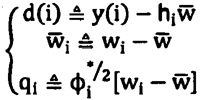
The QR_RLS algorithm gets the ith moment φi and qi from its (i - 1)th moment through a unitary transformation:
- To apply QR_RLS algorithm more efficiently in FPGA, a squared-root-free Givens rotation is applied for the unitary transformation process (E.N. Frantzeskakis, 1994)


- For RLS algorithm, the ith moment is achieved as below:


- In the iterative process, a block of data (in this design, there are 4096 data in one block) is stored in memory, and the algorithm uses all the data in memory to estimate the DPD coefficient. In order to make the DPD performance more stable, the DPD coefficients are only updated after one block of data is processed. The matrix A will be used for the next iteration process, which will make the convergence faster.
- To make sure the performance of the DPD is stable, a weighting factor f is used when updating the DPD coefficients as

- The DPD coefficient estimator calculates coefficients wi by using QR_RLS algorithm. These wi are copied to the DPD block to linearize the PA.
-
Figures 7 and8 are block diagrams showing more sophisticated embodiments of DHMPA system, where like elements are indicated with like numerals and elements not numbered inFigure 8 have the same reference numerals as shown inFigure 7 . The embodiments ofFigures 7 and8 apply crest factor reduction (CFR) prior to the PD with an adaptation algorithm in one digital processor, so as to reduce the PAPR, EVM and ACPR and compensate the memory effects and variation of the linearity due to the temperature changing of the PA. The digital processor can take nearly any form; for convenience, an FPGA implementation is shown as an example, but a general purpose processor is also acceptable in many embodiments. The CFR implemented in the digital module of the embodiments is based on the scaled iterative pulse cancellation presented in patent applicationUS61/041,164, filed March 31, 2008 -
Figure 7 is a block diagram showing a DHMPA system implemented with DQM in accordance with an embodiment of the present invention. The system shown inFigure 7 has a dual mode of RF-in 700 and/or multi-carrierdigital signal 705 at the input, and an RF signal at theoutput 710. The dual mode of signal input allows maximum flexibility: RF-in (the "RF-in Mode") or baseband digital-in (the "Baseband-in Mode"). The system shown inFigure 7 comprises three key portions: a reconfigurable digital (hereinafter referred as "FPGA-based Digital")module 715, apower amplifier module 760 and afeedback path 725. - The FPGA-based Digital part comprises a digital processor 715 (e.g. FPGA), digital-to-analog converters 735 (DACs), analog-to-digital converters 740 (ADCs), and a phase-locked loop (PLL) 745. Since the embodiment of
Figure 7 has a dual input mode, the digital processor has two paths of signal processing. For the RF signal input path, the digital processor has implemented a digital quadrature demodulator (DQDM), a CFR, a PD, and a digital quadrature modulator (DQM). For the baseband digital input path, a digital up-converter (DUC), CFR, PD, and a DQM are implemented. - The RF-in Mode of the embodiment shown in
Figure 7 has implemented a down converter (DNC) 750 prior to the FPGA-based Digital part and anADC 740 prior to the FPGA. An analog down converted signal is provided to the FPGA-based Digital module and converted to a digital signal by theADC 740. The digitally converted signal is demodulated by the DQDM to generate both real and imaginary signals and then PAPR of the signal is reduced by CFR. The peak reduced signal is predistorted to linearize the amplifier and is passed through a DQM to generate the real signal and then converted to an intermediate frequency (IF) analog signal by a DAC in the FPGA-based Digital part. However, it is not required in all embodiments to implement DQDM and DQM in the FPGA. If, as shown inFigures 7 and8 , a digital modulator will not be used, then two DAC's 801 behind the FPGA feedingAQM module 800 can be used to generate real and imaginary signals, respectively (the "AQM Implementation"). - The Baseband-in Mode of the system of
Figure 7 works slightly differently from the RF-in Mode. Digital data streams from multi-channels as I-Q signals are coming to the FPGA-based Digital module and are digitally up-converted to digital IF signals by the DUC. From this point onwards, the Baseband-in Mode and RF-in Mode proceeds identically. These IF signals are then passed through the CFR block so as to reduce the signal's PAPR. This PAPR suppressed signal is digitally predistorted in order to pre-compensate for nonlinear distortions of the power amplifier. - In either input mode, the memory effects due to self-heating, bias networks, and frequency dependencies of the active device are compensated by the adaptation algorithm in the PD, as well. The coefficients of the PD are adapted by a synchronizing the wideband captured output signal from the
feedback path 725 with the reference signal. The digital predistortion algorithm performs the synchronization and compensation.. The predistorted signal is passed through a DQM in order to generate the real signal and then converted to an IF analog signal by theDAC 740 as shown. As disclosed above, the DQM is not required to be implemented in the FPGA, or at all, in all embodiments. Alternatively, if the DQM is not used in the FPGA, then the AQM Implementation can be implemented with two DACs to generate real and imaginary signals, respectively. Thegate bias voltage 753 of the power amplifier is determined by the adaptation algorithm and then adjusted through the DACs 535 in order to stabilize the linearity fluctuations due to the temperature changes in the power amplifier.. - The power amplifier part comprises a UPC for a real signal (such as illustrated in the embodiment shown in
Figures 7 ), or an AQM for real and complex signals (such as the embodiment of a DHMPA system depicted inFigure 8 ) from the FPGA-based Digital module, a high power amplifier with multi-stage drive amplifiers, and a temperature sensor. In order to improve the efficiency performance of the DHMPA system, efficiency boosting techniques such as Doherty, Envelope Elimination and Restoration (EER), Envelope Tracking (ET), Envelope Following (EF), and Linear amplification using Nonlinear Components (LINC) can be used, depending upon the embodiment. These power efficiency techniques can be mixed and matched and are optional features to the fundamental DHMPA system. One such Doherty power amplifier technique is presented in commonly assignedU.S. Provisional Patent Application S.N. 60/925,577, filed April 23, 2007 U.S. Patent Application S.N. 12/603,419, filed 10/21/2009 - The feedback portion comprises a directional coupler, a mixer, a gain amplifier, a band pass filter (BPF), and a Digital to Analog Converter (DAC). Depending upon the embodiment, these analog components can be mixed and matched with other analog components. Part of the RF output signal of the amplifier is sampled by the directional coupler and then down converted to an IF analog signal by the local oscillation signal in the mixer. The IF analog signal is passing through the the gain amplifier, and the BPF (e.g., surface acoustic wave filter) which can capture the out-of-band distortions. The output of the BPF is provided to the ADC of the FPGA-based Digital module in order to determine the dynamic parameters of the digital PD depending on output power levels and asymmetrical distortions due to the memory effects. In addition, temperature is also detected by the detector 580 to calculate the variation of linearity and then adjust gate bias voltage of the PA. More details of the PD algorithm and self-adaptation feedback algorithm can be appreciated from
Figure 3 , discussed above, which shows a polynomial-based predistortion algorithm and fromFigure 4 , also discussed above, which shows the block diagram of the digital predistorter synchronization algorithm which can be used in some embodiments of the invention. - In the case of a strict EVM requirement for broadband wireless access such as WiMAX or other OFDM based schemes (EVM < 2.5%), the CFR in the FPGA-based Digital part is only able to achieve a small reduction of the PAPR in order to meet the strict EVM specification. In general circumstances, this means the CFR's power efficiency enhancement capability is limited. In some embodiments of the present invention, a novel technique is included to compensate the in-band distortions from CFR by use of a "Clipping Error Restoration Path" 790, hence maximizing the DHMPA system power efficiency in those strict EVM environments. As noted above, the Clipping Error Restoration Path has an
additional DAC 735 in the FPGA-based Digital portion and anextra UPC 720 in the power amplifier part (seeFigures 7 and8 ). The Clipping Error Restoration Path can allow compensation of in-band distortions resulting from the CFR at the output of the power amplifier. Further, any delay mismatch between the main path and the Clipping Error Restoration Path can be aligned using digital delay in the FPGA. - Referring again to
Figure 7 , the RF input signal is first down-converted to baseband digital signals, and then digitally up-converted to digital IF signals (-7.5 MHz, -2.5 MHz, 2.5 MHz, 7.5 MHz). If the system ofFigure 7 has a Baseband-in Mode, then the digital data streams from multi-channels are digitally up-converted to digital IF signals (-7.5 MHz, -2.5 MHz, 2.5 MHz, 7.5 MHz) directly as they enter the digital processor. The CFR then reduces the PAPR. The peak-reduced signal is predistorted to linearize the DPA and is passing through two DACs for real and imaginary signals and finally through an AQM. -
FIG. 9 . is a block diagram showing an embodiment of the analog quadrature modulator compensation structure. The input signal is separated into an in-phase component XI and a quadrature component XQ. The analog quadrature modulator compensation structure comprises four real filters {g11, g12, g21, g22} and two DC offset compensation parameters c1, c2. The DC offsets in the AQM will be compensated by the parameters c1, c2. The frequency dependence of the AQM will be compensated by the filters {g11, g12, g21, g22}. The order of the real filters is dependent on the level of compensation required. The output signals YI and YQ will be presented to the AQM's in-phase and quadrature ports. - The configuration of the power amplifier part and the feedback part of the system shown in
Figure 8 are the same as for the system shown inFIG. 7 . - In the system shown in
Figure 8 , the DNC frequency translates the RF signal into a low IF signal. The IF signal is then presented to the ADC whereupon it is digitally down-converted to baseband followed by CFR and predistortion (PD). The output of the PD is a baseband signal which will then be digitally upconverted to an IF frequency and presented to the DAC. The output of the DAC is then further frequency translated to a RF frequency through the up-converter (UPC.) The configuration of the power amplifier part and the feedback part of system ofFigure 8 are the same as for theFIG. 7 System. - In summary, the DHMPA system of the present invention enhances efficiency and linearity relative to the prior art since the DHMPA system is able to implement CFR, DPD and adaptation algorithms in one digital processor, which consequently saves hardware resources and processing time. The DHMPA system is also reconfigurable and field-programmable since the algorithms and power-efficiency-enhancing features can be adjusted like software in the digital processor at anytime.
- Furthermore, since the DHMPA system accepts RF modulated signal as input, it is not necessary to use coded I and Q channel signals in the baseband. Therefore, the performance of wireless base-station systems can be enhanced simply by replacing the existing PA modules with the DHMPA. The result is that the present invention provides a "plug and play" PA system solution such that the structure of existing base-station systems does not need to be modified or rebuilt for a new set of signal channels in order to benefit from high efficiency and high linearity PA system performance.
- Moreover, the DHMPA system is agnostic to modulation schemes such as quadrature phase shift keying (QPSK), quadrature amplitude modulation (QAM), Orthogonal Frequency Division Multiplexing (OFDM), etc. in code division multiple access (CDMA), global system for wireless communications (GSM), WCDMA, CDMA2000, and wireless LAN systems. This means that the DHMPA system is capable of supporting multi-modulation schemes, multi-carriers and multi-channels. Other benefits of the DHMPA system of the present invention include correction of PA non-linearities in repeater or indoor coverage systems that do not have the necessary baseband signals information readily available.
- Although the present invention has been described with reference to the preferred embodiments, it will be understood that the invention is not limited to the details described thereof. Various substitutions and modifications have been suggested in the foregoing description, and others will occur to those of ordinary skill in the art. Therefore, all such substitutions and modifications are intended to be embraced within the scope of the invention as defined in the appended claims.
Claims (6)
- A digital predistortion system for linearizing the output of power amplifiers comprising:input signal suitable for wireless communications,at least one power amplifier for outputting an amplified signal,at least one feedback signal derived from the amplified signal including a representation of a noise characteristic of the at least one power amplifier,estimator logic responsive to the at least one feedback signal for generating predistortion coefficients based at least in part on feedback path delay determined from the correlation given by the equation

 where x(n) represents transmission data, y(n) represents feedback data, c(m) is a correlation function, N is a number of data per block, m is a variable representing time, i is a counter for summation, and wherein a delay n that maximizes the correlation c(m) is the feedback path delay.
 - The digital predistortion system of claim 1 configured for base station applications further comprising a digital field programmable gate array that includes one or more of a digital up-converter, a crest factor reduction, a predistorter, or a digital quadrature modulator.
- The digital predistortion system of claim 1 configured for repeater applications further comprising a digital field programmable gate array that includes at least one of a digital quadrature demodulator, a crest factor reduction, a predistorter, or a digital quadrature modulator.
- The digital predistortion system of claim 1 further comprising a digital field programmable gate array that provides predistortion that compensates adaptively for both nonlinearity and memory effects by generating asymmetric distortion of the power amplifier.
- The digital predistortion system of claim 1 further comprising a digital field programmable gate array that includes an adaptation algorithm to determine the optimum gate bias voltage of the power amplifier for stabilizing the linearity fluctuations due to the temperature changes of the power amplifier.
- The digital predistortion system of claim 1 wherein the power amplifier portion uses at least one of the following efficiency boosting techniques: Doherty, Envelope Elimination and Restoration, Envelope Tracking, Envelope Following, or Linear amplification using Nonlinear Components in order to maximize the efficiency of the power amplifier system.
Priority Applications (1)
| Application Number | Priority Date | Filing Date | Title |
|---|---|---|---|
| EP16166094.9A EP3068047A3 (en) | 2009-12-21 | 2010-12-21 | Modulation agnostic digital hybrid mode power amplifier system and method |
Applications Claiming Priority (5)
| Application Number | Priority Date | Filing Date | Title |
|---|---|---|---|
| US28883809P | 2009-12-21 | 2009-12-21 | |
| US28884709P | 2009-12-21 | 2009-12-21 | |
| US28884409P | 2009-12-21 | 2009-12-21 | |
| US28884009P | 2009-12-21 | 2009-12-21 | |
| PCT/IB2010/003449 WO2011077247A2 (en) | 2009-12-21 | 2010-12-21 | Modulation agnostic digital hybrid mode power amplifier system and method |
Related Child Applications (1)
| Application Number | Title | Priority Date | Filing Date |
|---|---|---|---|
| EP16166094.9A Division EP3068047A3 (en) | 2009-12-21 | 2010-12-21 | Modulation agnostic digital hybrid mode power amplifier system and method |
Publications (3)
| Publication Number | Publication Date |
|---|---|
| EP2517353A2 EP2517353A2 (en) | 2012-10-31 |
| EP2517353A4 EP2517353A4 (en) | 2014-11-19 |
| EP2517353B1 true EP2517353B1 (en) | 2016-04-20 |
Family
ID=44186772
Family Applications (4)
| Application Number | Title | Priority Date | Filing Date |
|---|---|---|---|
| EP16181745.7A Active EP3110231B1 (en) | 2009-12-21 | 2010-12-21 | High efficiency, remotely reconfigurable remote radio head unit system and method for wireless communications |
| EP16166094.9A Withdrawn EP3068047A3 (en) | 2009-12-21 | 2010-12-21 | Modulation agnostic digital hybrid mode power amplifier system and method |
| EP10848623.4A Active EP2524568B1 (en) | 2009-12-21 | 2010-12-21 | High efficiency, remotely reconfigurable remote radio head unit system and method for wireless communications |
| EP10838778.8A Active EP2517353B1 (en) | 2009-12-21 | 2010-12-21 | Modulation agnostic digital hybrid mode power amplifier system and method |
Family Applications Before (3)
| Application Number | Title | Priority Date | Filing Date |
|---|---|---|---|
| EP16181745.7A Active EP3110231B1 (en) | 2009-12-21 | 2010-12-21 | High efficiency, remotely reconfigurable remote radio head unit system and method for wireless communications |
| EP16166094.9A Withdrawn EP3068047A3 (en) | 2009-12-21 | 2010-12-21 | Modulation agnostic digital hybrid mode power amplifier system and method |
| EP10848623.4A Active EP2524568B1 (en) | 2009-12-21 | 2010-12-21 | High efficiency, remotely reconfigurable remote radio head unit system and method for wireless communications |
Country Status (6)
| Country | Link |
|---|---|
| US (6) | US8804870B2 (en) |
| EP (4) | EP3110231B1 (en) |
| JP (1) | JP5761646B2 (en) |
| KR (1) | KR101815329B1 (en) |
| CN (1) | CN102948071B (en) |
| WO (4) | WO2011098861A1 (en) |
Families Citing this family (140)
| Publication number | Priority date | Publication date | Assignee | Title |
|---|---|---|---|---|
| US8380143B2 (en) | 2002-05-01 | 2013-02-19 | Dali Systems Co. Ltd | Power amplifier time-delay invariant predistortion methods and apparatus |
| US8811917B2 (en) | 2002-05-01 | 2014-08-19 | Dali Systems Co. Ltd. | Digital hybrid mode power amplifier system |
| KR20100014339A (en) | 2006-12-26 | 2010-02-10 | 달리 시스템즈 씨오. 엘티디. | Method and system for baseband predistortion linearization in multi-channel wideband communication systems |
| US8238842B2 (en) * | 2009-03-03 | 2012-08-07 | Broadcom Corporation | Method and system for an on-chip and/or an on-package transmit/receive switch and antenna |
| EP3110231B1 (en) | 2009-12-21 | 2018-05-02 | Dali Systems Co. Ltd. | High efficiency, remotely reconfigurable remote radio head unit system and method for wireless communications |
| CN106160674A (en) * | 2009-12-21 | 2016-11-23 | 大力系统有限公司 | For improving the system of the isolation between transmitter and receiver |
| US8542768B2 (en) | 2009-12-21 | 2013-09-24 | Dali Systems Co. Ltd. | High efficiency, remotely reconfigurable remote radio head unit system and method for wireless communications |
| US8542766B2 (en) * | 2010-05-04 | 2013-09-24 | Samsung Electronics Co., Ltd. | Time alignment algorithm for transmitters with EER/ET amplifiers and others |
| US8600316B2 (en) * | 2010-06-28 | 2013-12-03 | Apple Inc. | Wireless circuits with minimized port counts |
| US8848766B2 (en) | 2010-08-17 | 2014-09-30 | Dali Systems Co. Ltd. | Neutral host architecture for a distributed antenna system |
| GB2483290B (en) | 2010-09-03 | 2015-07-22 | Nvidia Technology Uk Ltd | Transmitting a signal from a power amplifier |
| KR102136940B1 (en) | 2010-09-14 | 2020-07-23 | 달리 시스템즈 씨오. 엘티디. | Remotely Reconfigurable Distributed Antenna System and Methods |
| JP5236711B2 (en) * | 2010-09-30 | 2013-07-17 | 株式会社エヌ・ティ・ティ・ドコモ | Mobile communication terminal, multi-frequency simultaneous communication method |
| EP2630759B1 (en) | 2010-10-19 | 2019-03-20 | CommScope Technologies LLC | Systems and methods for transporting digital rf signals |
| US8432836B2 (en) * | 2010-11-09 | 2013-04-30 | Apple Inc. | Wireless circuitry with simultaneous voice and data capabilities and reduced intermodulation distortion |
| CN102625433B (en) * | 2011-01-31 | 2015-03-11 | 华为技术有限公司 | Carrier bearing method, apparatuses and radio remote unit |
| US8237500B1 (en) * | 2011-03-22 | 2012-08-07 | Sioma Edward M | Signal correction circuit for reducing errors and distortions and its associated method of operation |
| US8306484B1 (en) * | 2011-05-30 | 2012-11-06 | National Sun Yat-Sen University | Direct-conversion transmitter with resistance to local oscillator pulling effects |
| EP2719093B1 (en) * | 2011-06-13 | 2020-01-15 | LGC Wireless, LLC | Distributed antenna system architectures |
| WO2013009835A1 (en) | 2011-07-11 | 2013-01-17 | Andrew Llc | Method and apparatuses for managing a distributed antenna system |
| WO2013015646A2 (en) * | 2011-07-27 | 2013-01-31 | 엘지전자 주식회사 | Method and apparatus for transmitting synchronization signal in wireless communication system |
| WO2013033199A1 (en) | 2011-08-29 | 2013-03-07 | Andrew Llc | Configuring a distributed antenna system |
| CN102299878B (en) | 2011-09-06 | 2014-03-19 | 电信科学技术研究院 | Method and device for realizing multi-band digital predistortion (DPD) |
| US9628752B2 (en) | 2011-09-06 | 2017-04-18 | Comcast Cable Communications, Llc | Transmitting signals using directional diversity over a network |
| US8817859B2 (en) * | 2011-10-14 | 2014-08-26 | Fadhel Ghannouchi | Digital multi-band predistortion linearizer with nonlinear subsampling algorithm in the feedback loop |
| JP5375925B2 (en) * | 2011-11-01 | 2013-12-25 | 株式会社デンソー | Wireless communication device |
| BR112014010895B1 (en) | 2011-11-07 | 2022-06-14 | Dali Systems Co., Ltd | SYSTEM AND METHOD FOR MANAGING RESOURCE USE IN A DISTRIBUTED ANTENNA SYSTEM |
| CN103369727B (en) * | 2012-03-29 | 2016-06-22 | 中国移动通信集团公司 | A kind of radio frequency remote equipment, baseband processing equipment and data transmission method |
| GB2502045B (en) * | 2012-04-03 | 2015-03-25 | Nvidia Corp | Mitigating interference in wireless communication system |
| EP2654210B1 (en) * | 2012-04-16 | 2014-05-14 | Alcatel Lucent | Cross-talk cancellation in a multiband transceiver |
| US9236891B2 (en) | 2012-05-03 | 2016-01-12 | Telefonaktiebolaget L M Ericsson (Publ) | Radio communication transmitter apparatus and method |
| CN103457889B (en) * | 2012-05-31 | 2016-05-11 | 京信通信系统(中国)有限公司 | Data processing method, device and RRU based on multinuclear multi-channel radio remote unit RRU |
| CN103517391B (en) * | 2012-06-19 | 2017-05-24 | 京信通信技术(广州)有限公司 | Downlink signal sending method and radio remote unit |
| US9577954B2 (en) * | 2012-06-29 | 2017-02-21 | Cable Television Laboratories, Inc. | Time domain duplex (TDD) switching system |
| US9225296B2 (en) * | 2012-07-23 | 2015-12-29 | Dali Systems Co. Ltd. | Method and system for aligning signals widely spaced in frequency for wideband digital predistortion in wireless communication systems |
| EP2789107B1 (en) | 2012-08-09 | 2017-02-15 | Axell Wireless Ltd. | A digital capacity centric distributed antenna system |
| KR101941079B1 (en) | 2012-09-28 | 2019-01-23 | 삼성전자주식회사 | Appratus and method for correcting output characteristic in a power combiner |
| WO2014053149A1 (en) | 2012-10-05 | 2014-04-10 | Andrew Wireless Systems Gmbh | Capacity optimization sub-system for distributed antenna system |
| US8829993B2 (en) | 2012-10-30 | 2014-09-09 | Eta Devices, Inc. | Linearization circuits and methods for multilevel power amplifier systems |
| US9537456B2 (en) | 2012-10-30 | 2017-01-03 | Eta Devices, Inc. | Asymmetric multilevel backoff amplifier with radio-frequency splitter |
| US9166536B2 (en) | 2012-10-30 | 2015-10-20 | Eta Devices, Inc. | Transmitter architecture and related methods |
| CA2892093A1 (en) | 2012-11-26 | 2014-05-30 | Adc Telecommunications, Inc. | Forward-path digital summation in digital radio frequency transport |
| CA2892759A1 (en) | 2012-11-26 | 2014-05-30 | Adc Telecommunications, Inc. | Flexible, reconfigurable multipoint-to-multipoint digital radio frequency transport architecture |
| CA2892508A1 (en) | 2012-11-26 | 2014-05-30 | Adc Telecommunications, Inc. | Timeslot mapping and/or aggregation element for digital radio frequency transport architecture |
| EP2926452B1 (en) * | 2012-11-27 | 2021-05-12 | ETA Devices, Inc. | Linearization circuits and methods for multilevel power amplifier systems |
| CN103051574B (en) * | 2013-01-16 | 2016-05-11 | 大唐移动通信设备有限公司 | Digital pre-distortion processing method and system |
| US8824981B2 (en) | 2013-01-31 | 2014-09-02 | Intel Mobile Communications GmbH | Recalibration of envelope tracking transfer function during active transmission |
| IL224732A (en) * | 2013-02-14 | 2017-09-28 | Cyzs Baruch | Receiver enhancement utilizing cancellation of foreign interference |
| US9154168B2 (en) * | 2013-05-14 | 2015-10-06 | Intel IP Corporation | Signal peak-to-average power ratio (PAR) reduction |
| JP6123497B2 (en) * | 2013-06-03 | 2017-05-10 | 住友電気工業株式会社 | Distortion compensation device and wireless communication device |
| US9787457B2 (en) | 2013-10-07 | 2017-10-10 | Commscope Technologies Llc | Systems and methods for integrating asynchronous signals in distributed antenna system with direct digital interface to base station |
| US9750082B2 (en) | 2013-10-07 | 2017-08-29 | Commscope Technologies Llc | Systems and methods for noise floor optimization in distributed antenna system with direct digital interface to base station |
| US20170250927A1 (en) | 2013-12-23 | 2017-08-31 | Dali Systems Co. Ltd. | Virtual radio access network using software-defined network of remotes and digital multiplexing switches |
| JP2017505085A (en) * | 2013-12-23 | 2017-02-09 | ダリ システムズ カンパニー リミテッド | Digital multiplexer for distributed antenna system |
| US9037101B1 (en) | 2013-12-27 | 2015-05-19 | Sprint Communications Company L.P. | Switching power between power amplifier systems in a remote radio head system |
| WO2015112592A1 (en) | 2014-01-27 | 2015-07-30 | Commscope Technologies Llc | Multi-stage isolation sub-system for a remote antenna unit |
| EP3108596B1 (en) * | 2014-02-18 | 2021-06-23 | CommScope Technologies LLC | Distributed antenna system measurement receiver |
| CN106165305B (en) * | 2014-02-19 | 2019-04-19 | 株式会社村田制作所 | High-frequency front-end circuit |
| US9136887B2 (en) * | 2014-02-20 | 2015-09-15 | Texas Instruments Incorporated | Subtracting linear impairments for non-linear impairment digital pre-distortion error signal |
| US9647667B1 (en) * | 2014-04-30 | 2017-05-09 | Altera Corporation | Hybrid architecture for signal processing and signal processing accelerator |
| US9912298B2 (en) | 2014-05-13 | 2018-03-06 | Skyworks Solutions, Inc. | Systems and methods related to linear load modulated power amplifiers |
| US9467115B2 (en) | 2014-05-13 | 2016-10-11 | Skyworks Solutions, Inc. | Circuits, devices and methods related to combiners for Doherty power amplifiers |
| WO2015176077A2 (en) * | 2014-05-13 | 2015-11-19 | Skyworks Solutions, Inc. | Systems and methods related to linear and efficient broadband power amplifiers |
| US9450541B2 (en) | 2014-05-13 | 2016-09-20 | Skyworks Solutions, Inc. | Systems and methods related to linear and efficient broadband power amplifiers |
| US9768731B2 (en) | 2014-07-23 | 2017-09-19 | Eta Devices, Inc. | Linearity and noise improvement for multilevel power amplifier systems using multi-pulse drain transitions |
| US9800207B2 (en) | 2014-08-13 | 2017-10-24 | Skyworks Solutions, Inc. | Doherty power amplifier combiner with tunable impedance termination circuit |
| US20160049966A1 (en) * | 2014-08-15 | 2016-02-18 | Aviacomm Inc. | Rfic architecture for multi-stream remote radio head application |
| CA3017856A1 (en) | 2014-09-23 | 2016-03-31 | Axell Wireless Ltd. | Automatic mapping and handling pim and other uplink interferences in digital distributed antenna systems |
| KR102215081B1 (en) | 2014-09-24 | 2021-02-10 | 삼성전자주식회사 | Method for processing transmitting signals and transmitter thereof |
| US20160094331A1 (en) * | 2014-09-26 | 2016-03-31 | Avago Technologies General IP (Singapore) Pte. Ltd . | Multiplexers and Duplexers Having Active Cancellation for Improved Isolation between Transmit and Receive Ports |
| US9712119B2 (en) | 2014-10-25 | 2017-07-18 | Skyworks Solutions, Inc. | Doherty power amplifier with tunable input network |
| CA2971853A1 (en) | 2014-12-23 | 2016-06-30 | Abraham Hasarchi | Harmonizing noise aggregation and noise management in distributed antenna system |
| EP3254421B1 (en) | 2015-02-05 | 2022-05-04 | Commscope Technologies LLC | Systems and methods for emulating uplink diversity signals |
| US20160249365A1 (en) | 2015-02-19 | 2016-08-25 | Corning Optical Communications Wireless Ltd. | Offsetting unwanted downlink interference signals in an uplink path in a distributed antenna system (das) |
| US9979421B2 (en) | 2015-03-02 | 2018-05-22 | Eta Devices, Inc. | Digital pre-distortion (DPD) training and calibration system and related techniques |
| WO2016171298A1 (en) | 2015-04-24 | 2016-10-27 | 주식회사 쏠리드 | Distributed antenna system |
| WO2016171297A1 (en) * | 2015-04-24 | 2016-10-27 | 주식회사 쏠리드 | Distributed antenna system and remote device thereof |
| CN104883203B (en) * | 2015-06-09 | 2017-05-03 | 珠海市杰理科技股份有限公司 | Radio-frequency transceiver and radio-frequency local oscillator leakage inhibition apparatus thereof |
| US9712343B2 (en) | 2015-06-19 | 2017-07-18 | Andrew Wireless Systems Gmbh | Scalable telecommunications system |
| US9603155B2 (en) * | 2015-07-31 | 2017-03-21 | Corning Optical Communications Wireless Ltd | Reducing leaked downlink interference signals in a remote unit uplink path(s) in a distributed antenna system (DAS) |
| KR101793887B1 (en) | 2015-08-03 | 2017-11-06 | (주)에이디알에프코리아 | Distributed Antenna System Interface Tray |
| WO2017044986A1 (en) | 2015-09-11 | 2017-03-16 | Parallel Wireless, Inc. | Antenna-integrated radio with wireless fronthaul |
| CN108141483B (en) * | 2015-09-30 | 2020-11-03 | 康普技术有限责任公司 | Apparatus for power cable connection for powering multiple remote radio heads from a power source |
| JP2017103655A (en) | 2015-12-02 | 2017-06-08 | 株式会社村田製作所 | Power Amplifier Module |
| US10110306B2 (en) | 2015-12-13 | 2018-10-23 | GenXComm, Inc. | Interference cancellation methods and apparatus |
| US9838137B2 (en) | 2015-12-18 | 2017-12-05 | Fujitsu Limited | Device and method for transmitting optical signal in which a plurality of signals are multiplexed |
| US9923529B2 (en) * | 2016-02-03 | 2018-03-20 | Samsung Electronics Co., Ltd | Customizable ramp-up and ramp-down amplitude profiles for a digital power amplifier (DPA) based transmitter |
| US10236924B2 (en) * | 2016-03-31 | 2019-03-19 | Corning Optical Communications Wireless Ltd | Reducing out-of-channel noise in a wireless distribution system (WDS) |
| US10257746B2 (en) | 2016-07-16 | 2019-04-09 | GenXComm, Inc. | Interference cancellation methods and apparatus |
| US9923524B2 (en) * | 2016-07-20 | 2018-03-20 | Qualcomm Incorporated | Digital pre-distortion for multi-antenna systems |
| US9894612B1 (en) | 2016-11-03 | 2018-02-13 | Corning Optical Communications Wireless Ltd | Reducing power consumption in a remote unit of a wireless distribution system (WDS) for intermodulation product suppression |
| US9935810B1 (en) * | 2017-03-07 | 2018-04-03 | Xilinx, Inc. | Method and apparatus for model identification and predistortion |
| KR101968529B1 (en) * | 2017-05-04 | 2019-04-12 | 국방과학연구소 | MODEM power control method for flat frequency response in satellite Tx terminals |
| US10141961B1 (en) | 2017-05-18 | 2018-11-27 | Nanosemi, Inc. | Passive intermodulation cancellation |
| US10116264B1 (en) | 2017-05-31 | 2018-10-30 | Corning Optical Communications Wireless Ltd | Calibrating a power amplifier such as in a remote unit in a wireless distribution system (WDS) |
| US10581384B2 (en) | 2017-06-23 | 2020-03-03 | Skyworks Solutions, Inc. | Power amplifier with phase-shifted band-pass feedback |
| US10608606B2 (en) * | 2017-06-23 | 2020-03-31 | Skyworks Solutions, Inc. | Power amplifier noise suppression using feedback |
| WO2019014422A1 (en) | 2017-07-12 | 2019-01-17 | Nanosemi, Inc. | Monitoring systems and methods for radios implemented with digital predistortion |
| WO2019070573A1 (en) * | 2017-10-02 | 2019-04-11 | Nanosemi, Inc. | Digital predistortion adjustment based on determination of load condition characteristics |
| CN109714070B (en) * | 2017-10-26 | 2020-09-18 | 上海诺基亚贝尔股份有限公司 | Signal processing apparatus, method, network device, and computer-readable storage medium |
| KR102322042B1 (en) * | 2017-11-29 | 2021-11-08 | 한국전자통신연구원 | A host device preventing distortion of an optical signal due to non-linear noise and a distributed antenna system comprising the host device |
| JP7024420B2 (en) * | 2018-01-12 | 2022-02-24 | 日本電気株式会社 | Strain compensation device and strain compensation method |
| US11863210B2 (en) | 2018-05-25 | 2024-01-02 | Nanosemi, Inc. | Linearization with level tracking |
| CN108964704B (en) * | 2018-07-24 | 2022-04-29 | 南方电网科学研究院有限责任公司 | A research method, device and storage medium for broadband power line carrier communication channel |
| US11150409B2 (en) | 2018-12-27 | 2021-10-19 | GenXComm, Inc. | Saw assisted facet etch dicing |
| US11177847B2 (en) * | 2019-03-22 | 2021-11-16 | Mediatek Singapore Pte. Ltd. | Method for compensating for degradation of signal during transmission of the signal and transmitter utilizing the same |
| US12052086B2 (en) * | 2019-04-01 | 2024-07-30 | Wilson Electronics, Llc | Combined duplexer |
| CN110198174B (en) * | 2019-05-29 | 2022-03-25 | 京信网络系统股份有限公司 | RF front-end transmitter circuits, RF front-end circuits, transceivers and base station equipment |
| CN110324009A (en) * | 2019-06-20 | 2019-10-11 | 电子科技大学 | A kind of distributed generation resource modulated amplifier with filter function |
| US10727945B1 (en) | 2019-07-15 | 2020-07-28 | GenXComm, Inc. | Efficiently combining multiple taps of an optical filter |
| US11215755B2 (en) | 2019-09-19 | 2022-01-04 | GenXComm, Inc. | Low loss, polarization-independent, large bandwidth mode converter for edge coupling |
| CN110647160A (en) * | 2019-10-10 | 2020-01-03 | 中国商用飞机有限责任公司 | Flight control method and device for aircraft |
| US11539394B2 (en) | 2019-10-29 | 2022-12-27 | GenXComm, Inc. | Self-interference mitigation in in-band full-duplex communication systems |
| CN110912519A (en) * | 2019-11-04 | 2020-03-24 | 京信通信系统(中国)有限公司 | Digital predistortion processing circuit and signal processing equipment |
| CN111447019B (en) * | 2020-03-05 | 2021-12-31 | 中国电子科技集团公司第二十九研究所 | Device for fusing pulse signals among multiple modules |
| JP7439601B2 (en) * | 2020-03-23 | 2024-02-28 | 株式会社Jvcケンウッド | Communication device and control method for communication device |
| US11258412B2 (en) | 2020-05-28 | 2022-02-22 | Eagle Technology, Llc | Radio frequency (RF) device having tunable RF power amplifier and associated methods |
| WO2022011259A1 (en) * | 2020-07-10 | 2022-01-13 | Jabil Inc. | Method and apparatus for inter-path delay estimation |
| US11796737B2 (en) | 2020-08-10 | 2023-10-24 | GenXComm, Inc. | Co-manufacturing of silicon-on-insulator waveguides and silicon nitride waveguides for hybrid photonic integrated circuits |
| EP4205288A4 (en) | 2020-08-28 | 2024-10-30 | ISCO International, LLC | METHOD AND SYSTEM FOR MITIGATING NEAR-FIELD INTERFERENCE |
| US12001065B1 (en) | 2020-11-12 | 2024-06-04 | ORCA Computing Limited | Photonics package with tunable liquid crystal lens |
| CN112751575B (en) * | 2020-12-29 | 2022-07-26 | 京信网络系统股份有限公司 | Signal processing method, system and device |
| CN114816325B (en) * | 2021-01-28 | 2024-12-20 | 深圳三星通信技术研究有限公司 | Signal processing system, signal processing method and electronic device |
| US12057873B2 (en) | 2021-02-18 | 2024-08-06 | GenXComm, Inc. | Maximizing efficiency of communication systems with self-interference cancellation subsystems |
| EP4331120A1 (en) | 2021-04-29 | 2024-03-06 | Genxcomm, Inc. | Self-interference cancellation subsystems for mesh network nodes |
| US11838056B2 (en) | 2021-10-25 | 2023-12-05 | GenXComm, Inc. | Hybrid photonic integrated circuits for ultra-low phase noise signal generators |
| US11502404B1 (en) | 2022-03-31 | 2022-11-15 | Isco International, Llc | Method and system for detecting interference and controlling polarization shifting to mitigate the interference |
| US11476585B1 (en) | 2022-03-31 | 2022-10-18 | Isco International, Llc | Polarization shifting devices and systems for interference mitigation |
| US11515652B1 (en) | 2022-05-26 | 2022-11-29 | Isco International, Llc | Dual shifter devices and systems for polarization rotation to mitigate interference |
| US11509071B1 (en) | 2022-05-26 | 2022-11-22 | Isco International, Llc | Multi-band polarization rotation for interference mitigation |
| US12506647B2 (en) * | 2022-05-27 | 2025-12-23 | The Indian Institute Of Technology Kharagpur | Signal receiver and signal receiving method for OTFS based mmWave communication systems having non-ideal power amplifier attributing nonlinear distortions in the signal |
| US12542368B2 (en) | 2022-07-01 | 2026-02-03 | Samsung Electronics Co., Ltd. | Modem supporting digital pre-distortion, antenna module, and method for operating same |
| US11990976B2 (en) | 2022-10-17 | 2024-05-21 | Isco International, Llc | Method and system for polarization adaptation to reduce propagation loss for a multiple-input-multiple-output (MIMO) antenna |
| US11949489B1 (en) | 2022-10-17 | 2024-04-02 | Isco International, Llc | Method and system for improving multiple-input-multiple-output (MIMO) beam isolation via alternating polarization |
| CN116527113B (en) * | 2023-05-15 | 2025-01-28 | 中科睿格(烟台)技术服务有限责任公司 | A multi-band satellite measurement and control system and method |
| CN116914447B (en) * | 2023-09-14 | 2023-12-22 | 成都锐芯盛通电子科技有限公司 | Dual-band multichannel SIP module |
| US12301315B1 (en) | 2023-12-29 | 2025-05-13 | Isco International, Llc | Methods and systems for detecting, measuring, and/or locating passive intermodulation sources via downlink (DL) signal injection |
| US12219522B1 (en) | 2023-12-29 | 2025-02-04 | Isco International, Llc | Methods and systems for estimating the shape of an object generating passive intermodulation (PIM) interference |
| US12348285B1 (en) | 2023-12-29 | 2025-07-01 | Isco International, Llc | Methods and systems for detecting, measuring, and/or locating passive intermodulation (PIM) sources via beamforming |
| US12301298B1 (en) | 2023-12-29 | 2025-05-13 | Isco International, Llc | Methods and systems for locating interference sources via angle of arrival (AoA) |
Family Cites Families (88)
| Publication number | Priority date | Publication date | Assignee | Title |
|---|---|---|---|---|
| US3651316A (en) * | 1970-10-09 | 1972-03-21 | North American Rockwell | Automatic transversal equalizer system |
| US4116408A (en) | 1976-04-05 | 1978-09-26 | Soloy Conversions, Ltd. | Portable heliport |
| US4638248A (en) | 1985-06-10 | 1987-01-20 | Massachusetts Institute Of Technology | Methods and apparatus for measuring relative gain and phase of voltage input signals versus voltage output signals |
| DE69015193T2 (en) | 1989-05-12 | 1995-05-04 | Gpt Ltd | CIRCUIT FOR AUDIO SIGNAL PROCESSING. |
| US5093667A (en) * | 1989-10-16 | 1992-03-03 | Itt Corporation | T/R module with error correction |
| US5678198A (en) | 1991-05-22 | 1997-10-14 | Southwestern Bell Technology Resources, Inc. | System for controlling signal level at both ends of a transmission link, based upon a detected value |
| JPH05121958A (en) * | 1991-10-29 | 1993-05-18 | Saitama Nippon Denki Kk | Distortion compensation control method for linear amplifier |
| JP2697625B2 (en) * | 1994-08-31 | 1998-01-14 | 日本電気株式会社 | Feedforward amplifier |
| US5757229A (en) | 1996-06-28 | 1998-05-26 | Motorola, Inc. | Bias circuit for a power amplifier |
| JPH10145161A (en) * | 1996-11-13 | 1998-05-29 | Nec Corp | Pre-distortion automatic adjustment circuit |
| US6185418B1 (en) * | 1997-11-07 | 2001-02-06 | Lucent Technologies Inc. | Adaptive digital radio communication system |
| US6300956B1 (en) | 1998-03-17 | 2001-10-09 | Pixar Animation | Stochastic level of detail in computer animation |
| FI105506B (en) * | 1998-04-30 | 2000-08-31 | Nokia Networks Oy | Linearization procedure for amplifiers and amplifier arrangements |
| US6054896A (en) | 1998-12-17 | 2000-04-25 | Datum Telegraphic Inc. | Controller and associated methods for a linc linear power amplifier |
| US6301579B1 (en) | 1998-10-20 | 2001-10-09 | Silicon Graphics, Inc. | Method, system, and computer program product for visualizing a data structure |
| US6166601A (en) | 1999-01-07 | 2000-12-26 | Wiseband Communications Ltd. | Super-linear multi-carrier power amplifier |
| JP2001016116A (en) | 1999-07-02 | 2001-01-19 | Nec Corp | Portable radio equipment |
| US6697436B1 (en) | 1999-07-13 | 2004-02-24 | Pmc-Sierra, Inc. | Transmission antenna array system with predistortion |
| US6587514B1 (en) * | 1999-07-13 | 2003-07-01 | Pmc-Sierra, Inc. | Digital predistortion methods for wideband amplifiers |
| US6342810B1 (en) * | 1999-07-13 | 2002-01-29 | Pmc-Sierra, Inc. | Predistortion amplifier system with separately controllable amplifiers |
| US6246286B1 (en) | 1999-10-26 | 2001-06-12 | Telefonaktiebolaget Lm Ericsson | Adaptive linearization of power amplifiers |
| US6751447B1 (en) | 1999-12-30 | 2004-06-15 | Samsung Electronics Cop., Ltd. | Adaptive digital pre-distortion circuit using output reference signal and method of operation |
| US6567649B2 (en) * | 2000-08-22 | 2003-05-20 | Novatel Wireless, Inc. | Method and apparatus for transmitter noise cancellation in an RF communications system |
| US6424225B1 (en) | 2000-11-27 | 2002-07-23 | Conexant Systems, Inc. | Power amplifier circuit for providing constant bias current over a wide temperature range |
| US6903604B2 (en) | 2001-06-07 | 2005-06-07 | Lucent Technologies Inc. | Method and apparatus for modeling and estimating the characteristics of a power amplifier |
| US6684057B2 (en) * | 2001-09-14 | 2004-01-27 | Mobile Satellite Ventures, Lp | Systems and methods for terrestrial reuse of cellular satellite frequency spectrum |
| US7109998B2 (en) | 2001-10-03 | 2006-09-19 | Sun Microsystems, Inc. | Stationary semantic zooming |
| US7058139B2 (en) | 2001-11-16 | 2006-06-06 | Koninklijke Philips Electronics N.V. | Transmitter with transmitter chain phase adjustment on the basis of pre-stored phase information |
| US6983026B2 (en) * | 2002-03-19 | 2006-01-03 | Motorola, Inc. | Method and apparatus using base band transformation to improve transmitter performance |
| US6747649B1 (en) | 2002-03-19 | 2004-06-08 | Aechelon Technology, Inc. | Terrain rendering in a three-dimensional environment |
| US8811917B2 (en) * | 2002-05-01 | 2014-08-19 | Dali Systems Co. Ltd. | Digital hybrid mode power amplifier system |
| EP1511182B1 (en) | 2002-05-31 | 2011-07-13 | Fujitsu Limited | Table reference predistortor |
| JP4124710B2 (en) * | 2002-10-17 | 2008-07-23 | 松下電器産業株式会社 | Wireless communication system |
| US7583754B2 (en) | 2002-10-31 | 2009-09-01 | Zte Corporation | Method and system for broadband predistortion linearization |
| JP3732824B2 (en) * | 2002-11-12 | 2006-01-11 | 株式会社日立国際電気 | Communication device |
| JP4273129B2 (en) | 2002-12-10 | 2009-06-03 | 株式会社エヌ・ティ・ティ・ドコモ | Linear power amplifier and digital predistorter setting method thereof |
| US6798295B2 (en) | 2002-12-13 | 2004-09-28 | Cree Microwave, Inc. | Single package multi-chip RF power amplifier |
| EP1579572A1 (en) * | 2002-12-20 | 2005-09-28 | Telefonaktiebolaget LM Ericsson (publ) | Peak power limitation in an amplifier pooling scenario |
| JP4033794B2 (en) * | 2003-03-24 | 2008-01-16 | 株式会社エヌ・ティ・ティ・ドコモ | High efficiency linear power amplifier |
| SE525221C2 (en) * | 2003-03-25 | 2004-12-28 | Ericsson Telefon Ab L M | Distortion for power amplifiers |
| WO2004112240A1 (en) * | 2003-06-18 | 2004-12-23 | Telefonaktiebolaget Lm Ericsson (Publ) | Power amplifier pre-distortion |
| US7062234B2 (en) * | 2003-07-28 | 2006-06-13 | Andrew Corporation | Pre-distortion cross-cancellation for linearizing power amplifiers |
| US7372918B2 (en) | 2003-09-30 | 2008-05-13 | Infineon Technologies Ag | Transmission device with adaptive digital predistortion, transceiver with transmission device, and method for operating a transmission device |
| JP4255361B2 (en) * | 2003-11-07 | 2009-04-15 | 富士通株式会社 | Distortion compensation amplifier |
| ATE488068T1 (en) * | 2003-11-17 | 2010-11-15 | Quellan Inc | METHOD AND SYSTEM FOR CANCELING ANTENNA INTERFERENCE |
| WO2005053153A1 (en) * | 2003-11-25 | 2005-06-09 | Telefonaktiebolaget Lm Ericsson (Publ) | Power amplifier pre-distorter training |
| KR101058733B1 (en) | 2004-01-02 | 2011-08-22 | 삼성전자주식회사 | Precompensation Device Compensates for Nonlinear Distortion Characteristics of Power Amplifiers |
| US7102442B2 (en) | 2004-04-28 | 2006-09-05 | Sony Ericsson Mobile Communications Ab | Wireless terminals, methods and computer program products with transmit power amplifier input power regulation |
| US7676804B2 (en) | 2004-05-20 | 2010-03-09 | Caterpillar Inc. | Systems and method for remotely modifying software on a work machine |
| US7113037B2 (en) | 2004-07-14 | 2006-09-26 | Raytheon Company | Performing remote power amplifier linearization |
| US8428650B2 (en) * | 2004-09-03 | 2013-04-23 | Samsung Electronics Co., Ltd. | Reconfigurable base station using mobile station RF ASIC |
| JP4961661B2 (en) * | 2004-09-10 | 2012-06-27 | 株式会社日立製作所 | Digital predistortion type transmitter and radio base station |
| JP4801074B2 (en) * | 2004-09-15 | 2011-10-26 | テレフオンアクチーボラゲット エル エム エリクソン(パブル) | Apparatus and method for signal predistortion |
| US7606322B2 (en) | 2004-10-07 | 2009-10-20 | Microelectronics Technology Inc. | Digital pre-distortion technique using nonlinear filters |
| JP2006148854A (en) * | 2004-10-21 | 2006-06-08 | Hitachi Kokusai Electric Inc | Multi-carrier receiver and transmitter with delay correction function |
| EP1819038A4 (en) * | 2004-11-30 | 2008-07-09 | Fujitsu Ltd | SIGNAL EXTRACTION CIRCUIT AND DISTORTION AMPLIFIER THEREFOR |
| JP2006279780A (en) * | 2005-03-30 | 2006-10-12 | Matsushita Electric Ind Co Ltd | Distortion compensation apparatus and distortion compensation method |
| US7593450B2 (en) * | 2005-03-31 | 2009-09-22 | Adc Telecommunications, Inc. | Dynamic frequency hopping |
| US7499682B2 (en) | 2005-05-24 | 2009-03-03 | Skyworks Solutions, Inc. | Dual voltage regulator for a supply voltage controlled power amplifier in a closed power control loop |
| CN100563225C (en) * | 2005-05-27 | 2009-11-25 | 华为技术有限公司 | Universal device for predistortion processing of baseband digital signals |
| DE602005006119T2 (en) * | 2005-07-21 | 2008-12-24 | Alcatel Lucent | Editing method for configuration data of a telecommunication system and computer product and server therefor |
| US7362125B2 (en) * | 2006-06-14 | 2008-04-22 | Hypres, Inc. | Digital routing switch matrix for digitized radio-frequency signals |
| US20070075780A1 (en) | 2005-10-05 | 2007-04-05 | Enver Krvavac | Apparatus and method for adaptive biasing of a Doherty amplifier |
| US7831221B2 (en) | 2005-12-13 | 2010-11-09 | Andrew Llc | Predistortion system and amplifier for addressing group delay modulation |
| US7626591B2 (en) | 2006-01-24 | 2009-12-01 | D & S Consultants, Inc. | System and method for asynchronous continuous-level-of-detail texture mapping for large-scale terrain rendering |
| US8165190B2 (en) * | 2006-03-06 | 2012-04-24 | Samsung Electronics Co., Ltd. | Apparatus and method for sample rate conversion in a software defined radio communication system |
| US7509102B2 (en) | 2006-04-07 | 2009-03-24 | Broadcom Corporation | DAC based switching power amplifier |
| WO2007143843A1 (en) | 2006-06-14 | 2007-12-21 | Research In Motion Limited | Input drive control for switcher regulated power amplifier modules |
| US8046199B2 (en) | 2006-12-01 | 2011-10-25 | Texas Instruments Incorporated | System and method for computing parameters for a digital predistorter |
| US20080139141A1 (en) * | 2006-12-06 | 2008-06-12 | George Varghese | Method and system for estimating and compensating non-linear distortion in a transmitter using data signal feedback |
| WO2008076822A2 (en) | 2006-12-15 | 2008-06-26 | Lehigh University | Adaptive bias technique for field effect transistor |
| KR20100014339A (en) | 2006-12-26 | 2010-02-10 | 달리 시스템즈 씨오. 엘티디. | Method and system for baseband predistortion linearization in multi-channel wideband communication systems |
| US20080224750A1 (en) * | 2007-03-13 | 2008-09-18 | M/A-Com, Inc. | Digital delay architecture |
| JP5591106B2 (en) * | 2007-04-23 | 2014-09-17 | ダリ システムズ カンパニー リミテッド | Digital hybrid mode power amplifier system |
| CN101399637B (en) * | 2007-09-27 | 2012-01-25 | 联想(上海)有限公司 | Method for correcting signal in radio frequency link and pre-corrector |
| KR101669173B1 (en) | 2007-12-07 | 2016-10-25 | 달리 시스템즈 씨오. 엘티디. | Baseband-derived wideband rf digital predistortion system |
| KR101433845B1 (en) * | 2008-01-23 | 2014-08-27 | 삼성전자주식회사 | Digital linear distortion apparatus and method sharing a feedback path in a multi-antenna wireless communication system |
| US8260144B2 (en) | 2008-03-12 | 2012-09-04 | Hypres Inc. | Digital radio frequency tranceiver system and method |
| US8218686B1 (en) * | 2008-04-18 | 2012-07-10 | Marvell International Ltd. | Circuit and method for DC offset compensation |
| US8369447B2 (en) * | 2008-06-04 | 2013-02-05 | Apple Inc. | Predistortion with sectioned basis functions |
| US8218676B2 (en) | 2008-12-23 | 2012-07-10 | Texas Instruments Incorporated | System and method for training pre-inverse of nonlinear system |
| US8014745B1 (en) * | 2009-02-20 | 2011-09-06 | The United States Of America As Represented By The Secretary Of The Navy | High isolation multiple carrier system architecture for communications |
| US9397396B2 (en) * | 2009-04-01 | 2016-07-19 | Kathrein-Werke Kg | Radio system and a method for relaying packetized radio signals |
| US20110007623A1 (en) * | 2009-07-10 | 2011-01-13 | Futurewei Technologies, Inc. | Method for Estimating the Strength of a Crosstalk Channel |
| EP3110231B1 (en) | 2009-12-21 | 2018-05-02 | Dali Systems Co. Ltd. | High efficiency, remotely reconfigurable remote radio head unit system and method for wireless communications |
| US8351543B2 (en) * | 2009-12-21 | 2013-01-08 | Ubidyne, Inc. | Active antenna array with modulator-based pre-distortion |
| US8848766B2 (en) * | 2010-08-17 | 2014-09-30 | Dali Systems Co. Ltd. | Neutral host architecture for a distributed antenna system |
| CN102480450B (en) * | 2010-11-30 | 2014-12-10 | 富士通株式会社 | Predistorter control device and method as well as power control state detection method |
-
2010
- 2010-12-21 EP EP16181745.7A patent/EP3110231B1/en active Active
- 2010-12-21 WO PCT/IB2010/003455 patent/WO2011098861A1/en not_active Ceased
- 2010-12-21 US US12/928,931 patent/US8804870B2/en active Active
- 2010-12-21 EP EP16166094.9A patent/EP3068047A3/en not_active Withdrawn
- 2010-12-21 US US12/928,933 patent/US8730786B2/en active Active
- 2010-12-21 KR KR1020127019385A patent/KR101815329B1/en active Active
- 2010-12-21 CN CN201080064414.0A patent/CN102948071B/en active Active
- 2010-12-21 EP EP10848623.4A patent/EP2524568B1/en active Active
- 2010-12-21 JP JP2012545469A patent/JP5761646B2/en active Active
- 2010-12-21 WO PCT/IB2010/003448 patent/WO2011077246A2/en not_active Ceased
- 2010-12-21 WO PCT/IB2010/003449 patent/WO2011077247A2/en not_active Ceased
- 2010-12-21 WO PCT/IB2010/003452 patent/WO2011077249A2/en not_active Ceased
- 2010-12-21 EP EP10838778.8A patent/EP2517353B1/en active Active
-
2014
- 2014-04-09 US US14/248,597 patent/US9106453B2/en active Active
- 2014-07-21 US US14/337,004 patent/US9866414B2/en active Active
-
2017
- 2017-11-30 US US15/827,794 patent/US10728066B2/en active Active
-
2020
- 2020-07-24 US US16/938,333 patent/US20200358640A1/en not_active Abandoned
Also Published As
Similar Documents
| Publication | Publication Date | Title |
|---|---|---|
| US10728066B2 (en) | Modulation agnostic digital hybrid mode power amplifier system and method | |
| US11418155B2 (en) | Digital hybrid mode power amplifier system | |
| EP2143209B1 (en) | Digital hybrid mode power amplifier system | |
| US8467747B2 (en) | Multi-band wide band power amplifier digital predistortion system | |
| CN105634415A (en) | Digital predistortion system and method used for amplifying signal | |
| HK1228604A1 (en) | Modulation agnostic digital hybrid mode power amplifier system and method | |
| HK1228604A (en) | Modulation agnostic digital hybrid mode power amplifier system and method | |
| KR101688710B1 (en) | Method for updating coefficents of a predistortion circuit and adaptation circuit | |
| KR20180004314A (en) | Modulation agnostic digital hybrid mode power amplifier system and method |
Legal Events
| Date | Code | Title | Description |
|---|---|---|---|
| PUAI | Public reference made under article 153(3) epc to a published international application that has entered the european phase |
Free format text: ORIGINAL CODE: 0009012 |
|
| 17P | Request for examination filed |
Effective date: 20120720 |
|
| AK | Designated contracting states |
Kind code of ref document: A2 Designated state(s): AL AT BE BG CH CY CZ DE DK EE ES FI FR GB GR HR HU IE IS IT LI LT LU LV MC MK MT NL NO PL PT RO RS SE SI SK SM TR |
|
| DAX | Request for extension of the european patent (deleted) | ||
| A4 | Supplementary search report drawn up and despatched |
Effective date: 20141020 |
|
| RIC1 | Information provided on ipc code assigned before grant |
Ipc: H04B 1/04 20060101ALI20141014BHEP Ipc: H03F 3/08 20060101ALI20141014BHEP Ipc: H03F 1/32 20060101AFI20141014BHEP Ipc: H04W 88/08 20090101ALI20141014BHEP Ipc: H04W 24/02 20090101ALI20141014BHEP Ipc: H03F 1/30 20060101ALI20141014BHEP Ipc: H03F 3/24 20060101ALI20141014BHEP Ipc: H03F 3/19 20060101ALI20141014BHEP |
|
| GRAP | Despatch of communication of intention to grant a patent |
Free format text: ORIGINAL CODE: EPIDOSNIGR1 |
|
| RIC1 | Information provided on ipc code assigned before grant |
Ipc: H04B 1/04 20060101ALI20150929BHEP Ipc: H03F 1/32 20060101AFI20150929BHEP Ipc: H03F 3/08 20060101ALI20150929BHEP Ipc: H04L 27/00 20060101ALI20150929BHEP Ipc: H04L 25/08 20060101ALI20150929BHEP Ipc: H04W 24/02 20090101ALI20150929BHEP Ipc: H04L 25/06 20060101ALI20150929BHEP Ipc: H04W 88/08 20090101ALI20150929BHEP Ipc: H03F 3/19 20060101ALI20150929BHEP Ipc: H03F 1/30 20060101ALI20150929BHEP Ipc: H03F 3/24 20060101ALI20150929BHEP |
|
| INTG | Intention to grant announced |
Effective date: 20151021 |
|
| GRAS | Grant fee paid |
Free format text: ORIGINAL CODE: EPIDOSNIGR3 |
|
| GRAA | (expected) grant |
Free format text: ORIGINAL CODE: 0009210 |
|
| AK | Designated contracting states |
Kind code of ref document: B1 Designated state(s): AL AT BE BG CH CY CZ DE DK EE ES FI FR GB GR HR HU IE IS IT LI LT LU LV MC MK MT NL NO PL PT RO RS SE SI SK SM TR |
|
| REG | Reference to a national code |
Ref country code: GB Ref legal event code: FG4D |
|
| REG | Reference to a national code |
Ref country code: CH Ref legal event code: EP |
|
| REG | Reference to a national code |
Ref country code: AT Ref legal event code: REF Ref document number: 793414 Country of ref document: AT Kind code of ref document: T Effective date: 20160515 |
|
| REG | Reference to a national code |
Ref country code: IE Ref legal event code: FG4D |
|
| REG | Reference to a national code |
Ref country code: DE Ref legal event code: R096 Ref document number: 602010032691 Country of ref document: DE |
|
| REG | Reference to a national code |
Ref country code: LT Ref legal event code: MG4D |
|
| REG | Reference to a national code |
Ref country code: AT Ref legal event code: MK05 Ref document number: 793414 Country of ref document: AT Kind code of ref document: T Effective date: 20160420 |
|
| REG | Reference to a national code |
Ref country code: NL Ref legal event code: MP Effective date: 20160420 |
|
| PG25 | Lapsed in a contracting state [announced via postgrant information from national office to epo] |
Ref country code: PL Free format text: LAPSE BECAUSE OF FAILURE TO SUBMIT A TRANSLATION OF THE DESCRIPTION OR TO PAY THE FEE WITHIN THE PRESCRIBED TIME-LIMIT Effective date: 20160420 Ref country code: LT Free format text: LAPSE BECAUSE OF FAILURE TO SUBMIT A TRANSLATION OF THE DESCRIPTION OR TO PAY THE FEE WITHIN THE PRESCRIBED TIME-LIMIT Effective date: 20160420 Ref country code: NO Free format text: LAPSE BECAUSE OF FAILURE TO SUBMIT A TRANSLATION OF THE DESCRIPTION OR TO PAY THE FEE WITHIN THE PRESCRIBED TIME-LIMIT Effective date: 20160720 Ref country code: FI Free format text: LAPSE BECAUSE OF FAILURE TO SUBMIT A TRANSLATION OF THE DESCRIPTION OR TO PAY THE FEE WITHIN THE PRESCRIBED TIME-LIMIT Effective date: 20160420 Ref country code: NL Free format text: LAPSE BECAUSE OF FAILURE TO SUBMIT A TRANSLATION OF THE DESCRIPTION OR TO PAY THE FEE WITHIN THE PRESCRIBED TIME-LIMIT Effective date: 20160420 |
|
| PG25 | Lapsed in a contracting state [announced via postgrant information from national office to epo] |
Ref country code: GR Free format text: LAPSE BECAUSE OF FAILURE TO SUBMIT A TRANSLATION OF THE DESCRIPTION OR TO PAY THE FEE WITHIN THE PRESCRIBED TIME-LIMIT Effective date: 20160721 Ref country code: LV Free format text: LAPSE BECAUSE OF FAILURE TO SUBMIT A TRANSLATION OF THE DESCRIPTION OR TO PAY THE FEE WITHIN THE PRESCRIBED TIME-LIMIT Effective date: 20160420 Ref country code: SE Free format text: LAPSE BECAUSE OF FAILURE TO SUBMIT A TRANSLATION OF THE DESCRIPTION OR TO PAY THE FEE WITHIN THE PRESCRIBED TIME-LIMIT Effective date: 20160420 Ref country code: HR Free format text: LAPSE BECAUSE OF FAILURE TO SUBMIT A TRANSLATION OF THE DESCRIPTION OR TO PAY THE FEE WITHIN THE PRESCRIBED TIME-LIMIT Effective date: 20160420 Ref country code: ES Free format text: LAPSE BECAUSE OF FAILURE TO SUBMIT A TRANSLATION OF THE DESCRIPTION OR TO PAY THE FEE WITHIN THE PRESCRIBED TIME-LIMIT Effective date: 20160420 Ref country code: RS Free format text: LAPSE BECAUSE OF FAILURE TO SUBMIT A TRANSLATION OF THE DESCRIPTION OR TO PAY THE FEE WITHIN THE PRESCRIBED TIME-LIMIT Effective date: 20160420 Ref country code: AT Free format text: LAPSE BECAUSE OF FAILURE TO SUBMIT A TRANSLATION OF THE DESCRIPTION OR TO PAY THE FEE WITHIN THE PRESCRIBED TIME-LIMIT Effective date: 20160420 Ref country code: PT Free format text: LAPSE BECAUSE OF FAILURE TO SUBMIT A TRANSLATION OF THE DESCRIPTION OR TO PAY THE FEE WITHIN THE PRESCRIBED TIME-LIMIT Effective date: 20160822 |
|
| PG25 | Lapsed in a contracting state [announced via postgrant information from national office to epo] |
Ref country code: IT Free format text: LAPSE BECAUSE OF FAILURE TO SUBMIT A TRANSLATION OF THE DESCRIPTION OR TO PAY THE FEE WITHIN THE PRESCRIBED TIME-LIMIT Effective date: 20160420 Ref country code: BE Free format text: LAPSE BECAUSE OF FAILURE TO SUBMIT A TRANSLATION OF THE DESCRIPTION OR TO PAY THE FEE WITHIN THE PRESCRIBED TIME-LIMIT Effective date: 20160420 |
|
| REG | Reference to a national code |
Ref country code: DE Ref legal event code: R097 Ref document number: 602010032691 Country of ref document: DE |
|
| PG25 | Lapsed in a contracting state [announced via postgrant information from national office to epo] |
Ref country code: EE Free format text: LAPSE BECAUSE OF FAILURE TO SUBMIT A TRANSLATION OF THE DESCRIPTION OR TO PAY THE FEE WITHIN THE PRESCRIBED TIME-LIMIT Effective date: 20160420 Ref country code: DK Free format text: LAPSE BECAUSE OF FAILURE TO SUBMIT A TRANSLATION OF THE DESCRIPTION OR TO PAY THE FEE WITHIN THE PRESCRIBED TIME-LIMIT Effective date: 20160420 Ref country code: CZ Free format text: LAPSE BECAUSE OF FAILURE TO SUBMIT A TRANSLATION OF THE DESCRIPTION OR TO PAY THE FEE WITHIN THE PRESCRIBED TIME-LIMIT Effective date: 20160420 Ref country code: SK Free format text: LAPSE BECAUSE OF FAILURE TO SUBMIT A TRANSLATION OF THE DESCRIPTION OR TO PAY THE FEE WITHIN THE PRESCRIBED TIME-LIMIT Effective date: 20160420 Ref country code: RO Free format text: LAPSE BECAUSE OF FAILURE TO SUBMIT A TRANSLATION OF THE DESCRIPTION OR TO PAY THE FEE WITHIN THE PRESCRIBED TIME-LIMIT Effective date: 20160420 |
|
| PLBE | No opposition filed within time limit |
Free format text: ORIGINAL CODE: 0009261 |
|
| STAA | Information on the status of an ep patent application or granted ep patent |
Free format text: STATUS: NO OPPOSITION FILED WITHIN TIME LIMIT |
|
| PG25 | Lapsed in a contracting state [announced via postgrant information from national office to epo] |
Ref country code: SM Free format text: LAPSE BECAUSE OF FAILURE TO SUBMIT A TRANSLATION OF THE DESCRIPTION OR TO PAY THE FEE WITHIN THE PRESCRIBED TIME-LIMIT Effective date: 20160420 |
|
| 26N | No opposition filed |
Effective date: 20170123 |
|
| PG25 | Lapsed in a contracting state [announced via postgrant information from national office to epo] |
Ref country code: SI Free format text: LAPSE BECAUSE OF FAILURE TO SUBMIT A TRANSLATION OF THE DESCRIPTION OR TO PAY THE FEE WITHIN THE PRESCRIBED TIME-LIMIT Effective date: 20160420 |
|
| REG | Reference to a national code |
Ref country code: CH Ref legal event code: PL |
|
| PG25 | Lapsed in a contracting state [announced via postgrant information from national office to epo] |
Ref country code: MC Free format text: LAPSE BECAUSE OF FAILURE TO SUBMIT A TRANSLATION OF THE DESCRIPTION OR TO PAY THE FEE WITHIN THE PRESCRIBED TIME-LIMIT Effective date: 20160420 |
|
| REG | Reference to a national code |
Ref country code: FR Ref legal event code: ST Effective date: 20170831 |
|
| REG | Reference to a national code |
Ref country code: IE Ref legal event code: MM4A |
|
| PG25 | Lapsed in a contracting state [announced via postgrant information from national office to epo] |
Ref country code: FR Free format text: LAPSE BECAUSE OF NON-PAYMENT OF DUE FEES Effective date: 20170102 Ref country code: LU Free format text: LAPSE BECAUSE OF NON-PAYMENT OF DUE FEES Effective date: 20161221 Ref country code: CH Free format text: LAPSE BECAUSE OF NON-PAYMENT OF DUE FEES Effective date: 20161231 Ref country code: LI Free format text: LAPSE BECAUSE OF NON-PAYMENT OF DUE FEES Effective date: 20161231 |
|
| PG25 | Lapsed in a contracting state [announced via postgrant information from national office to epo] |
Ref country code: IE Free format text: LAPSE BECAUSE OF NON-PAYMENT OF DUE FEES Effective date: 20161221 |
|
| PG25 | Lapsed in a contracting state [announced via postgrant information from national office to epo] |
Ref country code: HU Free format text: LAPSE BECAUSE OF FAILURE TO SUBMIT A TRANSLATION OF THE DESCRIPTION OR TO PAY THE FEE WITHIN THE PRESCRIBED TIME-LIMIT; INVALID AB INITIO Effective date: 20101221 Ref country code: CY Free format text: LAPSE BECAUSE OF FAILURE TO SUBMIT A TRANSLATION OF THE DESCRIPTION OR TO PAY THE FEE WITHIN THE PRESCRIBED TIME-LIMIT Effective date: 20160420 |
|
| PG25 | Lapsed in a contracting state [announced via postgrant information from national office to epo] |
Ref country code: TR Free format text: LAPSE BECAUSE OF FAILURE TO SUBMIT A TRANSLATION OF THE DESCRIPTION OR TO PAY THE FEE WITHIN THE PRESCRIBED TIME-LIMIT Effective date: 20160420 Ref country code: MK Free format text: LAPSE BECAUSE OF FAILURE TO SUBMIT A TRANSLATION OF THE DESCRIPTION OR TO PAY THE FEE WITHIN THE PRESCRIBED TIME-LIMIT Effective date: 20160420 Ref country code: IS Free format text: LAPSE BECAUSE OF FAILURE TO SUBMIT A TRANSLATION OF THE DESCRIPTION OR TO PAY THE FEE WITHIN THE PRESCRIBED TIME-LIMIT Effective date: 20160420 |
|
| PG25 | Lapsed in a contracting state [announced via postgrant information from national office to epo] |
Ref country code: BG Free format text: LAPSE BECAUSE OF FAILURE TO SUBMIT A TRANSLATION OF THE DESCRIPTION OR TO PAY THE FEE WITHIN THE PRESCRIBED TIME-LIMIT Effective date: 20160420 |
|
| PG25 | Lapsed in a contracting state [announced via postgrant information from national office to epo] |
Ref country code: MT Free format text: LAPSE BECAUSE OF NON-PAYMENT OF DUE FEES Effective date: 20161221 |
|
| PG25 | Lapsed in a contracting state [announced via postgrant information from national office to epo] |
Ref country code: AL Free format text: LAPSE BECAUSE OF FAILURE TO SUBMIT A TRANSLATION OF THE DESCRIPTION OR TO PAY THE FEE WITHIN THE PRESCRIBED TIME-LIMIT Effective date: 20160420 |
|
| REG | Reference to a national code |
Ref country code: DE Ref legal event code: R082 Ref document number: 602010032691 Country of ref document: DE Representative=s name: WITTE, WELLER & PARTNER PATENTANWAELTE MBB, DE |
|
| P01 | Opt-out of the competence of the unified patent court (upc) registered |
Effective date: 20230424 |
|
| PGFP | Annual fee paid to national office [announced via postgrant information from national office to epo] |
Ref country code: DE Payment date: 20250930 Year of fee payment: 16 |
|
| PGFP | Annual fee paid to national office [announced via postgrant information from national office to epo] |
Ref country code: GB Payment date: 20251001 Year of fee payment: 16 |