EP2515357A2 - Liquid ejecting head, liquid ejecting apparatus, and piezoelectric element - Google Patents
Liquid ejecting head, liquid ejecting apparatus, and piezoelectric element Download PDFInfo
- Publication number
- EP2515357A2 EP2515357A2 EP20120164994 EP12164994A EP2515357A2 EP 2515357 A2 EP2515357 A2 EP 2515357A2 EP 20120164994 EP20120164994 EP 20120164994 EP 12164994 A EP12164994 A EP 12164994A EP 2515357 A2 EP2515357 A2 EP 2515357A2
- Authority
- EP
- European Patent Office
- Prior art keywords
- piezoelectric
- electrode
- bismuth
- piezoelectric layer
- oxide
- Prior art date
- Legal status (The legal status is an assumption and is not a legal conclusion. Google has not performed a legal analysis and makes no representation as to the accuracy of the status listed.)
- Granted
Links
- 239000007788 liquid Substances 0.000 title claims abstract description 33
- 229910052797 bismuth Inorganic materials 0.000 claims abstract description 67
- BASFCYQUMIYNBI-UHFFFAOYSA-N platinum Chemical compound [Pt] BASFCYQUMIYNBI-UHFFFAOYSA-N 0.000 claims abstract description 64
- JCXGWMGPZLAOME-UHFFFAOYSA-N bismuth atom Chemical compound [Bi] JCXGWMGPZLAOME-UHFFFAOYSA-N 0.000 claims abstract description 52
- 229910052697 platinum Inorganic materials 0.000 claims abstract description 31
- XEEYBQQBJWHFJM-UHFFFAOYSA-N Iron Chemical compound [Fe] XEEYBQQBJWHFJM-UHFFFAOYSA-N 0.000 claims description 34
- 229910052742 iron Inorganic materials 0.000 claims description 29
- 239000011572 manganese Substances 0.000 claims description 27
- 229910052748 manganese Inorganic materials 0.000 claims description 25
- 239000010936 titanium Substances 0.000 claims description 24
- 229910052719 titanium Inorganic materials 0.000 claims description 22
- RTAQQCXQSZGOHL-UHFFFAOYSA-N Titanium Chemical compound [Ti] RTAQQCXQSZGOHL-UHFFFAOYSA-N 0.000 claims description 9
- PWHULOQIROXLJO-UHFFFAOYSA-N Manganese Chemical compound [Mn] PWHULOQIROXLJO-UHFFFAOYSA-N 0.000 claims description 3
- 239000000758 substrate Substances 0.000 description 53
- 239000010408 film Substances 0.000 description 51
- 239000000463 material Substances 0.000 description 19
- 230000001681 protective effect Effects 0.000 description 16
- 229910052788 barium Inorganic materials 0.000 description 15
- 229910052751 metal Inorganic materials 0.000 description 15
- 239000002184 metal Substances 0.000 description 15
- 230000000052 comparative effect Effects 0.000 description 14
- LBSANEJBGMCTBH-UHFFFAOYSA-N manganate Chemical compound [O-][Mn]([O-])(=O)=O LBSANEJBGMCTBH-UHFFFAOYSA-N 0.000 description 14
- 239000002243 precursor Substances 0.000 description 14
- 238000005238 degreasing Methods 0.000 description 13
- VYPSYNLAJGMNEJ-UHFFFAOYSA-N Silicium dioxide Chemical compound O=[Si]=O VYPSYNLAJGMNEJ-UHFFFAOYSA-N 0.000 description 12
- 238000004519 manufacturing process Methods 0.000 description 12
- 239000011248 coating agent Substances 0.000 description 11
- 238000000576 coating method Methods 0.000 description 11
- 238000001035 drying Methods 0.000 description 11
- 239000000203 mixture Substances 0.000 description 10
- 229910052760 oxygen Inorganic materials 0.000 description 10
- 239000000243 solution Substances 0.000 description 10
- 238000000034 method Methods 0.000 description 9
- 238000010304 firing Methods 0.000 description 8
- 229910002113 barium titanate Inorganic materials 0.000 description 7
- QVGXLLKOCUKJST-UHFFFAOYSA-N atomic oxygen Chemical compound [O] QVGXLLKOCUKJST-UHFFFAOYSA-N 0.000 description 6
- 238000004891 communication Methods 0.000 description 6
- 239000013078 crystal Substances 0.000 description 6
- 239000001301 oxygen Substances 0.000 description 6
- 239000000377 silicon dioxide Substances 0.000 description 6
- 238000004544 sputter deposition Methods 0.000 description 6
- GWEVSGVZZGPLCZ-UHFFFAOYSA-N Titan oxide Chemical compound O=[Ti]=O GWEVSGVZZGPLCZ-UHFFFAOYSA-N 0.000 description 5
- JRPBQTZRNDNNOP-UHFFFAOYSA-N barium titanate Chemical compound [Ba+2].[Ba+2].[O-][Ti]([O-])([O-])[O-] JRPBQTZRNDNNOP-UHFFFAOYSA-N 0.000 description 5
- 150000004696 coordination complex Chemical class 0.000 description 5
- 230000007613 environmental effect Effects 0.000 description 5
- 229910021421 monocrystalline silicon Inorganic materials 0.000 description 5
- 238000004151 rapid thermal annealing Methods 0.000 description 5
- 239000011734 sodium Substances 0.000 description 5
- OGIDPMRJRNCKJF-UHFFFAOYSA-N titanium oxide Inorganic materials [Ti]=O OGIDPMRJRNCKJF-UHFFFAOYSA-N 0.000 description 5
- LRHPLDYGYMQRHN-UHFFFAOYSA-N N-Butanol Chemical compound CCCCO LRHPLDYGYMQRHN-UHFFFAOYSA-N 0.000 description 4
- 229910010252 TiO3 Inorganic materials 0.000 description 4
- ZUJVZHIDQJPCHU-UHFFFAOYSA-N [Ba].[Bi] Chemical compound [Ba].[Bi] ZUJVZHIDQJPCHU-UHFFFAOYSA-N 0.000 description 4
- 239000010931 gold Substances 0.000 description 4
- 229910052451 lead zirconate titanate Inorganic materials 0.000 description 4
- 235000012239 silicon dioxide Nutrition 0.000 description 4
- 229910052708 sodium Inorganic materials 0.000 description 4
- 239000002904 solvent Substances 0.000 description 4
- VXUYXOFXAQZZMF-UHFFFAOYSA-N titanium(IV) isopropoxide Chemical compound CC(C)O[Ti](OC(C)C)(OC(C)C)OC(C)C VXUYXOFXAQZZMF-UHFFFAOYSA-N 0.000 description 4
- QTBSBXVTEAMEQO-UHFFFAOYSA-N Acetic acid Chemical compound CC(O)=O QTBSBXVTEAMEQO-UHFFFAOYSA-N 0.000 description 3
- LFQSCWFLJHTTHZ-UHFFFAOYSA-N Ethanol Chemical compound CCO LFQSCWFLJHTTHZ-UHFFFAOYSA-N 0.000 description 3
- LYCAIKOWRPUZTN-UHFFFAOYSA-N Ethylene glycol Chemical compound OCCO LYCAIKOWRPUZTN-UHFFFAOYSA-N 0.000 description 3
- KFZMGEQAYNKOFK-UHFFFAOYSA-N Isopropanol Chemical compound CC(C)O KFZMGEQAYNKOFK-UHFFFAOYSA-N 0.000 description 3
- XUIMIQQOPSSXEZ-UHFFFAOYSA-N Silicon Chemical compound [Si] XUIMIQQOPSSXEZ-UHFFFAOYSA-N 0.000 description 3
- YXFVVABEGXRONW-UHFFFAOYSA-N Toluene Chemical compound CC1=CC=CC=C1 YXFVVABEGXRONW-UHFFFAOYSA-N 0.000 description 3
- 239000000853 adhesive Substances 0.000 description 3
- 230000001070 adhesive effect Effects 0.000 description 3
- 239000000919 ceramic Substances 0.000 description 3
- 229910052746 lanthanum Inorganic materials 0.000 description 3
- 150000002739 metals Chemical class 0.000 description 3
- 238000001000 micrograph Methods 0.000 description 3
- 230000003647 oxidation Effects 0.000 description 3
- 238000007254 oxidation reaction Methods 0.000 description 3
- 238000004549 pulsed laser deposition Methods 0.000 description 3
- 238000007789 sealing Methods 0.000 description 3
- 229910052710 silicon Inorganic materials 0.000 description 3
- 239000010703 silicon Substances 0.000 description 3
- 239000000126 substance Substances 0.000 description 3
- 229910052684 Cerium Inorganic materials 0.000 description 2
- VCUFZILGIRCDQQ-KRWDZBQOSA-N N-[[(5S)-2-oxo-3-(2-oxo-3H-1,3-benzoxazol-6-yl)-1,3-oxazolidin-5-yl]methyl]-2-[[3-(trifluoromethoxy)phenyl]methylamino]pyrimidine-5-carboxamide Chemical compound O=C1O[C@H](CN1C1=CC2=C(NC(O2)=O)C=C1)CNC(=O)C=1C=NC(=NC=1)NCC1=CC(=CC=C1)OC(F)(F)F VCUFZILGIRCDQQ-KRWDZBQOSA-N 0.000 description 2
- FHKPLLOSJHHKNU-INIZCTEOSA-N [(3S)-3-[8-(1-ethyl-5-methylpyrazol-4-yl)-9-methylpurin-6-yl]oxypyrrolidin-1-yl]-(oxan-4-yl)methanone Chemical compound C(C)N1N=CC(=C1C)C=1N(C2=NC=NC(=C2N=1)O[C@@H]1CN(CC1)C(=O)C1CCOCC1)C FHKPLLOSJHHKNU-INIZCTEOSA-N 0.000 description 2
- YPQJHZKJHIBJAP-UHFFFAOYSA-N [K].[Bi] Chemical compound [K].[Bi] YPQJHZKJHIBJAP-UHFFFAOYSA-N 0.000 description 2
- PQALDGIRXNUVQR-UHFFFAOYSA-N [La].[Ce].[Bi] Chemical compound [La].[Ce].[Bi] PQALDGIRXNUVQR-UHFFFAOYSA-N 0.000 description 2
- KOJWXHDDSAMYEG-UHFFFAOYSA-N [Na].[Ba].[Bi] Chemical compound [Na].[Ba].[Bi] KOJWXHDDSAMYEG-UHFFFAOYSA-N 0.000 description 2
- 230000005540 biological transmission Effects 0.000 description 2
- 230000015572 biosynthetic process Effects 0.000 description 2
- NUMHJBONQMZPBW-UHFFFAOYSA-K bis(2-ethylhexanoyloxy)bismuthanyl 2-ethylhexanoate Chemical compound [Bi+3].CCCCC(CC)C([O-])=O.CCCCC(CC)C([O-])=O.CCCCC(CC)C([O-])=O NUMHJBONQMZPBW-UHFFFAOYSA-K 0.000 description 2
- IOXJQRFUAXWORF-UHFFFAOYSA-N bismuth cerium Chemical compound [Ce].[Bi] IOXJQRFUAXWORF-UHFFFAOYSA-N 0.000 description 2
- 229910002115 bismuth titanate Inorganic materials 0.000 description 2
- DHMGMTYGCBZFST-UHFFFAOYSA-N dibismuth;dioxido(dioxo)chromium Chemical compound [Bi+3].[Bi+3].[O-][Cr]([O-])(=O)=O.[O-][Cr]([O-])(=O)=O.[O-][Cr]([O-])(=O)=O DHMGMTYGCBZFST-UHFFFAOYSA-N 0.000 description 2
- 239000007772 electrode material Substances 0.000 description 2
- 238000005530 etching Methods 0.000 description 2
- 239000011521 glass Substances 0.000 description 2
- PCHJSUWPFVWCPO-UHFFFAOYSA-N gold Chemical compound [Au] PCHJSUWPFVWCPO-UHFFFAOYSA-N 0.000 description 2
- 229910052737 gold Inorganic materials 0.000 description 2
- LHGVFZTZFXWLCP-UHFFFAOYSA-N guaiacol Chemical compound COC1=CC=CC=C1O LHGVFZTZFXWLCP-UHFFFAOYSA-N 0.000 description 2
- 238000010438 heat treatment Methods 0.000 description 2
- 239000011261 inert gas Substances 0.000 description 2
- HFGPZNIAWCZYJU-UHFFFAOYSA-N lead zirconate titanate Chemical compound [O-2].[O-2].[O-2].[O-2].[O-2].[Ti+4].[Zr+4].[Pb+2] HFGPZNIAWCZYJU-UHFFFAOYSA-N 0.000 description 2
- 239000003446 ligand Substances 0.000 description 2
- 238000001755 magnetron sputter deposition Methods 0.000 description 2
- 238000005192 partition Methods 0.000 description 2
- 238000000059 patterning Methods 0.000 description 2
- 229910052700 potassium Inorganic materials 0.000 description 2
- 230000008569 process Effects 0.000 description 2
- 238000003980 solgel method Methods 0.000 description 2
- 238000004528 spin coating Methods 0.000 description 2
- 229910052715 tantalum Inorganic materials 0.000 description 2
- 229910052725 zinc Inorganic materials 0.000 description 2
- NWONKYPBYAMBJT-UHFFFAOYSA-L zinc sulfate Chemical compound [Zn+2].[O-]S([O-])(=O)=O NWONKYPBYAMBJT-UHFFFAOYSA-L 0.000 description 2
- OLRBYEHWZZSYQQ-VVDZMTNVSA-N (e)-4-hydroxypent-3-en-2-one;propan-2-ol;titanium Chemical compound [Ti].CC(C)O.CC(C)O.C\C(O)=C/C(C)=O.C\C(O)=C/C(C)=O OLRBYEHWZZSYQQ-VVDZMTNVSA-N 0.000 description 1
- HYZQBNDRDQEWAN-LNTINUHCSA-N (z)-4-hydroxypent-3-en-2-one;manganese(3+) Chemical compound [Mn+3].C\C(O)=C\C(C)=O.C\C(O)=C\C(C)=O.C\C(O)=C\C(C)=O HYZQBNDRDQEWAN-LNTINUHCSA-N 0.000 description 1
- QYIGOGBGVKONDY-UHFFFAOYSA-N 1-(2-bromo-5-chlorophenyl)-3-methylpyrazole Chemical compound N1=C(C)C=CN1C1=CC(Cl)=CC=C1Br QYIGOGBGVKONDY-UHFFFAOYSA-N 0.000 description 1
- SMSVUYQRWYTTLI-UHFFFAOYSA-L 2-ethylhexanoate;iron(2+) Chemical compound [Fe+2].CCCCC(CC)C([O-])=O.CCCCC(CC)C([O-])=O SMSVUYQRWYTTLI-UHFFFAOYSA-L 0.000 description 1
- FHRAKXJVEOBCBQ-UHFFFAOYSA-L 2-ethylhexanoate;manganese(2+) Chemical compound [Mn+2].CCCCC(CC)C([O-])=O.CCCCC(CC)C([O-])=O FHRAKXJVEOBCBQ-UHFFFAOYSA-L 0.000 description 1
- NJLQUTOLTXWLBV-UHFFFAOYSA-N 2-ethylhexanoic acid titanium Chemical compound [Ti].CCCCC(CC)C(O)=O.CCCCC(CC)C(O)=O.CCCCC(CC)C(O)=O.CCCCC(CC)C(O)=O NJLQUTOLTXWLBV-UHFFFAOYSA-N 0.000 description 1
- 238000000018 DNA microarray Methods 0.000 description 1
- CTQNGGLPUBDAKN-UHFFFAOYSA-N O-Xylene Chemical compound CC1=CC=CC=C1C CTQNGGLPUBDAKN-UHFFFAOYSA-N 0.000 description 1
- 238000002441 X-ray diffraction Methods 0.000 description 1
- WSSKLPBIOYSPEX-UHFFFAOYSA-N [Bi].[Na].[K] Chemical compound [Bi].[Na].[K] WSSKLPBIOYSPEX-UHFFFAOYSA-N 0.000 description 1
- 230000001133 acceleration Effects 0.000 description 1
- 239000000443 aerosol Substances 0.000 description 1
- 239000012670 alkaline solution Substances 0.000 description 1
- 150000004703 alkoxides Chemical class 0.000 description 1
- 150000004645 aluminates Chemical class 0.000 description 1
- 238000004458 analytical method Methods 0.000 description 1
- 238000000137 annealing Methods 0.000 description 1
- ITHZDDVSAWDQPZ-UHFFFAOYSA-L barium acetate Chemical compound [Ba+2].CC([O-])=O.CC([O-])=O ITHZDDVSAWDQPZ-UHFFFAOYSA-L 0.000 description 1
- DSAJWYNOEDNPEQ-UHFFFAOYSA-N barium atom Chemical compound [Ba] DSAJWYNOEDNPEQ-UHFFFAOYSA-N 0.000 description 1
- DJHZYHWLGNJISM-FDGPNNRMSA-L barium(2+);(z)-4-oxopent-2-en-2-olate Chemical compound [Ba+2].C\C([O-])=C\C(C)=O.C\C([O-])=C\C(C)=O DJHZYHWLGNJISM-FDGPNNRMSA-L 0.000 description 1
- VJFFDDQGMMQGTQ-UHFFFAOYSA-L barium(2+);2-ethylhexanoate Chemical compound [Ba+2].CCCCC(CC)C([O-])=O.CCCCC(CC)C([O-])=O VJFFDDQGMMQGTQ-UHFFFAOYSA-L 0.000 description 1
- CPUJSIVIXCTVEI-UHFFFAOYSA-N barium(2+);propan-2-olate Chemical compound [Ba+2].CC(C)[O-].CC(C)[O-] CPUJSIVIXCTVEI-UHFFFAOYSA-N 0.000 description 1
- 230000008901 benefit Effects 0.000 description 1
- RZEADQZDBXGRSM-UHFFFAOYSA-N bismuth lanthanum Chemical compound [La].[Bi] RZEADQZDBXGRSM-UHFFFAOYSA-N 0.000 description 1
- XJFYLPNRLBQCQX-UHFFFAOYSA-N bismuth samarium Chemical compound [Sm].[Bi] XJFYLPNRLBQCQX-UHFFFAOYSA-N 0.000 description 1
- 239000003985 ceramic capacitor Substances 0.000 description 1
- 230000008859 change Effects 0.000 description 1
- 238000006243 chemical reaction Methods 0.000 description 1
- ZCDOYSPFYFSLEW-UHFFFAOYSA-N chromate(2-) Chemical compound [O-][Cr]([O-])(=O)=O ZCDOYSPFYFSLEW-UHFFFAOYSA-N 0.000 description 1
- 229910052804 chromium Inorganic materials 0.000 description 1
- 229910052802 copper Inorganic materials 0.000 description 1
- 238000000354 decomposition reaction Methods 0.000 description 1
- 230000002950 deficient Effects 0.000 description 1
- 238000000151 deposition Methods 0.000 description 1
- 230000008021 deposition Effects 0.000 description 1
- 239000003989 dielectric material Substances 0.000 description 1
- 238000009792 diffusion process Methods 0.000 description 1
- 238000001312 dry etching Methods 0.000 description 1
- 238000002149 energy-dispersive X-ray emission spectroscopy Methods 0.000 description 1
- 230000002349 favourable effect Effects 0.000 description 1
- 238000001914 filtration Methods 0.000 description 1
- 230000004927 fusion Effects 0.000 description 1
- 239000002241 glass-ceramic Substances 0.000 description 1
- 229960001867 guaiacol Drugs 0.000 description 1
- 239000012212 insulator Substances 0.000 description 1
- PVFSDGKDKFSOTB-UHFFFAOYSA-K iron(3+);triacetate Chemical compound [Fe+3].CC([O-])=O.CC([O-])=O.CC([O-])=O PVFSDGKDKFSOTB-UHFFFAOYSA-K 0.000 description 1
- LZKLAOYSENRNKR-LNTINUHCSA-N iron;(z)-4-oxoniumylidenepent-2-en-2-olate Chemical compound [Fe].C\C(O)=C\C(C)=O.C\C(O)=C\C(C)=O.C\C(O)=C\C(C)=O LZKLAOYSENRNKR-LNTINUHCSA-N 0.000 description 1
- 239000004973 liquid crystal related substance Substances 0.000 description 1
- 229910052744 lithium Inorganic materials 0.000 description 1
- 229940071125 manganese acetate Drugs 0.000 description 1
- UOGMEBQRZBEZQT-UHFFFAOYSA-L manganese(2+);diacetate Chemical compound [Mn+2].CC([O-])=O.CC([O-])=O UOGMEBQRZBEZQT-UHFFFAOYSA-L 0.000 description 1
- 229910044991 metal oxide Inorganic materials 0.000 description 1
- 150000004706 metal oxides Chemical class 0.000 description 1
- 238000002156 mixing Methods 0.000 description 1
- 238000012986 modification Methods 0.000 description 1
- 230000004048 modification Effects 0.000 description 1
- 229910052758 niobium Inorganic materials 0.000 description 1
- TVMXDCGIABBOFY-UHFFFAOYSA-N octane Chemical compound CCCCCCCC TVMXDCGIABBOFY-UHFFFAOYSA-N 0.000 description 1
- -1 organic acid salts Chemical class 0.000 description 1
- RVTZCBVAJQQJTK-UHFFFAOYSA-N oxygen(2-);zirconium(4+) Chemical compound [O-2].[O-2].[Zr+4] RVTZCBVAJQQJTK-UHFFFAOYSA-N 0.000 description 1
- 238000000634 powder X-ray diffraction Methods 0.000 description 1
- 238000004626 scanning electron microscopy Methods 0.000 description 1
- 239000004065 semiconductor Substances 0.000 description 1
- 239000007787 solid Substances 0.000 description 1
- 239000006104 solid solution Substances 0.000 description 1
- 229910001220 stainless steel Inorganic materials 0.000 description 1
- 239000010935 stainless steel Substances 0.000 description 1
- 239000010409 thin film Substances 0.000 description 1
- 238000007740 vapor deposition Methods 0.000 description 1
- XLYOFNOQVPJJNP-UHFFFAOYSA-N water Substances O XLYOFNOQVPJJNP-UHFFFAOYSA-N 0.000 description 1
- 238000001039 wet etching Methods 0.000 description 1
- 239000008096 xylene Substances 0.000 description 1
- 239000011701 zinc Substances 0.000 description 1
- 229910001928 zirconium oxide Inorganic materials 0.000 description 1
Images





Classifications
-
- B—PERFORMING OPERATIONS; TRANSPORTING
- B41—PRINTING; LINING MACHINES; TYPEWRITERS; STAMPS
- B41J—TYPEWRITERS; SELECTIVE PRINTING MECHANISMS, i.e. MECHANISMS PRINTING OTHERWISE THAN FROM A FORME; CORRECTION OF TYPOGRAPHICAL ERRORS
- B41J2/00—Typewriters or selective printing mechanisms characterised by the printing or marking process for which they are designed
- B41J2/005—Typewriters or selective printing mechanisms characterised by the printing or marking process for which they are designed characterised by bringing liquid or particles selectively into contact with a printing material
- B41J2/01—Ink jet
- B41J2/135—Nozzles
- B41J2/14—Structure thereof only for on-demand ink jet heads
- B41J2/14201—Structure of print heads with piezoelectric elements
- B41J2/14233—Structure of print heads with piezoelectric elements of film type, deformed by bending and disposed on a diaphragm
-
- B—PERFORMING OPERATIONS; TRANSPORTING
- B41—PRINTING; LINING MACHINES; TYPEWRITERS; STAMPS
- B41J—TYPEWRITERS; SELECTIVE PRINTING MECHANISMS, i.e. MECHANISMS PRINTING OTHERWISE THAN FROM A FORME; CORRECTION OF TYPOGRAPHICAL ERRORS
- B41J2/00—Typewriters or selective printing mechanisms characterised by the printing or marking process for which they are designed
- B41J2/005—Typewriters or selective printing mechanisms characterised by the printing or marking process for which they are designed characterised by bringing liquid or particles selectively into contact with a printing material
- B41J2/01—Ink jet
- B41J2/135—Nozzles
- B41J2/16—Production of nozzles
- B41J2/1607—Production of print heads with piezoelectric elements
- B41J2/161—Production of print heads with piezoelectric elements of film type, deformed by bending and disposed on a diaphragm
-
- B—PERFORMING OPERATIONS; TRANSPORTING
- B41—PRINTING; LINING MACHINES; TYPEWRITERS; STAMPS
- B41J—TYPEWRITERS; SELECTIVE PRINTING MECHANISMS, i.e. MECHANISMS PRINTING OTHERWISE THAN FROM A FORME; CORRECTION OF TYPOGRAPHICAL ERRORS
- B41J2/00—Typewriters or selective printing mechanisms characterised by the printing or marking process for which they are designed
- B41J2/005—Typewriters or selective printing mechanisms characterised by the printing or marking process for which they are designed characterised by bringing liquid or particles selectively into contact with a printing material
- B41J2/01—Ink jet
- B41J2/135—Nozzles
- B41J2/16—Production of nozzles
- B41J2/1621—Manufacturing processes
- B41J2/1623—Manufacturing processes bonding and adhesion
-
- B—PERFORMING OPERATIONS; TRANSPORTING
- B41—PRINTING; LINING MACHINES; TYPEWRITERS; STAMPS
- B41J—TYPEWRITERS; SELECTIVE PRINTING MECHANISMS, i.e. MECHANISMS PRINTING OTHERWISE THAN FROM A FORME; CORRECTION OF TYPOGRAPHICAL ERRORS
- B41J2/00—Typewriters or selective printing mechanisms characterised by the printing or marking process for which they are designed
- B41J2/005—Typewriters or selective printing mechanisms characterised by the printing or marking process for which they are designed characterised by bringing liquid or particles selectively into contact with a printing material
- B41J2/01—Ink jet
- B41J2/135—Nozzles
- B41J2/16—Production of nozzles
- B41J2/1621—Manufacturing processes
- B41J2/1626—Manufacturing processes etching
- B41J2/1628—Manufacturing processes etching dry etching
-
- B—PERFORMING OPERATIONS; TRANSPORTING
- B41—PRINTING; LINING MACHINES; TYPEWRITERS; STAMPS
- B41J—TYPEWRITERS; SELECTIVE PRINTING MECHANISMS, i.e. MECHANISMS PRINTING OTHERWISE THAN FROM A FORME; CORRECTION OF TYPOGRAPHICAL ERRORS
- B41J2/00—Typewriters or selective printing mechanisms characterised by the printing or marking process for which they are designed
- B41J2/005—Typewriters or selective printing mechanisms characterised by the printing or marking process for which they are designed characterised by bringing liquid or particles selectively into contact with a printing material
- B41J2/01—Ink jet
- B41J2/135—Nozzles
- B41J2/16—Production of nozzles
- B41J2/1621—Manufacturing processes
- B41J2/1626—Manufacturing processes etching
- B41J2/1629—Manufacturing processes etching wet etching
-
- B—PERFORMING OPERATIONS; TRANSPORTING
- B41—PRINTING; LINING MACHINES; TYPEWRITERS; STAMPS
- B41J—TYPEWRITERS; SELECTIVE PRINTING MECHANISMS, i.e. MECHANISMS PRINTING OTHERWISE THAN FROM A FORME; CORRECTION OF TYPOGRAPHICAL ERRORS
- B41J2/00—Typewriters or selective printing mechanisms characterised by the printing or marking process for which they are designed
- B41J2/005—Typewriters or selective printing mechanisms characterised by the printing or marking process for which they are designed characterised by bringing liquid or particles selectively into contact with a printing material
- B41J2/01—Ink jet
- B41J2/135—Nozzles
- B41J2/16—Production of nozzles
- B41J2/1621—Manufacturing processes
- B41J2/1632—Manufacturing processes machining
-
- B—PERFORMING OPERATIONS; TRANSPORTING
- B41—PRINTING; LINING MACHINES; TYPEWRITERS; STAMPS
- B41J—TYPEWRITERS; SELECTIVE PRINTING MECHANISMS, i.e. MECHANISMS PRINTING OTHERWISE THAN FROM A FORME; CORRECTION OF TYPOGRAPHICAL ERRORS
- B41J2/00—Typewriters or selective printing mechanisms characterised by the printing or marking process for which they are designed
- B41J2/005—Typewriters or selective printing mechanisms characterised by the printing or marking process for which they are designed characterised by bringing liquid or particles selectively into contact with a printing material
- B41J2/01—Ink jet
- B41J2/135—Nozzles
- B41J2/16—Production of nozzles
- B41J2/1621—Manufacturing processes
- B41J2/1635—Manufacturing processes dividing the wafer into individual chips
-
- B—PERFORMING OPERATIONS; TRANSPORTING
- B41—PRINTING; LINING MACHINES; TYPEWRITERS; STAMPS
- B41J—TYPEWRITERS; SELECTIVE PRINTING MECHANISMS, i.e. MECHANISMS PRINTING OTHERWISE THAN FROM A FORME; CORRECTION OF TYPOGRAPHICAL ERRORS
- B41J2/00—Typewriters or selective printing mechanisms characterised by the printing or marking process for which they are designed
- B41J2/005—Typewriters or selective printing mechanisms characterised by the printing or marking process for which they are designed characterised by bringing liquid or particles selectively into contact with a printing material
- B41J2/01—Ink jet
- B41J2/135—Nozzles
- B41J2/16—Production of nozzles
- B41J2/1621—Manufacturing processes
- B41J2/164—Manufacturing processes thin film formation
- B41J2/1642—Manufacturing processes thin film formation thin film formation by CVD [chemical vapor deposition]
-
- B—PERFORMING OPERATIONS; TRANSPORTING
- B41—PRINTING; LINING MACHINES; TYPEWRITERS; STAMPS
- B41J—TYPEWRITERS; SELECTIVE PRINTING MECHANISMS, i.e. MECHANISMS PRINTING OTHERWISE THAN FROM A FORME; CORRECTION OF TYPOGRAPHICAL ERRORS
- B41J2/00—Typewriters or selective printing mechanisms characterised by the printing or marking process for which they are designed
- B41J2/005—Typewriters or selective printing mechanisms characterised by the printing or marking process for which they are designed characterised by bringing liquid or particles selectively into contact with a printing material
- B41J2/01—Ink jet
- B41J2/135—Nozzles
- B41J2/16—Production of nozzles
- B41J2/1621—Manufacturing processes
- B41J2/164—Manufacturing processes thin film formation
- B41J2/1646—Manufacturing processes thin film formation thin film formation by sputtering
-
- H—ELECTRICITY
- H10—SEMICONDUCTOR DEVICES; ELECTRIC SOLID-STATE DEVICES NOT OTHERWISE PROVIDED FOR
- H10N—ELECTRIC SOLID-STATE DEVICES NOT OTHERWISE PROVIDED FOR
- H10N30/00—Piezoelectric or electrostrictive devices
- H10N30/01—Manufacture or treatment
- H10N30/07—Forming of piezoelectric or electrostrictive parts or bodies on an electrical element or another base
- H10N30/074—Forming of piezoelectric or electrostrictive parts or bodies on an electrical element or another base by depositing piezoelectric or electrostrictive layers, e.g. aerosol or screen printing
- H10N30/079—Forming of piezoelectric or electrostrictive parts or bodies on an electrical element or another base by depositing piezoelectric or electrostrictive layers, e.g. aerosol or screen printing using intermediate layers, e.g. for growth control
-
- H—ELECTRICITY
- H10—SEMICONDUCTOR DEVICES; ELECTRIC SOLID-STATE DEVICES NOT OTHERWISE PROVIDED FOR
- H10N—ELECTRIC SOLID-STATE DEVICES NOT OTHERWISE PROVIDED FOR
- H10N30/00—Piezoelectric or electrostrictive devices
- H10N30/20—Piezoelectric or electrostrictive devices with electrical input and mechanical output, e.g. functioning as actuators or vibrators
- H10N30/204—Piezoelectric or electrostrictive devices with electrical input and mechanical output, e.g. functioning as actuators or vibrators using bending displacement, e.g. unimorph, bimorph or multimorph cantilever or membrane benders
- H10N30/2047—Membrane type
-
- H—ELECTRICITY
- H10—SEMICONDUCTOR DEVICES; ELECTRIC SOLID-STATE DEVICES NOT OTHERWISE PROVIDED FOR
- H10N—ELECTRIC SOLID-STATE DEVICES NOT OTHERWISE PROVIDED FOR
- H10N30/00—Piezoelectric or electrostrictive devices
- H10N30/704—Piezoelectric or electrostrictive devices based on piezoelectric or electrostrictive films or coatings
- H10N30/706—Piezoelectric or electrostrictive devices based on piezoelectric or electrostrictive films or coatings characterised by the underlying bases, e.g. substrates
- H10N30/708—Intermediate layers, e.g. barrier, adhesion or growth control buffer layers
-
- H—ELECTRICITY
- H10—SEMICONDUCTOR DEVICES; ELECTRIC SOLID-STATE DEVICES NOT OTHERWISE PROVIDED FOR
- H10N—ELECTRIC SOLID-STATE DEVICES NOT OTHERWISE PROVIDED FOR
- H10N30/00—Piezoelectric or electrostrictive devices
- H10N30/80—Constructional details
- H10N30/85—Piezoelectric or electrostrictive active materials
- H10N30/853—Ceramic compositions
- H10N30/8561—Bismuth-based oxides
-
- H—ELECTRICITY
- H10—SEMICONDUCTOR DEVICES; ELECTRIC SOLID-STATE DEVICES NOT OTHERWISE PROVIDED FOR
- H10N—ELECTRIC SOLID-STATE DEVICES NOT OTHERWISE PROVIDED FOR
- H10N30/00—Piezoelectric or electrostrictive devices
- H10N30/01—Manufacture or treatment
- H10N30/07—Forming of piezoelectric or electrostrictive parts or bodies on an electrical element or another base
- H10N30/074—Forming of piezoelectric or electrostrictive parts or bodies on an electrical element or another base by depositing piezoelectric or electrostrictive layers, e.g. aerosol or screen printing
- H10N30/077—Forming of piezoelectric or electrostrictive parts or bodies on an electrical element or another base by depositing piezoelectric or electrostrictive layers, e.g. aerosol or screen printing by liquid phase deposition
- H10N30/078—Forming of piezoelectric or electrostrictive parts or bodies on an electrical element or another base by depositing piezoelectric or electrostrictive layers, e.g. aerosol or screen printing by liquid phase deposition by sol-gel deposition
Definitions
- the present invention relates to a liquid ejecting head and a liquid ejecting apparatus, each including a pressure generating chamber communicating with a nozzle aperture and a piezoelectric element that includes a piezoelectric layer and electrodes applying a voltage to the piezoelectric layer and functions to change the pressure in the pressure generating chamber, and relates to the piezoelectric element.
- Some piezoelectric elements used in liquid ejecting heads have a structure in which a piezoelectric layer made of a piezoelectric material capable of electromechanical conversion, such as a crystallized dielectric material, is disposed between two electrodes. This type of piezoelectric element can be used as a deflection vibration mode actuator device in a liquid ejecting head.
- Ink jet recording heads are a typical type of liquid ejecting head.
- An ink jet recording head includes a vibration plate defining a part of a pressure generating chamber communicating with nozzle apertures through which ink droplets are ejected.
- a piezoelectric element deforms the vibration plate to apply a pressure to the ink in the pressure generating chamber, thereby ejecting ink droplets through the nozzle apertures.
- the piezoelectric ceramic film of the piezoelectric element is required to have high piezoelectric properties, and a typical example of the piezoelectric material is lead zirconate titanate (PZT) (see JP-A-2001-223404 ).
- PZT lead zirconate titanate
- lead zirconate titanate contains lead.
- lead-free piezoelectric materials are desired.
- piezoelectric materials have been developed which do not contain lead, but have piezoelectric properties equal to PZT.
- piezoelectric materials having a bismuth ferrate (BiFeO 3 )-based perovskite structure containing bismuth and iron have been proposed.
- JP-A-2009-252789 discloses a complex oxide expressed as a mixed crystal of bismuth ferrate manganate such as Bi(Fe, Mn)O 3 and barium titanate such as BaTiO 3 .
- bismuth ferrate-based piezoelectric materials are liable to crack during production and after a certain time has elapsed from production.
- An advantage of some aspects of the invention is that it provides a liquid ejecting head and a liquid ejecting apparatus that have low environmental load and in which the occurrence of cracks is suppressed, and provides a piezoelectric element used in the liquid ejecting head and the liquid ejecting apparatus.
- a liquid ejecting head which includes a pressure generating chamber communicating with a nozzle aperture, and a piezoelectric element.
- the piezoelectric element includes a first electrode made of platinum, a piezoelectric layer on the first electrode, made of a complex oxide having a perovskite structure containing at least bismuth, and a second electrode on the piezoelectric layer.
- an oxide containing bismuth and platinum is disposed at the interface of the piezoelectric layer with the first electrode.
- the portion of the oxide containing bismuth and platinum contributes to reducing the occurrence of cracks in the piezoelectric layer made of a bismuth based-piezoelectric material.
- the lead content can be reduced, the environmental load can be reduced.
- the piezoelectric layer may further contain iron. More preferably, the piezoelectric layer may further contain manganese and titanium.
- the oxide containing bismuth and platinum is made of bismuth platinate having a pyrochlore structure.
- cracks in the piezoelectric layer made of a bismuth-based piezoelectric material can be reliably suppressed.
- the oxide containing bismuth and platinum is disposed in an island manner.
- the adhesion between the oxide and the piezoelectric layer is enhanced.
- a liquid ejection apparatus including the above-described liquid ejection head is provided. Since the liquid ejecting apparatus includes the piezoelectric element whose environmental load is reduced and in which the occurrence of cracks is suppressed, the liquid ejecting apparatus can be reliable.
- a piezoelectric element which includes a first electrode made of platinum, a piezoelectric layer on the first electrode, made of a complex oxide having a perovskite structure containing at least bismuth, and a second electrode on the piezoelectric layer.
- a complex oxide having a perovskite structure containing at least bismuth is provided on the piezoelectric layer.
- an oxide containing bismuth and platinum is disposed at the interface of the piezoelectric layer with the first electrode.
- Fig. 1 is a schematic exploded perspective view of a recording head according to an embodiment of the invention.
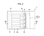
- Fig. 2 is a plan view of the recording head according to the embodiment.
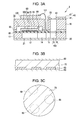
- Fig. 3A is a sectional view of the recording head according to the embodiment
- Fig. 3B is an enlarged sectional view of a major portion of the recording head shown in Fig. 3A
- Fig. 3C is an enlarged plan view of the major portion.
- Figs. 4A and 4B are sectional views showing a manufacturing process of the recording head according to the embodiment.
- Figs. 5A to 5C are sectional views showing the manufacturing process of the recording head according to the embodiment.
- Figs. 6A to 6C are sectional views showing the manufacturing process of the recording head according to the embodiment.
- Figs. 7A to 7C are sectional views showing the manufacturing process of the recording head according to the embodiment.
- Figs. 8A and 8B are sectional views showing the manufacturing process of the recording head according to the embodiment.
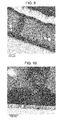
- Fig. 9 is an EFTEM-BF image of a piezoelectric element of Example 1.
- Fig. 10 is an enlarged EFTEM-BF image of the piezoelectric element of Example 1.
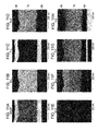
- Figs. 11A to 11H are STEM-EDS map images of the piezoelectric element of Example 1.
- Fig. 12 is a plot of the X-ray diffraction patterns of Examples 1 to 4 and Comparative Examples 1 and 2.
- Fig. 13 is a metallurgical micrograph of the surface of the piezoelectric layer of Example 1.
- Fig. 14 is a metallurgical micrograph of the surface of the piezoelectric layer of Comparative Example 1.
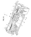
- Fig. 15 is a schematic view of a recording apparatus according to an embodiment of the invention.
- Fig. 1 is an exploded perspective view of an ink jet recording head, which is a type of liquid ejecting head, according to an embodiment of the invention.
- Fig. 2 is a plan view of the ink jet recording head shown in Fig. 1 .
- Fig. 3A is the sectional view taken along line IIIA-IIIA in Fig. 2
- Fig. 3B is an enlarged sectional view of a major portion of the structure shown in Fig. 3A
- Fig. 3C is an enlarged plan view of the major portion viewed from the second electrode side.
- a flow channel substrate 10 is made of a (110) plane-oriented monocrystalline silicon, and a silicon dioxide elastic film 50 having a thickness of 0.5 to 2 ⁇ m is disposed on one surface of the flow channel substrate 10.
- the elastic film 50 forms a vibration plate.
- the flow channel substrate 10 has pressure generating chambers 12 that have been formed by anisotropic etching performed from the side of the other surface of the flow channel substrate 10.
- the pressure generating chambers 12 are separated by a plurality of partition members 11 and are arranged in parallel in the direction of the alignment of the nozzle apertures 21 from which the same color ink is ejected. This direction is hereinafter referred to as the pressure generating chamber parallel arrangement direction or the first direction, and the direction perpendicular to the first direction is referred to as the second direction.
- ink supply channels 14 and communication paths 15 each separated by the partition members 11 are formed.
- a communicating section 13 is formed at one end of the communication paths 15.
- the communicating section 13 defines part of a manifold 100 that acts as a common ink chamber (liquid chamber) of the pressure generating chambers 12.
- the flow channel substrate 10 has liquid flow channels including the pressure generating chambers 12, the ink supply channels 14, the communication paths 15 and the communicating section 13.
- Each ink supply channel 14 communicates with one end in the second direction of the corresponding pressure generating chamber 12 and has a smaller section than the pressure generating chamber 12.
- the widths of the flow channels between the manifold 100 and the pressure generating chambers 12 are reduced on the pressure generating chamber 12 side so that the ink supply channels 14 have a smaller width than the pressure generating chambers 12.
- the ink supply channels 14 are thus formed by narrowing the flow channels from one side in the present embodiment, the flow channels may be narrowed from both sides in another embodiment.
- the ink supply channels 14 may be formed by reducing the depth of the flow channels, instead of narrowing the flow channels.
- Each communication path 15 communicates with the end of the ink supply channel 14 opposite to the pressure generating chamber 12, and has a larger cross section (in the width (first) direction) than the ink supply channel 14.
- the communication path 15 has the same cross section as the pressure generating chamber 12.
- the flow channel substrate 10 is joined to a nozzle plate 20 at the open side thereof with an adhesive, a thermal fusion film or the like.
- the nozzle plate 20 has nozzle apertures 21 communicating with portions around the ends of the corresponding pressure generating chambers 12 opposite to the ink supply channels 14.
- the nozzle plate 20 can be made of, for example, glass-ceramic, monocrystalline silicon or stainless steel.
- the above-mentioned elastic film 50 is disposed, and an adhesion layer 56 having a thickness of, for example, about 30 to 50 nm and made of titanium oxide or the like is disposed on the elastic film 50 to enhance the adhesion between the elastic film 50 and the overlying first electrode 60, as shown in Fig. 3A .
- the elastic film 50 may be provided thereon with an insulating film made of zirconium oxide or the like, if necessary.
- piezoelectric elements 300 are disposed on the adhesion layer 56.
- Each piezoelectric element 300 has a multilayer structure including a first electrode 60 made of platinum, a piezoelectric layer 70 having a small thickness of 3 ⁇ m or less, preferably 0.3 to 1.5 ⁇ m, on the upper side of the first electrode 60, and a second electrode 80 on the upper side of the piezoelectric layer 70.
- the phrase "on the upper side" of something mentioned herein means that it may be directly disposed on something or disposed with another member therebetween.
- the piezoelectric element 300 mentioned herein refers to the portion including the first electrode 60, the piezoelectric layer 70 and the second electrode 80.
- one of the electrodes of the piezoelectric element 300 acts as a common electrode, and the other electrode and the piezoelectric layer 70 are formed for each pressure generating chamber 12 by patterning.
- the first electrode 60 acts as the common electrode of the piezoelectric elements 300 and individual second electrodes 80 are provided as discrete electrodes of the piezoelectric elements 300, the functions of the first and second electrodes may be reversed for the sake of convenience of arrangement of the driving circuit and wiring.
- the piezoelectric element 300 disposed in a displaceable manner refers to an actuator device.
- the elastic film 50, the adhesion layer 56 and the first electrode 60 constitute the vibration plate
- the vibration plate is not limited to this structure.
- only the first electrode 60 may act as the vibration plate without using the elastic film 50 or the adhesion layer 56.
- the piezoelectric element 300 may double as a vibration plate.
- the piezoelectric material of the piezoelectric layer 70 is a complex oxide having a perovskite structure containing bismuth (Bi), such as a bismuth ferrate-based complex oxide or a bismuth titanate-based complex oxide.
- Exemplary bismuth ferrate-based complex oxides include bismuth ferrate (BiFeO 3 ), bismuth ferrate aluminate (Bi(Fe, Al)O 3 ), bismuth ferrate manganate (Bi(Fe, Mn)O 3 ), bismuth lanthanum ferrate manganate ((Bi, La)(Fe, Mn)O 3 ), bismuth barium ferrate manganate titanate ((Bi, Ba)(Fe, Mn, Ti)O 3 ), bismuth ferrate cobaltate (Bi(Fe, Co)O 3 ), bismuth cerium ferrate (Bi, Ce)FeO 3 ), bismuth cerium ferrate manganate ((Bi,
- Exemplary bismuth titanate-based complex oxides include bismuth sodium potassium titanate ((Bi, Na, K)TiO 3 ), bismuth barium sodium titanate zincate ((Bi, Na, Ba)(Zn, Ti)O 3 ), and bismuth barium sodium titanate cuprate ((Bi, Na, Ba)(Cu, Ti)O 3 ). Also, bismuth potassium titanate ((Bi, K)TiO 3 ), bismuth chromate (BiCrO 3 ) and other ceramics may be used.
- Bi(Zn 1/2 Ti 1/2 )O 3 , (Bi 1/2 K 1/2 )TiO 3 , (Bi 1/2 Na 1/2 )TiO 3 , (Li, Na, K)(Ta, Nb)O 3 , or the like may be added to those complex oxides.
- the piezoelectric layer 70 is made of a complex oxide having a perovskite structure expressed as bismuth barium ferrate manganate titanate ((Bi, Ba)(Fe, Mn, Ti)O 3 ), or a mixed crystal of bismuth ferrate manganate and barium titanate.
- This complex oxide is a single crystal (mixed crystal) of uniformly mixed solid solutions of bismuth ferrate manganate and barium titanate.
- the A site of the perovskite structure expressed by ABO 3 has 12 oxygen ligands, and the B site has 6 oxygen ligands to form an octahedron. Bi and Ba are present in the A site, and Fe, Mn and Ti are present in the B site.
- the complex oxide having a perovskite structure containing bismuth, barium, iron, manganese and titanium has a composition expressed by the following general formula (1).
- general formula (1) represents a composition according to the stoichiometry, unavoidable deviation from the stoichiometric composition, resulting from elemental diffusion, lattice mismatch, deficient oxygen or the like is acceptable.
- an oxide containing bismuth and platinum is present at the interface of the piezoelectric layer 70 with the first electrode 60, as shown in Fig. 3B .
- oxide portions 65 made of an oxide containing bismuth and platinum are disposed between the piezoelectric layer 70 and the first electrode 60.
- the oxide containing bismuth and platinum is hereinafter referred to as oxide portion(s) 65.
- the oxide portions 65 are made of an oxide containing bismuth and platinum, such as bismuth platinate having a pyrochlore structure.
- Bismuth platinate may be Bi 2 Pt 2 O 7 , and the valences of its elements may be varied to form a different chemical formula from Bi 2 Pt 2 O 7 .
- the oxide containing bismuth and platinum may have a pyrochlore structure, and part of bismuth or platinum may be substituted with other elements.
- the oxide portions 65 at the interface of the piezoelectric layer 70 made of a complex oxide having a bismuth-based perovskite structure with the first electrode 60 made of platinum By forming the oxide portions 65 at the interface of the piezoelectric layer 70 made of a complex oxide having a bismuth-based perovskite structure with the first electrode 60 made of platinum, the occurrence of cracks in the piezoelectric layer 70 can be reduced. Although the piezoelectric layer 70 made of a bismuth-based piezoelectric material is liable to crack during the production and after a certain time has elapsed from the production, the occurrence of such cracks can be reduced by providing the oxide portion 65. Details will be described later.
- the oxide portion 65 made of an oxide containing bismuth and platinum is electrically conductive and can function as an electrode. Accordingly, the oxide portion 65 does not reduce the voltage applied to the piezoelectric layer 70, and the same voltage as in the case of the structure not having the oxide portion 65 can be applied to the piezoelectric layer 70.
- the piezoelectric material of the piezoelectric layer 70 and the oxide containing bismuth and platinum of the oxide portion 65 are both oxides and contain bismuth, the piezoelectric layer 70 and the oxide portion 65 can adhere tightly with each other.
- the platinum first electrode 60 and the oxide portion 65 made of an oxide containing bismuth and platinum both contain platinum, the first electrode 60 and the oxide portion 65 can adhere tightly with each other.
- the oxide portion 65 is not limited how the oxide portion 65 is provided, and it may be formed over the entire interface of the piezoelectric layer 70 with the first electrode 60.
- the oxide portion 65 is formed in an island manner, as shown in Fig. 3B .
- An island manner refers to a state where the oxide portion 65 is provided so as not to cover the entire interface between the piezoelectric layer 70 and the first electrode 60, and, preferably, a plurality of oxide portions 65 are disposed at intervals.
- the shape of the oxide portion 65 is not particularly limited, and may be circular or oval as shown in Fig. 3C when viewed from the second electrode 80 side.
- the second electrode 80 provided for each piezoelectric element 300 is connected with a lead electrode 90 made of, for example, gold (Au) extending from the end of the second electrode 80 on the ink supply channel 14 side to the upper surface of the elastic film 50 and, optionally, to the upper surface of an insulating film.
- a lead electrode 90 made of, for example, gold (Au) extending from the end of the second electrode 80 on the ink supply channel 14 side to the upper surface of the elastic film 50 and, optionally, to the upper surface of an insulating film.
- a protective substrate 30 having a manifold section 31 defining at least part of a manifold 100 is joined to the flow channel substrate 10 having the piezoelectric elements 300 with an adhesive 35 so as to cover the first electrode 60, the elastic film 50, an optionally provided insulating film, and the lead electrodes 90.
- the manifold section 31 passes through the thickness of the protective substrate 30 and extends along the widths of the pressure generating chambers 12.
- the manifold section 31 communicates with the communicating section 13 of the flow channel substrate 10 to form the manifold 100 acting as the common ink chamber of the pressure generating chambers 12.
- the communicating section 13 of the flow channel substrate 10 may be divided for each pressure generating chamber 12, and only the manifold section 31 may serve as the manifold.
- the flow channel substrate 10 may have only the pressure generating chambers 12, and the manifold 100 and ink supply channels 14 communicating with the respective pressure generating chambers 12 are formed in a member between the flow channel substrate 10 and the protective substrate 30, such as the elastic film 50 and an optionally provided insulating film.
- a piezoelectric element-protecting section 32 is disposed in the region of the protective substrate 30 opposing the piezoelectric elements 300.
- the piezoelectric element-protecting section 32 has a space so that the piezoelectric elements 300 can operate without interference. It is intended that the space of the piezoelectric element-protecting section 32 is such a size that the piezoelectric elements 300 can operate, and may or may not be sealed.
- the protective substrate 30 is made of a material having substantially the same thermal expansion coefficient as the flow channel substrate 10, such as glass or ceramic.
- the protective substrate 30 is made of the same monocrystalline silicon as the flow channel substrate 10.
- the protective substrate 30 has a through hole 33 passing through the thickness of the protective substrate 30.
- the ends of the lead electrodes 90 extending from the piezoelectric elements 300 are exposed in the through hole 33.
- a driving circuit 120 is secured on the protective substrate 30 and drives the piezoelectric elements 300 arranged in parallel.
- the driving circuit 120 may be a circuit board, a semiconductor integrated circuit (IC) or the like.
- the driving circuit 120 is electrically connected to each lead electrode 90 with a conductive connection wire 121, such as bonding wire.
- a compliance substrate 40 including a sealing film 41 and a fixing plate 42 is joined on the protective substrate 30.
- the sealing film 41 is made of a flexible material having a low rigidity, and seals one end of the manifold section 31.
- the fixing plate 42 is made of a relatively hard material. The portion of the fixing plate 42 opposing the manifold 100 is completely removed to form an opening 43; hence the manifold 100 is closed at one end only with the flexible sealing film 41.
- the ink jet recording head I of the present embodiment draws an ink through an ink inlet connected to an external ink supply unit (not shown).
- the ink is delivered to fill the spaces from the manifold 100 to the nozzle apertures 21.
- the ink jet recording head I applies a voltage between the first electrode 60 and each second electrode 80 corresponding to the pressure generating chambers 12, according to the recording signal from the driving circuit 120.
- the elastic film 50, the first electrode 60 and the piezoelectric layers 70 are deformed to increase the internal pressure in the pressure generating chambers 12, thereby ejecting the ink through the nozzle apertures 21.
- FIGS. 4A to 8B are sectional views of the pressure generating chamber taken in the longitudinal direction.
- a silicon dioxide (SiO 2 ) film is formed for an elastic film 50 on the surface of a flow channel substrate silicon wafer 110 by thermal oxidation or the like.
- an adhesion layer 56 is formed of, for example, titanium oxide on the SiO 2 elastic film 50 by sputtering, thermal oxidation or the like, as shown in Fig. 4B .
- a first electrode 60 is formed over the entire surface of the adhesion layer 56, as shown in Fig. 5A . More specifically, a platinum first electrode 60 is formed on the adhesion layer 56 by sputtering or vapor deposition. Then, the first electrode 60 and the adhesion layer 56 are simultaneously patterned so that their sides are inclined, through a resist mask (not shown) having a predetermined shape on the first electrode, as shown in Fig. 5B .
- the piezoelectric layer 70 may be formed by any method without particular limitation.
- a chemical solution method may be applied, such as a sol-gel method or a metal-organic decomposition (MOD) method in which a solution of metal complexes each containing Bi, Fe, Mn, Ti or Ba dissolved or dispersed in a solvent is applied onto the first electrode 60, and the coating of the solution is dried and then fired to form a metal oxide piezoelectric layer (piezoelectric film).
- the piezoelectric layer 70 can be formed by other methods, such as sputtering, pulsed laser deposition (PLD), CVD or aerosol deposition, irrespective of liquid process or solid process.
- the method for forming the oxide portion 65 is not particularly limited as well, and the oxide portion 65 may be formed by, for example, sputtering or PLD.
- Both the oxide portion 65 and the piezoelectric layer 70 may be formed by a series of operations using a chemical solution method, such as MOD or a sol-gel method. More specifically, the oxide portion 65 and the piezoelectric layer 70 are formed by a series of operations as below.
- a sol or MOD solution (precursor solution) containing metal complexes each containing Bi, Fe, Mn, Ti or Ba in a desired proportion is applied onto the first electrode 60 by spin coating or the like to form a piezoelectric precursor film 71 (coating).
- the precursor solution to be applied is prepared by dissolving or dispersing in an organic solution a mixture of metal complexes that can produce a complex oxide containing Bi, Fe, Mn, Ba and Ti.
- the mixture of metal complexes contains metal complexes each containing at least one of the metals constituting the complex oxide, and the metal complexes are mixed so that Fe, Mn, Ti and Ba have desired mole ratios while the mole ratio of Bi is 10 mol% or more higher than the mole ratio of the desired composition.
- the metal complexes each containing Bi, Fe, Mn, Ba or Ti are mixed in such a proportion as metals Fe, Mn, Ti and Ba can form a complex oxide expressed as a mixed crystal of desired bismuth ferrate manganate and barium titanate while the mole ratio of Bi is higher by 10 mol% or more, more preferably by 10 mol% to 30 mol%, than that of the Bi of the complex oxide.
- Metal complexes containing Bi, Fe, Mn, Ba or Ta include metal alkoxides, organic acid salts, and ⁇ -diketone complexes.
- the metal complex containing Bi may be bismuth 2-ethylhexanoate or bismuth acetate.
- the metal complex containing Fe may be iron 2-ethylhexanoate or iron acetate.
- the metal complex containing Mn may be manganese 2-ethylhexanoate or manganese acetate.
- Examples of the metal complex containing Ba include barium isopropoxide, barium 2-ethylhexanoate, and barium acetylacetonate.
- metal complex containing Ti examples include titanium isopropoxide, titanium 2-ethylhexanoate, and titanium diisopropoxide bis(acetylacetonate).
- Metal complexes containing two or more metals of Bi, Fe, Mn, Ba and Ti may be used.
- the solvent can be selected from various types of solvents that can dissolve or disperse the mixture of the metal complexes, such as toluene, xylene, octane, ethylene glycol, 2-methoxyphenol, butanol, ethanol, isopropyl alcohol, acetic acid, and water, without particular limitation. These solvents may be used in combination.
- the piezoelectric precursor film 71 is dried for a certain time by being heated to a predetermined temperature (for example, 130 to 200°C) (drying). Then, the dried piezoelectric precursor film 71 is degreased by being heated to a predetermined temperature (for example, 350 to 450°C) and allowed to stand at that temperature for a certain time (degreasing).
- the degreasing mentioned herein is performed to convert organic components in the piezoelectric precursor film 71 into, for example, NO 2 , CO 2 or H 2 O and thus to remove the organic components.
- the drying and degreasing may be performed in any atmosphere without particular limitation, and may be performed in air, an oxygen atmosphere or an inert gas atmosphere. The operations for coating, drying and degreasing may be repeated.
- the piezoelectric precursor film 71 is crystallized by being heated to a predetermined temperature, such as a temperature of about 600 to 850°C, and allowed to stand at that temperature for a certain time, such as for 1 to 10 minutes.
- a piezoelectric film 72 is formed which is made of a piezoelectric material containing a complex oxide expressed as a mixed crystal of bismuth ferrate manganate and barium titanate (firing).
- the firing operation may be performed in any atmosphere without particular limitation, and may be performed in air, an oxygen atmosphere or an inert gas atmosphere.
- the heating apparatus used for the drying, degreasing and firing operations may be a rapid thermal annealing (RTA) apparatus using an infrared lamp for heating, or a hot plate.
- RTA rapid thermal annealing
- the piezoelectric layer 70 has a predetermined thickness, including the piezoelectric films 72, as shown in Fig. 6B , with oxide portions 65 at the interface of the piezoelectric layer 70 with the first electrode 60, as shown in Fig. 6C , which is a fragmentary enlarged view of the major portion of Fig. 6B .
- the operations of coating, drying, degreasing and firing may be performed step by step, or the firing operation may be performed at one time after the sequence of operations of coating, drying and degreasing has been repeated.
- the piezoelectric layer 70 may include only a single piezoelectric film 72 in another embodiment.
- a layer for second electrodes 80 is formed of platinum on the piezoelectric layer 70 by sputtering or the like, and the piezoelectric layer 70 and the layer for the second electrodes 80 are simultaneously patterned so as to form piezoelectric elements 300, each including the first electrode 60, the piezoelectric layer 70 and the second electrode 80, in regions corresponding to the pressure generating chambers 12, as shown in Fig. 7A .
- the patterning of the piezoelectric layer 70 and the second electrode 80 can be performed at one time by dry etching through a resist layer (not shown) having a predetermined shape. After this operation, post-annealing may be performed at a temperature in the range of 600 to 800°C, if necessary.
- favorable interfaces can be formed between the piezoelectric layer 70 and the first electrode 60 and between the piezoelectric layer 70 and the second electrode 80, and, in addition, the crystallinity of the piezoelectric layer 70 can be enhanced.
- a film is formed of, for example, gold (Au), over the entire surface of the flow channel substrate wafer 110, and is patterned into lead electrodes 90 for each piezoelectric element 300, as shown in Fig. 7B , through a mask pattern (not shown) made of, for example, resist.
- Au gold
- a silicon protective substrate wafer 130 for a plurality of protective substrates 30 is bonded to the piezoelectric element 300 side of the flow channel substrate wafer 110 with an adhesive 35, and the thickness of the flow channel substrate wafer 110 is reduced to a predetermined level, as shown in Fig. 7C .
- a mask layer is formed on the surface of the flow channel substrate wafer 110 opposite to the protective substrate wafer 130 and is patterned into a mask 52 having a predetermined shape.
- the flow channel substrate wafer 110 is subjected to anisotropic etching (wet etching) using an alkaline solution, such as KOH, through the mask 52 to form the pressure generating chambers 12 corresponding to the piezoelectric elements 300, the communicating section 13, the ink supply channels 14 and the communication paths 15 therein.
- anisotropic etching wet etching
- alkaline solution such as KOH
- a silicon dioxide film was formed to a thickness of 1200 nm on a (110)-oriented monocrystalline silicon substrate by thermal oxidation.
- a titanium film was formed to a thickness of 40 nm on the silicon dioxide film by RF magnetron sputtering, and was then oxidized to form a titanium oxide film.
- a platinum film was formed to a thickness of 100 nm on the titanium oxide film by RF magnetron sputtering, thus forming a (111)-oriented first electrode 60.
- a precursor solution was prepared by mixing bismuth 2-ethylhexanoate, iron acetylacetonate, barium acetate, titanium isopropoxide and manganese acetylacetonate in n-butanol so that each metal was in the proportion shown in Table 1.
- the precursor solution was dropped onto the surface of the substrate on which the titanium oxide film and the first electrode 60 had been formed, and was then subjected to spin coating at a speed of 3000 rpm, thus forming a piezoelectric precursor film (coating). Then, the piezoelectric precursor film on the substrate was dried on a hot plate at 180°C for 2 minutes (drying). The piezoelectric precursor film was further subjected to degreasing on a hot plate at 450°C for 2 minutes (degreasing). The sequence of the operations of coating, drying and degreasing was performed twice, and, then, the resulting precursor films were fired at 750°C for 5 minutes in an oxygen atmosphere using a rapid thermal annealing (RTA) apparatus (firing).
- RTA rapid thermal annealing
- a sequence of performing the sequence of the operations of coating, drying and degreasing four times and, subsequently, the operation of firing all the precursor films was performed twice.
- a piezoelectric layer 70 was formed to a thickness of 660 nm by 10 coating operations in total.
- a platinum film having a diameter of 500 ⁇ m and a thickness of 100 nm was formed as second electrodes 80 on the piezoelectric layer 70 by DC sputtering, and was then fired at 750°C for 5 minutes by RTA to complete a piezoelectric element.
- oxide portions 65 having thicknesses of about 60 nm were formed between the piezoelectric layer 70 and the first electrode 60, as shown in Figs. 9 and 10 (see portions indicated by arrows).
- the oxide portions 65 were formed in an island manner on the first electrode 60.
- the oxide portions 65 were formed at the interface of the piezoelectric layer 70 with the first electrode 60, but were not formed in the middle in the thickness direction or on the second electrode 80 side of the piezoelectric layer 70.
- the scanning electron microscopy high-angle annular dark field (STEM-HAADF) and the Bi, Pt, Fe, Mn, Ba, Ti and O of the piezoelectric element of Example 1 were observed at a section along the thickness direction of the piezoelectric element by scanning transmission electron microscope-energy-dispersive spectroscopy (STEM-EDS).
- STEM-EDS scanning transmission electron microscope-energy-dispersive spectroscopy
- the oxide portion 65 contained Pt, Bi and O.
- the piezoelectric layer 70 contained Bi, Fe, Mn, Ba, Ti and O.
- the piezoelectric elements of Examples 1 to 4 and Comparative Examples 1 and 2 were subjected to powder X-ray diffraction analysis to obtain the diffraction pattern of the piezoelectric layer with D8 Discover (manufactured by Bruker AXS) using CuK ⁇ rays at room temperature. The results are shown in Fig. 12 .
- a peak representing a perovskite structure and a peak representing the substrate were observed. More specifically, a peak representing (100) orientation of the piezoelectric layer made of a single phase of a perovskite structure was observed around 23°, a peak representing (110) orientation of the silicon substrate was observed around 32°, and a peak representing (111) orientation of Pt was observed around 40°.
- the invention is not limited to the disclosed embodiment.
- a monocrystalline silicon substrate is used as the flow channel substrate 10.
- the flow channel substrate 10 may be made of, for example, silicon-on-insulator (SOI) or glass, without particular limitation.
- the piezoelectric element 300 of the above embodiment includes the first electrode 60, the piezoelectric layer 70 and the second electrode 80 that are stacked in that order on a substrate (flow channel substrate 10), the structure of the piezoelectric element is not limited to this structure.
- an embodiment of the invention can be applied to a vertical vibration piezoelectric element including layers of a piezoelectric material and an electrode material alternately formed so as to expand and contract in the axis direction.
- the ink jet recording head according to an embodiment of the invention can be installed in an ink jet recording apparatus to serve as a part of a recording head unit including flow channels communicating with an ink cartridge or the like.
- Fig. 15 is a schematic perspective view of such an ink jet recording apparatus.
- the ink jet recording apparatus II shown in Fig. 15 includes recording head units 1A and 1 B each including the ink jet recording head I, and cartridges 2A and 2B for supplying ink are removably mounted in the respective recoding head units 1A and 1 B.
- the recording head units 1A and 1 B are loaded on a carriage 3 secured for movement along a carriage shaft 5 of an apparatus body 4.
- the recording head units 1A and 1 B eject, for example, a black ink composition and a color ink composition, respectively.
- the carriage 3 on which the recording head units 1A and 1 B are mounted is moved along the carriage shaft 5 by transmitting a driving force from a driving motor 6 to the carriage 3 through a plurality of gears (not shown) and a timing belt 7.
- a platen 8 is disposed along the carriage shaft 5 so that a recording sheet S, which is a print medium such as a paper sheet, fed from, for example, a feed roller (not shown), is transported over the platen 8.
- liquid ejecting head As the liquid ejecting head, the invention is intended for any type of liquid ejecting head, and may be applied to other liquid ejecting heads that eject liquid other than ink.
- Other liquid ejecting heads include various types of recording head used in image recording apparatuses such as printers, color material ejecting heads used for manufacturing color filters of liquid crystal displays or the like, electrode material ejecting heads used for forming electrodes of organic EL displays or field emission displays (FEDs), and bioorganic material ejecting heads used for manufacturing bio-chips.
- the piezoelectric element of embodiments of the invention can be used in ultrasonic oscillators and other ultrasonic wave devices, ultrasonic motors, IR sensors, ultrasonic sensors, thermal sensors, pressure sensors, pyroelectric sensors, acceleration sensors, gyroscopic sensors, and other sensors, without being limited to the piezoelectric element used in liquid ejecting heads represented by an ink jet recording head.
- the invention can be applied to ferroelectric memory devices and other ferroelectric elements, liquid micropumps, thin-film ceramic capacitors, gate insulating films and so forth.
Landscapes
- Engineering & Computer Science (AREA)
- Manufacturing & Machinery (AREA)
- Chemical & Material Sciences (AREA)
- Ceramic Engineering (AREA)
- Particle Formation And Scattering Control In Inkjet Printers (AREA)
Abstract
Description
- The present invention relates to a liquid ejecting head and a liquid ejecting apparatus, each including a pressure generating chamber communicating with a nozzle aperture and a piezoelectric element that includes a piezoelectric layer and electrodes applying a voltage to the piezoelectric layer and functions to change the pressure in the pressure generating chamber, and relates to the piezoelectric element.
- Some piezoelectric elements used in liquid ejecting heads have a structure in which a piezoelectric layer made of a piezoelectric material capable of electromechanical conversion, such as a crystallized dielectric material, is disposed between two electrodes. This type of piezoelectric element can be used as a deflection vibration mode actuator device in a liquid ejecting head. Ink jet recording heads are a typical type of liquid ejecting head. An ink jet recording head includes a vibration plate defining a part of a pressure generating chamber communicating with nozzle apertures through which ink droplets are ejected. In the ink jet recording head, a piezoelectric element deforms the vibration plate to apply a pressure to the ink in the pressure generating chamber, thereby ejecting ink droplets through the nozzle apertures.
- The piezoelectric ceramic film of the piezoelectric element is required to have high piezoelectric properties, and a typical example of the piezoelectric material is lead zirconate titanate (PZT) (see
JP-A-2001-223404 JP-A-2009-252789 - However, bismuth ferrate-based piezoelectric materials are liable to crack during production and after a certain time has elapsed from production.
- This issue arises not only in ink jet recording heads, but also in other liquid ejecting heads that eject droplets other than ink, and piezoelectric elements used for applications other than liquid ejecting heads have the same issue.
- An advantage of some aspects of the invention is that it provides a liquid ejecting head and a liquid ejecting apparatus that have low environmental load and in which the occurrence of cracks is suppressed, and provides a piezoelectric element used in the liquid ejecting head and the liquid ejecting apparatus.
- According to an aspect of the invention, a liquid ejecting head is provided which includes a pressure generating chamber communicating with a nozzle aperture, and a piezoelectric element. The piezoelectric element includes a first electrode made of platinum, a piezoelectric layer on the first electrode, made of a complex oxide having a perovskite structure containing at least bismuth, and a second electrode on the piezoelectric layer. In addition, an oxide containing bismuth and platinum is disposed at the interface of the piezoelectric layer with the first electrode.
- In this embodiment, the portion of the oxide containing bismuth and platinum contributes to reducing the occurrence of cracks in the piezoelectric layer made of a bismuth based-piezoelectric material. In addition, since the lead content can be reduced, the environmental load can be reduced.
- Preferably, the piezoelectric layer may further contain iron. More preferably, the piezoelectric layer may further contain manganese and titanium.
- Preferably, the oxide containing bismuth and platinum is made of bismuth platinate having a pyrochlore structure. Thus, cracks in the piezoelectric layer made of a bismuth-based piezoelectric material can be reliably suppressed.
- Preferably, the oxide containing bismuth and platinum is disposed in an island manner. Thus, the adhesion between the oxide and the piezoelectric layer is enhanced.
- According to another aspect of the invention, a liquid ejection apparatus including the above-described liquid ejection head is provided. Since the liquid ejecting apparatus includes the piezoelectric element whose environmental load is reduced and in which the occurrence of cracks is suppressed, the liquid ejecting apparatus can be reliable.
- According to another aspect of the invention, a piezoelectric element is provided which includes a first electrode made of platinum, a piezoelectric layer on the first electrode, made of a complex oxide having a perovskite structure containing at least bismuth, and a second electrode on the piezoelectric layer. In addition, an oxide containing bismuth and platinum is disposed at the interface of the piezoelectric layer with the first electrode.
- In the piezoelectric element of this embodiment, cracks in the piezoelectric layer made of a bismuth-based piezoelectric material are suppressed. In addition, since the lead content can be reduced, the environmental load can be reduced.
- Embodiments of the invention will now be described by way of example only with reference to the accompanying drawings, wherein like numbers reference like elements.
-
Fig. 1 is a schematic exploded perspective view of a recording head according to an embodiment of the invention. -
Fig. 2 is a plan view of the recording head according to the embodiment. -
Fig. 3A is a sectional view of the recording head according to the embodiment,Fig. 3B is an enlarged sectional view of a major portion of the recording head shown inFig. 3A, and Fig. 3C is an enlarged plan view of the major portion. -
Figs. 4A and 4B are sectional views showing a manufacturing process of the recording head according to the embodiment. -
Figs. 5A to 5C are sectional views showing the manufacturing process of the recording head according to the embodiment. -
Figs. 6A to 6C are sectional views showing the manufacturing process of the recording head according to the embodiment. -
Figs. 7A to 7C are sectional views showing the manufacturing process of the recording head according to the embodiment. -
Figs. 8A and 8B are sectional views showing the manufacturing process of the recording head according to the embodiment. -
Fig. 9 is an EFTEM-BF image of a piezoelectric element of Example 1. -
Fig. 10 is an enlarged EFTEM-BF image of the piezoelectric element of Example 1. -
Figs. 11A to 11H are STEM-EDS map images of the piezoelectric element of Example 1. -
Fig. 12 is a plot of the X-ray diffraction patterns of Examples 1 to 4 and Comparative Examples 1 and 2. -
Fig. 13 is a metallurgical micrograph of the surface of the piezoelectric layer of Example 1. -
Fig. 14 is a metallurgical micrograph of the surface of the piezoelectric layer of Comparative Example 1. -
Fig. 15 is a schematic view of a recording apparatus according to an embodiment of the invention. -
Fig. 1 is an exploded perspective view of an ink jet recording head, which is a type of liquid ejecting head, according to an embodiment of the invention.Fig. 2 is a plan view of the ink jet recording head shown inFig. 1 .Fig. 3A is the sectional view taken along line IIIA-IIIA inFig. 2 ,Fig. 3B is an enlarged sectional view of a major portion of the structure shown inFig. 3A, and Fig. 3C is an enlarged plan view of the major portion viewed from the second electrode side. - As shown in these figures, a
flow channel substrate 10 is made of a (110) plane-oriented monocrystalline silicon, and a silicon dioxideelastic film 50 having a thickness of 0.5 to 2 µm is disposed on one surface of theflow channel substrate 10. Theelastic film 50 forms a vibration plate. - The
flow channel substrate 10 haspressure generating chambers 12 that have been formed by anisotropic etching performed from the side of the other surface of theflow channel substrate 10. Thepressure generating chambers 12 are separated by a plurality ofpartition members 11 and are arranged in parallel in the direction of the alignment of thenozzle apertures 21 from which the same color ink is ejected. This direction is hereinafter referred to as the pressure generating chamber parallel arrangement direction or the first direction, and the direction perpendicular to the first direction is referred to as the second direction. At one end of thepressure generating chambers 12 in the second direction,ink supply channels 14 andcommunication paths 15 each separated by thepartition members 11 are formed. A communicatingsection 13 is formed at one end of thecommunication paths 15. The communicatingsection 13 defines part of a manifold 100 that acts as a common ink chamber (liquid chamber) of thepressure generating chambers 12. Thus, theflow channel substrate 10 has liquid flow channels including thepressure generating chambers 12, theink supply channels 14, thecommunication paths 15 and the communicatingsection 13. - Each
ink supply channel 14 communicates with one end in the second direction of the correspondingpressure generating chamber 12 and has a smaller section than thepressure generating chamber 12. For example, in the present embodiment, the widths of the flow channels between the manifold 100 and thepressure generating chambers 12 are reduced on thepressure generating chamber 12 side so that theink supply channels 14 have a smaller width than thepressure generating chambers 12. Although theink supply channels 14 are thus formed by narrowing the flow channels from one side in the present embodiment, the flow channels may be narrowed from both sides in another embodiment. Alternatively, theink supply channels 14 may be formed by reducing the depth of the flow channels, instead of narrowing the flow channels. Eachcommunication path 15 communicates with the end of theink supply channel 14 opposite to thepressure generating chamber 12, and has a larger cross section (in the width (first) direction) than theink supply channel 14. In the present embodiment, thecommunication path 15 has the same cross section as thepressure generating chamber 12. - The
flow channel substrate 10 is joined to anozzle plate 20 at the open side thereof with an adhesive, a thermal fusion film or the like. Thenozzle plate 20 hasnozzle apertures 21 communicating with portions around the ends of the correspondingpressure generating chambers 12 opposite to theink supply channels 14. Thenozzle plate 20 can be made of, for example, glass-ceramic, monocrystalline silicon or stainless steel. - On the opposite side to the open side of the
flow channel substrate 10, the above-mentionedelastic film 50 is disposed, and anadhesion layer 56 having a thickness of, for example, about 30 to 50 nm and made of titanium oxide or the like is disposed on theelastic film 50 to enhance the adhesion between theelastic film 50 and the overlyingfirst electrode 60, as shown inFig. 3A . Theelastic film 50 may be provided thereon with an insulating film made of zirconium oxide or the like, if necessary. - Furthermore,
piezoelectric elements 300 are disposed on theadhesion layer 56. Eachpiezoelectric element 300 has a multilayer structure including afirst electrode 60 made of platinum, apiezoelectric layer 70 having a small thickness of 3 µm or less, preferably 0.3 to 1.5 µm, on the upper side of thefirst electrode 60, and asecond electrode 80 on the upper side of thepiezoelectric layer 70. The phrase "on the upper side" of something mentioned herein means that it may be directly disposed on something or disposed with another member therebetween. Thepiezoelectric element 300 mentioned herein refers to the portion including thefirst electrode 60, thepiezoelectric layer 70 and thesecond electrode 80. In general, one of the electrodes of thepiezoelectric element 300 acts as a common electrode, and the other electrode and thepiezoelectric layer 70 are formed for eachpressure generating chamber 12 by patterning. Although in the present embodiment, thefirst electrode 60 acts as the common electrode of thepiezoelectric elements 300 and individualsecond electrodes 80 are provided as discrete electrodes of thepiezoelectric elements 300, the functions of the first and second electrodes may be reversed for the sake of convenience of arrangement of the driving circuit and wiring. In the present embodiment, thepiezoelectric element 300 disposed in a displaceable manner refers to an actuator device. Although in the structure shown inFig. 1 , theelastic film 50, theadhesion layer 56 and thefirst electrode 60 constitute the vibration plate, the vibration plate is not limited to this structure. For example, only thefirst electrode 60 may act as the vibration plate without using theelastic film 50 or theadhesion layer 56. Thepiezoelectric element 300 may double as a vibration plate. - The piezoelectric material of the
piezoelectric layer 70 is a complex oxide having a perovskite structure containing bismuth (Bi), such as a bismuth ferrate-based complex oxide or a bismuth titanate-based complex oxide. Exemplary bismuth ferrate-based complex oxides include bismuth ferrate (BiFeO3), bismuth ferrate aluminate (Bi(Fe, Al)O3), bismuth ferrate manganate (Bi(Fe, Mn)O3), bismuth lanthanum ferrate manganate ((Bi, La)(Fe, Mn)O3), bismuth barium ferrate manganate titanate ((Bi, Ba)(Fe, Mn, Ti)O3), bismuth ferrate cobaltate (Bi(Fe, Co)O3), bismuth cerium ferrate (Bi, Ce)FeO3), bismuth cerium ferrate manganate ((Bi, Ce)(Fe, Mn)O3), bismuth lanthanum cerium ferrate ((Bi, La, Ce)FeO3), bismuth lanthanum cerium ferrate manganate ((Bi, La, Ce)(Fe, Mn)O3), bismuth samarium ferrate ((Bi, Sm)FeO3), bismuth barium ferrate manganate titanate ((Bi, Ba)(Fe, Mn, Ti)O3), bismuth ferrate chromate (Bi(Cr, Fe)O3), bismuth potassium ferrate manganate titanate ((Bi, K)(Fe, Mn, Ti)O3), and bismuth barium ferrate manganate zincate titanate ((Bi, Ba)(Fe, Mn, Zn, Ti)O3). Exemplary bismuth titanate-based complex oxides include bismuth sodium potassium titanate ((Bi, Na, K)TiO3), bismuth barium sodium titanate zincate ((Bi, Na, Ba)(Zn, Ti)O3), and bismuth barium sodium titanate cuprate ((Bi, Na, Ba)(Cu, Ti)O3). Also, bismuth potassium titanate ((Bi, K)TiO3), bismuth chromate (BiCrO3) and other ceramics may be used. Bi(Zn1/2Ti1/2)O3, (Bi1/2K1/2)TiO3, (Bi1/2Na1/2)TiO3, (Li, Na, K)(Ta, Nb)O3, or the like may be added to those complex oxides. - In the present embodiment, the
piezoelectric layer 70 is made of a complex oxide having a perovskite structure expressed as bismuth barium ferrate manganate titanate ((Bi, Ba)(Fe, Mn, Ti)O3), or a mixed crystal of bismuth ferrate manganate and barium titanate. This complex oxide is a single crystal (mixed crystal) of uniformly mixed solid solutions of bismuth ferrate manganate and barium titanate. The A site of the perovskite structure expressed by ABO3 has 12 oxygen ligands, and the B site has 6 oxygen ligands to form an octahedron. Bi and Ba are present in the A site, and Fe, Mn and Ti are present in the B site. - Preferably, the complex oxide having a perovskite structure containing bismuth, barium, iron, manganese and titanium has a composition expressed by the following general formula (1). However, since general formula (1) represents a composition according to the stoichiometry, unavoidable deviation from the stoichiometric composition, resulting from elemental diffusion, lattice mismatch, deficient oxygen or the like is acceptable.
(1-x){Bi(FE1-a, Mna)O3}-x{BaTiO3} (1)
where 0.1≤x≤0.4 and 0.01≤a≤0.1 - In the present embodiment, an oxide containing bismuth and platinum is present at the interface of the
piezoelectric layer 70 with thefirst electrode 60, as shown inFig. 3B . In other words,oxide portions 65 made of an oxide containing bismuth and platinum are disposed between thepiezoelectric layer 70 and thefirst electrode 60. The oxide containing bismuth and platinum is hereinafter referred to as oxide portion(s) 65. - The
oxide portions 65 are made of an oxide containing bismuth and platinum, such as bismuth platinate having a pyrochlore structure. Bismuth platinate may be Bi2Pt2O7, and the valences of its elements may be varied to form a different chemical formula from Bi2Pt2O7. The oxide containing bismuth and platinum may have a pyrochlore structure, and part of bismuth or platinum may be substituted with other elements. - By forming the
oxide portions 65 at the interface of thepiezoelectric layer 70 made of a complex oxide having a bismuth-based perovskite structure with thefirst electrode 60 made of platinum, the occurrence of cracks in thepiezoelectric layer 70 can be reduced. Although thepiezoelectric layer 70 made of a bismuth-based piezoelectric material is liable to crack during the production and after a certain time has elapsed from the production, the occurrence of such cracks can be reduced by providing theoxide portion 65. Details will be described later. - The
oxide portion 65 made of an oxide containing bismuth and platinum is electrically conductive and can function as an electrode. Accordingly, theoxide portion 65 does not reduce the voltage applied to thepiezoelectric layer 70, and the same voltage as in the case of the structure not having theoxide portion 65 can be applied to thepiezoelectric layer 70. - Also, since the piezoelectric material of the
piezoelectric layer 70 and the oxide containing bismuth and platinum of theoxide portion 65 are both oxides and contain bismuth, thepiezoelectric layer 70 and theoxide portion 65 can adhere tightly with each other. In addition, since the platinumfirst electrode 60 and theoxide portion 65 made of an oxide containing bismuth and platinum both contain platinum, thefirst electrode 60 and theoxide portion 65 can adhere tightly with each other. - It is not limited how the
oxide portion 65 is provided, and it may be formed over the entire interface of thepiezoelectric layer 70 with thefirst electrode 60. Preferably, theoxide portion 65 is formed in an island manner, as shown inFig. 3B . An island manner refers to a state where theoxide portion 65 is provided so as not to cover the entire interface between thepiezoelectric layer 70 and thefirst electrode 60, and, preferably, a plurality ofoxide portions 65 are disposed at intervals. By providing theoxide portions 65 in an island manner, a rough interface is formed between theoxide portions 65 and thepiezoelectric layer 70, so that the adhesion between theoxide portions 65 and thepiezoelectric layer 70 is enhanced. The shape of theoxide portion 65 is not particularly limited, and may be circular or oval as shown inFig. 3C when viewed from thesecond electrode 80 side. - The
second electrode 80 provided for eachpiezoelectric element 300 is connected with alead electrode 90 made of, for example, gold (Au) extending from the end of thesecond electrode 80 on theink supply channel 14 side to the upper surface of theelastic film 50 and, optionally, to the upper surface of an insulating film. - A
protective substrate 30 having amanifold section 31 defining at least part of a manifold 100 is joined to theflow channel substrate 10 having thepiezoelectric elements 300 with an adhesive 35 so as to cover thefirst electrode 60, theelastic film 50, an optionally provided insulating film, and thelead electrodes 90. Themanifold section 31 passes through the thickness of theprotective substrate 30 and extends along the widths of thepressure generating chambers 12. Thus, themanifold section 31 communicates with the communicatingsection 13 of theflow channel substrate 10 to form the manifold 100 acting as the common ink chamber of thepressure generating chambers 12. The communicatingsection 13 of theflow channel substrate 10 may be divided for eachpressure generating chamber 12, and only themanifold section 31 may serve as the manifold. Alternatively, theflow channel substrate 10 may have only thepressure generating chambers 12, and the manifold 100 andink supply channels 14 communicating with the respectivepressure generating chambers 12 are formed in a member between theflow channel substrate 10 and theprotective substrate 30, such as theelastic film 50 and an optionally provided insulating film. - A piezoelectric element-protecting
section 32 is disposed in the region of theprotective substrate 30 opposing thepiezoelectric elements 300. The piezoelectric element-protectingsection 32 has a space so that thepiezoelectric elements 300 can operate without interference. It is intended that the space of the piezoelectric element-protectingsection 32 is such a size that thepiezoelectric elements 300 can operate, and may or may not be sealed. - Preferably, the
protective substrate 30 is made of a material having substantially the same thermal expansion coefficient as theflow channel substrate 10, such as glass or ceramic. In the present embodiment, theprotective substrate 30 is made of the same monocrystalline silicon as theflow channel substrate 10. - The
protective substrate 30 has a throughhole 33 passing through the thickness of theprotective substrate 30. The ends of thelead electrodes 90 extending from thepiezoelectric elements 300 are exposed in the throughhole 33. - A driving
circuit 120 is secured on theprotective substrate 30 and drives thepiezoelectric elements 300 arranged in parallel. The drivingcircuit 120 may be a circuit board, a semiconductor integrated circuit (IC) or the like. The drivingcircuit 120 is electrically connected to eachlead electrode 90 with aconductive connection wire 121, such as bonding wire. - Furthermore, a
compliance substrate 40 including a sealingfilm 41 and a fixingplate 42 is joined on theprotective substrate 30. The sealingfilm 41 is made of a flexible material having a low rigidity, and seals one end of themanifold section 31. The fixingplate 42 is made of a relatively hard material. The portion of the fixingplate 42 opposing the manifold 100 is completely removed to form anopening 43; hence the manifold 100 is closed at one end only with theflexible sealing film 41. - The ink jet recording head I of the present embodiment draws an ink through an ink inlet connected to an external ink supply unit (not shown). The ink is delivered to fill the spaces from the manifold 100 to the
nozzle apertures 21. Then, the ink jet recording head I applies a voltage between thefirst electrode 60 and eachsecond electrode 80 corresponding to thepressure generating chambers 12, according to the recording signal from the drivingcircuit 120. Thus, theelastic film 50, thefirst electrode 60 and thepiezoelectric layers 70 are deformed to increase the internal pressure in thepressure generating chambers 12, thereby ejecting the ink through thenozzle apertures 21. - A method for manufacturing the ink jet recording head according to the present embodiment will be described with reference to
Figs. 4A to 8B. Figs. 4A to 8B are sectional views of the pressure generating chamber taken in the longitudinal direction. - As shown in
Fig. 4A , a silicon dioxide (SiO2) film is formed for anelastic film 50 on the surface of a flow channelsubstrate silicon wafer 110 by thermal oxidation or the like. Then, anadhesion layer 56 is formed of, for example, titanium oxide on the SiO2elastic film 50 by sputtering, thermal oxidation or the like, as shown inFig. 4B . - Subsequently, a
first electrode 60 is formed over the entire surface of theadhesion layer 56, as shown inFig. 5A . More specifically, a platinumfirst electrode 60 is formed on theadhesion layer 56 by sputtering or vapor deposition. Then, thefirst electrode 60 and theadhesion layer 56 are simultaneously patterned so that their sides are inclined, through a resist mask (not shown) having a predetermined shape on the first electrode, as shown inFig. 5B . - Then, after removing the resist mask, an
oxide portion 65 andpiezoelectric layers 70 are formed on the first electrode 60 (and the adhesion layer 56). Thepiezoelectric layer 70 may be formed by any method without particular limitation. For example, a chemical solution method may be applied, such as a sol-gel method or a metal-organic decomposition (MOD) method in which a solution of metal complexes each containing Bi, Fe, Mn, Ti or Ba dissolved or dispersed in a solvent is applied onto thefirst electrode 60, and the coating of the solution is dried and then fired to form a metal oxide piezoelectric layer (piezoelectric film). Thepiezoelectric layer 70 can be formed by other methods, such as sputtering, pulsed laser deposition (PLD), CVD or aerosol deposition, irrespective of liquid process or solid process. - The method for forming the
oxide portion 65 is not particularly limited as well, and theoxide portion 65 may be formed by, for example, sputtering or PLD. - Both the
oxide portion 65 and thepiezoelectric layer 70 may be formed by a series of operations using a chemical solution method, such as MOD or a sol-gel method. More specifically, theoxide portion 65 and thepiezoelectric layer 70 are formed by a series of operations as below. First, as shown inFig. 5C , a sol or MOD solution (precursor solution) containing metal complexes each containing Bi, Fe, Mn, Ti or Ba in a desired proportion is applied onto thefirst electrode 60 by spin coating or the like to form a piezoelectric precursor film 71 (coating). - The precursor solution to be applied is prepared by dissolving or dispersing in an organic solution a mixture of metal complexes that can produce a complex oxide containing Bi, Fe, Mn, Ba and Ti. The mixture of metal complexes contains metal complexes each containing at least one of the metals constituting the complex oxide, and the metal complexes are mixed so that Fe, Mn, Ti and Ba have desired mole ratios while the mole ratio of Bi is 10 mol% or more higher than the mole ratio of the desired composition. More specifically, the metal complexes each containing Bi, Fe, Mn, Ba or Ti are mixed in such a proportion as metals Fe, Mn, Ti and Ba can form a complex oxide expressed as a mixed crystal of desired bismuth ferrate manganate and barium titanate while the mole ratio of Bi is higher by 10 mol% or more, more preferably by 10 mol% to 30 mol%, than that of the Bi of the complex oxide.
- Metal complexes containing Bi, Fe, Mn, Ba or Ta include metal alkoxides, organic acid salts, and β-diketone complexes. The metal complex containing Bi may be bismuth 2-ethylhexanoate or bismuth acetate. The metal complex containing Fe may be iron 2-ethylhexanoate or iron acetate. The metal complex containing Mn may be manganese 2-ethylhexanoate or manganese acetate. Examples of the metal complex containing Ba include barium isopropoxide, barium 2-ethylhexanoate, and barium acetylacetonate. Examples of the metal complex containing Ti include titanium isopropoxide, titanium 2-ethylhexanoate, and titanium diisopropoxide bis(acetylacetonate). Metal complexes containing two or more metals of Bi, Fe, Mn, Ba and Ti may be used.
- The solvent can be selected from various types of solvents that can dissolve or disperse the mixture of the metal complexes, such as toluene, xylene, octane, ethylene glycol, 2-methoxyphenol, butanol, ethanol, isopropyl alcohol, acetic acid, and water, without particular limitation. These solvents may be used in combination.
- Subsequently, the
piezoelectric precursor film 71 is dried for a certain time by being heated to a predetermined temperature (for example, 130 to 200°C) (drying). Then, the driedpiezoelectric precursor film 71 is degreased by being heated to a predetermined temperature (for example, 350 to 450°C) and allowed to stand at that temperature for a certain time (degreasing). The degreasing mentioned herein is performed to convert organic components in thepiezoelectric precursor film 71 into, for example, NO2, CO2 or H2O and thus to remove the organic components. The drying and degreasing may be performed in any atmosphere without particular limitation, and may be performed in air, an oxygen atmosphere or an inert gas atmosphere. The operations for coating, drying and degreasing may be repeated. - Then, as shown in
Fig. 6A , thepiezoelectric precursor film 71 is crystallized by being heated to a predetermined temperature, such as a temperature of about 600 to 850°C, and allowed to stand at that temperature for a certain time, such as for 1 to 10 minutes. Thus apiezoelectric film 72 is formed which is made of a piezoelectric material containing a complex oxide expressed as a mixed crystal of bismuth ferrate manganate and barium titanate (firing). The firing operation may be performed in any atmosphere without particular limitation, and may be performed in air, an oxygen atmosphere or an inert gas atmosphere. - The heating apparatus used for the drying, degreasing and firing operations may be a rapid thermal annealing (RTA) apparatus using an infrared lamp for heating, or a hot plate.
- The operations of coating, drying and degreasing, or the operations of coating, drying, degreasing and firing are repeated according to the desired thickness, thus forming a plurality of
piezoelectric films 72. Thus, thepiezoelectric layer 70 has a predetermined thickness, including thepiezoelectric films 72, as shown inFig. 6B , withoxide portions 65 at the interface of thepiezoelectric layer 70 with thefirst electrode 60, as shown inFig. 6C , which is a fragmentary enlarged view of the major portion ofFig. 6B . For forming thepiezoelectric films 72, the operations of coating, drying, degreasing and firing may be performed step by step, or the firing operation may be performed at one time after the sequence of operations of coating, drying and degreasing has been repeated. Althoughpiezoelectric films 72 are formed on top of one another in the present embodiment, thepiezoelectric layer 70 may include only a singlepiezoelectric film 72 in another embodiment. - After the
piezoelectric layer 70 is formed, a layer forsecond electrodes 80 is formed of platinum on thepiezoelectric layer 70 by sputtering or the like, and thepiezoelectric layer 70 and the layer for thesecond electrodes 80 are simultaneously patterned so as to formpiezoelectric elements 300, each including thefirst electrode 60, thepiezoelectric layer 70 and thesecond electrode 80, in regions corresponding to thepressure generating chambers 12, as shown inFig. 7A . The patterning of thepiezoelectric layer 70 and thesecond electrode 80 can be performed at one time by dry etching through a resist layer (not shown) having a predetermined shape. After this operation, post-annealing may be performed at a temperature in the range of 600 to 800°C, if necessary. Thus, favorable interfaces can be formed between thepiezoelectric layer 70 and thefirst electrode 60 and between thepiezoelectric layer 70 and thesecond electrode 80, and, in addition, the crystallinity of thepiezoelectric layer 70 can be enhanced. - Then, a film is formed of, for example, gold (Au), over the entire surface of the flow
channel substrate wafer 110, and is patterned intolead electrodes 90 for eachpiezoelectric element 300, as shown inFig. 7B , through a mask pattern (not shown) made of, for example, resist. - Then, a silicon protective substrate wafer 130 for a plurality of
protective substrates 30 is bonded to thepiezoelectric element 300 side of the flowchannel substrate wafer 110 with an adhesive 35, and the thickness of the flowchannel substrate wafer 110 is reduced to a predetermined level, as shown inFig. 7C . - Turning to
Fig. 8A , a mask layer is formed on the surface of the flowchannel substrate wafer 110 opposite to the protective substrate wafer 130 and is patterned into amask 52 having a predetermined shape. - Subsequently, as shown in
Fig. 8B , the flowchannel substrate wafer 110 is subjected to anisotropic etching (wet etching) using an alkaline solution, such as KOH, through themask 52 to form thepressure generating chambers 12 corresponding to thepiezoelectric elements 300, the communicatingsection 13, theink supply channels 14 and thecommunication paths 15 therein. - Then, unnecessary outer portions of the flow
channel substrate wafer 110 and protective substrate wafer 130 are cut off by, for example, dicing. Subsequently, anozzle plate 20 havingnozzle apertures 21 therein is joined to the surface of the flowchannel substrate wafer 110 opposite the protective substrate wafer 130 after themask 52 has been removed, and acompliance substrate 40 is joined to the protective substrate wafer 130. The flowchannel substrate wafer 110 joined to other substrates is cut into chips as shown inFig. 1 , each including aflow channel substrate 10 and other members. Thus, the ink jet recording head I of the present embodiment is completed. - The invention will be further described in detail with reference to Examples below. However, the invention is not limited to the following Examples.
- First, a silicon dioxide film was formed to a thickness of 1200 nm on a (110)-oriented monocrystalline silicon substrate by thermal oxidation. Subsequently, a titanium film was formed to a thickness of 40 nm on the silicon dioxide film by RF magnetron sputtering, and was then oxidized to form a titanium oxide film. Then, a platinum film was formed to a thickness of 100 nm on the titanium oxide film by RF magnetron sputtering, thus forming a (111)-oriented
first electrode 60. - A precursor solution was prepared by mixing bismuth 2-ethylhexanoate, iron acetylacetonate, barium acetate, titanium isopropoxide and manganese acetylacetonate in n-butanol so that each metal was in the proportion shown in Table 1.
- The precursor solution was dropped onto the surface of the substrate on which the titanium oxide film and the
first electrode 60 had been formed, and was then subjected to spin coating at a speed of 3000 rpm, thus forming a piezoelectric precursor film (coating). Then, the piezoelectric precursor film on the substrate was dried on a hot plate at 180°C for 2 minutes (drying). The piezoelectric precursor film was further subjected to degreasing on a hot plate at 450°C for 2 minutes (degreasing). The sequence of the operations of coating, drying and degreasing was performed twice, and, then, the resulting precursor films were fired at 750°C for 5 minutes in an oxygen atmosphere using a rapid thermal annealing (RTA) apparatus (firing). - Subsequently, a sequence of performing the sequence of the operations of coating, drying and degreasing four times and, subsequently, the operation of firing all the precursor films was performed twice. Thus, a
piezoelectric layer 70 was formed to a thickness of 660 nm by 10 coating operations in total. - Then, a platinum film having a diameter of 500 µm and a thickness of 100 nm was formed as
second electrodes 80 on thepiezoelectric layer 70 by DC sputtering, and was then fired at 750°C for 5 minutes by RTA to complete a piezoelectric element.Table 1 Excess of Bi Bi Mole ratio Ba Mole ratio Fe Mole ratio Ti Mole ratio Mn Mole ratio Example 1 10 mol% 0.7500 0.2500 0.7125 0.2500 0.0375 Example 2 12 mol% 0.8100 0.2500 0.7125 0.2500 0.0375 Example 3 14 mol% 0.8250 0.2500 0.7125 0.2500 0.0375 Example 4 16 mol% 0.8400 0.2500 0.7125 0.2500 0.0375 Comparative Example 1 0 mol% 0.8550 0.2500 0.7125 0.2500 0.0375 Comparative Example 2 8 mol% 0.8700 0.2500 0.7125 0.2500 0.0375 - The section along the thickness direction of the piezoelectric element of Example 1 was observed through an EFTEM (energy-filtering transmission electron microscope). The EFTEM-BF (Bright Field) image obtained is shown in
Fig. 9 . Also,Fig. 10 shows an enlargement of a part ofFig. 9 . - As a result, it was found that
oxide portions 65 having thicknesses of about 60 nm were formed between thepiezoelectric layer 70 and thefirst electrode 60, as shown inFigs. 9 and 10 (see portions indicated by arrows). Theoxide portions 65 were formed in an island manner on thefirst electrode 60. Theoxide portions 65 were formed at the interface of thepiezoelectric layer 70 with thefirst electrode 60, but were not formed in the middle in the thickness direction or on thesecond electrode 80 side of thepiezoelectric layer 70. - The scanning electron microscopy high-angle annular dark field (STEM-HAADF) and the Bi, Pt, Fe, Mn, Ba, Ti and O of the piezoelectric element of Example 1 were observed at a section along the thickness direction of the piezoelectric element by scanning transmission electron microscope-energy-dispersive spectroscopy (STEM-EDS). For the Bi, Pt and Ba, their L shells were observed. For the Fe, Mn, Ti and O, their K shells were observed. The results are shown in
Figs. 11A to 11H . As shown in these figures, theoxide portion 65 contained Pt, Bi and O. Thepiezoelectric layer 70 contained Bi, Fe, Mn, Ba, Ti and O. - The piezoelectric elements of Examples 1 to 4 and Comparative Examples 1 and 2 were subjected to powder X-ray diffraction analysis to obtain the diffraction pattern of the piezoelectric layer with D8 Discover (manufactured by Bruker AXS) using CuKα rays at room temperature. The results are shown in
Fig. 12 . - In all of Examples 1 to 4 and Comparative Examples 1 and 2, a peak representing a perovskite structure and a peak representing the substrate were observed. More specifically, a peak representing (100) orientation of the piezoelectric layer made of a single phase of a perovskite structure was observed around 23°, a peak representing (110) orientation of the silicon substrate was observed around 32°, and a peak representing (111) orientation of Pt was observed around 40°.
- In addition, in Examples 1 to 4, a peak derived from a pyrochlore structure was observed around 30°. On the other hand, in Comparative Examples 1 and 2, the peak derived from a pyrochlore structure was not observed.
- The results of
Examinations 1 to 3 show thatoxide portions 65 made of bismuth platinate having a pyrochlore structure were formed at the interface of thepiezoelectric layer 70 with thefirst electrode 60 in Examples 1 to 4, in which the mole ratio of Bi was adjusted so as to be 10 mol% or more higher than the mole ratio of a desired composition. - It was observed for 7 days after the formation of the
piezoelectric layer 70 whether or not thepiezoelectric layer 70, not having thesecond electrode 80, was cracked, for Examples 1 to 4 and Comparative Examples 1 and 2. It was determined that samples not cracked were good, and that samples cracked were bad. The results are shown in Table 2. The surface of thepiezoelectric layer 70 after one day had elapsed from its formation was observed at a magnification of 1000 times through a metallurgical micrograph in a dark field mode, for Example 1 and Comparative Example 1. The result of Example 1 is shown inFig. 13 , and the result of Comparative Example 1 is shown inFig. 14 . - In Examples 1 to 4 in which
oxide portions 65 made of bismuth platinate having a pyrochlore structure were formed at the interface of thepiezoelectric layer 70 with thefirst electrode 60, cracks were not observed. On the other hand, in Comparative Examples 1 and 2 in whichoxide portions 65 made of bismuth platinate having a pyrochlore structure were not formed at the interface of thepiezoelectric layer 70 with thefirst electrode 60, cracks were observed after 24 hours had elapsed.Table 2 Excess of Bi After one hour After 24 hours After 7 days Example 1 10 mol% Good Good Good Example 2 12 mol% Good Good Good Example 3 14 mol% Good Good Good Example 4 16 mol% Good Good Good Comparative Example 1 0 mol% Good Bad Bad Comparative Example 2 8 mol% Good Bad Bad - Although an exemplary embodiment of the invention has been described, the invention is not limited to the disclosed embodiment. For example, in the above embodiment, a monocrystalline silicon substrate is used as the
flow channel substrate 10. However, theflow channel substrate 10 may be made of, for example, silicon-on-insulator (SOI) or glass, without particular limitation. - Also, although the
piezoelectric element 300 of the above embodiment includes thefirst electrode 60, thepiezoelectric layer 70 and thesecond electrode 80 that are stacked in that order on a substrate (flow channel substrate 10), the structure of the piezoelectric element is not limited to this structure. For example, an embodiment of the invention can be applied to a vertical vibration piezoelectric element including layers of a piezoelectric material and an electrode material alternately formed so as to expand and contract in the axis direction. - The ink jet recording head according to an embodiment of the invention can be installed in an ink jet recording apparatus to serve as a part of a recording head unit including flow channels communicating with an ink cartridge or the like.
Fig. 15 is a schematic perspective view of such an ink jet recording apparatus. - The ink jet recording apparatus II shown in
Fig. 15 includesrecording head units cartridges recoding head units recording head units carriage 3 secured for movement along acarriage shaft 5 of anapparatus body 4. Therecording head units - The
carriage 3 on which therecording head units carriage shaft 5 by transmitting a driving force from a drivingmotor 6 to thecarriage 3 through a plurality of gears (not shown) and atiming belt 7. In theapparatus body 4, aplaten 8 is disposed along thecarriage shaft 5 so that a recording sheet S, which is a print medium such as a paper sheet, fed from, for example, a feed roller (not shown), is transported over theplaten 8. - Although the above embodiment has described an ink jet recording head as the liquid ejecting head, the invention is intended for any type of liquid ejecting head, and may be applied to other liquid ejecting heads that eject liquid other than ink. Other liquid ejecting heads include various types of recording head used in image recording apparatuses such as printers, color material ejecting heads used for manufacturing color filters of liquid crystal displays or the like, electrode material ejecting heads used for forming electrodes of organic EL displays or field emission displays (FEDs), and bioorganic material ejecting heads used for manufacturing bio-chips.
- The piezoelectric element of embodiments of the invention can be used in ultrasonic oscillators and other ultrasonic wave devices, ultrasonic motors, IR sensors, ultrasonic sensors, thermal sensors, pressure sensors, pyroelectric sensors, acceleration sensors, gyroscopic sensors, and other sensors, without being limited to the piezoelectric element used in liquid ejecting heads represented by an ink jet recording head. Furthermore, the invention can be applied to ferroelectric memory devices and other ferroelectric elements, liquid micropumps, thin-film ceramic capacitors, gate insulating films and so forth.
- The foregoing description has been given by way of example only and it will be appreciated by a person skilled in the art that modifications can be made without departing from the scope of the present invention.
Claims (7)
- A piezoelectric element (300) comprising:a first electrode (60) made of platinum;a piezoelectric layer (70) disposed on the first electrode, made of a complex oxide having a perovskite structure containing at least bismuth; anda second electrode (80) disposed on the piezoelectric layer,wherein an oxide (65) containing bismuth and platinum is disposed at the interface of the piezoelectric layer with the first electrode.
- A piezoelectric element according to Claim 1, wherein the piezoelectric layer further contains iron.
- A piezoelectric element according to Claim 2, wherein the piezoelectric layer further contains manganese and titanium.
- A piezoelectric element according to any one of the preceding claims, wherein the oxide containing bismuth and platinum is bismuth palatinate having a pyrochlore structure.
- A piezoelectric element according to any one of the preceding claims, wherein the oxide containing bismuth and platinum is disposed in an island manner.
- A liquid ejecting head (I) comprising:a pressure generating chamber (12) communicating with a nozzle aperture (21); anda piezoelectric element (300) according to any one of the preceding claims.
- A liquid ejecting apparatus comprising the liquid ejecting head as set forth in Claim 6.
Applications Claiming Priority (1)
| Application Number | Priority Date | Filing Date | Title |
|---|---|---|---|
| JP2011096599A JP5790922B2 (en) | 2011-04-22 | 2011-04-22 | Piezoelectric element, liquid ejecting head, liquid ejecting apparatus, ultrasonic device and sensor |
Publications (3)
| Publication Number | Publication Date |
|---|---|
| EP2515357A2 true EP2515357A2 (en) | 2012-10-24 |
| EP2515357A3 EP2515357A3 (en) | 2014-04-16 |
| EP2515357B1 EP2515357B1 (en) | 2017-01-11 |
Family
ID=46087445
Family Applications (1)
| Application Number | Title | Priority Date | Filing Date |
|---|---|---|---|
| EP12164994.1A Not-in-force EP2515357B1 (en) | 2011-04-22 | 2012-04-20 | Liquid ejecting head, liquid ejecting apparatus, and piezoelectric element |
Country Status (3)
| Country | Link |
|---|---|
| US (1) | US8746856B2 (en) |
| EP (1) | EP2515357B1 (en) |
| JP (1) | JP5790922B2 (en) |
Cited By (2)
| Publication number | Priority date | Publication date | Assignee | Title |
|---|---|---|---|---|
| JP2014192268A (en) * | 2013-03-26 | 2014-10-06 | Seiko Epson Corp | Liquid injection head, liquid injection apparatus, and piezoelectric element |
| EP3581682A4 (en) * | 2017-02-07 | 2020-11-25 | Kabushiki Kaisha Toyota Chuo Kenkyusho | ELECTROLYSIS ANODE |
Citations (2)
| Publication number | Priority date | Publication date | Assignee | Title |
|---|---|---|---|---|
| JP2001223404A (en) | 2000-02-08 | 2001-08-17 | Seiko Epson Corp | Piezoelectric element, ink jet recording head, method of manufacturing these, and ink jet printer |
| JP2009252789A (en) | 2008-04-01 | 2009-10-29 | Seiko Epson Corp | Piezoelectric material and piezoelectric element |
Family Cites Families (10)
| Publication number | Priority date | Publication date | Assignee | Title |
|---|---|---|---|---|
| JPH11145412A (en) * | 1997-11-14 | 1999-05-28 | Sony Corp | Electronic device and its manufacturing method, dielectric capacitor and its manufacturing method, and ferroelectric nonvolatile memory device and its manufacturing method |
| JP4015820B2 (en) * | 2001-04-11 | 2007-11-28 | 日本碍子株式会社 | Wiring board and manufacturing method thereof |
| JP4842523B2 (en) * | 2004-07-02 | 2011-12-21 | 日本碍子株式会社 | Wiring board |
| US8212451B2 (en) | 2006-10-31 | 2012-07-03 | Kyocera Corporation | Multi-layer piezoelectric element having a plurality of junction sections and injection apparatus employing the same |
| JP4775772B2 (en) | 2008-04-01 | 2011-09-21 | セイコーエプソン株式会社 | Piezoelectric material and piezoelectric element |
| JP5329863B2 (en) * | 2008-07-31 | 2013-10-30 | 富士フイルム株式会社 | Piezoelectric element, method for manufacturing piezoelectric element, and liquid ejection device |
| JP5410780B2 (en) * | 2009-02-18 | 2014-02-05 | 富士フイルム株式会社 | Film formation method, film formation apparatus, piezoelectric film, piezoelectric element, and liquid ejection apparatus |
| US8400047B2 (en) * | 2009-03-12 | 2013-03-19 | Canon Kabushiki Kaisha | Piezoelectric material, piezoelectric device, and method of producing the piezoelectric device |
| US8405285B2 (en) | 2009-06-08 | 2013-03-26 | Fujifilm Corporation | Piezoelectric device, piezoelectric actuator having the same, liquid discharge apparatus, and power generating apparatus |
| EP2443269A2 (en) * | 2009-06-19 | 2012-04-25 | Ceramatec, Inc | Bismuth metal oxide pyrochlores as electrode materials |
-
2011
- 2011-04-22 JP JP2011096599A patent/JP5790922B2/en not_active Expired - Fee Related
-
2012
- 2012-04-19 US US13/451,095 patent/US8746856B2/en not_active Expired - Fee Related
- 2012-04-20 EP EP12164994.1A patent/EP2515357B1/en not_active Not-in-force
Patent Citations (2)
| Publication number | Priority date | Publication date | Assignee | Title |
|---|---|---|---|---|
| JP2001223404A (en) | 2000-02-08 | 2001-08-17 | Seiko Epson Corp | Piezoelectric element, ink jet recording head, method of manufacturing these, and ink jet printer |
| JP2009252789A (en) | 2008-04-01 | 2009-10-29 | Seiko Epson Corp | Piezoelectric material and piezoelectric element |
Cited By (2)
| Publication number | Priority date | Publication date | Assignee | Title |
|---|---|---|---|---|
| JP2014192268A (en) * | 2013-03-26 | 2014-10-06 | Seiko Epson Corp | Liquid injection head, liquid injection apparatus, and piezoelectric element |
| EP3581682A4 (en) * | 2017-02-07 | 2020-11-25 | Kabushiki Kaisha Toyota Chuo Kenkyusho | ELECTROLYSIS ANODE |
Also Published As
| Publication number | Publication date |
|---|---|
| JP5790922B2 (en) | 2015-10-07 |
| EP2515357A3 (en) | 2014-04-16 |
| EP2515357B1 (en) | 2017-01-11 |
| JP2012228777A (en) | 2012-11-22 |
| US8746856B2 (en) | 2014-06-10 |
| US20120268533A1 (en) | 2012-10-25 |
Similar Documents
| Publication | Publication Date | Title |
|---|---|---|
| US9356223B2 (en) | Liquid ejecting head and liquid ejecting apparatus | |
| US8721914B2 (en) | Piezoelectric element, liquid ejecting head, and liquid ejecting apparatus | |
| US8820894B2 (en) | Liquid ejecting head, liquid ejecting apparatus, piezoelectric element, and method for manufacturing the same | |
| CN102529371B (en) | Liquid ejecting head, liquid ejecting apparatus, and piezoelectric element | |
| US8636343B2 (en) | Liquid ejecting head, liquid ejecting apparatus, and piezoelectric element | |
| EP2515357B1 (en) | Liquid ejecting head, liquid ejecting apparatus, and piezoelectric element | |
| JP6372644B2 (en) | Piezoelectric element, liquid jet head and sensor | |
| US8746855B2 (en) | Method for manufacturing piezoelectric element, piezoelectric element, liquid ejecting head, and liquid ejecting apparatus | |
| JP6057049B2 (en) | Piezoelectric element, liquid ejecting head, liquid ejecting apparatus, ultrasonic device and sensor | |
| JP2011238708A (en) | Liquid ejection head manufacturing method, liquid ejection device, and piezoelectric element manufacturing method | |
| JP5880821B2 (en) | Liquid ejecting head, liquid ejecting apparatus, and piezoelectric element | |
| JP2013098442A (en) | Liquid injection head, liquid injection device and piezoelectric element | |
| JP6015892B2 (en) | Piezoelectric element, liquid ejecting head, liquid ejecting apparatus, ultrasonic device and sensor | |
| US8721054B2 (en) | Liquid ejecting head, liquid ejecting apparatus, and piezoelectric element | |
| US8783837B2 (en) | Liquid jet head, liquid jet apparatus, and piezoelectric element | |
| JP2015061048A (en) | Liquid ejecting head, liquid ejecting apparatus, and piezoelectric element | |
| JP5915848B2 (en) | Piezoelectric element manufacturing method, liquid ejecting head manufacturing method, liquid ejecting apparatus manufacturing method, ultrasonic device manufacturing method, and sensor manufacturing method | |
| JP2013091228A (en) | Liquid jet head, liquid jetting apparatus, and piezoelectric element | |
| JP2013120909A (en) | Liquid injection head, liquid injection apparatus, and piezoelectric element | |
| JP2013052641A (en) | Liquid ejecting head, liquid ejection device, and piezoelectric element |
Legal Events
| Date | Code | Title | Description |
|---|---|---|---|
| PUAI | Public reference made under article 153(3) epc to a published international application that has entered the european phase |
Free format text: ORIGINAL CODE: 0009012 |
|
| AK | Designated contracting states |
Kind code of ref document: A2 Designated state(s): AL AT BE BG CH CY CZ DE DK EE ES FI FR GB GR HR HU IE IS IT LI LT LU LV MC MK MT NL NO PL PT RO RS SE SI SK SM TR |
|
| AX | Request for extension of the european patent |
Extension state: BA ME |
|
| PUAL | Search report despatched |
Free format text: ORIGINAL CODE: 0009013 |
|
| AK | Designated contracting states |
Kind code of ref document: A3 Designated state(s): AL AT BE BG CH CY CZ DE DK EE ES FI FR GB GR HR HU IE IS IT LI LT LU LV MC MK MT NL NO PL PT RO RS SE SI SK SM TR |
|
| AX | Request for extension of the european patent |
Extension state: BA ME |
|
| RIC1 | Information provided on ipc code assigned before grant |
Ipc: H01L 41/09 20060101ALN20140313BHEP Ipc: B41J 2/14 20060101AFI20140313BHEP Ipc: H01L 41/319 20130101ALI20140313BHEP Ipc: H01L 41/187 20060101ALI20140313BHEP |
|
| 17P | Request for examination filed |
Effective date: 20141016 |
|
| RBV | Designated contracting states (corrected) |
Designated state(s): AL AT BE BG CH CY CZ DE DK EE ES FI FR GB GR HR HU IE IS IT LI LT LU LV MC MK MT NL NO PL PT RO RS SE SI SK SM TR |
|
| 17Q | First examination report despatched |
Effective date: 20150319 |
|
| REG | Reference to a national code |
Ref country code: DE Ref legal event code: R079 Ref document number: 602012027626 Country of ref document: DE Free format text: PREVIOUS MAIN CLASS: H01L0041080000 Ipc: B41J0002140000 |
|
| GRAP | Despatch of communication of intention to grant a patent |
Free format text: ORIGINAL CODE: EPIDOSNIGR1 |
|
| RIC1 | Information provided on ipc code assigned before grant |
Ipc: B41J 2/14 20060101AFI20160830BHEP Ipc: H01L 41/187 20060101ALI20160830BHEP Ipc: H01L 41/09 20060101ALN20160830BHEP Ipc: H01L 41/319 20130101ALI20160830BHEP |
|
| RIC1 | Information provided on ipc code assigned before grant |
Ipc: H01L 41/319 20130101ALI20160908BHEP Ipc: H01L 41/09 20060101ALN20160908BHEP Ipc: B41J 2/14 20060101AFI20160908BHEP Ipc: H01L 41/187 20060101ALI20160908BHEP |
|
| INTG | Intention to grant announced |
Effective date: 20160927 |
|
| GRAS | Grant fee paid |
Free format text: ORIGINAL CODE: EPIDOSNIGR3 |
|
| GRAA | (expected) grant |
Free format text: ORIGINAL CODE: 0009210 |
|
| AK | Designated contracting states |
Kind code of ref document: B1 Designated state(s): AL AT BE BG CH CY CZ DE DK EE ES FI FR GB GR HR HU IE IS IT LI LT LU LV MC MK MT NL NO PL PT RO RS SE SI SK SM TR |
|
| REG | Reference to a national code |
Ref country code: GB Ref legal event code: FG4D |
|
| REG | Reference to a national code |
Ref country code: CH Ref legal event code: EP |
|
| REG | Reference to a national code |
Ref country code: AT Ref legal event code: REF Ref document number: 860892 Country of ref document: AT Kind code of ref document: T Effective date: 20170115 |
|
| REG | Reference to a national code |
Ref country code: IE Ref legal event code: FG4D |
|
| REG | Reference to a national code |
Ref country code: DE Ref legal event code: R096 Ref document number: 602012027626 Country of ref document: DE |
|
| REG | Reference to a national code |
Ref country code: LT Ref legal event code: MG4D |
|
| REG | Reference to a national code |
Ref country code: NL Ref legal event code: MP Effective date: 20170111 |
|
| REG | Reference to a national code |
Ref country code: AT Ref legal event code: MK05 Ref document number: 860892 Country of ref document: AT Kind code of ref document: T Effective date: 20170111 |
|
| PG25 | Lapsed in a contracting state [announced via postgrant information from national office to epo] |
Ref country code: NL Free format text: LAPSE BECAUSE OF FAILURE TO SUBMIT A TRANSLATION OF THE DESCRIPTION OR TO PAY THE FEE WITHIN THE PRESCRIBED TIME-LIMIT Effective date: 20170111 |
|
| PG25 | Lapsed in a contracting state [announced via postgrant information from national office to epo] |
Ref country code: GR Free format text: LAPSE BECAUSE OF FAILURE TO SUBMIT A TRANSLATION OF THE DESCRIPTION OR TO PAY THE FEE WITHIN THE PRESCRIBED TIME-LIMIT Effective date: 20170412 Ref country code: IS Free format text: LAPSE BECAUSE OF FAILURE TO SUBMIT A TRANSLATION OF THE DESCRIPTION OR TO PAY THE FEE WITHIN THE PRESCRIBED TIME-LIMIT Effective date: 20170511 Ref country code: NO Free format text: LAPSE BECAUSE OF FAILURE TO SUBMIT A TRANSLATION OF THE DESCRIPTION OR TO PAY THE FEE WITHIN THE PRESCRIBED TIME-LIMIT Effective date: 20170411 Ref country code: HR Free format text: LAPSE BECAUSE OF FAILURE TO SUBMIT A TRANSLATION OF THE DESCRIPTION OR TO PAY THE FEE WITHIN THE PRESCRIBED TIME-LIMIT Effective date: 20170111 Ref country code: FI Free format text: LAPSE BECAUSE OF FAILURE TO SUBMIT A TRANSLATION OF THE DESCRIPTION OR TO PAY THE FEE WITHIN THE PRESCRIBED TIME-LIMIT Effective date: 20170111 Ref country code: LT Free format text: LAPSE BECAUSE OF FAILURE TO SUBMIT A TRANSLATION OF THE DESCRIPTION OR TO PAY THE FEE WITHIN THE PRESCRIBED TIME-LIMIT Effective date: 20170111 |
|
| PG25 | Lapsed in a contracting state [announced via postgrant information from national office to epo] |
Ref country code: BG Free format text: LAPSE BECAUSE OF FAILURE TO SUBMIT A TRANSLATION OF THE DESCRIPTION OR TO PAY THE FEE WITHIN THE PRESCRIBED TIME-LIMIT Effective date: 20170411 Ref country code: PL Free format text: LAPSE BECAUSE OF FAILURE TO SUBMIT A TRANSLATION OF THE DESCRIPTION OR TO PAY THE FEE WITHIN THE PRESCRIBED TIME-LIMIT Effective date: 20170111 Ref country code: AT Free format text: LAPSE BECAUSE OF FAILURE TO SUBMIT A TRANSLATION OF THE DESCRIPTION OR TO PAY THE FEE WITHIN THE PRESCRIBED TIME-LIMIT Effective date: 20170111 Ref country code: ES Free format text: LAPSE BECAUSE OF FAILURE TO SUBMIT A TRANSLATION OF THE DESCRIPTION OR TO PAY THE FEE WITHIN THE PRESCRIBED TIME-LIMIT Effective date: 20170111 Ref country code: LV Free format text: LAPSE BECAUSE OF FAILURE TO SUBMIT A TRANSLATION OF THE DESCRIPTION OR TO PAY THE FEE WITHIN THE PRESCRIBED TIME-LIMIT Effective date: 20170111 Ref country code: PT Free format text: LAPSE BECAUSE OF FAILURE TO SUBMIT A TRANSLATION OF THE DESCRIPTION OR TO PAY THE FEE WITHIN THE PRESCRIBED TIME-LIMIT Effective date: 20170511 Ref country code: RS Free format text: LAPSE BECAUSE OF FAILURE TO SUBMIT A TRANSLATION OF THE DESCRIPTION OR TO PAY THE FEE WITHIN THE PRESCRIBED TIME-LIMIT Effective date: 20170111 Ref country code: SE Free format text: LAPSE BECAUSE OF FAILURE TO SUBMIT A TRANSLATION OF THE DESCRIPTION OR TO PAY THE FEE WITHIN THE PRESCRIBED TIME-LIMIT Effective date: 20170111 |
|
| REG | Reference to a national code |
Ref country code: DE Ref legal event code: R097 Ref document number: 602012027626 Country of ref document: DE |
|
| PG25 | Lapsed in a contracting state [announced via postgrant information from national office to epo] |
Ref country code: RO Free format text: LAPSE BECAUSE OF FAILURE TO SUBMIT A TRANSLATION OF THE DESCRIPTION OR TO PAY THE FEE WITHIN THE PRESCRIBED TIME-LIMIT Effective date: 20170111 Ref country code: IT Free format text: LAPSE BECAUSE OF FAILURE TO SUBMIT A TRANSLATION OF THE DESCRIPTION OR TO PAY THE FEE WITHIN THE PRESCRIBED TIME-LIMIT Effective date: 20170111 Ref country code: SK Free format text: LAPSE BECAUSE OF FAILURE TO SUBMIT A TRANSLATION OF THE DESCRIPTION OR TO PAY THE FEE WITHIN THE PRESCRIBED TIME-LIMIT Effective date: 20170111 Ref country code: EE Free format text: LAPSE BECAUSE OF FAILURE TO SUBMIT A TRANSLATION OF THE DESCRIPTION OR TO PAY THE FEE WITHIN THE PRESCRIBED TIME-LIMIT Effective date: 20170111 Ref country code: CZ Free format text: LAPSE BECAUSE OF FAILURE TO SUBMIT A TRANSLATION OF THE DESCRIPTION OR TO PAY THE FEE WITHIN THE PRESCRIBED TIME-LIMIT Effective date: 20170111 |
|
| PLBE | No opposition filed within time limit |
Free format text: ORIGINAL CODE: 0009261 |
|
| STAA | Information on the status of an ep patent application or granted ep patent |
Free format text: STATUS: NO OPPOSITION FILED WITHIN TIME LIMIT |
|
| PG25 | Lapsed in a contracting state [announced via postgrant information from national office to epo] |
Ref country code: DK Free format text: LAPSE BECAUSE OF FAILURE TO SUBMIT A TRANSLATION OF THE DESCRIPTION OR TO PAY THE FEE WITHIN THE PRESCRIBED TIME-LIMIT Effective date: 20170111 Ref country code: SM Free format text: LAPSE BECAUSE OF FAILURE TO SUBMIT A TRANSLATION OF THE DESCRIPTION OR TO PAY THE FEE WITHIN THE PRESCRIBED TIME-LIMIT Effective date: 20170111 |
|
| REG | Reference to a national code |
Ref country code: CH Ref legal event code: PL |
|
| 26N | No opposition filed |
Effective date: 20171012 |
|
| GBPC | Gb: european patent ceased through non-payment of renewal fee |
Effective date: 20170420 |
|
| REG | Reference to a national code |
Ref country code: IE Ref legal event code: MM4A |
|
| REG | Reference to a national code |
Ref country code: FR Ref legal event code: ST Effective date: 20171229 |
|
| PG25 | Lapsed in a contracting state [announced via postgrant information from national office to epo] |
Ref country code: FR Free format text: LAPSE BECAUSE OF NON-PAYMENT OF DUE FEES Effective date: 20170502 Ref country code: MC Free format text: LAPSE BECAUSE OF FAILURE TO SUBMIT A TRANSLATION OF THE DESCRIPTION OR TO PAY THE FEE WITHIN THE PRESCRIBED TIME-LIMIT Effective date: 20170111 |
|
| PG25 | Lapsed in a contracting state [announced via postgrant information from national office to epo] |
Ref country code: GB Free format text: LAPSE BECAUSE OF NON-PAYMENT OF DUE FEES Effective date: 20170420 Ref country code: LI Free format text: LAPSE BECAUSE OF NON-PAYMENT OF DUE FEES Effective date: 20170430 Ref country code: CH Free format text: LAPSE BECAUSE OF NON-PAYMENT OF DUE FEES Effective date: 20170430 Ref country code: SI Free format text: LAPSE BECAUSE OF FAILURE TO SUBMIT A TRANSLATION OF THE DESCRIPTION OR TO PAY THE FEE WITHIN THE PRESCRIBED TIME-LIMIT Effective date: 20170111 Ref country code: LU Free format text: LAPSE BECAUSE OF NON-PAYMENT OF DUE FEES Effective date: 20170420 |
|
| REG | Reference to a national code |
Ref country code: BE Ref legal event code: MM Effective date: 20170430 |
|
| PG25 | Lapsed in a contracting state [announced via postgrant information from national office to epo] |
Ref country code: IE Free format text: LAPSE BECAUSE OF NON-PAYMENT OF DUE FEES Effective date: 20170420 |
|
| PG25 | Lapsed in a contracting state [announced via postgrant information from national office to epo] |
Ref country code: BE Free format text: LAPSE BECAUSE OF NON-PAYMENT OF DUE FEES Effective date: 20170430 |
|
| PG25 | Lapsed in a contracting state [announced via postgrant information from national office to epo] |
Ref country code: MT Free format text: LAPSE BECAUSE OF NON-PAYMENT OF DUE FEES Effective date: 20170420 |
|
| PG25 | Lapsed in a contracting state [announced via postgrant information from national office to epo] |
Ref country code: HU Free format text: LAPSE BECAUSE OF FAILURE TO SUBMIT A TRANSLATION OF THE DESCRIPTION OR TO PAY THE FEE WITHIN THE PRESCRIBED TIME-LIMIT; INVALID AB INITIO Effective date: 20120420 |
|
| PG25 | Lapsed in a contracting state [announced via postgrant information from national office to epo] |
Ref country code: CY Free format text: LAPSE BECAUSE OF NON-PAYMENT OF DUE FEES Effective date: 20170111 |
|
| PG25 | Lapsed in a contracting state [announced via postgrant information from national office to epo] |
Ref country code: MK Free format text: LAPSE BECAUSE OF FAILURE TO SUBMIT A TRANSLATION OF THE DESCRIPTION OR TO PAY THE FEE WITHIN THE PRESCRIBED TIME-LIMIT Effective date: 20170111 |
|
| PG25 | Lapsed in a contracting state [announced via postgrant information from national office to epo] |
Ref country code: TR Free format text: LAPSE BECAUSE OF FAILURE TO SUBMIT A TRANSLATION OF THE DESCRIPTION OR TO PAY THE FEE WITHIN THE PRESCRIBED TIME-LIMIT Effective date: 20170111 |
|
| PG25 | Lapsed in a contracting state [announced via postgrant information from national office to epo] |
Ref country code: AL Free format text: LAPSE BECAUSE OF FAILURE TO SUBMIT A TRANSLATION OF THE DESCRIPTION OR TO PAY THE FEE WITHIN THE PRESCRIBED TIME-LIMIT Effective date: 20170111 |
|
| PGFP | Annual fee paid to national office [announced via postgrant information from national office to epo] |
Ref country code: DE Payment date: 20200408 Year of fee payment: 9 |
|
| REG | Reference to a national code |
Ref country code: DE Ref legal event code: R119 Ref document number: 602012027626 Country of ref document: DE |
|
| PG25 | Lapsed in a contracting state [announced via postgrant information from national office to epo] |
Ref country code: DE Free format text: LAPSE BECAUSE OF NON-PAYMENT OF DUE FEES Effective date: 20211103 |