EP2512084A1 - Method to provide a single OFDM symbol to an LTE dl RF interface - Google Patents
Method to provide a single OFDM symbol to an LTE dl RF interface Download PDFInfo
- Publication number
- EP2512084A1 EP2512084A1 EP12163104A EP12163104A EP2512084A1 EP 2512084 A1 EP2512084 A1 EP 2512084A1 EP 12163104 A EP12163104 A EP 12163104A EP 12163104 A EP12163104 A EP 12163104A EP 2512084 A1 EP2512084 A1 EP 2512084A1
- Authority
- EP
- European Patent Office
- Prior art keywords
- ofdm
- complex
- symbol
- processor
- generating
- Prior art date
- Legal status (The legal status is an assumption and is not a legal conclusion. Google has not performed a legal analysis and makes no representation as to the accuracy of the status listed.)
- Withdrawn
Links
- 238000000034 method Methods 0.000 title claims abstract description 93
- 238000012545 processing Methods 0.000 claims abstract description 49
- 238000013507 mapping Methods 0.000 claims description 23
- 230000005540 biological transmission Effects 0.000 claims description 12
- 125000004122 cyclic group Chemical group 0.000 claims description 9
- 238000004891 communication Methods 0.000 claims description 6
- 230000010267 cellular communication Effects 0.000 claims description 3
- 238000010586 diagram Methods 0.000 description 11
- 230000015654 memory Effects 0.000 description 11
- 230000006870 function Effects 0.000 description 4
- 230000001413 cellular effect Effects 0.000 description 3
- 230000007774 longterm Effects 0.000 description 2
- 230000003287 optical effect Effects 0.000 description 2
- 239000013598 vector Substances 0.000 description 2
- 238000003491 array Methods 0.000 description 1
- 238000013461 design Methods 0.000 description 1
- 238000005516 engineering process Methods 0.000 description 1
- 238000012804 iterative process Methods 0.000 description 1
- 238000012986 modification Methods 0.000 description 1
- 230000004048 modification Effects 0.000 description 1
- 230000002093 peripheral effect Effects 0.000 description 1
- 238000002360 preparation method Methods 0.000 description 1
- 230000003068 static effect Effects 0.000 description 1
- 239000000126 substance Substances 0.000 description 1
- 230000000007 visual effect Effects 0.000 description 1
Images


Classifications
-
- H—ELECTRICITY
- H04—ELECTRIC COMMUNICATION TECHNIQUE
- H04L—TRANSMISSION OF DIGITAL INFORMATION, e.g. TELEGRAPHIC COMMUNICATION
- H04L27/00—Modulated-carrier systems
- H04L27/26—Systems using multi-frequency codes
-
- H—ELECTRICITY
- H04—ELECTRIC COMMUNICATION TECHNIQUE
- H04L—TRANSMISSION OF DIGITAL INFORMATION, e.g. TELEGRAPHIC COMMUNICATION
- H04L27/00—Modulated-carrier systems
- H04L27/26—Systems using multi-frequency codes
- H04L27/2601—Multicarrier modulation systems
- H04L27/2626—Arrangements specific to the transmitter only
- H04L27/2627—Modulators
- H04L27/2628—Inverse Fourier transform modulators, e.g. inverse fast Fourier transform [IFFT] or inverse discrete Fourier transform [IDFT] modulators
- H04L27/263—Inverse Fourier transform modulators, e.g. inverse fast Fourier transform [IFFT] or inverse discrete Fourier transform [IDFT] modulators modification of IFFT/IDFT modulator for performance improvement
-
- H—ELECTRICITY
- H04—ELECTRIC COMMUNICATION TECHNIQUE
- H04L—TRANSMISSION OF DIGITAL INFORMATION, e.g. TELEGRAPHIC COMMUNICATION
- H04L1/00—Arrangements for detecting or preventing errors in the information received
- H04L1/004—Arrangements for detecting or preventing errors in the information received by using forward error control
- H04L1/0056—Systems characterized by the type of code used
- H04L1/0064—Concatenated codes
- H04L1/0066—Parallel concatenated codes
-
- H—ELECTRICITY
- H04—ELECTRIC COMMUNICATION TECHNIQUE
- H04L—TRANSMISSION OF DIGITAL INFORMATION, e.g. TELEGRAPHIC COMMUNICATION
- H04L27/00—Modulated-carrier systems
- H04L27/26—Systems using multi-frequency codes
- H04L27/2601—Multicarrier modulation systems
- H04L27/2626—Arrangements specific to the transmitter only
- H04L27/2627—Modulators
- H04L27/2634—Inverse fast Fourier transform [IFFT] or inverse discrete Fourier transform [IDFT] modulators in combination with other circuits for modulation
-
- H—ELECTRICITY
- H04—ELECTRIC COMMUNICATION TECHNIQUE
- H04L—TRANSMISSION OF DIGITAL INFORMATION, e.g. TELEGRAPHIC COMMUNICATION
- H04L5/00—Arrangements affording multiple use of the transmission path
- H04L5/0001—Arrangements for dividing the transmission path
- H04L5/0003—Two-dimensional division
- H04L5/0005—Time-frequency
- H04L5/0007—Time-frequency the frequencies being orthogonal, e.g. OFDM(A) or DMT
-
- H—ELECTRICITY
- H04—ELECTRIC COMMUNICATION TECHNIQUE
- H04L—TRANSMISSION OF DIGITAL INFORMATION, e.g. TELEGRAPHIC COMMUNICATION
- H04L5/00—Arrangements affording multiple use of the transmission path
- H04L5/003—Arrangements for allocating sub-channels of the transmission path
- H04L5/0044—Allocation of payload; Allocation of data channels, e.g. PDSCH or PUSCH
-
- H—ELECTRICITY
- H04—ELECTRIC COMMUNICATION TECHNIQUE
- H04L—TRANSMISSION OF DIGITAL INFORMATION, e.g. TELEGRAPHIC COMMUNICATION
- H04L25/00—Baseband systems
- H04L25/02—Details ; arrangements for supplying electrical power along data transmission lines
- H04L25/03—Shaping networks in transmitter or receiver, e.g. adaptive shaping networks
- H04L25/03828—Arrangements for spectral shaping; Arrangements for providing signals with specified spectral properties
- H04L25/03866—Arrangements for spectral shaping; Arrangements for providing signals with specified spectral properties using scrambling
-
- H—ELECTRICITY
- H04—ELECTRIC COMMUNICATION TECHNIQUE
- H04L—TRANSMISSION OF DIGITAL INFORMATION, e.g. TELEGRAPHIC COMMUNICATION
- H04L25/00—Baseband systems
- H04L25/02—Details ; arrangements for supplying electrical power along data transmission lines
- H04L25/03—Shaping networks in transmitter or receiver, e.g. adaptive shaping networks
- H04L25/03891—Spatial equalizers
Definitions
- the present invention relates to wireless communication generally and, more particularly, to a method and/or apparatus for reducing latency on LTE DL implementation.
- LTE Long Term Evolution
- a flow diagram 10 is shown illustrating a main function 10 of a downlink (DL) layer 1 (L1) processing scheme.
- the function 10 provides input to a radio frequency (RF) interface.
- the function 10 performs a cyclic redundancy check (CRC) process 12, a turbo coding process 14, a sub-block interleaving and rate matching process 16, a scrambling process 18, a modulation process 20, a layer mapping and precoding process 22, a resource block (RB) mapping process 24, and an inverse fast Fourier transform (IFFT) calculation process 26.
- the resource block mapping process 24 produces a resource grid 28.
- the resource grid 28 contains orthogonal frequency division multiplexed (OFDM) symbols 30.
- One OFDM symbol 30 is one column in the resource grid 28.
- the resource grid 28 contains a total of 14 columns in the case of a normal cyclic prefix (CP).
- CP normal cyclic prefix
- the resource block mapping process 24 is to be completed before the inverse fast Fourier transform (IFFT) calculation process 26 is started.
- IFFT inverse fast Fourier transform
- the resource block mapping process 24 shall be completed for all UEs until the resource grid 28 is full. Only when the resource grid 28 is full can the IFFT calculation process 26 be performed on the OFDM symbols 30.
- the latency for the downlink data processing is measured from the generation of the CRC bit by the CRC process 12 until the first OFDM symbol 30 is ready for presentation to the RF interface (i.e., the inverse fast Fourier transform (IFFT) calculation process 26 has been performed on the first OFDM symbo1).
- IFFT inverse fast Fourier transform
- the present invention concerns an apparatus including a processor and a radio frequency (RF) interface.
- the processor may be configured to process downlink information such that a latency of the apparatus is determined by an amount of time involved in processing the downlink information to obtain a single orthogonal frequency division multiplexed (OFDM) symbol for presentation to the RF interface.
- OFDM orthogonal frequency division multiplexed
- the objects, features and advantages of the present invention include providing a method for implementation of an LTE DL with reduced latency that may (i) be implemented similarly for single and multi-user systems, (ii) minimize an amount of time taken to prepare a first OFDM symbol for presentation to an RF interface, and/or (iii) allow implementation of an LTE downlink with reduced processing power and power consumption.
- the system 100 may implement a wireless communications system.
- the system 100 may implement a third generation cellular communication system compliant with the 3GPP Long Term Evolution (LTE) standard.
- the system 100 generally comprises at least one base station 102 and a number of mobile units 104.
- the base station 102 may transmit signals to the mobile units 104 via a downlink channel 106.
- Each of the mobile units 104 may transmit signals to the base stations 102 via an uplink channel 108.
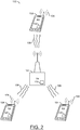
- the system 100 may also be implemented with multiple base stations 102.
- the base station(s) 102 may include a processing unit 110.
- Each of the mobile units 104 may include a processing unit 120.
- the processing units 110 and 120 may be configured to manage communications between the base station(s) 102 and the mobile units 104.
- the processing unit 110 may be configured to perform an iterative downlink process for resource elements mapping on a pipe of orthogonal frequency division multiplexed (OFDM) symbols.
- the processor 110 may implement hardware to perform the downlink processing in accordance with the present invention.
- the downlink processing in accordance with the present invention may be performed by software executed on the processing unit 110.
- the software for performing the downlink processing in accordance with the present invention may be written to a Flash memory or other nonvolatile memory (e.g., programmable read only memory (PROM), erasable programmable read only memory (EPROM), electrically erasable programmable read only memory (EEPROM), bubble memory, disk or disc media, etc.).
- volatile memory such as dynamic random access memory (DRAM) or static random access memory (SRAM) may be used.
- the software may be loaded from a non-volatile storage medium at power-up.
- the base station 102 may generate the downlink signal 106 that may be used, in one example, by mobile units 104.
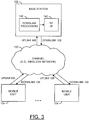
- a channel 130 may be implemented, for example, as a wireless channel.
- the channel 130 may be implemented as a cellular communications channel (e.g., a 3GPP LTE network, etc.).
- the base station 102 may include a downlink processing component 140 and a radio interface component 142.
- the downlink processing component 140 may include the processor 110 of FIG. 2 .
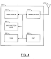
- the processing unit 200 may include, but is not limited to, a block (or module) 202, a block (or module) 204, a block (or module) 206, a block (or module) 208, a block (or module) 210, and a block (or module) 212.
- the block 202 may be implemented, in one example, as an embedded processor (e.g., ARM, etc.).
- the block 204 may be implemented as a read only memory (ROM).
- the block 206 may comprise random access memory (RAM).
- the block 208 may implement a digital signal processor (DSP).
- DSP digital signal processor
- the block 210 may be implemented, in one example, as an analog/RF unit (e.g., a transceiver). In another example, the block 210 may implement a transmitter and a receiver that are separate.
- the block 212 may implement an antenna (e.g., a cellular antenna, etc.). The block 210 may be configured to transmit and receive information via the antenna 212.
- the blocks 202-210 may be connected together using one or more busses.
- the block 204 may store computer executable instructions for controlling the processor 202 and/or the processor 208 in accordance with the teachings presented herein.
- the process 300 may implement an iterative downlink process for resource elements mapping on a pipe of orthogonal frequency division multiplexed (OFDM) symbols.
- the process (or method) 300 may comprise a step (or state) 302, a step (or state) 304, a step (or state) 306, a step (or state) 308, a step (or state) 310, a step (or state) 312, a step (or state) 314, and a step (or state) 316.
- the step 302 may comprise a cyclic redundancy check (CRC) generating process.
- the step 304 may comprise a turbo coding process.
- the step 306 may comprises a sub-block interleaving and rate matching process.
- the step 308 may comprise a scrambling process.
- the step 310 may comprise a modulation process.
- the step 312 may comprise a layer mapping and precoding process .
- the step 314 may comprise a resource block (RB) mapping process.
- the step 316 may comprise an inverse fast Fourier transform (IFFT) calculation process.
- IFFT inverse fast Fourier transform
- the cyclic redundancy check (CRC) generating process 302 generally produces several CRC parity bits.
- the resource block mapping process 314 generally produces a single orthogonal frequency division multiplexed (OFDM) symbol 318.
- a number of OFDM symbols 318 may be combined to form a resource grid similar to the resource grid 28 of FIG. 1 .
- one OFDM symbol 318 may form a column in the resource grid.
- the resource grid may comprise a total of 14 columns in the case of a normal cyclic prefix (CP). However, other numbers of columns may be implemented accordingly (e.g., in the case of an extended CP) to meet the design criteria of a particular implementation.
- the process 300 implemented in accordance with an example embodiment of the present invention does not wait until the resource grid is completely formed before performing the IFFT calculation process 316 for each OFDM symbol 318.
- the process 300 generally begins in the step 302 , In the step 302, the process 300 may generate several parity bits for an input sequence using, for example, a pre-determined cyclic generator polynomial.
- the process 300 may move to the step 304 to perform turbo coding on the data block to be transmitted to the mobile units 104.
- the process 300 may move to the step 306.
- the process 300 may perform sub-block interleaving and rate matching operations.
- the process 300 may move to the step 308.
- the process 300 generally performs a scrambling operation that may scramble the bits in accordance with the particular wireless communication standard being implemented.
- the 3GPP LTE standard refers to performing scrambling on code words.
- the process 300 implemented in accordance with an example embodiment of the present invention generally performs scrambling on only part of the bits in each iteration.
- the process 300 generally moves to the step 310.
- the process 300 generally modulates the block of scrambled bits.
- the block of scrambled bits may be modulated in accordance with section 7.1 of the 3GPP LTE Standard.
- the modulation may use one of the modulation schemes presented in Table 6.3.2.-1 of the 3GPP LTE Specification.
- the modulation process generally results in a block of complex-valued modulation symbols.
- the process 300 When the modulating operation is completed, the process 300 generally moves to the step 312.
- the complex value modulation symbols generated in the step 310 for each of the code words to be transmitted are generally mapped onto one or more layers.
- the mapping may take into account whether the transmission will be performed using a single antenna port or multiple antenna ports.
- the modulated symbols may be mapped to layers according to one of sections 6.3.3.1 or 6.3.3.3 of the 3GPP LTE Multiplexing and Channel Coding Specification (3GPP TS 36.212 v10.1.0 (2010-3)).
- the process 312 performs a precoding process.
- the precoding process takes an input block of vectors from the layer mapping and generates a block of vectors to be mapped onto resources on each of the one or more antenna ports.
- the precoding process performed in the step 312 may be compliant with the process described in section 6.3.4 of the 3GPP LTE Standard.
- the process 300 may move to the step 314.
- the process 300 generally maps the block of complex-valued symbols generated in the previous steps to resource elements (REs).
- the process 314 generally maps the complex-valued symbols to a single OFDM symbol.
- the process 300 generally moves to the step 316, where inverse fast Fourier transform processing is performed on the OFDM symbol.
- the process 300 may, in one example, return to the step 308 to begin processing a second OFDM symbol. In another example, the process 300 may return to the step 302 to begin processing the next OFDM symbol.
- the process 316 may include a decision process that may determine whether to return to the step 302 or the step 308 based upon predefined criteria (e.g., number of UEs, desired data rate, etc.). In one example, the process 316 may return to the process 308 via LOOP 1 (e.g., illustrated by line 320 in FIG. 5 ). In another example, the process 316 may return to the process 302 via LOOP 2 (e.g., illustrated by line 322 in FIG. 5 ).
- LOOP 1 e.g., illustrated by line 320 in FIG. 5
- LOOP 2 e.g., illustrated by line 322 in FIG. 5 .
- the process in accordance with the present invention generally provides a solution for implementing resource elements mapping in a pipe of OFDM symbols in either a single or multi-user transmission. Instead of processing the whole data set and filling all of the resource blocks in the resource grid prior to IFFT processing, the process in accordance with the present invention generally begins IFFT processing as soon as the first OFDM symbol is ready for the RF interface. After processing one OFDM symbol, the processing of a downlink (DL) transmitter generally continues by processing the next OFDM symbols for the RF interface using an iterative process. By starting the IFFT process after filling only one OFDM symbol, the present invention may significantly reduce the latency between downlink layer 1 processing and the RF interface. In general, the system in accordance with the present invention reduces significantly the layer 1 DL latency by processing only the data that is mapped to one OFDM symbol in each iteration, instead of the implementation described in the 3GPP LTE standard.
- each block of the processing chain may be configured to process only the amount of data mapped to one OFDM symbol. Since there are a total of 14 OFDM symbols for a normal. CP, the number of iterations in a transmission time interval (TTI) may be equal to 14.
- TTI transmission time interval
- the IFFT is calculated for each iteration and as mentioned above, the latency is measured from the beginning of the CRC calculation until the first OFDM symbol is processed.
- the method in accordance with the present invention generally minimizes the latency because on the first iteration, the first OFDM symbol is processed, including IFFT.
- the pipe of data for each OFDM symbol may be started with the scrambling block and the latency of the following blocks (e.g., scrambling, modulating, layer mapping and precoding, and RB mapping) may be reduced by a factor of 1/14 (one OFDM symbol out of 14 OFDM symbols in a TTI).
- the pipe of data for each OFDM symbol may be started from the beginning of the DL processing (e.g., illustrated by the line 322 labeled LOOP 2 in FIG. 5 ).
- the latency of each block in the DL processing may be reduced by approximately a factor of 1/14 (one OFDM symbol out of 14 OFDM symbols in a TTI). In general, the latency may be reduced by more than 90%.
- the process 300 may provide a solution for implementing resource elements mapping in a pipe of OFDM symbols in case of one or multi user transmission instead of processing the whole data and filling all the resource blocks into the resource grid.
- the processing performed by a DL transmitter in accordance with an embodiment of the present invention may continue with the next blocks until reaching the RF interface.
- Starting the IFFT calculation after filling one OFDM symbol may significantly reduce the latency between downlink layer 1 processing and the RF interface.
- Embodiments of the present invention may be implemented in both hardware (HW) and/or software (SW).
- Embodiments of the present invention may be implemented for all cases of LTE multi-antenna transmission.
- the proposed invention can generally be identified by determining that the IFFT processing on the DL data is already started before filling the whole resource grid with the resource block mapping in a given TTI.
- FIG. 5 may be implemented using one or more of a conventional general purpose processor, digital computer, microprocessor, microcontroller, RISC (reduced instruction set computer) processor, CISC (complex instruction set computer) processor, SIMD (single instruction multiple data) processor, signal processor, central processing unit (CPU), arithmetic logic unit (ALU), video digital signal processor (VDSP) and/or similar computational machines, programmed according to the teachings of the present specification, as will be apparent to those skilled in the relevant art(s).
- RISC reduced instruction set computer
- CISC complex instruction set computer
- SIMD single instruction multiple data
- signal processor central processing unit
- CPU central processing unit
- ALU arithmetic logic unit
- VDSP video digital signal processor
- the present invention may also be implemented by the preparation of ASICs (application specific integrated circuits), Platform ASICs, FPGAs (field programmable gate arrays), PLDs (programmable logic devices), CPLDs (complex programmable logic device), sea-of-gates, RFICs (radio frequency integrated circuits), ASSPs (application specific standard products), one or more monolithic integrated circuits, one or more chips or die arranged as flip-chip modules and/or multi-chip modules or by interconnecting an appropriate network of conventional component circuits, as is described herein, modifications of which will be readily apparent to those skilled in the art(s).
- ASICs application specific integrated circuits
- FPGAs field programmable gate arrays
- PLDs programmable logic devices
- CPLDs complex programmable logic device
- sea-of-gates RFICs (radio frequency integrated circuits)
- ASSPs application specific standard products
- monolithic integrated circuits one or more chips or die arranged as flip-chip modules and/or multi-chip
- the present invention thus may also include a computer product which may be a storage medium or media and/or a transmission medium or media including instructions which may be used to program a machine to perform one or more processes or methods in accordance with the present invention.
- a computer product which may be a storage medium or media and/or a transmission medium or media including instructions which may be used to program a machine to perform one or more processes or methods in accordance with the present invention.
- Execution of instructions contained in the computer product by the machine, along with operations of surrounding circuitry may transform input data into one or more files on the storage medium and/or one or more output signals representative of a physical object or substance, such as an audio and/or visual depiction.
- the storage medium may include, but is not limited to, any type of disk including floppy disk, hard drive, magnetic disk, optical disk, CD-ROM, DVD and magneto-optical disks and circuits such as ROMs (read-only memories), RAMs (random access memories), EPROMs (electronically programmable ROMs), EEPROMs (electronically erasable ROMs), UVPROM (ultra-violet erasable ROMs), Flash memory, magnetic cards, optical cards, and/or any type of media suitable for storing electronic instructions.
- ROMs read-only memories
- RAMs random access memories
- EPROMs electroly programmable ROMs
- EEPROMs electro-erasable ROMs
- UVPROM ultra-violet erasable ROMs
- Flash memory magnetic cards, optical cards, and/or any type of media suitable for storing electronic instructions.
- the elements of the invention may form part or all of one or more devices, units, components, systems, machines and/or apparatuses.
- the devices may include, but are not limited to, servers, workstations, storage array controllers, storage systems, personal computers, laptop computers, notebook computers, palm computers, personal digital assistants, portable electronic devices, battery powered devices, set-top boxes, encoders, decoders, transcoders, compressors, decompressors, pre-processors, post-processors, transmitters, receivers, transceivers, cipher circuits, cellular telephones, digital cameras, positioning and/or navigation systems, medical equipment, heads-up displays, wireless devices, audio recording, storage and/or playback devices, video recording, storage and/or playback devices, game platforms, peripherals and/or multi-chip modules.
- Those skilled in the relevant art(s) would understand that the elements of the invention may be implemented in other types of devices to meet the criteria of a particular application.
Landscapes
- Engineering & Computer Science (AREA)
- Signal Processing (AREA)
- Computer Networks & Wireless Communication (AREA)
- Physics & Mathematics (AREA)
- Discrete Mathematics (AREA)
- General Physics & Mathematics (AREA)
- Mathematical Physics (AREA)
- Mobile Radio Communication Systems (AREA)
Abstract
An apparatus including a processor and a radio frequency (RF) interface. The processor may be configured to process downlink information such that a latency of the apparatus is determined by an amount of time involved in processing the downlink information to obtain a single orthogonal frequency division multiplexed (OFDM) symbol for presentation to the RF interface.
Description
- The present invention relates to wireless communication generally and, more particularly, to a method and/or apparatus for reducing latency on LTE DL implementation.
- In a cellular system implementing a third generation mobile network technology compliant with the 3GPP Long Term Evolution (LTE) standard, high bit rate and latency are very restricted when compared to previous standards. The high bit rate and latency restrictions pose many challenges to developers of an LTE compliant system. In order to meet latency requirements, processing needs to be fast. For fast processing, powerful processors are needed, which increases the project budget. The powerful processors also increase power consumption. An, LTE downlink (DL) has a maximum bit rate of 300Mbps for Release-8 and Release-9 and 600Mbps for Release-10 (LTE-ADVANCED) for a bandwidth of 20MHz. The bit rate can be split among several mobile units (referred to as user equipment or UEs).
- Referring to
FIG. 1 , a flow diagram 10 is shown illustrating amain function 10 of a downlink (DL) layer 1 (L1) processing scheme. Thefunction 10 provides input to a radio frequency (RF) interface. Thefunction 10 performs a cyclic redundancy check (CRC)process 12, aturbo coding process 14, a sub-block interleaving andrate matching process 16, ascrambling process 18, amodulation process 20, a layer mapping andprecoding process 22, a resource block (RB)mapping process 24, and an inverse fast Fourier transform (IFFT)calculation process 26. The resourceblock mapping process 24 produces aresource grid 28. Theresource grid 28 contains orthogonal frequency division multiplexed (OFDM)symbols 30. OneOFDM symbol 30 is one column in theresource grid 28. Theresource grid 28 contains a total of 14 columns in the case of a normal cyclic prefix (CP). - According to the 3GPP LTE standard (see section 6.4 of the 3rd Generation Partnership Project; Technical Specification Group Radio Access Network; Evolved Universal Terrestrial Radio Access (E-UTRA); Physical Channels and Modulation (Release 10), document 3GPP TS 36.211 v10.1.0) all of the processing including the resource
block mapping process 24 is to be completed before the inverse fast Fourier transform (IFFT)calculation process 26 is started. According to the standard, the resourceblock mapping process 24 shall be completed for all UEs until theresource grid 28 is full. Only when theresource grid 28 is full can theIFFT calculation process 26 be performed on theOFDM symbols 30. The latency for the downlink data processing is measured from the generation of the CRC bit by theCRC process 12 until thefirst OFDM symbol 30 is ready for presentation to the RF interface (i.e., the inverse fast Fourier transform (IFFT)calculation process 26 has been performed on the first OFDM symbo1). Implementation according to the 3GPP LTE standard requires a lot of processing for the first OFDM symbol to be ready for the RF interface, because all the processing for all of the UEs needs to be completely finished before starting the inverse fast Fourier transform (IFFT)calculation process 26. - It would be desirable to implement a method for reducing latency on LTE DL implementation.
- The present invention concerns an apparatus including a processor and a radio frequency (RF) interface. The processor may be configured to process downlink information such that a latency of the apparatus is determined by an amount of time involved in processing the downlink information to obtain a single orthogonal frequency division multiplexed (OFDM) symbol for presentation to the RF interface.
- The objects, features and advantages of the present invention include providing a method for implementation of an LTE DL with reduced latency that may (i) be implemented similarly for single and multi-user systems, (ii) minimize an amount of time taken to prepare a first OFDM symbol for presentation to an RF interface, and/or (iii) allow implementation of an LTE downlink with reduced processing power and power consumption.
- These and other objects, features and advantages of the present invention will be apparent from the following detailed description and the appended claims and drawings in which:
-
FIG. 1 is a diagram illustrating a conventional downlink process; -
FIG. 2 is a diagram illustrating a system in which an embodiment of the present invention may be implemented; -
FIG. 3 is a diagram illustrating example components employed in processing a downlink channel in accordance with an embodiment of the present invention; -
FIG. 4 is a diagram illustrating a processing unit in accordance with an example embodiment of the present invention; and -
FIG. 5 is a flow diagram illustrating an example process in accordance with an example embodiment of the present invention.. - Referring to
FIG. 2 , a diagram of asystem 100 is shown illustrating a communications system implemented in accordance with an example embodiment of the present invention. Thesystem 100 may implement a wireless communications system. In one example, thesystem 100 may implement a third generation cellular communication system compliant with the 3GPP Long Term Evolution (LTE) standard. Thesystem 100 generally comprises at least onebase station 102 and a number ofmobile units 104. Thebase station 102 may transmit signals to themobile units 104 via adownlink channel 106. Each of themobile units 104 may transmit signals to thebase stations 102 via anuplink channel 108. Thesystem 100 may also be implemented withmultiple base stations 102. The base station(s) 102 may include aprocessing unit 110. Each of themobile units 104 may include aprocessing unit 120. Theprocessing units mobile units 104. - The
processing unit 110 may be configured to perform an iterative downlink process for resource elements mapping on a pipe of orthogonal frequency division multiplexed (OFDM) symbols. In one example, theprocessor 110 may implement hardware to perform the downlink processing in accordance with the present invention. In another example, the downlink processing in accordance with the present invention may be performed by software executed on theprocessing unit 110. In one example, the software for performing the downlink processing in accordance with the present invention may be written to a Flash memory or other nonvolatile memory (e.g., programmable read only memory (PROM), erasable programmable read only memory (EPROM), electrically erasable programmable read only memory (EEPROM), bubble memory, disk or disc media, etc.). Additionally, even volatile memory, such as dynamic random access memory (DRAM) or static random access memory (SRAM), may be used. For example, the software may be loaded from a non-volatile storage medium at power-up. - Referring to
FIG. 3 , a diagram is shown illustrating example components that may be employed by thebase station 102 in processing adownlink signal 106 of thesystem 100. In general, thebase station 102 may generate thedownlink signal 106 that may be used, in one example, bymobile units 104. Achannel 130 may be implemented, for example, as a wireless channel. In one example, thechannel 130 may be implemented as a cellular communications channel (e.g., a 3GPP LTE network, etc.). In one example, thebase station 102 may include adownlink processing component 140 and aradio interface component 142. Thedownlink processing component 140 may include theprocessor 110 ofFIG. 2 . - Referring to
FIG. 4 , a block diagram is shown illustrating anexample processing unit 200 that may be configured to implement resource elements mapping in accordance with a preferred embodiment of the present invention. In one example, theprocessing unit 110 ofFIG. 1 may be implemented using theprocessing unit 200. Theprocessing unit 200 may include, but is not limited to, a block (or module) 202, a block (or module) 204, a block (or module) 206, a block (or module) 208, a block (or module) 210, and a block (or module) 212. Theblock 202 may be implemented, in one example, as an embedded processor (e.g., ARM, etc.). Theblock 204 may be implemented as a read only memory (ROM). Theblock 206 may comprise random access memory (RAM). Theblock 208 may implement a digital signal processor (DSP). Theblock 210 may be implemented, in one example, as an analog/RF unit (e.g., a transceiver). In another example, theblock 210 may implement a transmitter and a receiver that are separate. Theblock 212 may implement an antenna (e.g., a cellular antenna, etc.). Theblock 210 may be configured to transmit and receive information via theantenna 212. The blocks 202-210 may be connected together using one or more busses. In one example, theblock 204 may store computer executable instructions for controlling theprocessor 202 and/or theprocessor 208 in accordance with the teachings presented herein. - Referring to
FIG. 5 , a flow diagram is shown illustrating aprocess 300 in accordance with an example embodiment of the present invention. Theprocess 300 may implement an iterative downlink process for resource elements mapping on a pipe of orthogonal frequency division multiplexed (OFDM) symbols. The process (or method) 300 may comprise a step (or state) 302, a step (or state) 304, a step (or state) 306, a step (or state) 308, a step (or state) 310, a step (or state) 312, a step (or state) 314, and a step (or state) 316. Thestep 302 may comprise a cyclic redundancy check (CRC) generating process. Thestep 304 may comprise a turbo coding process. Thestep 306 may comprises a sub-block interleaving and rate matching process. Thestep 308 may comprise a scrambling process. Thestep 310 may comprise a modulation process. Thestep 312 may comprise a layer mapping and precoding process . Thestep 314 may comprise a resource block (RB) mapping process. Thestep 316 may comprise an inverse fast Fourier transform (IFFT) calculation process. - The cyclic redundancy check (CRC)
generating process 302 generally produces several CRC parity bits. The resourceblock mapping process 314 generally produces a single orthogonal frequency division multiplexed (OFDM)symbol 318. A number ofOFDM symbols 318 may be combined to form a resource grid similar to theresource grid 28 ofFIG. 1 . For example oneOFDM symbol 318 may form a column in the resource grid. In one example, the resource grid may comprise a total of 14 columns in the case of a normal cyclic prefix (CP). However, other numbers of columns may be implemented accordingly (e.g., in the case of an extended CP) to meet the design criteria of a particular implementation. In general, theprocess 300 implemented in accordance with an example embodiment of the present invention does not wait until the resource grid is completely formed before performing theIFFT calculation process 316 for eachOFDM symbol 318. - The
process 300 generally begins in thestep 302 , In thestep 302, theprocess 300 may generate several parity bits for an input sequence using, for example, a pre-determined cyclic generator polynomial. When the cyclic redundancy check (CRC)generating process 302 is complete, theprocess 300 may move to thestep 304 to perform turbo coding on the data block to be transmitted to themobile units 104. When the turbo coding process is completed, theprocess 300 may move to thestep 306. In thestep 306, theprocess 300 may perform sub-block interleaving and rate matching operations. When the sub-block interleaving and rate matching operations are completed, theprocess 300 may move to thestep 308. - In the
step 308, theprocess 300 generally performs a scrambling operation that may scramble the bits in accordance with the particular wireless communication standard being implemented. For example, the 3GPP LTE standard refers to performing scrambling on code words. However, theprocess 300 implemented in accordance with an example embodiment of the present invention generally performs scrambling on only part of the bits in each iteration. When the scrambling process is complete, theprocess 300 generally moves to thestep 310. In thestep 310, theprocess 300 generally modulates the block of scrambled bits. In one example, the block of scrambled bits may be modulated in accordance with section 7.1 of the 3GPP LTE Standard. For example, the modulation may use one of the modulation schemes presented in Table 6.3.2.-1 of the 3GPP LTE Specification. The modulation process generally results in a block of complex-valued modulation symbols. When the modulating operation is completed, theprocess 300 generally moves to thestep 312. - In the
step 312, the complex value modulation symbols generated in thestep 310 for each of the code words to be transmitted are generally mapped onto one or more layers. The mapping may take into account whether the transmission will be performed using a single antenna port or multiple antenna ports. In one example, the modulated symbols may be mapped to layers according to one of sections 6.3.3.1 or 6.3.3.3 of the 3GPP LTE Multiplexing and Channel Coding Specification (3GPP TS 36.212 v10.1.0 (2010-3)). Following layer mapping theprocess 312 performs a precoding process. In one example, the precoding process takes an input block of vectors from the layer mapping and generates a block of vectors to be mapped onto resources on each of the one or more antenna ports. In one example, the precoding process performed in thestep 312 may be compliant with the process described in section 6.3.4 of the 3GPP LTE Standard. When the layer mapping and precoding process has been completed, theprocess 300 may move to thestep 314. - In the
step 314, theprocess 300 generally maps the block of complex-valued symbols generated in the previous steps to resource elements (REs). In particular, theprocess 314 generally maps the complex-valued symbols to a single OFDM symbol. When the resource elements of the single OFDM symbol have been mapped, theprocess 300 generally moves to thestep 316, where inverse fast Fourier transform processing is performed on the OFDM symbol. Upon completion of the inverse fastFourier transform process 316, theprocess 300 may, in one example, return to thestep 308 to begin processing a second OFDM symbol. In another example, theprocess 300 may return to thestep 302 to begin processing the next OFDM symbol. Alternatively, theprocess 316 may include a decision process that may determine whether to return to thestep 302 or thestep 308 based upon predefined criteria (e.g., number of UEs, desired data rate, etc.). In one example, theprocess 316 may return to theprocess 308 via LOOP 1 (e.g., illustrated byline 320 inFIG. 5 ). In another example, theprocess 316 may return to theprocess 302 via LOOP 2 (e.g., illustrated byline 322 inFIG. 5 ). - The process in accordance with the present invention generally provides a solution for implementing resource elements mapping in a pipe of OFDM symbols in either a single or multi-user transmission. Instead of processing the whole data set and filling all of the resource blocks in the resource grid prior to IFFT processing, the process in accordance with the present invention generally begins IFFT processing as soon as the first OFDM symbol is ready for the RF interface. After processing one OFDM symbol, the processing of a downlink (DL) transmitter generally continues by processing the next OFDM symbols for the RF interface using an iterative process. By starting the IFFT process after filling only one OFDM symbol, the present invention may significantly reduce the latency between
downlink layer 1 processing and the RF interface. In general, the system in accordance with the present invention reduces significantly thelayer 1 DL latency by processing only the data that is mapped to one OFDM symbol in each iteration, instead of the implementation described in the 3GPP LTE standard. - In general, each block of the processing chain may be configured to process only the amount of data mapped to one OFDM symbol. Since there are a total of 14 OFDM symbols for a normal. CP, the number of iterations in a transmission time interval (TTI) may be equal to 14. The IFFT is calculated for each iteration and as mentioned above, the latency is measured from the beginning of the CRC calculation until the first OFDM symbol is processed. The method in accordance with the present invention generally minimizes the latency because on the first iteration, the first OFDM symbol is processed, including IFFT.
- In one example, the pipe of data for each OFDM symbol may be started with the scrambling block and the latency of the following blocks (e.g., scrambling, modulating, layer mapping and precoding, and RB mapping) may be reduced by a factor of 1/14 (one OFDM symbol out of 14 OFDM symbols in a TTI). In another example with a high data rate and small number of UEs (which is a common case), the pipe of data for each OFDM symbol may be started from the beginning of the DL processing (e.g., illustrated by the
line 322 labeledLOOP 2 inFIG. 5 ). When theloop 322 is implemented, the latency of each block in the DL processing may be reduced by approximately a factor of 1/14 (one OFDM symbol out of 14 OFDM symbols in a TTI). In general, the latency may be reduced by more than 90%. - The
process 300 may provide a solution for implementing resource elements mapping in a pipe of OFDM symbols in case of one or multi user transmission instead of processing the whole data and filling all the resource blocks into the resource grid. After processing one OFDM symbol, the processing performed by a DL transmitter in accordance with an embodiment of the present invention may continue with the next blocks until reaching the RF interface. Starting the IFFT calculation after filling one OFDM symbol may significantly reduce the latency betweendownlink layer 1 processing and the RF interface. Embodiments of the present invention may be implemented in both hardware (HW) and/or software (SW). Embodiments of the present invention may be implemented for all cases of LTE multi-antenna transmission. The proposed invention can generally be identified by determining that the IFFT processing on the DL data is already started before filling the whole resource grid with the resource block mapping in a given TTI. - The functions performed by the diagram of
FIG. 5 may be implemented using one or more of a conventional general purpose processor, digital computer, microprocessor, microcontroller, RISC (reduced instruction set computer) processor, CISC (complex instruction set computer) processor, SIMD (single instruction multiple data) processor, signal processor, central processing unit (CPU), arithmetic logic unit (ALU), video digital signal processor (VDSP) and/or similar computational machines, programmed according to the teachings of the present specification, as will be apparent to those skilled in the relevant art(s). Appropriate software, firmware, coding, routines, instructions, opcodes, microcode, and/or program modules may readily be prepared by skilled programmers based on the teachings of the present disclosure, as will also be apparent to those skilled in the relevant art(s). The software is generally executed from a medium or several media by one or more of the processors of the machine implementation. - The present invention may also be implemented by the preparation of ASICs (application specific integrated circuits), Platform ASICs, FPGAs (field programmable gate arrays), PLDs (programmable logic devices), CPLDs (complex programmable logic device), sea-of-gates, RFICs (radio frequency integrated circuits), ASSPs (application specific standard products), one or more monolithic integrated circuits, one or more chips or die arranged as flip-chip modules and/or multi-chip modules or by interconnecting an appropriate network of conventional component circuits, as is described herein, modifications of which will be readily apparent to those skilled in the art(s).
- The present invention thus may also include a computer product which may be a storage medium or media and/or a transmission medium or media including instructions which may be used to program a machine to perform one or more processes or methods in accordance with the present invention. Execution of instructions contained in the computer product by the machine, along with operations of surrounding circuitry, may transform input data into one or more files on the storage medium and/or one or more output signals representative of a physical object or substance, such as an audio and/or visual depiction. The storage medium may include, but is not limited to, any type of disk including floppy disk, hard drive, magnetic disk, optical disk, CD-ROM, DVD and magneto-optical disks and circuits such as ROMs (read-only memories), RAMs (random access memories), EPROMs (electronically programmable ROMs), EEPROMs (electronically erasable ROMs), UVPROM (ultra-violet erasable ROMs), Flash memory, magnetic cards, optical cards, and/or any type of media suitable for storing electronic instructions.
- The elements of the invention may form part or all of one or more devices, units, components, systems, machines and/or apparatuses. The devices may include, but are not limited to, servers, workstations, storage array controllers, storage systems, personal computers, laptop computers, notebook computers, palm computers, personal digital assistants, portable electronic devices, battery powered devices, set-top boxes, encoders, decoders, transcoders, compressors, decompressors, pre-processors, post-processors, transmitters, receivers, transceivers, cipher circuits, cellular telephones, digital cameras, positioning and/or navigation systems, medical equipment, heads-up displays, wireless devices, audio recording, storage and/or playback devices, video recording, storage and/or playback devices, game platforms, peripherals and/or multi-chip modules. Those skilled in the relevant art(s) would understand that the elements of the invention may be implemented in other types of devices to meet the criteria of a particular application.
- While the invention has been particularly shown and described with reference to the preferred embodiments thereof, it will be understood by those skilled in the art that various changes in form and details may be made without departing from the scope of the invention.
Claims (15)
- An apparatus comprising:a processor; anda radio frequency (RF) interface, wherein said processor is configured to process downlink information such that a latency of said apparatus is determined by an amount of time involved in processing the downlink information to obtain a single orthogonal frequency division multiplexed (OFDM) symbol for presentation to the RF interface.
- The apparatus according to claim 1, wherein said processor is configured to generate a complex-valued time-domain OFDM signal on a respective antenna port in response to complex-valued modulation symbols being mapped onto resource elements of the respective antenna port and said processor repeats the process for each of a plurality of complex-valued modulation symbols.
- The apparatus according to claim 2, wherein said processor is further configured to:scramble coded bits in one or more code words to be transmitted on a physical channel;generate the complex-valued modulation symbols based upon the scrambled coded bits;map the complex-valued modulation symbols onto a transmission layer;precode the complex-valued modulation symbols on the transmission layer for transmission on the respective antenna port; andmap the precoded complex-valued modulation symbols onto resource elements of the respective antenna port.
- The apparatus according to claim 2, wherein said complex-valued time-domain OFDM signal is generated by inverse fast Fourier transform processing of the single OFDM symbol.
- The apparatus according to claim 4, wherein said plurality of complex-valued modulation symbols comprise OFDM symbols.
- The apparatus according to claim 2, wherein said processor is further configured to perform one or more of cyclic redundancy check (CRC) generation, turbo coding, sub-block interleaving, and rate matching on said downlink information prior to scrambling the coded bits.
- The apparatus according to claim 6, wherein said processor is further configured to perform each of the processes for a single OFDM symbol and wherein said processes performed by said processor are iterated over a number of OFDM symbols until a complete resource grid has been inverse fast Fourier transformed.
- The apparatus according to claim 1., wherein said apparatus is part of a base station in a wireless communication system.
- The apparatus according to claim 1, wherein said apparatus is part of an LTE cellular communication system.
- An apparatus comprising:means for generating an orthogonal frequency division multiplexed (OFDM) symbol;means for generating an inverse fast Fourier transform (IFFT) of said OFDM symbol, wherein a first OFDM symbol for a resource grid is generated and IFFT transformed prior to said resource grid being completely formed.
- A method of resource elements mapping with reduced latency comprising the steps of:(A) generating a first orthogonal frequency division multiplexed (OFDM) symbol;(B) generating an inverse fast Fourier transform (IFFT) of said first OFDM symbol; andrepeating steps A and B until all remaining OFDM symbols for a resource grid have been generated and transformed.
- The method according to claim 11, further comprising:presenting the transformed OFDM symbols to a radio frequency (RF) interface; andgenerating a downlink signa7..
- The method according to claim 11, wherein generating the first orthogonal frequency division multiplexed (OFDM) symbol further comprises:scrambling coded bits in one or more code words to be transmitted on a physical channel;generating a complex-valued modulation symbol based upon the scrambled coded bits;mapping the complex-valued modulation symbol onto a transmission layer;precoding the complex-valued modulation symbol on the transmission layer for transmission on an antenna port; andmapping the precoded complex-valued modulation symbol onto resource elements of a respective antenna port.
- The method according to claim 11, further comprising:(C) generating a complex-valued time-domain OFDM signal on an antenna port from the OFDM symbols mapped onto resource elements of the antenna port; andrepeating step C as each of the OFDM symbols is mapped to the resource grid.
- The method according to claim 14, wherein generating the orthogonal frequency division multiplexed (OFDM) symbols further comprises one or more of generating cyclic redundancy check (CRC) parity bits, performing turbo coding, performing sub-block interleaving, and performing rate matching prior to scrambling the coded bits.
Applications Claiming Priority (1)
| Application Number | Priority Date | Filing Date | Title |
|---|---|---|---|
| US13/086,737 US8724722B2 (en) | 2011-04-14 | 2011-04-14 | Method for reducing latency on LTE DL implementation |
Publications (1)
| Publication Number | Publication Date |
|---|---|
| EP2512084A1 true EP2512084A1 (en) | 2012-10-17 |
Family
ID=45926452
Family Applications (1)
| Application Number | Title | Priority Date | Filing Date |
|---|---|---|---|
| EP12163104A Withdrawn EP2512084A1 (en) | 2011-04-14 | 2012-04-04 | Method to provide a single OFDM symbol to an LTE dl RF interface |
Country Status (6)
| Country | Link |
|---|---|
| US (1) | US8724722B2 (en) |
| EP (1) | EP2512084A1 (en) |
| JP (1) | JP5919029B2 (en) |
| KR (1) | KR20120117637A (en) |
| CN (1) | CN102739600B (en) |
| TW (1) | TW201242308A (en) |
Cited By (1)
| Publication number | Priority date | Publication date | Assignee | Title |
|---|---|---|---|---|
| CN106464425A (en) * | 2014-06-13 | 2017-02-22 | 华为技术有限公司 | Transmitter and receiver devices performing repetition before interleaving and puncturing after interleaving and methods thereof |
Families Citing this family (11)
| Publication number | Priority date | Publication date | Assignee | Title |
|---|---|---|---|---|
| US9312994B2 (en) | 2013-09-30 | 2016-04-12 | Telefonaktiebolaget Lm Ericsson (Publ) | Downlink physical layer processing in wireless networks with symbol rate mapping |
| JP6408001B2 (en) * | 2014-01-28 | 2018-10-17 | パナソニック インテレクチュアル プロパティ コーポレーション オブ アメリカPanasonic Intellectual Property Corporation of America | Data transmission method and apparatus, data transmission / reception method, and communication system |
| CN113765630B (en) | 2015-04-02 | 2024-02-27 | 三星电子株式会社 | Terminals and base stations in wireless communication systems and methods for their implementation |
| KR102316775B1 (en) | 2015-04-02 | 2021-10-26 | 삼성전자 주식회사 | Method and apparatus for reduction of transmission time interval in wirelss cellular communication system |
| US10581559B2 (en) | 2016-07-18 | 2020-03-03 | Sharp Kabushiki Kaisha | User Equipment, base stations and methods |
| US10595166B2 (en) | 2016-07-18 | 2020-03-17 | Sharp Kabushiki Kaisha | Systems and methods for processing time reduction signaling |
| US10440706B2 (en) | 2016-08-08 | 2019-10-08 | Sharp Kabushiki Kaisha | Systems and methods for PUCCH resource allocation and HARQ-ACK reporting with processing time reduction |
| CN113691356B (en) * | 2016-08-11 | 2023-09-19 | 松下电器(美国)知识产权公司 | Communication device, communication method, base station, and integrated circuit |
| US11881915B2 (en) * | 2019-04-05 | 2024-01-23 | Lg Electronics Inc. | Method for transmitting and receiving signal in wireless communication system, and apparatus therefor |
| CN112039812B (en) * | 2020-07-17 | 2023-03-28 | 哲库科技(北京)有限公司 | Data processing method, device, equipment and storage medium |
| EP4373022A1 (en) * | 2022-11-17 | 2024-05-22 | u-blox AG | Method for multiplexing data sources to uplink time and frequency resources by a hardware module |
Citations (3)
| Publication number | Priority date | Publication date | Assignee | Title |
|---|---|---|---|---|
| US20040160892A1 (en) * | 2003-02-19 | 2004-08-19 | Agrawalla Shyam Ratan | Orthogonal frequency division multiplexing transmitter system and VLSI implementation thereof |
| US7813262B1 (en) * | 2006-12-05 | 2010-10-12 | Xilinx, Inc. | Multiple input multiple-output orthogonal frequency-division multiplexing modulator |
| US20100296385A1 (en) * | 2007-09-27 | 2010-11-25 | Beijing Xinwei Telecom Technology Inc. | User signal transmitting and receiving method, apparatus and system in ofdma system |
Family Cites Families (13)
| Publication number | Priority date | Publication date | Assignee | Title |
|---|---|---|---|---|
| CN101945080B (en) * | 2005-01-11 | 2012-11-14 | 高通股份有限公司 | Method and apparatus for decoding data in a layered modulation system |
| KR100647987B1 (en) * | 2005-01-27 | 2006-11-23 | 삼성전자주식회사 | Interleaving Method in Orthogonal Frequency Division Multiplexing System |
| JP4898682B2 (en) | 2005-08-05 | 2012-03-21 | パナソニック株式会社 | Wireless transmission device, wireless reception device, and wireless communication method |
| CN101431357B (en) | 2007-11-08 | 2012-11-07 | 电信科学技术研究院 | Data transmission method and apparatus |
| US8483107B2 (en) * | 2008-03-16 | 2013-07-09 | Lg Electronics Inc. | Method and apparatus for acquiring resource allocation of control channel |
| EP2104295B3 (en) | 2008-03-17 | 2018-04-18 | LG Electronics Inc. | Reference signal generation using gold sequences |
| WO2009134742A1 (en) | 2008-04-28 | 2009-11-05 | Nortel Networks Limited | Method and apparatus for candidate list generation for uplink v-mimo |
| KR101591086B1 (en) | 2008-05-21 | 2016-02-03 | 엘지전자 주식회사 | Method of performing harq in multiple antenna system |
| CN101677311A (en) * | 2008-09-19 | 2010-03-24 | 夏普株式会社 | Multiplex system and method of unicast service and multimedia broadcasting multicast service |
| US8428018B2 (en) | 2008-09-26 | 2013-04-23 | Lg Electronics Inc. | Method of transmitting reference signals in a wireless communication having multiple antennas |
| WO2010085187A1 (en) * | 2009-01-21 | 2010-07-29 | Telefonaktiebolaget L M Ericsson (Publ) | Self-organizing network control for pucch resources |
| WO2010121258A1 (en) * | 2009-04-17 | 2010-10-21 | Raytheon Compnay | Communication system incorporating physical layer waveform structure |
| KR101717528B1 (en) * | 2010-02-22 | 2017-03-17 | 엘지전자 주식회사 | Apparatus and method of transmitting ack/nack information, and apparatus and method of receiving ack/nack information |
-
2011
- 2011-04-14 US US13/086,737 patent/US8724722B2/en active Active
-
2012
- 2012-02-22 JP JP2012036271A patent/JP5919029B2/en active Active
- 2012-03-02 KR KR1020120021585A patent/KR20120117637A/en not_active Withdrawn
- 2012-04-04 EP EP12163104A patent/EP2512084A1/en not_active Withdrawn
- 2012-04-09 CN CN201210102596.7A patent/CN102739600B/en active Active
- 2012-04-11 TW TW101112803A patent/TW201242308A/en unknown
Patent Citations (3)
| Publication number | Priority date | Publication date | Assignee | Title |
|---|---|---|---|---|
| US20040160892A1 (en) * | 2003-02-19 | 2004-08-19 | Agrawalla Shyam Ratan | Orthogonal frequency division multiplexing transmitter system and VLSI implementation thereof |
| US7813262B1 (en) * | 2006-12-05 | 2010-10-12 | Xilinx, Inc. | Multiple input multiple-output orthogonal frequency-division multiplexing modulator |
| US20100296385A1 (en) * | 2007-09-27 | 2010-11-25 | Beijing Xinwei Telecom Technology Inc. | User signal transmitting and receiving method, apparatus and system in ofdma system |
Cited By (2)
| Publication number | Priority date | Publication date | Assignee | Title |
|---|---|---|---|---|
| CN106464425A (en) * | 2014-06-13 | 2017-02-22 | 华为技术有限公司 | Transmitter and receiver devices performing repetition before interleaving and puncturing after interleaving and methods thereof |
| CN106464425B (en) * | 2014-06-13 | 2019-05-24 | 华为技术有限公司 | Transmitter device and receiver device and method therefor |
Also Published As
| Publication number | Publication date |
|---|---|
| CN102739600B (en) | 2016-04-13 |
| JP2012227912A (en) | 2012-11-15 |
| US8724722B2 (en) | 2014-05-13 |
| JP5919029B2 (en) | 2016-05-18 |
| KR20120117637A (en) | 2012-10-24 |
| US20120263246A1 (en) | 2012-10-18 |
| CN102739600A (en) | 2012-10-17 |
| TW201242308A (en) | 2012-10-16 |
Similar Documents
| Publication | Publication Date | Title |
|---|---|---|
| US8724722B2 (en) | Method for reducing latency on LTE DL implementation | |
| CN102948243B (en) | Signaling for the precoding granularity of LTE and LTE-A | |
| CN103493411A (en) | Reference signal generation and determination of reference signal resource allocation | |
| CN108365848A (en) | A kind of interpretation method and device of polar code | |
| EP4068878B1 (en) | Method and apparatus for indicating number of repeated transmissions | |
| JP2014506051A (en) | Interference randomization for uplink signaling | |
| WO2019061498A1 (en) | Channel resource set indication method, terminal device and network device | |
| CN115529107A (en) | Method and device for determining modulation and coding scheme MCS table | |
| EP3591846A1 (en) | Polar code encoding method and device and polar code decoding method and device | |
| US20170111142A1 (en) | Decoding method and apparatus | |
| US8793295B2 (en) | Method for fast calculation of the beginning of pseudo random sequences for long term evolution | |
| US11184885B2 (en) | Information transmission method, terminal device, and network device | |
| US20120327864A1 (en) | Reducing complexity of physical downlink control channel resource element group mapping on long term evolution downlink | |
| CN113632398B (en) | Channel state information feedback for higher rank extensions | |
| US8577402B2 (en) | Method for avoiding overflow of multiplication of roots-of-unity by using overflow safe approximated values table | |
| US20250358049A1 (en) | Data transmission method, device and apparatus, and storage medium | |
| WO2018059693A1 (en) | Improving slow downlink control information reliability | |
| WO2020014988A1 (en) | Polar encoding and decoding | |
| CN114556795B (en) | Physical layer security through pseudo-random layer mapping | |
| US9467981B2 (en) | Method and apparatus for transmitting control signaling | |
| WO2016095109A1 (en) | Transmission processing method and device for enhanced physical downlink control channel | |
| WO2025231902A1 (en) | Rate matching | |
| EP3641176A1 (en) | Channel encoding method and device | |
| US9112650B2 (en) | System and method for transmitting data in a multi-cell network | |
| US20130022027A1 (en) | Discontinuous transmission in a frame |
Legal Events
| Date | Code | Title | Description |
|---|---|---|---|
| PUAI | Public reference made under article 153(3) epc to a published international application that has entered the european phase |
Free format text: ORIGINAL CODE: 0009012 |
|
| AK | Designated contracting states |
Kind code of ref document: A1 Designated state(s): AL AT BE BG CH CY CZ DE DK EE ES FI FR GB GR HR HU IE IS IT LI LT LU LV MC MK MT NL NO PL PT RO RS SE SI SK SM TR |
|
| AX | Request for extension of the european patent |
Extension state: BA ME |
|
| 17P | Request for examination filed |
Effective date: 20130416 |
|
| 17Q | First examination report despatched |
Effective date: 20150306 |
|
| STAA | Information on the status of an ep patent application or granted ep patent |
Free format text: STATUS: THE APPLICATION IS DEEMED TO BE WITHDRAWN |
|
| 18D | Application deemed to be withdrawn |
Effective date: 20150717 |