EP2509100A2 - Integrated anode and activated reactive gas source for use in a magnetron sputtering device - Google Patents
Integrated anode and activated reactive gas source for use in a magnetron sputtering device Download PDFInfo
- Publication number
- EP2509100A2 EP2509100A2 EP11183181A EP11183181A EP2509100A2 EP 2509100 A2 EP2509100 A2 EP 2509100A2 EP 11183181 A EP11183181 A EP 11183181A EP 11183181 A EP11183181 A EP 11183181A EP 2509100 A2 EP2509100 A2 EP 2509100A2
- Authority
- EP
- European Patent Office
- Prior art keywords
- reactive gas
- anode
- vessel
- activated reactive
- cathode
- Prior art date
- Legal status (The legal status is an assumption and is not a legal conclusion. Google has not performed a legal analysis and makes no representation as to the accuracy of the status listed.)
- Granted
Links
Images






Classifications
-
- H—ELECTRICITY
- H01—ELECTRIC ELEMENTS
- H01J—ELECTRIC DISCHARGE TUBES OR DISCHARGE LAMPS
- H01J37/00—Discharge tubes with provision for introducing objects or material to be exposed to the discharge, e.g. for the purpose of examination or processing thereof
- H01J37/32—Gas-filled discharge tubes
- H01J37/34—Gas-filled discharge tubes operating with cathodic sputtering
- H01J37/3402—Gas-filled discharge tubes operating with cathodic sputtering using supplementary magnetic fields
- H01J37/3405—Magnetron sputtering
-
- C—CHEMISTRY; METALLURGY
- C23—COATING METALLIC MATERIAL; COATING MATERIAL WITH METALLIC MATERIAL; CHEMICAL SURFACE TREATMENT; DIFFUSION TREATMENT OF METALLIC MATERIAL; COATING BY VACUUM EVAPORATION, BY SPUTTERING, BY ION IMPLANTATION OR BY CHEMICAL VAPOUR DEPOSITION, IN GENERAL; INHIBITING CORROSION OF METALLIC MATERIAL OR INCRUSTATION IN GENERAL
- C23C—COATING METALLIC MATERIAL; COATING MATERIAL WITH METALLIC MATERIAL; SURFACE TREATMENT OF METALLIC MATERIAL BY DIFFUSION INTO THE SURFACE, BY CHEMICAL CONVERSION OR SUBSTITUTION; COATING BY VACUUM EVAPORATION, BY SPUTTERING, BY ION IMPLANTATION OR BY CHEMICAL VAPOUR DEPOSITION, IN GENERAL
- C23C14/00—Coating by vacuum evaporation, by sputtering or by ion implantation of the coating forming material
- C23C14/0021—Reactive sputtering or evaporation
- C23C14/0036—Reactive sputtering
- C23C14/0047—Activation or excitation of reactive gases outside the coating chamber
-
- C—CHEMISTRY; METALLURGY
- C23—COATING METALLIC MATERIAL; COATING MATERIAL WITH METALLIC MATERIAL; CHEMICAL SURFACE TREATMENT; DIFFUSION TREATMENT OF METALLIC MATERIAL; COATING BY VACUUM EVAPORATION, BY SPUTTERING, BY ION IMPLANTATION OR BY CHEMICAL VAPOUR DEPOSITION, IN GENERAL; INHIBITING CORROSION OF METALLIC MATERIAL OR INCRUSTATION IN GENERAL
- C23C—COATING METALLIC MATERIAL; COATING MATERIAL WITH METALLIC MATERIAL; SURFACE TREATMENT OF METALLIC MATERIAL BY DIFFUSION INTO THE SURFACE, BY CHEMICAL CONVERSION OR SUBSTITUTION; COATING BY VACUUM EVAPORATION, BY SPUTTERING, BY ION IMPLANTATION OR BY CHEMICAL VAPOUR DEPOSITION, IN GENERAL
- C23C14/00—Coating by vacuum evaporation, by sputtering or by ion implantation of the coating forming material
- C23C14/0021—Reactive sputtering or evaporation
- C23C14/0036—Reactive sputtering
- C23C14/0063—Reactive sputtering characterised by means for introducing or removing gases
-
- C—CHEMISTRY; METALLURGY
- C23—COATING METALLIC MATERIAL; COATING MATERIAL WITH METALLIC MATERIAL; CHEMICAL SURFACE TREATMENT; DIFFUSION TREATMENT OF METALLIC MATERIAL; COATING BY VACUUM EVAPORATION, BY SPUTTERING, BY ION IMPLANTATION OR BY CHEMICAL VAPOUR DEPOSITION, IN GENERAL; INHIBITING CORROSION OF METALLIC MATERIAL OR INCRUSTATION IN GENERAL
- C23C—COATING METALLIC MATERIAL; COATING MATERIAL WITH METALLIC MATERIAL; SURFACE TREATMENT OF METALLIC MATERIAL BY DIFFUSION INTO THE SURFACE, BY CHEMICAL CONVERSION OR SUBSTITUTION; COATING BY VACUUM EVAPORATION, BY SPUTTERING, BY ION IMPLANTATION OR BY CHEMICAL VAPOUR DEPOSITION, IN GENERAL
- C23C14/00—Coating by vacuum evaporation, by sputtering or by ion implantation of the coating forming material
- C23C14/22—Coating by vacuum evaporation, by sputtering or by ion implantation of the coating forming material characterised by the process of coating
- C23C14/34—Sputtering
- C23C14/3407—Cathode assembly for sputtering apparatus, e.g. Target
-
- C—CHEMISTRY; METALLURGY
- C23—COATING METALLIC MATERIAL; COATING MATERIAL WITH METALLIC MATERIAL; CHEMICAL SURFACE TREATMENT; DIFFUSION TREATMENT OF METALLIC MATERIAL; COATING BY VACUUM EVAPORATION, BY SPUTTERING, BY ION IMPLANTATION OR BY CHEMICAL VAPOUR DEPOSITION, IN GENERAL; INHIBITING CORROSION OF METALLIC MATERIAL OR INCRUSTATION IN GENERAL
- C23C—COATING METALLIC MATERIAL; COATING MATERIAL WITH METALLIC MATERIAL; SURFACE TREATMENT OF METALLIC MATERIAL BY DIFFUSION INTO THE SURFACE, BY CHEMICAL CONVERSION OR SUBSTITUTION; COATING BY VACUUM EVAPORATION, BY SPUTTERING, BY ION IMPLANTATION OR BY CHEMICAL VAPOUR DEPOSITION, IN GENERAL
- C23C14/00—Coating by vacuum evaporation, by sputtering or by ion implantation of the coating forming material
- C23C14/22—Coating by vacuum evaporation, by sputtering or by ion implantation of the coating forming material characterised by the process of coating
- C23C14/34—Sputtering
- C23C14/35—Sputtering by application of a magnetic field, e.g. magnetron sputtering
-
- C—CHEMISTRY; METALLURGY
- C23—COATING METALLIC MATERIAL; COATING MATERIAL WITH METALLIC MATERIAL; CHEMICAL SURFACE TREATMENT; DIFFUSION TREATMENT OF METALLIC MATERIAL; COATING BY VACUUM EVAPORATION, BY SPUTTERING, BY ION IMPLANTATION OR BY CHEMICAL VAPOUR DEPOSITION, IN GENERAL; INHIBITING CORROSION OF METALLIC MATERIAL OR INCRUSTATION IN GENERAL
- C23C—COATING METALLIC MATERIAL; COATING MATERIAL WITH METALLIC MATERIAL; SURFACE TREATMENT OF METALLIC MATERIAL BY DIFFUSION INTO THE SURFACE, BY CHEMICAL CONVERSION OR SUBSTITUTION; COATING BY VACUUM EVAPORATION, BY SPUTTERING, BY ION IMPLANTATION OR BY CHEMICAL VAPOUR DEPOSITION, IN GENERAL
- C23C14/00—Coating by vacuum evaporation, by sputtering or by ion implantation of the coating forming material
- C23C14/22—Coating by vacuum evaporation, by sputtering or by ion implantation of the coating forming material characterised by the process of coating
- C23C14/50—Substrate holders
- C23C14/505—Substrate holders for rotation of the substrates
-
- H—ELECTRICITY
- H01—ELECTRIC ELEMENTS
- H01J—ELECTRIC DISCHARGE TUBES OR DISCHARGE LAMPS
- H01J37/00—Discharge tubes with provision for introducing objects or material to be exposed to the discharge, e.g. for the purpose of examination or processing thereof
- H01J37/32—Gas-filled discharge tubes
- H01J37/32431—Constructional details of the reactor
- H01J37/3244—Gas supply means
-
- H—ELECTRICITY
- H01—ELECTRIC ELEMENTS
- H01J—ELECTRIC DISCHARGE TUBES OR DISCHARGE LAMPS
- H01J37/00—Discharge tubes with provision for introducing objects or material to be exposed to the discharge, e.g. for the purpose of examination or processing thereof
- H01J37/32—Gas-filled discharge tubes
- H01J37/34—Gas-filled discharge tubes operating with cathodic sputtering
- H01J37/3411—Constructional aspects of the reactor
- H01J37/3438—Electrodes other than cathode
Definitions
- This invention relates generally to a magnetron sputtering device for depositing materials onto substrates. More particularly the invention relates to an integrated anode and activated reactive gas source for use in a magnetron sputtering device and a magnetron sputtering device incorporating the same.
- Sputter coating is a widely used technique for depositing a thin film of material on a substrate.
- ions are usually created by collisions between gas atoms and electrons in a glow discharge.
- the ions are accelerated into the target of coating material at the cathode by an electric field causing atoms of the target material to be ejected from the target surface.
- a substrate is placed in a suitable location so that it intercepts a portion of the ejected atoms.
- a coating of target material is deposited on the surface of the substrate.
- a gaseous species is also present at the substrate surface and reacts with, and in some embodiments combines with, the atoms from the target surface to form the desired coating material.
- sputter gas e.g. argon
- a DC voltage applied between the cathode and the anode ionizes the argon into a plasma, and the positively charged argon ions are attracted to the negatively charged cathode.
- the ions strike the target in front of the cathode with a substantial energy and cause target atoms or atomic clusters to be sputtered from the target. Some of the target particles strike and deposit on the wafer or substrate material to be coated, thereby forming a film.
- the cathode includes an array of permanent magnets arranged in a closed loop and mounted in a fixed position in relation to the flat target plate of coating material.
- the magnetic field causes the electrons to travel in a closed loop, commonly referred to as a "race track", which establishes the path or region along which sputtering or erosion of the target material takes place.
- a magnetic field confines the glow discharge plasma and increases the path length of the electrons moving under the influence of the electric field. This results in an increase in the gas atom-electron collision probability, thereby leading to a much higher sputtering rate than that obtained without the use of magnetic confinement. Furthermore, the sputtering process can be accomplished at a much lower gas pressure.
- a magnetron sputtering system is operated at a pressure of 2* 10 ⁇ -2 Pa-1*10 ⁇ -1 Pa. during sputtering.
- the chamber is pumped down to a pressure of ⁇ 1*10 ⁇ -4 Pa. and a controlled flow of a gas, typically Argon (and in case of reactive sputtering Argon and Oxygen or Nitrogen) is fed into the chamber to maintain the desired pressure.
- a gas typically Argon (and in case of reactive sputtering Argon and Oxygen or Nitrogen) is fed into the chamber to maintain the desired pressure.
- a pressure of >2Pa. is required to be able to ignite and sustain a plasma.
- High pressure has the disadvantage that the mean-free path is greatly reduced, which causes extensive gas scatter. This results in hazy coatings.
- the anode provides a charge differential to the negatively charged cathode. This can be provided as simply as an electric charge provided to the chamber walls.
- the sputtered material is also deposited on any surface exposed to the sputtered atoms. If the coating is an electrically insulating material, such as a metal oxide, the build up of the material on other parts of the sputtering apparatus can cause problems. In particular, the build up of an insulating coating on the anode interferes with the ability of the anode to remove electrons from the plasma, as required to maintain the plasma's charge balance. This destabilizes the plasma and interferes with deposition control.
- Coating build-up will cause the anode location to move to another surface in the system. This instability affects coating quality.
- Numerous prior art anodes have been proposed to overcome the problems of the anode becoming coated with the coating material. Many prior art anodes function at very high voltages that also increase the problems of arcing, which damages coating quality.
- a low voltage anode that can provide a stable anode location is desired for ensuring consistent coating quality.
- An anode vessel is disclosed in US Publication No. 20060049041 filed March 7, 2005 that can provide a stable anode location at low voltage.
- the anode comprises an interior surface of a vessel having a single opening in communication with the coating chamber.
- the interior surface of the vessel is the preferred return path for electrons.
- the anode vessel is also the source of sputter gas, which passes from an inlet port in the anode vessel through the single opening into the coating chamber. The size of the single opening and its location prevent coating material from building up on the charged interior surface of the anode.
- oxides or other compounds are preferably produced in reactive sputter mode where a metallic target is sputtered and oxygen, nitrogen, or another reactive gas is added to the process.
- the sputtered material and the activated oxygen species arrive simultaneously at the substrate.
- the optimum flow, of oxygen for example, for the optimum oxygen partial pressure needs to be found. If the oxygen flow is too low, the films are not stoichiometric and have high absorption losses. If it is too high, the target surface becomes more oxidized than necessary preventing operation at the highest possible deposition rate.
- the sputter rate for a metallic target can be ten times higher than that of a fully oxidized target.
- the oxidation effectiveness can be increased if the oxygen is activated and directed at the substrates, thus increasing the possible deposition rate.
- the reactive sputter process is disclosed for oxides. All aspects can similarly be applied to nitrides or other reactive processes.
- activated reactive gas sources include a PAS from JDSU, a Taurion source from ProVac, a KRI source from Kaufman & Robinson, an APS source from Leybold.
- Current activated reactive gas sources are complicated. Some require expensive electronics. Some require filaments that have limited lifetime. These devices are very expensive and can be maintenance intensive.
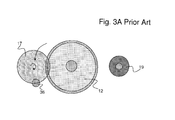
- FIG. 3A and 3B A Prior Art configuration of the anode vessel 19 and a separate reactive gas source 36 is illustrated in Figure 3A and 3B .
- the cathode 12 is positioned with its center at the central rotational axis C.
- An anode vessel 19 providing an ionized source of Argon gas is disposed on one side of the cathode 12 and the reactive gas source 36 of ionized Oxygen is disposed on an opposite side of the cathode 12.
- a substrate 17 rotates about the circumference of the cathode 12 over the reactive gas source 36.
- reactive sputtering with a standard cathode 12 a large variation of target wear has been observed which limits the target utilization.
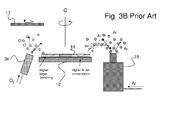
- the target 14 can be seen in the cross section in Figure 3B , on the side close to the reactive gas (oxidation) source 36, the target wear is low, due to an increase of target oxidation (poisoning); whereas on the side that is close to the anode 19, the target wear is high, due to an increase in plasma density.
- a simpler, less expensive and more reliable source for activated reactive gas in a magnetron sputtering device is highly desirable.
- the present invention has found that by integrating an anode vessel with a source for reactive gas, an activated reactive species can be provided in a magnetron sputtering device for applying dielectric coatings in a simpler, more efficient and cost effective device.
- the present invention comprises an integrated anode and activated reactive gas source, for use in a magnetron sputtering device comprising a vessel including:
- the present invention has a voltage provided to the anode comprising the interior conductive surface of the vessel of 15 to 80 Volts.
- the present invention includes the sputtering gas and reactive gas provided through a single inlet port into the vessel.
- the present invention includes the sputtering gas and reactive gas provided through separate inlet ports into the vessel.
- the present invention further comprises a magnetron sputtering device for coating objects including the integrated anode and activated reactive gas source in accordance with the present invention further comprising:
- magenetron sputtering device in accordance with the present invention wherein a distance from a surface plane of the objects to be coated to a plane containing the single opening of the vessel is equal to or greater than a distance from the surface plane of the objects to be coated to a surface plane of the target.
- the magnetron sputtering device in accordance with the present invention wherein two or more vessels comprising integrated anode and activated reactive gas sources are disposed at substantially opposite positions adjacent the cathode.
- the magnetron sputtering device in accordance with the present invention including a further reactive gas source to augment the integrated anode and activated reactive gas source.
- the magnetron sputtering device in accordance with the present invention wherein the two integrated anode and activated reactive gas sources operate continuously in operation.
- the magnetron sputtering device in accordance with the present invention wherein the two integrated anode and activated reactive gas sources operate intermittently, alternating between them at a frequency of 1 Hz or greater.
- Figure 1 is an isometric view of the coating system of the present invention with some outer wall removed;
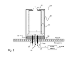
- Figure 2 is a cross-section of an anode vessel for use in the magnetron sputtering device
- Figure 3A is a schematic top view of a Prior Art separate anode vessel and activated reactive gas source
- Figure 3B is a schematic cross-section of the Prior Art separate anode vessel and activated reactive gas source
- Figure 4A is a schematic top view of a coating geometry in accordance with the present invention including an integrated anode and activated reactive gas source;
- Figure 4B is a schematic cross-section of the coating geometry of Figure 4A ;
- Figure 5A is a schematic top view of an alternative coating geometry in accordance with the present invention, in which the substrates to be coated pass over the cathode;
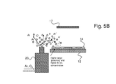
- Figure 5B is a schematic cross-section of the coating geometry of Figure 5A ;
- Figure 6A is a schematic top view of a coating geometry in accordance with the present invention in which the integrated anode and activated reactive gas source is disposed at the center of a ring shaped cathode;
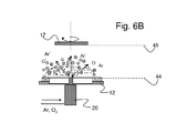
- Figure 6B is a schematic cross-section of the coating geometry of Figure 6A ;
- Figure 7A is a schematic top view of a coating geometry in accordance with the present invention in which two integrated anode and activated reactive gas sources are incorporated; and,
- Figure 7B is a schematic cross-section of the coating geometry of Figure 7A .
- the anode vessel disclosed in US Publication No. 20060049041 filed March 7, 2005 in its typical arrangement contains a plasma.
- the plasma is ignited by the high density of electrons coming from the cathode 12 and returning to the power supply through the anode 20.
- FIG. 1 An isometric view of the coating chamber 2 of a magnetron sputter coating device 10 is shown in Fig. 1 .
- Pumps 8 evacuate the coating chamber 2 for operation under vacuum conditions, understood to mean where the pressure is below atmospheric pressure.
- the chamber walls 32 are grounded and isolated from the positively charged anode 20 and the negatively charged cathode 12.
- a planetary drive 14 comprises a carrier 16 or rack rotatable about a central rotational axis C, with a plurality of eg. seven or eight, planets 17 supported radially about the central rotational axis C.
- a ring shaped cathode 12, in this embodiment two cathodes 12, are shown.
- Vessel 20 1 comprises an integrated anode and activated reactive gas source with an opening in communication with the coating chamber 2.
- Reference numerals 20 1 and 20 2 distinguish different positions of the integrated anode and activated reactive gas source 20.
- An additional integrated anode and activated reactive gas source 20 2 is shown at the center of cathode 12. These positions can be alternative positions, depending on whether a ring cathode or a solid cathode is used, or both can be used as shown. Even in the absence of a ring cathode, two integrated anode and activated reactive gas sources 20 can be positioned on opposite sides of a cathode, as shown in Figures 7A and B , to enable a higher deposition rate.
- the integrated anode and activated reactive gas source 20 includes one or more inlet ports 29 to supply sputter gas and reactive gas to the coating chamber 2.
- the magnetron sputter coating device 10 includes a load lock 1 for loading and unloading substrates or other objects 23, for coating. This allows the deposition chamber 2 to remain under vacuum conditions at all times.
- the integrated anode and activated reactive source can be implemented in a pulsed DC magnetron sputtering, DC magnetron, AC magnetron sputtering and rf magnetron sputtering.
- the integrated anode and activated reactive gas source 20 provides a charge differential to the negatively charged cathode.
- an integrated anode and activated reactive gas source 20 is shown in the form of a container or vessel having inner conductive surface of copper or stainless steel 22 comprising the anode and having a single opening 21 at a first end for communicating with a vacuum chamber 2 to which it is directly coupled.
- the opening 21 can be located on a side or end of the vessel. Conveniently, the opening 21 can be positioned in the chamber walls 32 with the vessel itself outside the chamber 2. This achieves space efficiency in the chamber and assists service access.
- the opening 21 is positioned adjacent the cathode 12 approximately positioning the plume of sputtered material from the target and the plume of activated and ionized oxygen to overlap as closely as possible to simultaneously arrive at the substrate to be coated.
- the outer surface 26 of the vessel 20 is electrically insulated.
- water cooling pipes 28 are shown substantially around the anode 20 for maintaining the temperature of the anode in operation.
- a gas inlet port 29 is shown for providing a conduit into which sputter gas and reactive gas, Oxygen or Nitrogen, may enter the vessel 20. The gasses are mixed prior to the inlet port 29, or alternately two separate inlet ports 29 can be coupled into the vessel 20.
- the flow of reactive gas can be shut off when the coating device 10 is not creating dielectric coatings, so that only sputter gas flows through the vessel 20.
- the size of the opening 21 is relatively small and the flow of gases can be selected to locally pressurize the vessel 20.
- the relatively small opening 21, having a circumference significantly smaller than the circumference of the vessel, and the location of the opening 21 out of a line of sight to the target prevent coating material from entering and coating the inner conductive surface 22 of the anode.
- the vessel 20 is pressurized above the chamber pressure with the flow of argon gas and a reactive gas that together promote the formation of plasma in the coating chamber 2.
- a plasma is ignited by the high density of electrons coming from the cathode and returning to the power supply through the anode, and is sustained by a maintenance voltage thereafter.
- the argon plasma has proven to be sufficient to ignite the reactive gas simultaneously.
- Pressure within the vessel 20, higher than the rest of the vacuum coating chamber 2 allows for a lower anode voltage that promotes a more stable sputtering condition.
- Positive power supply lead 25 connects the power supply to the inner conductive surface 22 of the anode.
- the integrated anode and activated reactive gas source device 20 shown in Figure 2 was designed to function with a low anode voltage and little or no arcing. A low anode voltage of approximately +15 to +80 volts is preferred to reduce process variation.
- the anode inner conductive surface 22 are electrically insulated from the grounded chamber walls 32 by an insulating material 33.
- the chamber pressure is below 0.267 Pa (2 mTorr.)
- a higher pressure at the anode is achieved by the smaller opening 21 of the anode 20 and a controlled flow of process gas and reactive gas into the vessel 20 via the inlet port 29.
- An optimum opening has an area of about 20cm 2 and is preferably round.
- the vessel 20 can be pressurized to more than 0.400 Pa (3mTorr.)
- a cathode 12 is disposed with its center at the central axis C.
- the integrated anode and activated reactive gas source 20 is located adjacent the cathode 12.
- At least one substrate 17 mounted to a coating area is rotated about an orbit of the central axis C at a radial distance substantially equal to the distance of the integrated anode and activated reactive gas source 20 from the central axis C, so that the at least one substrate 17 passes over the opening 21 of the integrated anode and activated reactive gas source.
- FIG. 5A and 5B In another configuration of a magnetron sputtering device incorporating an integrated anode and activated reactive gas source, shown in Figures 5A and 5B the cathode 12 is translated a radial distance from the central axis C. One or more substrates 17 are rotated in an orbit having a radius equal to the radial distance the cathode 12 is translated.
- the integrated anode and activated reactive gas source 20 is also located a same radial distance from the center adjacent the cathode 12, so that the one or more substrates 17 pass over the cathode 12 and integrated anode and activated reactive gas source 20 in quick succession.
- An integrated anode and activated reactive gas source 20 can be located with its opening 21 at the center of the ring cathode in a magnetron sputtering device, as shown in Figure 1 and Figure 6 , since the opening 21 is relatively far away from strong magnetic fields. This improves the symmetry of the system, which is expected to cause a uniform wear pattern of the target, which improves target utilization.
- auxiliary activated reactive source located a distance from the cathode 12 (eg. at 20 1 as shown in Fig. 1 ) can be provided in addition to enable a higher deposition rate.
- higher deposition rates of metal oxides with low absorption can be achieved when the plume of sputtered material from the target and the plume of activated and ionized oxygen overlap and simultaneously arrive at the substrate to be coated.
- the source output can be ionized, or otherwise activated oxygen species (e.g. atomic oxygen, ozone).
- the opening 21 of the integrated anode and activated reactive gas source 20 is positioned just at a target surface plane 44 in the center of the cathode 12.
- Substrates 17 are supported for rotation over the concentric cathode 12 and integrated anode and activated reactive gas source 20.
- a distance from a surface plane 46 of the objects to be coated to a plane containing the single opening 21 of the vessel 20 is equal to or greater than a distance from the surface plane of the objects to be coated to a surface plane of the target.
- FIG. 7A and 7B A further example configuration of a magnetron sputtering device incorporating and integrated anode and activated reactive gas source is shown in Figures 7A and 7B in which two integrated anode and activated reactive gas source vessels 20 are disposed on opposite sides of a cathode 12, each vessel 20 and the cathode located a same radial distance from a central rotation axis C.
- a support for one or more substrates to be coated is adapted to support the substrates in a rotation about the central rotation axis C the same radial distance so as to pass the substrates above the cathode and integrated anode and activated reactive gas sources.
- the two integrated anode and activated reactive gas sources 20 can be used both continuously, or cycled alternately between them at a frequency of 1 Hz or greater.
Landscapes
- Chemical & Material Sciences (AREA)
- Engineering & Computer Science (AREA)
- Chemical Kinetics & Catalysis (AREA)
- Materials Engineering (AREA)
- Mechanical Engineering (AREA)
- Metallurgy (AREA)
- Organic Chemistry (AREA)
- Physics & Mathematics (AREA)
- Plasma & Fusion (AREA)
- Analytical Chemistry (AREA)
- Physical Vapour Deposition (AREA)
- Plasma Technology (AREA)
Abstract
Description
- This invention relates generally to a magnetron sputtering device for depositing materials onto substrates. More particularly the invention relates to an integrated anode and activated reactive gas source for use in a magnetron sputtering device and a magnetron sputtering device incorporating the same.
- Sputter coating is a widely used technique for depositing a thin film of material on a substrate. In a sputtering deposition process ions are usually created by collisions between gas atoms and electrons in a glow discharge. The ions are accelerated into the target of coating material at the cathode by an electric field causing atoms of the target material to be ejected from the target surface. A substrate is placed in a suitable location so that it intercepts a portion of the ejected atoms. Thus, a coating of target material is deposited on the surface of the substrate. In reactive sputtering a gaseous species is also present at the substrate surface and reacts with, and in some embodiments combines with, the atoms from the target surface to form the desired coating material.
- In operation, when the sputter gas, e.g. argon, is admitted into a coating chamber, a DC voltage applied between the cathode and the anode ionizes the argon into a plasma, and the positively charged argon ions are attracted to the negatively charged cathode. The ions strike the target in front of the cathode with a substantial energy and cause target atoms or atomic clusters to be sputtered from the target. Some of the target particles strike and deposit on the wafer or substrate material to be coated, thereby forming a film.
- To attain increased deposition rates and lower operating pressures, magnetically enhanced cathodes are used. In a planar magnetron, the cathode includes an array of permanent magnets arranged in a closed loop and mounted in a fixed position in relation to the flat target plate of coating material. Thus, the magnetic field causes the electrons to travel in a closed loop, commonly referred to as a "race track", which establishes the path or region along which sputtering or erosion of the target material takes place. In a magnetron cathode, a magnetic field confines the glow discharge plasma and increases the path length of the electrons moving under the influence of the electric field. This results in an increase in the gas atom-electron collision probability, thereby leading to a much higher sputtering rate than that obtained without the use of magnetic confinement. Furthermore, the sputtering process can be accomplished at a much lower gas pressure.
- Typically a magnetron sputtering system is operated at a pressure of 2* 10^-2 Pa-1*10^-1 Pa. during sputtering. To establish this pressure, typically the chamber is pumped down to a pressure of <1*10^-4 Pa. and a controlled flow of a gas, typically Argon (and in case of reactive sputtering Argon and Oxygen or Nitrogen) is fed into the chamber to maintain the desired pressure. In the case of a diode system, i.e. when no magnets are used, a pressure of >2Pa. is required to be able to ignite and sustain a plasma. High pressure has the disadvantage that the mean-free path is greatly reduced, which causes extensive gas scatter. This results in hazy coatings.
- In the magnetron sputtering device the anode provides a charge differential to the negatively charged cathode. This can be provided as simply as an electric charge provided to the chamber walls. However, the sputtered material is also deposited on any surface exposed to the sputtered atoms. If the coating is an electrically insulating material, such as a metal oxide, the build up of the material on other parts of the sputtering apparatus can cause problems. In particular, the build up of an insulating coating on the anode interferes with the ability of the anode to remove electrons from the plasma, as required to maintain the plasma's charge balance. This destabilizes the plasma and interferes with deposition control. Coating build-up will cause the anode location to move to another surface in the system. This instability affects coating quality. Numerous prior art anodes have been proposed to overcome the problems of the anode becoming coated with the coating material. Many prior art anodes function at very high voltages that also increase the problems of arcing, which damages coating quality. A low voltage anode that can provide a stable anode location is desired for ensuring consistent coating quality.
- An anode vessel is disclosed in
US Publication No. 20060049041 filed March 7, 2005 that can provide a stable anode location at low voltage. The anode comprises an interior surface of a vessel having a single opening in communication with the coating chamber. The interior surface of the vessel is the preferred return path for electrons. The anode vessel is also the source of sputter gas, which passes from an inlet port in the anode vessel through the single opening into the coating chamber. The size of the single opening and its location prevent coating material from building up on the charged interior surface of the anode. - Many optical coatings require the deposition of oxides or other compounds. Such materials are preferably produced in reactive sputter mode where a metallic target is sputtered and oxygen, nitrogen, or another reactive gas is added to the process. The sputtered material and the activated oxygen species arrive simultaneously at the substrate. The optimum flow, of oxygen for example, for the optimum oxygen partial pressure needs to be found. If the oxygen flow is too low, the films are not stoichiometric and have high absorption losses. If it is too high, the target surface becomes more oxidized than necessary preventing operation at the highest possible deposition rate. The sputter rate for a metallic target can be ten times higher than that of a fully oxidized target. The oxidation effectiveness can be increased if the oxygen is activated and directed at the substrates, thus increasing the possible deposition rate. The reactive sputter process is disclosed for oxides. All aspects can similarly be applied to nitrides or other reactive processes.
- In order to produce dielectric coatings in a magnetron sputtering device with low or no optical absorption profile, it is necessary to provide an additional activated reactive gas source to provide Oxygen or Nitrogen to create a plasma. Examples of commercially available activated reactive gas sources include a PAS from JDSU, a Taurion source from ProVac, a KRI source from Kaufman & Robinson, an APS source from Leybold. Current activated reactive gas sources are complicated. Some require expensive electronics. Some require filaments that have limited lifetime. These devices are very expensive and can be maintenance intensive.
- A Prior Art configuration of the
anode vessel 19 and a separatereactive gas source 36 is illustrated inFigure 3A and3B . Thecathode 12 is positioned with its center at the central rotational axis C. Ananode vessel 19 providing an ionized source of Argon gas is disposed on one side of thecathode 12 and thereactive gas source 36 of ionized Oxygen is disposed on an opposite side of thecathode 12. Asubstrate 17 rotates about the circumference of thecathode 12 over thereactive gas source 36. In the case of reactive sputtering with astandard cathode 12, a large variation of target wear has been observed which limits the target utilization. Thetarget 14 can be seen in the cross section inFigure 3B , on the side close to the reactive gas (oxidation)source 36, the target wear is low, due to an increase of target oxidation (poisoning); whereas on the side that is close to theanode 19, the target wear is high, due to an increase in plasma density. - A simpler, less expensive and more reliable source for activated reactive gas in a magnetron sputtering device is highly desirable.
- It is also desired to increase the efficiency of oxidation of the deposited film in order to increase the deposition rate for reactive sputtering.
- It is also desired to maintain a low temperature process despite increased power input in order to be able to process temperature sensitive materials.
- The present invention has found that by integrating an anode vessel with a source for reactive gas, an activated reactive species can be provided in a magnetron sputtering device for applying dielectric coatings in a simpler, more efficient and cost effective device.
- Accordingly, the present invention comprises an integrated anode and activated reactive gas source, for use in a magnetron sputtering device comprising a vessel including:
- an interior conductive surface of the vessel, adapted to be electrically coupled to a positive output of a power supply, comprising the anode for providing a voltage difference to a cathode such that the anode is the primary return path for electrons,
- a single opening for communication with a coating chamber of the magnetron sputtering device;
- an insulated outer surface of the vessel electrically isolated from chamber walls of the coating chamber;
- a source for sputtering gas coupled into the vessel for providing sputtering gas through the single opening into the coating chamber; and
- a source for reactive gas coupled into the vessel for providing reactive gas through the single opening into the coating chamber.
- The present invention has a voltage provided to the anode comprising the interior conductive surface of the vessel of 15 to 80 Volts.
- The present invention includes the sputtering gas and reactive gas provided through a single inlet port into the vessel.
- The present invention includes the sputtering gas and reactive gas provided through separate inlet ports into the vessel.
- The present invention further comprises a magnetron sputtering device for coating objects including the integrated anode and activated reactive gas source in accordance with the present invention further comprising:
- a coating chamber adapted to be evacuated in operation;
- a cathode including a target comprising material for forming a coating; and one or more coating areas having supports to support objects to be coated within a coating area in the coating chamber.
- The magenetron sputtering device in accordance with the present invention wherein a distance from a surface plane of the objects to be coated to a plane containing the single opening of the vessel is equal to or greater than a distance from the surface plane of the objects to be coated to a surface plane of the target.
- The magnetron sputtering device in accordance with the present invention, wherein two or more vessels comprising integrated anode and activated reactive gas sources are disposed at substantially opposite positions adjacent the cathode.
- The magnetron sputtering device in accordance with the present invention, including a further reactive gas source to augment the integrated anode and activated reactive gas source.
- The magnetron sputtering device in accordance with the present invention, wherein the two integrated anode and activated reactive gas sources operate continuously in operation.
- The magnetron sputtering device in accordance with the present invention, wherein the two integrated anode and activated reactive gas sources operate intermittently, alternating between them at a frequency of 1 Hz or greater.
- Exemplary embodiments of the invention will now be described in accordance with the drawings, in which:
-
Figure 1 is an isometric view of the coating system of the present invention with some outer wall removed; -
Figure 2 is a cross-section of an anode vessel for use in the magnetron sputtering device; -
Figure 3A is a schematic top view of a Prior Art separate anode vessel and activated reactive gas source; -
Figure 3B is a schematic cross-section of the Prior Art separate anode vessel and activated reactive gas source; -
Figure 4A is a schematic top view of a coating geometry in accordance with the present invention including an integrated anode and activated reactive gas source; -
Figure 4B is a schematic cross-section of the coating geometry ofFigure 4A ; -
Figure 5A is a schematic top view of an alternative coating geometry in accordance with the present invention, in which the substrates to be coated pass over the cathode; -
Figure 5B is a schematic cross-section of the coating geometry ofFigure 5A ; -
Figure 6A is a schematic top view of a coating geometry in accordance with the present invention in which the integrated anode and activated reactive gas source is disposed at the center of a ring shaped cathode; -
Figure 6B is a schematic cross-section of the coating geometry ofFigure 6A ; -
Figure 7A is a schematic top view of a coating geometry in accordance with the present invention in which two integrated anode and activated reactive gas sources are incorporated; and, -
Figure 7B is a schematic cross-section of the coating geometry ofFigure 7A . - We observed that the anode vessel disclosed in
US Publication No. 20060049041 filed March 7, 2005 in its typical arrangement contains a plasma. The plasma is ignited by the high density of electrons coming from thecathode 12 and returning to the power supply through theanode 20. The effect of ion creation and the creation of activated species is similar to the reactions occurring at the cathode: energetic e- + Ar =≥ 2e- + Ar+ or energetic e- + Ar => e- + Ar*. There would not be visible plasma at the anode without this activation of the argon atoms. We decided to test adding oxygen to the anode to test if it would generate activated and ionized oxygen. By coupling the oxygen feed into theanode vessel 20, we were able to deposit a clear SiO2 single layer. This is a clear indication that the anode operating with argon and oxygen is behaving as an anode and an activated reactive gas source. Additionally, we did not observe oxidation of the inside walls of the anode. - An isometric view of the
coating chamber 2 of a magnetronsputter coating device 10 is shown inFig. 1 .Pumps 8 evacuate thecoating chamber 2 for operation under vacuum conditions, understood to mean where the pressure is below atmospheric pressure. Thechamber walls 32 are grounded and isolated from the positively chargedanode 20 and the negatively chargedcathode 12. Aplanetary drive 14 comprises a carrier 16 or rack rotatable about a central rotational axis C, with a plurality of eg. seven or eight,planets 17 supported radially about the central rotational axis C. A ring shapedcathode 12, in this embodiment twocathodes 12, are shown.Vessel 201 comprises an integrated anode and activated reactive gas source with an opening in communication with thecoating chamber 2.Reference numerals reactive gas source 20. An additional integrated anode and activatedreactive gas source 202 is shown at the center ofcathode 12. These positions can be alternative positions, depending on whether a ring cathode or a solid cathode is used, or both can be used as shown. Even in the absence of a ring cathode, two integrated anode and activatedreactive gas sources 20 can be positioned on opposite sides of a cathode, as shown inFigures 7A andB , to enable a higher deposition rate. The integrated anode and activated reactive gas source 20 (seeFigure 2 ) includes one ormore inlet ports 29 to supply sputter gas and reactive gas to thecoating chamber 2. The magnetronsputter coating device 10 includes aload lock 1 for loading and unloading substrates orother objects 23, for coating. This allows thedeposition chamber 2 to remain under vacuum conditions at all times. - The integrated anode and activated reactive source can be implemented in a pulsed DC magnetron sputtering, DC magnetron, AC magnetron sputtering and rf magnetron sputtering.
- The integrated anode and activated
reactive gas source 20 provides a charge differential to the negatively charged cathode. Referring now toFigure 2 an integrated anode and activatedreactive gas source 20 is shown in the form of a container or vessel having inner conductive surface of copper orstainless steel 22 comprising the anode and having asingle opening 21 at a first end for communicating with avacuum chamber 2 to which it is directly coupled. Theopening 21 can be located on a side or end of the vessel. Conveniently, theopening 21 can be positioned in thechamber walls 32 with the vessel itself outside thechamber 2. This achieves space efficiency in the chamber and assists service access. Theopening 21 is positioned adjacent thecathode 12 approximately positioning the plume of sputtered material from the target and the plume of activated and ionized oxygen to overlap as closely as possible to simultaneously arrive at the substrate to be coated. Theouter surface 26 of thevessel 20 is electrically insulated. In the cross sectional viewwater cooling pipes 28 are shown substantially around theanode 20 for maintaining the temperature of the anode in operation. Agas inlet port 29 is shown for providing a conduit into which sputter gas and reactive gas, Oxygen or Nitrogen, may enter thevessel 20. The gasses are mixed prior to theinlet port 29, or alternately twoseparate inlet ports 29 can be coupled into thevessel 20. The flow of reactive gas can be shut off when thecoating device 10 is not creating dielectric coatings, so that only sputter gas flows through thevessel 20. The size of theopening 21 is relatively small and the flow of gases can be selected to locally pressurize thevessel 20. The relativelysmall opening 21, having a circumference significantly smaller than the circumference of the vessel, and the location of theopening 21 out of a line of sight to the target prevent coating material from entering and coating the innerconductive surface 22 of the anode. In operation thevessel 20 is pressurized above the chamber pressure with the flow of argon gas and a reactive gas that together promote the formation of plasma in thecoating chamber 2. A plasma is ignited by the high density of electrons coming from the cathode and returning to the power supply through the anode, and is sustained by a maintenance voltage thereafter. The argon plasma has proven to be sufficient to ignite the reactive gas simultaneously. Pressure within thevessel 20, higher than the rest of thevacuum coating chamber 2, allows for a lower anode voltage that promotes a more stable sputtering condition. Positivepower supply lead 25 connects the power supply to the innerconductive surface 22 of the anode. The integrated anode and activated reactivegas source device 20 shown inFigure 2 was designed to function with a low anode voltage and little or no arcing. A low anode voltage of approximately +15 to +80 volts is preferred to reduce process variation. The anode innerconductive surface 22 are electrically insulated from the groundedchamber walls 32 by an insulatingmaterial 33. - In a preferred embodiment the integrated anode and activated reactive gas source comprises a vessel of cylindrical shape with a diameter of at least d = 10 cm and a length of at least h = 20 cm with an opening (21) to the vacuum chamber (2) at one end as shown in
Figure 2 and closed at the opposite end. For low scattering processes the chamber pressure is below 0.267 Pa (2 mTorr.) A higher pressure at the anode is achieved by thesmaller opening 21 of theanode 20 and a controlled flow of process gas and reactive gas into thevessel 20 via theinlet port 29. An optimum opening has an area of about 20cm2 and is preferably round. In operation thevessel 20 can be pressurized to more than 0.400 Pa (3mTorr.) - In one configuration of a magnetron sputtering device incorporating an integrated anode and activated reactive gas source, shown in
Figures 4A and4B , acathode 12 is disposed with its center at the central axis C. The integrated anode and activatedreactive gas source 20 is located adjacent thecathode 12. At least onesubstrate 17 mounted to a coating area is rotated about an orbit of the central axis C at a radial distance substantially equal to the distance of the integrated anode and activatedreactive gas source 20 from the central axis C, so that the at least onesubstrate 17 passes over the opening 21 of the integrated anode and activated reactive gas source. One would expect a lower gradient of target wear in this configuration than inFigure 3A ,B , because higher plasma density (high Ar ion concentration) and poisoning of the target are at the same location. - In another configuration of a magnetron sputtering device incorporating an integrated anode and activated reactive gas source, shown in
Figures 5A and5B thecathode 12 is translated a radial distance from the central axis C. One ormore substrates 17 are rotated in an orbit having a radius equal to the radial distance thecathode 12 is translated. The integrated anode and activatedreactive gas source 20 is also located a same radial distance from the center adjacent thecathode 12, so that the one ormore substrates 17 pass over thecathode 12 and integrated anode and activatedreactive gas source 20 in quick succession. - An integrated anode and activated
reactive gas source 20 can be located with itsopening 21 at the center of the ring cathode in a magnetron sputtering device, as shown inFigure 1 andFigure 6 , since theopening 21 is relatively far away from strong magnetic fields. This improves the symmetry of the system, which is expected to cause a uniform wear pattern of the target, which improves target utilization. - In a preferred embodiment shown in
Figures 6A and6B , by including the oxygen source in the anode vessel together as an integrated anode and activatedreactive gas source 20 in the center of thecathode 12, a very symmetric system is created and target wear is expected to be uniform. An auxiliary activated reactive source located a distance from the cathode 12 (eg. at 201 as shown inFig. 1 ) can be provided in addition to enable a higher deposition rate. Experiments have shown that higher deposition rates of metal oxides with low absorption can be achieved when the plume of sputtered material from the target and the plume of activated and ionized oxygen overlap and simultaneously arrive at the substrate to be coated. Thus, having the integrated anode and activatedreactive gas source 20 in the center of the target is an almost ideal solution. The source output can be ionized, or otherwise activated oxygen species (e.g. atomic oxygen, ozone). Theopening 21 of the integrated anode and activatedreactive gas source 20 is positioned just at atarget surface plane 44 in the center of thecathode 12.Substrates 17 are supported for rotation over theconcentric cathode 12 and integrated anode and activatedreactive gas source 20. A distance from asurface plane 46 of the objects to be coated to a plane containing thesingle opening 21 of thevessel 20 is equal to or greater than a distance from the surface plane of the objects to be coated to a surface plane of the target. - A further example configuration of a magnetron sputtering device incorporating and integrated anode and activated reactive gas source is shown in
Figures 7A and7B in which two integrated anode and activated reactivegas source vessels 20 are disposed on opposite sides of acathode 12, eachvessel 20 and the cathode located a same radial distance from a central rotation axis C. A support for one or more substrates to be coated, is adapted to support the substrates in a rotation about the central rotation axis C the same radial distance so as to pass the substrates above the cathode and integrated anode and activated reactive gas sources. The two integrated anode and activatedreactive gas sources 20 can be used both continuously, or cycled alternately between them at a frequency of 1 Hz or greater. - Numerous other configurations for use in different magnetron platforms, such as in-line or with rectangular or cylindrical cathodes are also feasible.
Claims (15)
- An integrated anode and activated reactive gas source (20), for use in a magnetron sputtering device (10) comprising a vessel including:an interior conductive surface (22) of the vessel, adapted to be electrically coupled to a positive output of a power supply, comprising the anode for providing a voltage difference to a cathode (12) such that the anode is the primary return path for electrons,a single opening (21) for communication with a coating chamber (2) of the magnetron sputtering device (10);an insulated outer surface (26) of the vessel electrically isolated from chamber walls (32) of the coating chamber (2);a source for sputtering gas (29) coupled into the vessel for providing sputtering gas through the single opening (21) into the coating chamber (2); characterized in that the vessel also includes:a source for reactive gas (29) coupled into the vessel for providing reactive gas through the single opening (21) into the coating chamber (2).
- The integrated anode and activated reactive gas source defined in claim 1, wherein the single opening (21) is smaller than a circumference of the vessel to shield the interior conductive surface (22) from most sputtered material.
- The integrated anode and activated reactive gas source defined in claim 2, wherein the single opening (21) is dimensioned such that the flow of sputter gas and reactive gas can be selected to raise the pressure locally within the vessel higher than a pressure in the coating chamber (2).
- The integrated anode and activated reactive gas source defined in claim 3, wherein the voltage provided to the anode comprising the interior conductive surface (22) of the vessel is 15 to 80 Volts.
- The integrated anode and activated reactive gas source defined in claim 4, wherein the sputtering gas and reactive gas are provided through a single inlet port into the vessel.
- The integrated anode and activated reactive gas source defined in claim 4, wherein the sputtering gas and reactive gas are provided through separate inlet ports into the vessel.
- A magnetron sputtering device (10) for coating objects including the integrated anode and activated reactive gas source (20) defined in claim 4, further comprising:a coating chamber (2) adapted to be evacuated in operation;a cathode (12) including a target (14) comprising material for forming a coating; and one or more coating areas (17) having supports to support objects to be coated within a coating area in the coating chamber (2).
- The magenetron sputtering device defined in claim 7, wherein a distance from a surface plane of the objects to be coated (46) to a plane containing the single opening of the vessel (21) is equal to or greater than a distance from the surface plane of the objects to be coated (46) to a surface plane of the target (44).
- The magnetron sputtering device defined in claim 8, wherein two or more vessels comprising integrated anode and activated reactive gas sources (20) are disposed at substantially opposite positions adjacent the cathode (12).
- The magnetron sputtering device defined in claim 8, including a further reactive gas source (36) to augment the integrated anode and activated reactive gas source (20).
- The magnetron sputtering device as defined in claim 8, wherein the one or more coating areas (17) are adapted to rotate about a central rotational axis coincident with a center point of the cathode, and the coating areas (17) and the integrated anode and activated reactive gas source (20) are disposed a same radial distance from the central rotational axis, such that in operation the coating areas (17) pass directly above the single opening of the vessel (21).
- The magnetron sputtering device as defined in claim 8, wherein the cathode (12) and integrated anode and activated reactive gas source (20) are disposed adjacent each other at a radial distance from a central rotational axis, and the coating areas (17) are adapted to rotate at a same radial distance from the central rotational axis, such that in operation the coating areas (17) pass directly over the cathode (12) and the integrated anode and activated reactive gas source (20).
- The magnetron sputtering device as defined in claim 8, wherein the cathode (12) is disposed a radial distance from a central rotational axis and two integrated anode and activated reactive gas sources (20) are disposed a same radial distance from the central rotational axis on either side of the cathode (12), the coating areas (17) are adapted to rotate about the central rotational axis at a same radial distance as the cathode (12) and integrated anode and activated reactive gas sources (20), such that in operation the coating areas (17) pass directly over the cathode (12) and the integrated anode and activated reactive gas sources (20).
- The magnetron sputtering device as defined in claim 13, wherein the two integrated anode and activated reactive gas sources (20) operate continuously in operation.
- The magnetron sputtering device as defined in claim 13, wherein the two integrated anode and activated reactive gas sources (20) operate intermittently, alternating between them at a frequency of 1 Hz or greater.
Applications Claiming Priority (1)
| Application Number | Priority Date | Filing Date | Title |
|---|---|---|---|
| US201161472494P | 2011-04-06 | 2011-04-06 |
Publications (3)
| Publication Number | Publication Date |
|---|---|
| EP2509100A2 true EP2509100A2 (en) | 2012-10-10 |
| EP2509100A3 EP2509100A3 (en) | 2014-05-28 |
| EP2509100B1 EP2509100B1 (en) | 2019-08-14 |
Family
ID=44872190
Family Applications (1)
| Application Number | Title | Priority Date | Filing Date |
|---|---|---|---|
| EP11183181.4A Active EP2509100B1 (en) | 2011-04-06 | 2011-09-28 | Integrated anode and activated reactive gas source for use in a magnetron sputtering device |
Country Status (4)
| Country | Link |
|---|---|
| EP (1) | EP2509100B1 (en) |
| JP (3) | JP5951210B2 (en) |
| CN (2) | CN105349955B (en) |
| DK (1) | DK2509100T3 (en) |
Cited By (3)
| Publication number | Priority date | Publication date | Assignee | Title |
|---|---|---|---|---|
| EP3340274A1 (en) * | 2016-12-24 | 2018-06-27 | WINDLIPIE spólka z ograniczona odpowiedzialnoscia spólka komandytowa | Magnetron sputtering device |
| US20240194464A1 (en) * | 2022-12-09 | 2024-06-13 | Intevac, Inc. | Stable ground anode for thin film processing |
| US12542263B2 (en) | 2022-12-12 | 2026-02-03 | Intevac, Inc. | Cylindrical cathode and chamber using same for sputtering |
Families Citing this family (5)
| Publication number | Priority date | Publication date | Assignee | Title |
|---|---|---|---|---|
| CN111491713B (en) * | 2017-10-18 | 2022-07-15 | 乔瓦尼·巴尔科 | Method and apparatus for generating active clusters of oxygen and/or nitrogen in liquid solution or in gaseous form |
| EP4073830A1 (en) * | 2019-12-13 | 2022-10-19 | Evatec AG | Gas ring for a pvd source |
| CN111791022A (en) * | 2020-06-01 | 2020-10-20 | 肇庆宏旺金属实业有限公司 | Processing method of snowflake sand wire drawing surface super black steel stainless steel plate |
| JP7581953B2 (en) * | 2021-02-24 | 2024-11-13 | 東京エレクトロン株式会社 | Apparatus and method for performing sputtering process |
| JP2023016004A (en) * | 2021-07-20 | 2023-02-01 | キヤノン株式会社 | Sputtering apparatus, film forming method, and article manufacturing method |
Citations (1)
| Publication number | Priority date | Publication date | Assignee | Title |
|---|---|---|---|---|
| US20060049041A1 (en) | 2004-08-20 | 2006-03-09 | Jds Uniphase Corporation | Anode for sputter coating |
Family Cites Families (8)
| Publication number | Priority date | Publication date | Assignee | Title |
|---|---|---|---|---|
| DE3521053A1 (en) * | 1985-06-12 | 1986-12-18 | Leybold-Heraeus GmbH, 5000 Köln | DEVICE FOR APPLYING THIN LAYERS TO A SUBSTRATE |
| US5855745A (en) * | 1997-04-23 | 1999-01-05 | Sierra Applied Sciences, Inc. | Plasma processing system utilizing combined anode/ ion source |
| JP2000226652A (en) * | 1998-12-04 | 2000-08-15 | Sanyo Shinku Kogyo Kk | Thin film manufacturing method and apparatus |
| JP2002069632A (en) * | 2000-09-05 | 2002-03-08 | Canon Inc | Sputtering apparatus and sputtering method |
| DE102004014855A1 (en) * | 2004-03-26 | 2004-10-21 | Applied Films Gmbh & Co. Kg | Device for reactive sputtering comprises a controllable valve to control the total gas flow into a sputtering chamber, and a control unit for keeping the ratio of the partial pressures of at least two gases constant |
| US7879209B2 (en) * | 2004-08-20 | 2011-02-01 | Jds Uniphase Corporation | Cathode for sputter coating |
| WO2007118204A2 (en) * | 2006-04-06 | 2007-10-18 | Applied Materials, Inc. | Reactive sputtering zinc oxide transparent conductive oxides onto large area substrates |
| JP5619666B2 (en) * | 2010-04-16 | 2014-11-05 | ジェイディーエス ユニフェイズ コーポレーションJDS Uniphase Corporation | Ring cathode for use in magnetron sputtering devices |
-
2011
- 2011-09-28 EP EP11183181.4A patent/EP2509100B1/en active Active
- 2011-09-28 DK DK11183181T patent/DK2509100T3/en active
- 2011-10-03 JP JP2011218940A patent/JP5951210B2/en active Active
- 2011-10-08 CN CN201510790668.5A patent/CN105349955B/en active Active
- 2011-10-08 CN CN201110304009.8A patent/CN102737950B/en active Active
-
2015
- 2015-12-23 JP JP2015250752A patent/JP6189406B2/en active Active
-
2017
- 2017-08-02 JP JP2017150021A patent/JP2017222931A/en active Pending
Patent Citations (1)
| Publication number | Priority date | Publication date | Assignee | Title |
|---|---|---|---|---|
| US20060049041A1 (en) | 2004-08-20 | 2006-03-09 | Jds Uniphase Corporation | Anode for sputter coating |
Cited By (3)
| Publication number | Priority date | Publication date | Assignee | Title |
|---|---|---|---|---|
| EP3340274A1 (en) * | 2016-12-24 | 2018-06-27 | WINDLIPIE spólka z ograniczona odpowiedzialnoscia spólka komandytowa | Magnetron sputtering device |
| US20240194464A1 (en) * | 2022-12-09 | 2024-06-13 | Intevac, Inc. | Stable ground anode for thin film processing |
| US12542263B2 (en) | 2022-12-12 | 2026-02-03 | Intevac, Inc. | Cylindrical cathode and chamber using same for sputtering |
Also Published As
| Publication number | Publication date |
|---|---|
| JP6189406B2 (en) | 2017-08-30 |
| CN102737950B (en) | 2016-05-04 |
| JP5951210B2 (en) | 2016-07-13 |
| DK2509100T3 (en) | 2019-11-04 |
| CN105349955A (en) | 2016-02-24 |
| EP2509100B1 (en) | 2019-08-14 |
| CN102737950A (en) | 2012-10-17 |
| JP2012219374A (en) | 2012-11-12 |
| CN105349955B (en) | 2018-07-17 |
| EP2509100A3 (en) | 2014-05-28 |
| JP2017222931A (en) | 2017-12-21 |
| JP2016104910A (en) | 2016-06-09 |
Similar Documents
| Publication | Publication Date | Title |
|---|---|---|
| EP2509100B1 (en) | Integrated anode and activated reactive gas source for use in a magnetron sputtering device | |
| CN102220561B (en) | Ring cathode for use in a magnetron sputtering device | |
| EP1554412B1 (en) | Plasma enhanced chemical vapor deposition apparatus | |
| US6361667B1 (en) | Ionization sputtering apparatus | |
| US7411352B2 (en) | Dual plasma beam sources and method | |
| WO2011131921A1 (en) | High density plasma source | |
| US20060070877A1 (en) | Magnetron sputtering device | |
| US20220181129A1 (en) | Magnetron plasma apparatus | |
| CN104011254B (en) | Continuous film-forming method of precious metal film and continuous manufacturing method of electronic parts | |
| US9502222B2 (en) | Integrated anode and activated reactive gas source for use in magnetron sputtering device | |
| HK1162619B (en) | Ring cathode for use in a magnetron sputtering device |
Legal Events
| Date | Code | Title | Description |
|---|---|---|---|
| PUAI | Public reference made under article 153(3) epc to a published international application that has entered the european phase |
Free format text: ORIGINAL CODE: 0009012 |
|
| AK | Designated contracting states |
Kind code of ref document: A2 Designated state(s): AL AT BE BG CH CY CZ DE DK EE ES FI FR GB GR HR HU IE IS IT LI LT LU LV MC MK MT NL NO PL PT RO RS SE SI SK SM TR |
|
| AX | Request for extension of the european patent |
Extension state: BA ME |
|
| PUAL | Search report despatched |
Free format text: ORIGINAL CODE: 0009013 |
|
| AK | Designated contracting states |
Kind code of ref document: A3 Designated state(s): AL AT BE BG CH CY CZ DE DK EE ES FI FR GB GR HR HU IE IS IT LI LT LU LV MC MK MT NL NO PL PT RO RS SE SI SK SM TR |
|
| AX | Request for extension of the european patent |
Extension state: BA ME |
|
| RIC1 | Information provided on ipc code assigned before grant |
Ipc: H01J 37/34 20060101AFI20140423BHEP Ipc: H01J 37/32 20060101ALI20140423BHEP Ipc: C23C 14/00 20060101ALI20140423BHEP |
|
| 17P | Request for examination filed |
Effective date: 20141016 |
|
| RBV | Designated contracting states (corrected) |
Designated state(s): AL AT BE BG CH CY CZ DE DK EE ES FI FR GB GR HR HU IE IS IT LI LT LU LV MC MK MT NL NO PL PT RO RS SE SI SK SM TR |
|
| RAP1 | Party data changed (applicant data changed or rights of an application transferred) |
Owner name: VIAVI SOLUTIONS INC. |
|
| RAP1 | Party data changed (applicant data changed or rights of an application transferred) |
Owner name: VIAVI SOLUTIONS INC. |
|
| GRAP | Despatch of communication of intention to grant a patent |
Free format text: ORIGINAL CODE: EPIDOSNIGR1 |
|
| STAA | Information on the status of an ep patent application or granted ep patent |
Free format text: STATUS: GRANT OF PATENT IS INTENDED |
|
| INTG | Intention to grant announced |
Effective date: 20190311 |
|
| GRAS | Grant fee paid |
Free format text: ORIGINAL CODE: EPIDOSNIGR3 |
|
| GRAA | (expected) grant |
Free format text: ORIGINAL CODE: 0009210 |
|
| STAA | Information on the status of an ep patent application or granted ep patent |
Free format text: STATUS: THE PATENT HAS BEEN GRANTED |
|
| AK | Designated contracting states |
Kind code of ref document: B1 Designated state(s): AL AT BE BG CH CY CZ DE DK EE ES FI FR GB GR HR HU IE IS IT LI LT LU LV MC MK MT NL NO PL PT RO RS SE SI SK SM TR |
|
| REG | Reference to a national code |
Ref country code: GB Ref legal event code: FG4D |
|
| REG | Reference to a national code |
Ref country code: CH Ref legal event code: EP Ref country code: AT Ref legal event code: REF Ref document number: 1168017 Country of ref document: AT Kind code of ref document: T Effective date: 20190815 |
|
| REG | Reference to a national code |
Ref country code: DE Ref legal event code: R096 Ref document number: 602011061221 Country of ref document: DE |
|
| REG | Reference to a national code |
Ref country code: IE Ref legal event code: FG4D |
|
| REG | Reference to a national code |
Ref country code: CH Ref legal event code: NV Representative=s name: MURGITROYD AND COMPANY, CH |
|
| REG | Reference to a national code |
Ref country code: DK Ref legal event code: T3 Effective date: 20191031 |
|
| REG | Reference to a national code |
Ref country code: NL Ref legal event code: MP Effective date: 20190814 |
|
| REG | Reference to a national code |
Ref country code: LT Ref legal event code: MG4D |
|
| PG25 | Lapsed in a contracting state [announced via postgrant information from national office to epo] |
Ref country code: PT Free format text: LAPSE BECAUSE OF FAILURE TO SUBMIT A TRANSLATION OF THE DESCRIPTION OR TO PAY THE FEE WITHIN THE PRESCRIBED TIME-LIMIT Effective date: 20191216 Ref country code: NO Free format text: LAPSE BECAUSE OF FAILURE TO SUBMIT A TRANSLATION OF THE DESCRIPTION OR TO PAY THE FEE WITHIN THE PRESCRIBED TIME-LIMIT Effective date: 20191114 Ref country code: LT Free format text: LAPSE BECAUSE OF FAILURE TO SUBMIT A TRANSLATION OF THE DESCRIPTION OR TO PAY THE FEE WITHIN THE PRESCRIBED TIME-LIMIT Effective date: 20190814 Ref country code: NL Free format text: LAPSE BECAUSE OF FAILURE TO SUBMIT A TRANSLATION OF THE DESCRIPTION OR TO PAY THE FEE WITHIN THE PRESCRIBED TIME-LIMIT Effective date: 20190814 Ref country code: BG Free format text: LAPSE BECAUSE OF FAILURE TO SUBMIT A TRANSLATION OF THE DESCRIPTION OR TO PAY THE FEE WITHIN THE PRESCRIBED TIME-LIMIT Effective date: 20191114 Ref country code: FI Free format text: LAPSE BECAUSE OF FAILURE TO SUBMIT A TRANSLATION OF THE DESCRIPTION OR TO PAY THE FEE WITHIN THE PRESCRIBED TIME-LIMIT Effective date: 20190814 Ref country code: HR Free format text: LAPSE BECAUSE OF FAILURE TO SUBMIT A TRANSLATION OF THE DESCRIPTION OR TO PAY THE FEE WITHIN THE PRESCRIBED TIME-LIMIT Effective date: 20190814 Ref country code: SE Free format text: LAPSE BECAUSE OF FAILURE TO SUBMIT A TRANSLATION OF THE DESCRIPTION OR TO PAY THE FEE WITHIN THE PRESCRIBED TIME-LIMIT Effective date: 20190814 |
|
| REG | Reference to a national code |
Ref country code: AT Ref legal event code: MK05 Ref document number: 1168017 Country of ref document: AT Kind code of ref document: T Effective date: 20190814 |
|
| PG25 | Lapsed in a contracting state [announced via postgrant information from national office to epo] |
Ref country code: ES Free format text: LAPSE BECAUSE OF FAILURE TO SUBMIT A TRANSLATION OF THE DESCRIPTION OR TO PAY THE FEE WITHIN THE PRESCRIBED TIME-LIMIT Effective date: 20190814 Ref country code: LV Free format text: LAPSE BECAUSE OF FAILURE TO SUBMIT A TRANSLATION OF THE DESCRIPTION OR TO PAY THE FEE WITHIN THE PRESCRIBED TIME-LIMIT Effective date: 20190814 Ref country code: AL Free format text: LAPSE BECAUSE OF FAILURE TO SUBMIT A TRANSLATION OF THE DESCRIPTION OR TO PAY THE FEE WITHIN THE PRESCRIBED TIME-LIMIT Effective date: 20190814 Ref country code: RS Free format text: LAPSE BECAUSE OF FAILURE TO SUBMIT A TRANSLATION OF THE DESCRIPTION OR TO PAY THE FEE WITHIN THE PRESCRIBED TIME-LIMIT Effective date: 20190814 Ref country code: GR Free format text: LAPSE BECAUSE OF FAILURE TO SUBMIT A TRANSLATION OF THE DESCRIPTION OR TO PAY THE FEE WITHIN THE PRESCRIBED TIME-LIMIT Effective date: 20191115 Ref country code: IS Free format text: LAPSE BECAUSE OF FAILURE TO SUBMIT A TRANSLATION OF THE DESCRIPTION OR TO PAY THE FEE WITHIN THE PRESCRIBED TIME-LIMIT Effective date: 20191214 |
|
| PG25 | Lapsed in a contracting state [announced via postgrant information from national office to epo] |
Ref country code: TR Free format text: LAPSE BECAUSE OF FAILURE TO SUBMIT A TRANSLATION OF THE DESCRIPTION OR TO PAY THE FEE WITHIN THE PRESCRIBED TIME-LIMIT Effective date: 20190814 |
|
| PG25 | Lapsed in a contracting state [announced via postgrant information from national office to epo] |
Ref country code: IT Free format text: LAPSE BECAUSE OF FAILURE TO SUBMIT A TRANSLATION OF THE DESCRIPTION OR TO PAY THE FEE WITHIN THE PRESCRIBED TIME-LIMIT Effective date: 20190814 Ref country code: EE Free format text: LAPSE BECAUSE OF FAILURE TO SUBMIT A TRANSLATION OF THE DESCRIPTION OR TO PAY THE FEE WITHIN THE PRESCRIBED TIME-LIMIT Effective date: 20190814 Ref country code: PL Free format text: LAPSE BECAUSE OF FAILURE TO SUBMIT A TRANSLATION OF THE DESCRIPTION OR TO PAY THE FEE WITHIN THE PRESCRIBED TIME-LIMIT Effective date: 20190814 Ref country code: AT Free format text: LAPSE BECAUSE OF FAILURE TO SUBMIT A TRANSLATION OF THE DESCRIPTION OR TO PAY THE FEE WITHIN THE PRESCRIBED TIME-LIMIT Effective date: 20190814 Ref country code: RO Free format text: LAPSE BECAUSE OF FAILURE TO SUBMIT A TRANSLATION OF THE DESCRIPTION OR TO PAY THE FEE WITHIN THE PRESCRIBED TIME-LIMIT Effective date: 20190814 |
|
| PG25 | Lapsed in a contracting state [announced via postgrant information from national office to epo] |
Ref country code: MC Free format text: LAPSE BECAUSE OF FAILURE TO SUBMIT A TRANSLATION OF THE DESCRIPTION OR TO PAY THE FEE WITHIN THE PRESCRIBED TIME-LIMIT Effective date: 20190814 Ref country code: CZ Free format text: LAPSE BECAUSE OF FAILURE TO SUBMIT A TRANSLATION OF THE DESCRIPTION OR TO PAY THE FEE WITHIN THE PRESCRIBED TIME-LIMIT Effective date: 20190814 Ref country code: SK Free format text: LAPSE BECAUSE OF FAILURE TO SUBMIT A TRANSLATION OF THE DESCRIPTION OR TO PAY THE FEE WITHIN THE PRESCRIBED TIME-LIMIT Effective date: 20190814 Ref country code: IS Free format text: LAPSE BECAUSE OF FAILURE TO SUBMIT A TRANSLATION OF THE DESCRIPTION OR TO PAY THE FEE WITHIN THE PRESCRIBED TIME-LIMIT Effective date: 20200224 Ref country code: SM Free format text: LAPSE BECAUSE OF FAILURE TO SUBMIT A TRANSLATION OF THE DESCRIPTION OR TO PAY THE FEE WITHIN THE PRESCRIBED TIME-LIMIT Effective date: 20190814 |
|
| REG | Reference to a national code |
Ref country code: DE Ref legal event code: R097 Ref document number: 602011061221 Country of ref document: DE |
|
| PLBE | No opposition filed within time limit |
Free format text: ORIGINAL CODE: 0009261 |
|
| STAA | Information on the status of an ep patent application or granted ep patent |
Free format text: STATUS: NO OPPOSITION FILED WITHIN TIME LIMIT |
|
| PG2D | Information on lapse in contracting state deleted |
Ref country code: IS |
|
| PG25 | Lapsed in a contracting state [announced via postgrant information from national office to epo] |
Ref country code: LU Free format text: LAPSE BECAUSE OF NON-PAYMENT OF DUE FEES Effective date: 20190928 |
|
| 26N | No opposition filed |
Effective date: 20200603 |
|
| REG | Reference to a national code |
Ref country code: BE Ref legal event code: MM Effective date: 20190930 |
|
| PG25 | Lapsed in a contracting state [announced via postgrant information from national office to epo] |
Ref country code: BE Free format text: LAPSE BECAUSE OF NON-PAYMENT OF DUE FEES Effective date: 20190930 Ref country code: SI Free format text: LAPSE BECAUSE OF FAILURE TO SUBMIT A TRANSLATION OF THE DESCRIPTION OR TO PAY THE FEE WITHIN THE PRESCRIBED TIME-LIMIT Effective date: 20190814 |
|
| PG25 | Lapsed in a contracting state [announced via postgrant information from national office to epo] |
Ref country code: CY Free format text: LAPSE BECAUSE OF FAILURE TO SUBMIT A TRANSLATION OF THE DESCRIPTION OR TO PAY THE FEE WITHIN THE PRESCRIBED TIME-LIMIT Effective date: 20190814 |
|
| PG25 | Lapsed in a contracting state [announced via postgrant information from national office to epo] |
Ref country code: HU Free format text: LAPSE BECAUSE OF FAILURE TO SUBMIT A TRANSLATION OF THE DESCRIPTION OR TO PAY THE FEE WITHIN THE PRESCRIBED TIME-LIMIT; INVALID AB INITIO Effective date: 20110928 |
|
| PG25 | Lapsed in a contracting state [announced via postgrant information from national office to epo] |
Ref country code: MK Free format text: LAPSE BECAUSE OF FAILURE TO SUBMIT A TRANSLATION OF THE DESCRIPTION OR TO PAY THE FEE WITHIN THE PRESCRIBED TIME-LIMIT Effective date: 20190814 |
|
| P01 | Opt-out of the competence of the unified patent court (upc) registered |
Effective date: 20230530 |
|
| REG | Reference to a national code |
Ref country code: CH Ref legal event code: U11 Free format text: ST27 STATUS EVENT CODE: U-0-0-U10-U11 (AS PROVIDED BY THE NATIONAL OFFICE) Effective date: 20251001 |
|
| PGFP | Annual fee paid to national office [announced via postgrant information from national office to epo] |
Ref country code: DK Payment date: 20250929 Year of fee payment: 15 |
|
| PGFP | Annual fee paid to national office [announced via postgrant information from national office to epo] |
Ref country code: GB Payment date: 20250929 Year of fee payment: 15 |
|
| PGFP | Annual fee paid to national office [announced via postgrant information from national office to epo] |
Ref country code: FR Payment date: 20250929 Year of fee payment: 15 |
|
| PGFP | Annual fee paid to national office [announced via postgrant information from national office to epo] |
Ref country code: MT Payment date: 20250822 Year of fee payment: 15 |
|
| PGFP | Annual fee paid to national office [announced via postgrant information from national office to epo] |
Ref country code: IE Payment date: 20250929 Year of fee payment: 15 |
|
| PGFP | Annual fee paid to national office [announced via postgrant information from national office to epo] |
Ref country code: DE Payment date: 20250929 Year of fee payment: 15 |
|
| PGFP | Annual fee paid to national office [announced via postgrant information from national office to epo] |
Ref country code: CH Payment date: 20251001 Year of fee payment: 15 |