EP2506412A1 - Sequential shunt regulator with analog fill control - Google Patents
Sequential shunt regulator with analog fill control Download PDFInfo
- Publication number
- EP2506412A1 EP2506412A1 EP20120161566 EP12161566A EP2506412A1 EP 2506412 A1 EP2506412 A1 EP 2506412A1 EP 20120161566 EP20120161566 EP 20120161566 EP 12161566 A EP12161566 A EP 12161566A EP 2506412 A1 EP2506412 A1 EP 2506412A1
- Authority
- EP
- European Patent Office
- Prior art keywords
- current
- bus
- electrical bus
- switch
- pwm
- Prior art date
- Legal status (The legal status is an assumption and is not a legal conclusion. Google has not performed a legal analysis and makes no representation as to the accuracy of the status listed.)
- Granted
Links
Images



Classifications
-
- H—ELECTRICITY
- H02—GENERATION; CONVERSION OR DISTRIBUTION OF ELECTRIC POWER
- H02M—APPARATUS FOR CONVERSION BETWEEN AC AND AC, BETWEEN AC AND DC, OR BETWEEN DC AND DC, AND FOR USE WITH MAINS OR SIMILAR POWER SUPPLY SYSTEMS; CONVERSION OF DC OR AC INPUT POWER INTO SURGE OUTPUT POWER; CONTROL OR REGULATION THEREOF
- H02M3/00—Conversion of DC power input into DC power output
- H02M3/02—Conversion of DC power input into DC power output without intermediate conversion into AC
- H02M3/04—Conversion of DC power input into DC power output without intermediate conversion into AC by static converters
- H02M3/10—Conversion of DC power input into DC power output without intermediate conversion into AC by static converters using discharge tubes with control electrode or semiconductor devices with control electrode
- H02M3/145—Conversion of DC power input into DC power output without intermediate conversion into AC by static converters using discharge tubes with control electrode or semiconductor devices with control electrode using devices of a triode or transistor type requiring continuous application of a control signal
- H02M3/155—Conversion of DC power input into DC power output without intermediate conversion into AC by static converters using discharge tubes with control electrode or semiconductor devices with control electrode using devices of a triode or transistor type requiring continuous application of a control signal using semiconductor devices only
- H02M3/156—Conversion of DC power input into DC power output without intermediate conversion into AC by static converters using discharge tubes with control electrode or semiconductor devices with control electrode using devices of a triode or transistor type requiring continuous application of a control signal using semiconductor devices only with automatic control of output voltage or current, e.g. switching regulators
- H02M3/158—Conversion of DC power input into DC power output without intermediate conversion into AC by static converters using discharge tubes with control electrode or semiconductor devices with control electrode using devices of a triode or transistor type requiring continuous application of a control signal using semiconductor devices only with automatic control of output voltage or current, e.g. switching regulators including plural semiconductor devices as final control devices for a single load
- H02M3/1584—Conversion of DC power input into DC power output without intermediate conversion into AC by static converters using discharge tubes with control electrode or semiconductor devices with control electrode using devices of a triode or transistor type requiring continuous application of a control signal using semiconductor devices only with automatic control of output voltage or current, e.g. switching regulators including plural semiconductor devices as final control devices for a single load with a plurality of power processing stages connected in parallel
Definitions
- Embodiments of the present disclosure relate generally to electrical systems. More particularly, embodiments of the present disclosure relate to regulated electrical systems.
- Some electrical power systems comprise a plurality of power sources working in combination to provide power. For example, in spacecraft and satellite applications, power from a bank of solar panels must be matched to a load or shunted to ground. As the load changes, an amount of power shunted to ground may change.
- a Pulse Width Modulation (PWM) controlled sequential shunt regulator switch system and method is disclosed.
- a power switch is controlled to switch a first current from a power source to an electrical bus.
- a current controllable switch provides a controlled current from the power source to the electrical bus.
- a sequential shunt regulator comprises a power switch operable to switch a current from a power source to an electrical bus. Further, a current controllable switch is operable to provide a controlled current from the power source to the electrical bus, and a controller is operable to control the power switch and the current controllable switch.
- a sequential shunt regulation method controls a power switch to switch a first current from a power source to an electrical bus.
- the method further controls a current controllable switch operable to provide a controlled current from the power source to the electrical bus.
- a method for regulating an electrical system using a sequential shunt regulator with analog fill control receives currents from one or more current sources. The method further switches a first subset of the currents in discrete amounts to provide a first current to an electrical bus, and provides a second subset of the currents in analog amounts to provide a second current to the electrical bus. The method also controls the discrete amounts and the analog amounts to substantially match the first current plus the second current to a load on the electrical bus.
- Embodiments of the disclosure may be described herein in terms of functional and/or logical block components and various processing steps. It should be appreciated that such block components may be realized by any number of hardware, software, and/or firmware components configured to perform the specified functions. For the sake of brevity, conventional techniques and components related to power switches, analog and digital circuit design, and other functional aspects of the systems (and the individual operating components of the systems) may not be described in detail herein. In addition, those skilled in the art will appreciate that embodiments of the present disclosure may be practiced in conjunction with a variety of hardware and software, and that the embodiments described herein are merely example embodiments of the disclosure.
- Embodiments of the disclosure are described herein in the context of a practical non-limiting application, namely, voltage regulation on a manned and unmanned spacecraft or satellite electrical bus. Embodiments of the disclosure, however, are not limited to such spacecraft or satellite applications, and the techniques described herein may also be utilized in other applications. For example but without limitation, embodiments may be applicable to manned and unmanned aircraft, ships, automobiles, buildings, trains, submarines, various voltage conversion applications and circuits , and the like.
- Embodiments of the disclosure provide a circuit for a regulated bus system operating a number of power sources such as solar array strings or other power sources to deliver a current to substantially match a load current drawn by a load on the regulated bus system.
- a first subset of the power sources are sequentially coupled (e.g., all current or no current) to an electrical bus as a function of the load current.
- a second subset of the power sources are controlled in an analog fashion to supply an analog current providing a difference between the sequentially coupled power sources capability and the load current. In this manner, a current provided by the power sources is substantially matched to the load current.
- FIG. 1 is an illustration of an exemplary PWM sequential shunt regulator (system 100) showing a power switch bank and a controller according to an embodiment of the disclosure.
- the system 100 comprises a controller 102, an electrical bus 104, a power switch bank such as a plurality of power switches (PWR switch 1-8), a plurality of coupling lines (SA1-SA8) coupling the power switches (PWR switch 1-8) to a plurality of power sources 108, a plurality of PWM controlled switches 1-3, a plurality of coupling lines (SA9-SA11) coupling the PWM controlled switches 1-3 to the plurality of power sources 108, and a load 122.
- PWR switch 1-8 a plurality of power switches
- SA1-SA8 plurality of coupling lines
- SA9-SA11 coupling lines
- the controller 102 receives a bus voltage signal 106, a PWR switch (SW) status signal 112 (status signal of power switches), and a power source telemetry (SA TM) signal 116.
- the bus voltage signal 106 is compared to a bus reference voltage signal 110, and a voltage error signal such as a voltage error signal 202 ( Figure 2 ) comprising a difference between the bus voltage signal 106 and the bus reference voltage signal 110 is computed.
- the bus reference voltage signal 110 represents a desired voltage for the electrical bus 104 and may be generated by, for example but without limitation, a calibrated voltage source, a controlled voltage source, a controlled voltage source set by the controller 102, and the like.
- the voltage error signal 202 may be an output voltage of an error amplifier (not shown) of the controller 102, and may be proportional to a bus current I BUS delivered to the electrical bus 104.
- the controller 102 causes the bus current I BUS to be delivered to the load 122 at a current that is greater than or equal to the load current.
- the voltage error signal 202 decreases.
- the controller 102 In response to a decrease in the voltage error signal 202, the controller 102 causes the bus current I BUS to be delivered to the electrical bus 104 at a current that is less than or equal to the load current. In this manner, the bus current I BUS is substantially matched to the load current, and the bus voltage signal 106 is substantially matched to the bus reference voltage signal 110.
- the controller 102 may further compare the voltage error signal 202 to a sequence of voltage thresholds, and direct a PWR switch control module 310 ( Figure 3 ) to sequentially activate PWR switches 1-8 until the bus current I BUS delivered to the electrical bus 104 substantially matches the load current.
- a PWR switch control module 310 Figure 3
- the voltage error signal 202 may substantially equal a voltage that produces the bus current I BUS at a current that substantially matches the load current.
- the controller 102 controls and drives the PWR switches 1-8 via the PWR SW drive 114.
- the controller 102 monitors the PWR SW status signal 112 of the PWR switches 1-8 and generates an analog PWM error signal 118 which is proportional to a current delivered from the power sources 108 to the electrical bus 104. In this manner, the PWR SW status signal 112 is subtracted from the voltage error signal 202 to produce the analog PWM error signal 118.
- the analog PWM error signal 118 controls an amount of current delivered from the power sources 108 by the PWM controlled switches 1-3 to deliver 4a current from at least one of the power sources 108 to substantially match the load 122 on the electrical bus 104.
- the analog PWM error signal 118 sent to the PWM controlled switches 1-3 may need to be re-centered.
- the analog PWM error signal 118 is re-centered to control the PWM controlled switches 1-3 to deliver a current required to substantially match the load 122 on the electrical bus 104.
- the electrical bus 104 may comprise, for example but without limitation, a spacecraft power bus, a satellite power bus, a ship electrical bus, an automobile electrical bus, a power grid electrical bus, a battery bus, a manned and unmanned spacecraft bus, a manned and unmanned aircraft bus, a building bus, a train bus, a submarine bus, various voltage conversion applications and circuits, and the like.
- the power sources 108 may comprise, for example but without limitation, solar panels, solar array strings, fuels cells, batteries, generators, satellite power sources, spacecraft power sources, aircraft power sources, shipboard generators, train power sources, solar and engine powered long-duration aircraft and spacecraft (manned and unmanned) power sources, a super-heated thermal couple from a reactor, and the like.
- the load 122 may comprise, for example but without limitation, an electronic device, a motor, a heater, a power distribution system, an appliance, an additional electrical bus, and the like.
- the load 122 may be coupled to the power sources 108 via the electrical bus 104.
- FIG 2 is an illustration of an exemplary graph (graph 200) showing operation of the power switches (PWR switch 1-8), and the controller 102 of Figure 1 according to an embodiment of the disclosure.
- the graph 200 shows a first plot 226, a second plot 228, and a third plot 230.
- the first plot 226 shows a relationship between error voltages represented by the voltage error signal 202 and a PWM error voltage signal 204 (analog PWM error signal 118 in Figure 1 ) as a function of a load current proportional voltage Vlcp.
- the load current proportional voltage Vlcp may be, for example, a voltage proportional to a load current of the load 122.
- the bus current I BUS comprises a total current delivered to the electrical bus 104 from the PWR switches 1-8 and the PWM controlled switches 1-3.
- the load current proportional voltage Vlcp may be, for example but without limitation, a signal that is 0.1 times the bus current I BuS .
- the voltage error signal 202 is proportional to the bus current I BUS . Therefore, as shown in Figure 2 , for example, as the voltage error signal 202 increases from 0 to 11V, the bus current I BUS increases from 0 to 110A.
- the PWM error voltage signal 204 is proportional to a combined PWM current I PWM delivered to the electrical bus 104 by the PWM controlled switches 1-3.
- the PWM error voltage signal 204 may be active in a range of 12V to 2V such that as the PWM error voltage signal 204 decreases from 12V to 0V, the combined PWM current I PWM increases from 0A to 30A.
- the second plot 228 shows drive voltages 210-224 generated by respective drive lines of the PWR SW drive 114 of each of the PWR switches 1-8 as a function of the load current proportional voltage Vlcp.
- the third plot 230 shows a relationship between a combined PWR current I PWR , the combined PWM current I PWM , and the bus current I BUS as a function of the load current proportional voltage Vlcp.
- the combined PWR current I PWR is provided by the PWR switches 1-8 from the powers sources 108
- the combined PWM current I PWM is provided by the PWM controlled switches 1-3 from the powers sources 108
- the bus current I BUS is a sum of the combined PWR current I PWR and the combined PWM current I PWM .
- the second plot 228 together with the first plot 226 and the third plot 230 show a relationship between the voltage error signal 202, the PWM error voltage signal 204, and the drive voltages 210-224 of each of the PWR switches 1-8 generated by respective drive lines of the PWR SW drive 114 as a function of the load current proportional voltage Vlcp.
- a first PWR switch 1 turns off as indicated by a drive voltage 210 for the first PWR switch 1 changing to 0V and the first PWR switch 1 delivers 10A to the electrical bus 104.
- the PWM error voltage signal 204 is substantially immediately increased by 4V (e.g., from 4V to 8V), which corresponds to a 10A correction in the combined PWM current I PWM delivered by the PWM controlled switches 1-3.
- the process of the second plot 228 repeats 8 times as the bus current I BUS increases from 20A to 90A.
- all of the PWR switches 1-8 deliver the combined PWR current I PWR to the electrical bus 104.
- the PWM controlled switches 1-3 continue to deliver additional current to the electrical bus 104 until all of the coupling lines SA1-SA8 coupled to the power sources 108 (e.g., solar array strings) are delivering full current to the electrical bus 104.
- the power sources 108 deliver the bus current I BUS required to substantially match the load 122 on the electrical bus 104.
- Each of the PWM controlled switches 1-3 thereby provides power from the power sources 108 to the electrical bus 104 at a controlled current and/or a controlled voltage as mentioned above.
- FIG 3 is an illustration of an exemplary functional block diagram (system 300) of the controller 102 of Figure 1 according to an embodiment of the disclosure.
- the system 300 generally comprises a processor module 302, a memory module 304, a telemetry module 306, a voltage threshold module 308, the PWR switch control module 310, and a PWM switch control module 312. These modules may be coupled to and communicate with each other via a network bus 314.
- the processor module 302 comprises processing logic that is configured to carry out the functions, techniques, and processing tasks associated with the operation of the system 300.
- the processing logic is configured to support the system 300 described herein.
- the processor module 302 may receive signals such as the bus voltage signal 106, the PWR SW status signal 112, and the power source telemetry (SA TM) signal 116 from the system 100 and send these signals to the telemetry module 306, and the like.
- SA TM power source telemetry
- the processor module 302 may control discrete amounts of a subset of currents as well as analog amounts of another subset of currents from the power sources 108 to substantially match a sum of these subsets of the currents to the load 122 on the electrical bus 104 as explained in more detail below in the context of discussion of Figure 5 . Further, the processor module 302 accesses the memory module 304 such as access to the bus reference voltage signal 110, voltage thresholds, and the like.
- the processor module 302 may be implemented, or realized, with a general purpose processor, a content addressable memory, a digital signal processor, an application specific integrated circuit, a field programmable gate array, any suitable programmable logic device, discrete gate or transistor logic, discrete hardware components, or any combination thereof, designed to perform the functions described herein.
- a processor may be realized as a microprocessor, a controller, a microcontroller, a state machine, or the like.
- a processor may also be implemented as a combination of computing devices, e.g., a combination of a digital signal processor and a microprocessor, a plurality of microprocessors, one or more microprocessors in conjunction with a digital signal processor core, or any other such configuration.
- the memory module 304 may be a data storage area with memory formatted to support the operation of the system 300.
- the memory module 304 is configured to store, maintain, and provide data as needed to support the functionality of the system 300 in the manner described below.
- the data may comprise, for example but without limitation, the voltage error signal 202, the bus reference voltage signal 110, voltage thresholds, and the like.
- the memory module 304 may comprise, for example but without limitation, a non-volatile storage device (non-volatile semiconductor memory, hard disk device, optical disk device, and the like), a random access storage device (for example, SRAM, DRAM), or any other form of storage medium known in the art.
- the memory module 304 may be coupled to the processor module 302 and configured to store, for example but without limitation, a database, and the like. Additionally, the memory module 304 may represent a dynamically updating database containing a table for updating the database, and the like. The memory module 304 may also store, a computer program that is executed by the processor module 302, an operating system, an application program, tentative data used in executing a program, and the like.
- the memory module 304 may be coupled to the processor module 302 such that the processor module 302 can read information from and write information to the memory module 304.
- the processor module 302 and memory module 304 may reside in respective application specific integrated circuits (ASICs).
- ASICs application specific integrated circuits
- the memory module 304 may also be integrated into the processor module 302.
- the memory module 304 may comprise a cache memory for storing temporary variables or other intermediate information during execution of instructions to be executed by the processor module 302.
- the telemetry module 306 receives the bus voltage signal 106, the PWR switch status signal 112, and the power source telemetry (SA TM) signal 116.
- the bus voltage signal 106 is compared to the bus reference voltage signal 110, and the voltage error signal 202 comprising a difference between the bus voltage signal 106 and the bus reference voltage signal 110 is computed.
- the voltage threshold module 308 compares the voltage error signal 202 to a sequence of voltage thresholds, and directs the PWR switch control module 310 to activate PWR switches 1-8 until the voltage error signal 202 causes the current delivered to the electrical bus 104 to be equal to the load current.
- the sequence of voltage thresholds may comprise, for example but without limitation, 2V, 3V, 4V, 5V, 6V, 7V, 8V, 9V, and the like.
- the PWR switch control module 310 controls and drives the PWR switches 1-8 via the PWR SW drive 114 ( Figure 1 ).
- the PWM switch control module 312 monitors the PWR SW status signal 112 of the PWR switches 1-8 and generates the analog PWM error signal 118 which is proportional to a current delivered to the electrical bus 104 by the PWM controlled switches 1-3.
- the PWR SW status signal 112 is subtracted from the voltage error signal 202 to produce the analog PWM error signal 118 to control an amount of current delivered by the PWM controlled switches 1-3.
- the analog PWM error signal 118 coupled to the PWM controlled switches 1-3 may need to be re-centered.
- the analog PWM error signal 118 is re-centered to control the PWM controlled switches 1-3 to deliver extra current required to support the load 122 ( Figure 1 ) on the electrical bus 104.
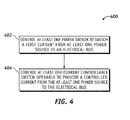
- FIG. 4 is an illustration of an exemplary flowchart showing a sequential shunt regulation process 400 according to an embodiment of the disclosure.
- the various tasks performed in connection with the process 400 may be performed mechanically, by software, hardware, firmware, or any combination thereof. It should be appreciated that process 400 may include any number of additional or alternative tasks, the tasks shown in Figure 4 need not be performed in the illustrated order, and the process 400 may be incorporated into a more comprehensive procedure or process having additional functionality not described in detail herein.
- process 400 may refer to elements mentioned above in connection with Figures 1 and 3 .
- portions of the process 400 may be performed by different elements of the systems 100 and 300 such as: the controller 102, the electrical bus 104, the PWM controlled switches 1-3, the power switches (PWR switch 1-8), the coupling lines (SA1-SA11), etc.
- the process 400 may have functions, material, and structures that are similar to the embodiments shown in Figures 1 and 3 . Therefore common features, functions, and elements may not be redundantly described here.
- Process 400 may begin by controlling at least one power switch such as at least one of the PWR switches 1-8 to switch a first current from at least one of the power sources 108 to the electrical bus 104 (task 402).
- at least one power switch such as at least one of the PWR switches 1-8 to switch a first current from at least one of the power sources 108 to the electrical bus 104 (task 402).
- Process 400 may continue by controlling at least one current controllable switch such as the PWM controlled switches 1-3 operable to provide a controlled current from the at least one of the power sources 108 to the electrical bus 104 (task 404).
- at least one current controllable switch such as the PWM controlled switches 1-3 operable to provide a controlled current from the at least one of the power sources 108 to the electrical bus 104 (task 404).
- FIG. 5 is an illustration of an exemplary flowchart showing an electrical system regulation process 500 using a sequential shunt regulator with analog fill control according to an embodiment of the disclosure.
- the various tasks performed in connection with process 500 may be performed mechanically, by software, hardware, firmware, or any combination thereof. It should be appreciated that process 500 may include any number of additional or alternative tasks, the tasks shown in Figure 5 need not be performed in the illustrated order, and the process 500 may be incorporated into a more comprehensive procedure or process having additional functionality not described in detail herein.
- process 500 may refer to elements mentioned above in connection with Figures 1 and 3 .
- portions of the process 500 may be performed by different elements of the system 100 and 300 such as: the controller 102, the electrical bus 104, the PWM controlled switches 1-3, the plurality of power switches (PWR switch 1-8), the plurality of coupling lines (SA1-SA11), etc.
- the process 500 may have functions, material, and structures that are similar to the embodiments shown in Figures 1 and 3 . Therefore common features, functions, and elements may not be redundantly described here.
- Process 500 may begin by receiving a plurality of currents from a plurality of current sources such as the power sources 108 (task 502).
- Process 500 may continue by switching a first subset of the currents in discrete amounts to provide a first current such as the combined PWR current I PWR to the electrical bus 104 (task 504).
- the first subset of currents may comprise, for example but without limitation, currents provided by a first percentage of the power sources 108 (e.g., a solar panel or a solar array string) that are sequentially coupled via respective coupling lines SA1-SA8 to the electrical bus 104 as a function of the load current of the load 122.
- the first subset may comprise currents from a first and a second solar array string each having 10A current and coupled to the electrical bus 104 via the SA1 and SA2 coupling lines respectively.
- a 0 indicates a switch providing current to the electrical bus 104
- a 1 indicates a switch not providing current to the electrical bus 104.
- 0011111 indicates PWR switches 1-2 are providing current to the electrical bus 104
- PWR switches 3-8 are not providing current to the electrical bus 104
- Process 500 may continue by providing a second subset of the currents in analog amounts to provide a second current (e.g., the combined PWM current I PWM ) to the electrical bus 104 (task 506).
- the second subset may comprise, for example but without limitation, currents provided by a second percentage of the power sources 108 that are simultaneously coupled via respective SA9-SA11 coupling lines to the electrical bus 104 as a function of the load current.
- the second subset may comprise currents from a first, a second and a third solar array string each having 10A current and coupled to the electrical bus 104 via the SA9, SA10, and SA11 coupling lines respectively.
- the PWR switches 1-2 coupled to the first percentage of the power sources 108 deliver the first current in discrete amounts comprising 20A to the electrical bus 104.
- the PWM controlled switches 1-3 coupled to the second percentage of the power sources 108 deliver the second current in analog amounts comprising 15A to the electrical bus 104.
- a total current such as the bus current I BUS delivered to the electrical bus 104 is 35A.
- the controller 102 would increase a duty cycle of the PWM controlled switches 1-3 to increase the second current to 19A. Similarly, if the load current is increased to 41A, then the controller 102 would command an additional power switch from the PWR switches 1-8 to release an additional power source from the power sources 108 to increase the first current to 30A, and the controller 102 would decrease a duty cycle of the PWM controlled switches 1-3 to decrease the second current to 11 A.
- Process 500 may continue by the controller 102 controlling the discrete amounts and the analog amounts to substantially match the first current plus the second current to the load 122 on the electrical bus 104 (task 508).
- the controller 102 controls the PWM controlled switches 1-3 to increase a duty cycle thereof to supply 19A of the analog amounts to the electrical bus 104.
- the controller 102 controls the PWR switches 1-8 to release an additional power source from the power sources 108 providing the first current comprising 30A of the discrete amounts from three power sources via respective coupling lines SA1-SA8 thereof to the electrical bus 104.
- the second current delivered by the PWM controlled switches 1-3 from coupling lines SA9-SA11 decreases to 11A of the analog amounts accordingly.
- Process 500 may continue by the controller 102 controlling a controllable voltage converter such as one of the PWM controlled switches 1-3 to provide the second subset of the currents in analog amounts (task 510).
- a controllable voltage converter such as one of the PWM controlled switches 1-3 to provide the second subset of the currents in analog amounts (task 510).
- the voltage converter may comprise, for example but without limitation, a controllable voltage converter, a controllable boost converter, a controllable buck converter, at least one controllable voltage converter comprising at least one controllable boost converter, and the like.
- Process 500 may continue by the controller 102 monitoring the status signal 112 (PWR SW status signal 112) of the power switches (PWR switch 1-8) (task 512).
- Process 500 may continue by the controller 102 generating the analog PWM error signal 118 based on the status signal 112 (PWR SW status signal 112) (task 514).
- Process 500 may continue by the controller 102 controlling the analog amounts based on the analog PWM error signal 118 (task 516).
- the analog PWM error signal 118 may be proportional to a current delivered from the power sources 108 (current sources) to the electrical bus 104.
- the PWR SW status signal 112 may be subtracted from the voltage error signal 202 to produce the analog PWM error signal 118.
- Process 500 may continue by the controller 102 shunting at least one of the currents to the ground 120 by at least one of the power switches (PWR switch 1-8) (task 518).
- embodiments of the disclosure provide voltage regulation for a system of power sources such as the power sources 108 switched to a load such as the load 122 on the electrical bus 104.
- analog PWM error signal is proportional to a current delivered from the current sources to the electrical bus.
- An embodiment further comprising shunting at least one of the currents to a ground using at least one of the power switches.
Landscapes
- Engineering & Computer Science (AREA)
- Power Engineering (AREA)
- Dc-Dc Converters (AREA)
- Remote Monitoring And Control Of Power-Distribution Networks (AREA)
- Direct Current Feeding And Distribution (AREA)
- Control Of Voltage And Current In General (AREA)
Abstract
Description
- Embodiments of the present disclosure relate generally to electrical systems. More particularly, embodiments of the present disclosure relate to regulated electrical systems.
- Some electrical power systems comprise a plurality of power sources working in combination to provide power. For example, in spacecraft and satellite applications, power from a bank of solar panels must be matched to a load or shunted to ground. As the load changes, an amount of power shunted to ground may change.
- A Pulse Width Modulation (PWM) controlled sequential shunt regulator switch system and method is disclosed. A power switch is controlled to switch a first current from a power source to an electrical bus. Further, a current controllable switch provides a controlled current from the power source to the electrical bus.
- In an embodiment, a sequential shunt regulator comprises a power switch operable to switch a current from a power source to an electrical bus. Further, a current controllable switch is operable to provide a controlled current from the power source to the electrical bus, and a controller is operable to control the power switch and the current controllable switch.
- In another embodiment, a sequential shunt regulation method controls a power switch to switch a first current from a power source to an electrical bus. The method further controls a current controllable switch operable to provide a controlled current from the power source to the electrical bus.
- In yet another embodiment, a method for regulating an electrical system using a sequential shunt regulator with analog fill control receives currents from one or more current sources. The method further switches a first subset of the currents in discrete amounts to provide a first current to an electrical bus, and provides a second subset of the currents in analog amounts to provide a second current to the electrical bus. The method also controls the discrete amounts and the analog amounts to substantially match the first current plus the second current to a load on the electrical bus.
- This summary is provided to introduce a selection of concepts in a simplified form that are further described below in the detailed description. This summary is not intended to identify key features or essential features of the claimed subject matter, nor is it intended to be used as an aid in determining the scope of the claimed subject matter.
- A more complete understanding of embodiments of the present disclosure may be derived by referring to the detailed description and claims when considered in conjunction with the following figures, wherein like reference numbers refer to similar elements throughout the figures. The figures are provided to facilitate understanding of the disclosure without limiting the breadth, scope, scale, or applicability of the disclosure. The drawings are not necessarily made to scale.
-
Figure 1 is an illustration of an exemplary PWM controlled sequential shunt regulator showing a power switch bank and a controller according to an embodiment of the disclosure. -
Figure 2 is an illustration of an exemplary graph showing operation of the power switch bank and the controller ofFigure 1 according to an embodiment of the disclosure. -
Figure 3 is an illustration of an exemplary functional block diagram of the controller ofFigure 1 according to an embodiment of the disclosure. -
Figure 4 is an illustration of an exemplary flowchart showing a PWM controlled sequential shunt regulation process according to an embodiment of the disclosure. -
Figure 5 is an illustration of an exemplary flowchart showing an electrical system regulation process using a PWM controlled sequential shunt regulator with analog fill control according to an embodiment of the disclosure. - The following detailed description is exemplary in nature and is not intended to limit the disclosure or the application and uses of the embodiments of the disclosure. Descriptions of specific devices, techniques, and applications are provided only as examples. Modifications to the examples described herein will be readily apparent to those of ordinary skill in the art, and the general principles defined herein may be applied to other examples and applications without departing from the spirit and scope of the disclosure. The present disclosure should be accorded scope consistent with the claims, and not limited to the examples described and shown herein.
- Embodiments of the disclosure may be described herein in terms of functional and/or logical block components and various processing steps. It should be appreciated that such block components may be realized by any number of hardware, software, and/or firmware components configured to perform the specified functions. For the sake of brevity, conventional techniques and components related to power switches, analog and digital circuit design, and other functional aspects of the systems (and the individual operating components of the systems) may not be described in detail herein. In addition, those skilled in the art will appreciate that embodiments of the present disclosure may be practiced in conjunction with a variety of hardware and software, and that the embodiments described herein are merely example embodiments of the disclosure.
- Embodiments of the disclosure are described herein in the context of a practical non-limiting application, namely, voltage regulation on a manned and unmanned spacecraft or satellite electrical bus. Embodiments of the disclosure, however, are not limited to such spacecraft or satellite applications, and the techniques described herein may also be utilized in other applications. For example but without limitation, embodiments may be applicable to manned and unmanned aircraft, ships, automobiles, buildings, trains, submarines, various voltage conversion applications and circuits , and the like.
- As would be apparent to one of ordinary skill in the art after reading this description, the following are examples and embodiments of the disclosure and are not limited to operating in accordance with these examples. Other embodiments may be utilized and structural changes may be made without departing from the scope of the exemplary embodiments of the present disclosure.
- Embodiments of the disclosure provide a circuit for a regulated bus system operating a number of power sources such as solar array strings or other power sources to deliver a current to substantially match a load current drawn by a load on the regulated bus system. A first subset of the power sources are sequentially coupled (e.g., all current or no current) to an electrical bus as a function of the load current. A second subset of the power sources are controlled in an analog fashion to supply an analog current providing a difference between the sequentially coupled power sources capability and the load current. In this manner, a current provided by the power sources is substantially matched to the load current.
-
Figure 1 is an illustration of an exemplary PWM sequential shunt regulator (system 100) showing a power switch bank and a controller according to an embodiment of the disclosure. Thesystem 100 comprises acontroller 102, anelectrical bus 104, a power switch bank such as a plurality of power switches (PWR switch 1-8), a plurality of coupling lines (SA1-SA8) coupling the power switches (PWR switch 1-8) to a plurality ofpower sources 108, a plurality of PWM controlled switches 1-3, a plurality of coupling lines (SA9-SA11) coupling the PWM controlled switches 1-3 to the plurality ofpower sources 108, and aload 122. Although 8 PWR switches, 3 PWM controlled switches, and 11 coupling lines are used in the embodiment shown inFigure 1 , any number of switches and coupling lines suitable for operation ofsystem 100 may also be used. In this document, power sources and current sources may be used interchangeably. - The
controller 102 receives abus voltage signal 106, a PWR switch (SW) status signal 112 (status signal of power switches), and a power source telemetry (SA TM)signal 116. Thebus voltage signal 106 is compared to a busreference voltage signal 110, and a voltage error signal such as a voltage error signal 202 (Figure 2 ) comprising a difference between thebus voltage signal 106 and the busreference voltage signal 110 is computed. The busreference voltage signal 110 represents a desired voltage for theelectrical bus 104 and may be generated by, for example but without limitation, a calibrated voltage source, a controlled voltage source, a controlled voltage source set by thecontroller 102, and the like. - The
voltage error signal 202 may be an output voltage of an error amplifier (not shown) of thecontroller 102, and may be proportional to a bus current IBUS delivered to theelectrical bus 104. When thebus voltage signal 106 is lower than the busreference voltage signal 110, thevoltage error signal 202 increases. In response to an increase in thevoltage error signal 202, thecontroller 102 causes the bus current IBUS to be delivered to theload 122 at a current that is greater than or equal to the load current. When thebus voltage signal 106 is higher than the busreference voltage signal 110, thevoltage error signal 202 decreases. In response to a decrease in thevoltage error signal 202, thecontroller 102 causes the bus current IBUS to be delivered to theelectrical bus 104 at a current that is less than or equal to the load current. In this manner, the bus current IBUS is substantially matched to the load current, and thebus voltage signal 106 is substantially matched to the busreference voltage signal 110. - The
controller 102 may further compare thevoltage error signal 202 to a sequence of voltage thresholds, and direct a PWR switch control module 310 (Figure 3 ) to sequentially activate PWR switches 1-8 until the bus current IBUS delivered to theelectrical bus 104 substantially matches the load current. When thevoltage error signal 202 reaches a steady state, thevoltage error signal 202 may substantially equal a voltage that produces the bus current IBUS at a current that substantially matches the load current. Thecontroller 102 controls and drives the PWR switches 1-8 via the PWRSW drive 114. - The
controller 102 monitors the PWRSW status signal 112 of the PWR switches 1-8 and generates an analogPWM error signal 118 which is proportional to a current delivered from thepower sources 108 to theelectrical bus 104. In this manner, the PWRSW status signal 112 is subtracted from thevoltage error signal 202 to produce the analogPWM error signal 118. The analogPWM error signal 118 controls an amount of current delivered from thepower sources 108 by the PWM controlled switches 1-3 to deliver 4a current from at least one of thepower sources 108 to substantially match theload 122 on theelectrical bus 104. - Each time one of the
power sources 108 is coupled to theelectrical bus 104, or decoupled from theelectrical bus 104 and shunted to ground 120 by the PWRswitch control module 310, the analogPWM error signal 118 sent to the PWM controlled switches 1-3 may need to be re-centered. The analogPWM error signal 118 is re-centered to control the PWM controlled switches 1-3 to deliver a current required to substantially match theload 122 on theelectrical bus 104. - The
electrical bus 104 may comprise, for example but without limitation, a spacecraft power bus, a satellite power bus, a ship electrical bus, an automobile electrical bus, a power grid electrical bus, a battery bus, a manned and unmanned spacecraft bus, a manned and unmanned aircraft bus, a building bus, a train bus, a submarine bus, various voltage conversion applications and circuits, and the like. - The PWM controlled switches 1-3 are current controllable switches comprising a first PWM switch (PWM switch 1), a second PWM switch (PWM switch 2), and a third PWM switch (PWM switch 3). Each of the PWM controlled switches 1-3 is operable to provide power from the
power sources 108 to theelectrical bus 104 at a controlled current and/or a controlled voltage as explained in more detail below. The PWM controlled switches 1-3 may comprise, for example but without limitation, a controllable voltage converter, a controllable boost converter, a controllable buck converter, at least one controllable voltage converter comprising at least one controllable boost converter, and the like. - The power switches (PWR switch 1-8) are operable to couple the
power sources 108 to theelectrical bus 104 via coupling lines (SA1-SA8). At discrete levels substantially proportional to the bus current IBUS of theelectrical bus 104, comparators such as a voltage threshold module 308 (Figure 3 ) of thecontroller 102 change state to increase or decrease a number of thepower sources 108 coupled via the coupling lines SA1-SA8 to theelectrical bus 104. In this manner, the PWRSW status signal 112 changes to indicate a number of thepower sources 108 that are coupled to theelectrical bus 104. - The
power sources 108 may comprise, for example but without limitation, solar panels, solar array strings, fuels cells, batteries, generators, satellite power sources, spacecraft power sources, aircraft power sources, shipboard generators, train power sources, solar and engine powered long-duration aircraft and spacecraft (manned and unmanned) power sources, a super-heated thermal couple from a reactor, and the like. - The
load 122 may comprise, for example but without limitation, an electronic device, a motor, a heater, a power distribution system, an appliance, an additional electrical bus, and the like. Theload 122 may be coupled to thepower sources 108 via theelectrical bus 104. -
Figure 2 is an illustration of an exemplary graph (graph 200) showing operation of the power switches (PWR switch 1-8), and thecontroller 102 ofFigure 1 according to an embodiment of the disclosure. Thegraph 200 shows afirst plot 226, asecond plot 228, and athird plot 230. - The
first plot 226 shows a relationship between error voltages represented by thevoltage error signal 202 and a PWM error voltage signal 204 (analogPWM error signal 118 inFigure 1 ) as a function of a load current proportional voltage Vlcp. The load current proportional voltage Vlcp may be, for example, a voltage proportional to a load current of theload 122. The bus current IBUS comprises a total current delivered to theelectrical bus 104 from the PWR switches 1-8 and the PWM controlled switches 1-3. The load current proportional voltage Vlcp may be, for example but without limitation, a signal that is 0.1 times the bus current IBuS. Thevoltage error signal 202 is proportional to the bus current IBUS. Therefore, as shown inFigure 2 , for example, as thevoltage error signal 202 increases from 0 to 11V, the bus current I BUS increases from 0 to 110A. - The PWM
error voltage signal 204 is proportional to a combined PWM current IPWM delivered to theelectrical bus 104 by the PWM controlled switches 1-3. For example, as shown inFigure 2 , the PWMerror voltage signal 204 may be active in a range of 12V to 2V such that as the PWMerror voltage signal 204 decreases from 12V to 0V, the combined PWM current IPWM increases from 0A to 30A. - The
second plot 228 shows drive voltages 210-224 generated by respective drive lines of the PWR SW drive 114 of each of the PWR switches 1-8 as a function of the load current proportional voltage Vlcp. - The
third plot 230 shows a relationship between a combined PWR current IPWR, the combined PWM current IPWM, and the bus current IBUS as a function of the load current proportional voltage Vlcp. The combined PWR current IPWR is provided by the PWR switches 1-8 from thepowers sources 108, the combined PWM current IPWM is provided by the PWM controlled switches 1-3 from thepowers sources 108, and the bus current IBUS is a sum of the combined PWR current IPWR and the combined PWM current IPWM. - The
second plot 228 together with thefirst plot 226 and thethird plot 230 show a relationship between thevoltage error signal 202, the PWMerror voltage signal 204, and the drive voltages 210-224 of each of the PWR switches 1-8 generated by respective drive lines of the PWR SW drive 114 as a function of the load current proportional voltage Vlcp. For example, when the bus current IBUS (Figure 1 ) reaches 20A, afirst PWR switch 1 turns off as indicated by adrive voltage 210 for thefirst PWR switch 1 changing to 0V and thefirst PWR switch 1 delivers 10A to theelectrical bus 104. When thedrive voltage 210 for thefirst PWR switch 1 changes to 0V, the PWMerror voltage signal 204 is substantially immediately increased by 4V (e.g., from 4V to 8V), which corresponds to a 10A correction in the combined PWM current IPWM delivered by the PWM controlled switches 1-3. - In this example, the process of the
second plot 228repeats 8 times as the bus current IBUS increases from 20A to 90A. At 90A, all of the PWR switches 1-8 deliver the combined PWR current IPWR to theelectrical bus 104. For load currents between 90A and 110A, the PWM controlled switches 1-3 continue to deliver additional current to theelectrical bus 104 until all of the coupling lines SA1-SA8 coupled to the power sources 108 (e.g., solar array strings) are delivering full current to theelectrical bus 104. In this manner, thepower sources 108 deliver the bus current IBUS required to substantially match theload 122 on theelectrical bus 104. Each of the PWM controlled switches 1-3 thereby provides power from thepower sources 108 to theelectrical bus 104 at a controlled current and/or a controlled voltage as mentioned above. -
Figure 3 is an illustration of an exemplary functional block diagram (system 300) of thecontroller 102 ofFigure 1 according to an embodiment of the disclosure. Thesystem 300 generally comprises aprocessor module 302, amemory module 304, atelemetry module 306, avoltage threshold module 308, the PWRswitch control module 310, and a PWMswitch control module 312. These modules may be coupled to and communicate with each other via anetwork bus 314. - The
processor module 302 comprises processing logic that is configured to carry out the functions, techniques, and processing tasks associated with the operation of thesystem 300. In particular, the processing logic is configured to support thesystem 300 described herein. For example, theprocessor module 302 may receive signals such as thebus voltage signal 106, the PWRSW status signal 112, and the power source telemetry (SA TM) signal 116 from thesystem 100 and send these signals to thetelemetry module 306, and the like. - For another example, the
processor module 302 may control discrete amounts of a subset of currents as well as analog amounts of another subset of currents from thepower sources 108 to substantially match a sum of these subsets of the currents to theload 122 on theelectrical bus 104 as explained in more detail below in the context of discussion ofFigure 5 . Further, theprocessor module 302 accesses thememory module 304 such as access to the busreference voltage signal 110, voltage thresholds, and the like. - The
processor module 302 may be implemented, or realized, with a general purpose processor, a content addressable memory, a digital signal processor, an application specific integrated circuit, a field programmable gate array, any suitable programmable logic device, discrete gate or transistor logic, discrete hardware components, or any combination thereof, designed to perform the functions described herein. - In this manner, a processor may be realized as a microprocessor, a controller, a microcontroller, a state machine, or the like. A processor may also be implemented as a combination of computing devices, e.g., a combination of a digital signal processor and a microprocessor, a plurality of microprocessors, one or more microprocessors in conjunction with a digital signal processor core, or any other such configuration.
- The
memory module 304 may be a data storage area with memory formatted to support the operation of thesystem 300. Thememory module 304 is configured to store, maintain, and provide data as needed to support the functionality of thesystem 300 in the manner described below. The data may comprise, for example but without limitation, thevoltage error signal 202, the busreference voltage signal 110, voltage thresholds, and the like. In practical embodiments, thememory module 304 may comprise, for example but without limitation, a non-volatile storage device (non-volatile semiconductor memory, hard disk device, optical disk device, and the like), a random access storage device (for example, SRAM, DRAM), or any other form of storage medium known in the art. - The
memory module 304 may be coupled to theprocessor module 302 and configured to store, for example but without limitation, a database, and the like. Additionally, thememory module 304 may represent a dynamically updating database containing a table for updating the database, and the like. Thememory module 304 may also store, a computer program that is executed by theprocessor module 302, an operating system, an application program, tentative data used in executing a program, and the like. - The
memory module 304 may be coupled to theprocessor module 302 such that theprocessor module 302 can read information from and write information to thememory module 304. As an example, theprocessor module 302 andmemory module 304 may reside in respective application specific integrated circuits (ASICs). Thememory module 304 may also be integrated into theprocessor module 302. In an embodiment, thememory module 304 may comprise a cache memory for storing temporary variables or other intermediate information during execution of instructions to be executed by theprocessor module 302. - The
telemetry module 306 receives thebus voltage signal 106, the PWRswitch status signal 112, and the power source telemetry (SA TM)signal 116. Thebus voltage signal 106 is compared to the busreference voltage signal 110, and thevoltage error signal 202 comprising a difference between thebus voltage signal 106 and the busreference voltage signal 110 is computed. - The
voltage threshold module 308 compares thevoltage error signal 202 to a sequence of voltage thresholds, and directs the PWRswitch control module 310 to activate PWR switches 1-8 until thevoltage error signal 202 causes the current delivered to theelectrical bus 104 to be equal to the load current. The sequence of voltage thresholds may comprise, for example but without limitation, 2V, 3V, 4V, 5V, 6V, 7V, 8V, 9V, and the like. - The PWR
switch control module 310 controls and drives the PWR switches 1-8 via the PWR SW drive 114 (Figure 1 ). - The PWM
switch control module 312 monitors the PWRSW status signal 112 of the PWR switches 1-8 and generates the analogPWM error signal 118 which is proportional to a current delivered to theelectrical bus 104 by the PWM controlled switches 1-3. The PWRSW status signal 112 is subtracted from thevoltage error signal 202 to produce the analogPWM error signal 118 to control an amount of current delivered by the PWM controlled switches 1-3. As explained above, each time one of thepower sources 108 such as a solar array string is coupled to theelectrical bus 104 or decoupled from theelectrical bus 104 and shunted to ground 120 by the PWMswitch control module 312, the analogPWM error signal 118 coupled to the PWM controlled switches 1-3 may need to be re-centered. The analogPWM error signal 118 is re-centered to control the PWM controlled switches 1-3 to deliver extra current required to support the load 122 (Figure 1 ) on theelectrical bus 104. -
Figure 4 is an illustration of an exemplary flowchart showing a sequentialshunt regulation process 400 according to an embodiment of the disclosure. The various tasks performed in connection with theprocess 400 may be performed mechanically, by software, hardware, firmware, or any combination thereof. It should be appreciated thatprocess 400 may include any number of additional or alternative tasks, the tasks shown inFigure 4 need not be performed in the illustrated order, and theprocess 400 may be incorporated into a more comprehensive procedure or process having additional functionality not described in detail herein. - For illustrative purposes, the following description of
process 400 may refer to elements mentioned above in connection withFigures 1 and3 . In practical embodiments, portions of theprocess 400 may be performed by different elements of thesystems controller 102, theelectrical bus 104, the PWM controlled switches 1-3, the power switches (PWR switch 1-8), the coupling lines (SA1-SA11), etc. Theprocess 400 may have functions, material, and structures that are similar to the embodiments shown inFigures 1 and3 . Therefore common features, functions, and elements may not be redundantly described here. -
Process 400 may begin by controlling at least one power switch such as at least one of the PWR switches 1-8 to switch a first current from at least one of thepower sources 108 to the electrical bus 104 (task 402). -
Process 400 may continue by controlling at least one current controllable switch such as the PWM controlled switches 1-3 operable to provide a controlled current from the at least one of thepower sources 108 to the electrical bus 104 (task 404). -
Figure 5 is an illustration of an exemplary flowchart showing an electricalsystem regulation process 500 using a sequential shunt regulator with analog fill control according to an embodiment of the disclosure. The various tasks performed in connection withprocess 500 may be performed mechanically, by software, hardware, firmware, or any combination thereof. It should be appreciated thatprocess 500 may include any number of additional or alternative tasks, the tasks shown inFigure 5 need not be performed in the illustrated order, and theprocess 500 may be incorporated into a more comprehensive procedure or process having additional functionality not described in detail herein. - For illustrative purposes, the following description of
process 500 may refer to elements mentioned above in connection withFigures 1 and3 . In practical embodiments, portions of theprocess 500 may be performed by different elements of thesystem controller 102, theelectrical bus 104, the PWM controlled switches 1-3, the plurality of power switches (PWR switch 1-8), the plurality of coupling lines (SA1-SA11), etc. - The
process 500 may have functions, material, and structures that are similar to the embodiments shown inFigures 1 and3 . Therefore common features, functions, and elements may not be redundantly described here. -
Process 500 may begin by receiving a plurality of currents from a plurality of current sources such as the power sources 108 (task 502). -
Process 500 may continue by switching a first subset of the currents in discrete amounts to provide a first current such as the combined PWR current IPWR to the electrical bus 104 (task 504). The first subset of currents may comprise, for example but without limitation, currents provided by a first percentage of the power sources 108 (e.g., a solar panel or a solar array string) that are sequentially coupled via respective coupling lines SA1-SA8 to theelectrical bus 104 as a function of the load current of theload 122. For example but without limitation, the first subset may comprise currents from a first and a second solar array string each having 10A current and coupled to theelectrical bus 104 via the SA1 and SA2 coupling lines respectively. - In this example, the discrete amounts corresponding to the first current comprise 2x10A = 20A with the PWR
SW status signal 112 corresponding to 00111111 in bit notation. In the bit notation, a 0 indicates a switch providing current to theelectrical bus 104, and a 1 indicates a switch not providing current to theelectrical bus 104. Thus, 0011111 indicates PWR switches 1-2 are providing current to theelectrical bus 104, and PWR switches 3-8 are not providing current to theelectrical bus 104 -
Process 500 may continue by providing a second subset of the currents in analog amounts to provide a second current (e.g., the combined PWM current IPWM) to the electrical bus 104 (task 506). The second subset may comprise, for example but without limitation, currents provided by a second percentage of thepower sources 108 that are simultaneously coupled via respective SA9-SA11 coupling lines to theelectrical bus 104 as a function of the load current. For example but without limitation, the second subset may comprise currents from a first, a second and a third solar array string each having 10A current and coupled to theelectrical bus 104 via the SA9, SA10, and SA11 coupling lines respectively. - By operating the PWM switches at approximately 50%, the analog amounts of the second current flowing to and received at the
electrical bus 104 may comprise 3*5A=15A. In this example, the PWR switches 1-2 coupled to the first percentage of thepower sources 108 deliver the first current in discrete amounts comprising 20A to theelectrical bus 104. Also in this example, the PWM controlled switches 1-3 coupled to the second percentage of thepower sources 108 deliver the second current in analog amounts comprising 15A to theelectrical bus 104. Thus in this example, a total current such as the bus current IBUS delivered to theelectrical bus 104 is 35A. - If the load current of the
load 122 on theelectrical bus 104 is increased to 39A, thecontroller 102 would increase a duty cycle of the PWM controlled switches 1-3 to increase the second current to 19A. Similarly, if the load current is increased to 41A, then thecontroller 102 would command an additional power switch from the PWR switches 1-8 to release an additional power source from thepower sources 108 to increase the first current to 30A, and thecontroller 102 would decrease a duty cycle of the PWM controlled switches 1-3 to decrease the second current to 11 A. -
Process 500 may continue by thecontroller 102 controlling the discrete amounts and the analog amounts to substantially match the first current plus the second current to theload 122 on the electrical bus 104 (task 508). For example, as mentioned above, if the load current of theload 122 increases from 35A to 39A, thecontroller 102 controls the PWM controlled switches 1-3 to increase a duty cycle thereof to supply 19A of the analog amounts to theelectrical bus 104. In this manner, the bus current IBUS comprises 19A of the analog amounts plus 20A of the discrete amounts supplied from two power sources (2x10A = 20A), which substantially matches a load current of 39A. - From the above example, if the load current increases from 35A to 41 A, then the
controller 102 controls the PWR switches 1-8 to release an additional power source from thepower sources 108 providing the first current comprising 30A of the discrete amounts from three power sources via respective coupling lines SA1-SA8 thereof to theelectrical bus 104. Thus in the above example, the second current delivered by the PWM controlled switches 1-3 from coupling lines SA9-SA11 decreases to 11A of the analog amounts accordingly. In this manner, for this example, the bus current IBUS comprises the first current comprising 30A of the discrete amounts supplied from three power sources (3x10A = 30A) plus the second current comprising 11A of the analog amounts, which substantially matches the load current of 41 A. -
Process 500 may continue by thecontroller 102 controlling a controllable voltage converter such as one of the PWM controlled switches 1-3 to provide the second subset of the currents in analog amounts (task 510). - The voltage converter may comprise, for example but without limitation, a controllable voltage converter, a controllable boost converter, a controllable buck converter, at least one controllable voltage converter comprising at least one controllable boost converter, and the like.
-
Process 500 may continue by thecontroller 102 monitoring the status signal 112 (PWR SW status signal 112) of the power switches (PWR switch 1-8) (task 512). -
Process 500 may continue by thecontroller 102 generating the analogPWM error signal 118 based on the status signal 112 (PWR SW status signal 112) (task 514). -
Process 500 may continue by thecontroller 102 controlling the analog amounts based on the analog PWM error signal 118 (task 516). The analogPWM error signal 118 may be proportional to a current delivered from the power sources 108 (current sources) to theelectrical bus 104. As explained above, the PWRSW status signal 112 may be subtracted from thevoltage error signal 202 to produce the analogPWM error signal 118. -
Process 500 may continue by thecontroller 102 shunting at least one of the currents to theground 120 by at least one of the power switches (PWR switch 1-8) (task 518). - In this way, embodiments of the disclosure provide voltage regulation for a system of power sources such as the
power sources 108 switched to a load such as theload 122 on theelectrical bus 104. - The above description refers to elements or nodes or features being "connected" or "coupled" together. As used herein, unless expressly stated otherwise, "connected" means that one element/node/feature is directly joined to (or directly communicates with) another element/node/feature, and not necessarily mechanically. Likewise, unless expressly stated otherwise, "coupled" means that one element/node/feature is directly or indirectly joined to (or directly or indirectly communicates with) another element/node/feature, and not necessarily mechanically. Thus, although
Figures 1 and3 depict example arrangements of elements, additional intervening elements, devices, features, or components may be present in an embodiment of the disclosure. - Terms and phrases used in this document, and variations thereof, unless otherwise expressly stated, should be construed as open ended as opposed to limiting. As examples of the foregoing: the term "including" should be read as mean "including, without limitation" or the like; the term "example" is used to provide exemplary instances of the item in discussion, not an exhaustive or limiting list thereof; and adjectives such as "conventional," "traditional," "normal," "standard," "known" and terms of similar meaning should not be construed as limiting the item described to a given time period or to an item available as of a given time, but instead should be read to encompass conventional, traditional, normal, or standard technologies that may be available or known now or at any time in the future.
- Likewise, a group of items linked with the conjunction "and" should not be read as requiring that each and every one of those items be present in the grouping, but rather should be read as "and/or" unless expressly stated otherwise. Similarly, a group of items linked with the conjunction "or" should not be read as requiring mutual exclusivity among that group, but rather should also be read as "and/or" unless expressly stated otherwise. Furthermore, although items, elements or components of the disclosure may be described or claimed in the singular, the plural is contemplated to be within the scope thereof unless limitation to the singular is explicitly stated. The presence of broadening words and phrases such as "one or more," "at least," "but not limited to" or other like phrases in some instances shall not be read to mean that the narrower case is intended or required in instances where such broadening phrases may be absent.
- Other embodiments are possible namely, an embodiment wherein the voltage converter comprises a controllable boost converter. An embodiment, further comprising:
- monitoring a status signal of a plurality of power switches;
- generating an analog PWM error signal based on the status signal; and controlling the analog amounts based on the analog PWM error signal.
- An embodiment wherein the analog PWM error signal is proportional to a current delivered from the current sources to the electrical bus.
- An embodiment wherein the status signal is subtracted from a voltage error signal to produce the analog PWM error signal.
- An embodiment , further comprising shunting at least one of the currents to a ground using at least one of the power switches.
Claims (11)
- A sequential shunt regulator comprising:at least one power switch operable to switch a current from at least one power source to an electrical bus;at least one current controllable switch operable to provide a controlled current from the at least one power source to the electrical bus; anda controller operable to control the at least one power switch and the at least one current controllable switch.
- The sequential shunt regulator according to claim 1, wherein the at least one power switch is further operable to shunt the current to a ground.
- The sequential shunt regulator according to claim 1, wherein the at least one current controllable switch comprises at least one controllable voltage converter.
- The sequential shunt regulator according to claim 3, wherein the at least one controllable voltage converter comprises at least one controllable boost converter.
- The sequential shunt regulator according to claim 1, further comprising the at least one power source, and the electrical bus.
- The sequential shunt regulator according to claim 1, wherein the at least one power source comprises at least one solar panel.
- A sequential shunt regulation method, the method comprising:controlling at least one power switch to switch a first current from at least one power source to an electrical bus; andcontrolling at least one current controllable switch operable to provide a controlled current from the at least one power source to the electrical bus.
- The method according to claim 7, further comprising:receiving a plurality of currents from a plurality of current sources;switching a first subset of the currents in discrete amounts to provide the first current to the electrical bus;providing a second subset of the currents in analog amounts to provide a second current to the electrical bus; andcontrolling the discrete amounts and the analog amounts to substantially match a sum of the first current and the second current to a load on the electrical bus.
- The method according to claim 7, wherein the at least one power switch is further operable to switch the first current to a ground, wherein the at least one current controllable switch comprises at least one controllable voltage converter and wherein the at least one controllable voltage converter comprises at least one controllable boost converter.
- A method for regulating an electrical system using a sequential shunt regulator with analog fill control, the method comprising:receiving a plurality of currents from a plurality of current sources;switching a first subset of the currents in discrete amounts to provide a first current to an electrical bus;providing a second subset of the currents in analog amounts to provide a second current to the electrical bus; andcontrolling the discrete amounts and the analog amounts to substantially match the first current plus the second current to a load on the electrical bus.
- The method according to claim 10, wherein the current sources comprise at least one solar panel; and
further comprising controlling a voltage converter to provide the second subset of the currents in analog amounts.
Applications Claiming Priority (1)
| Application Number | Priority Date | Filing Date | Title |
|---|---|---|---|
| US13/072,769 US8587152B2 (en) | 2011-03-27 | 2011-03-27 | Sequential shunt regulator with analog fill control |
Publications (2)
| Publication Number | Publication Date |
|---|---|
| EP2506412A1 true EP2506412A1 (en) | 2012-10-03 |
| EP2506412B1 EP2506412B1 (en) | 2015-10-21 |
Family
ID=46000731
Family Applications (1)
| Application Number | Title | Priority Date | Filing Date |
|---|---|---|---|
| EP12161566.0A Active EP2506412B1 (en) | 2011-03-27 | 2012-03-27 | Sequential shunt regulator with analog fill control |
Country Status (4)
| Country | Link |
|---|---|
| US (1) | US8587152B2 (en) |
| EP (1) | EP2506412B1 (en) |
| JP (1) | JP5941722B2 (en) |
| CN (1) | CN102749951B (en) |
Families Citing this family (4)
| Publication number | Priority date | Publication date | Assignee | Title |
|---|---|---|---|---|
| EP2705414A2 (en) * | 2011-05-06 | 2014-03-12 | SunEdison LLC | Solar power systems including control hubs |
| KR102049642B1 (en) * | 2017-11-24 | 2019-11-27 | (주)두산 모빌리티 이노베이션 | Fuel cell powerpack for drone, and state information monitoring method thereof |
| CN111457927B (en) * | 2020-04-26 | 2021-03-05 | 北京工商大学 | Multi-objective path planning method for unmanned cruise ship under dynamic obstacles |
| CN112650377B (en) * | 2020-12-22 | 2022-09-02 | 海光信息技术股份有限公司 | I2C bus pull-up power supply method, circuit and chip |
Citations (5)
| Publication number | Priority date | Publication date | Assignee | Title |
|---|---|---|---|---|
| US3696286A (en) * | 1970-08-06 | 1972-10-03 | North American Rockwell | System for detecting and utilizing the maximum available power from solar cells |
| US3896368A (en) * | 1972-10-20 | 1975-07-22 | Acec | Voltage regulating device |
| US4186336A (en) * | 1977-03-31 | 1980-01-29 | Organisation Europeenne De Recherches Spatiales | Limit cycling regulator apparatus for plural parallel power sources |
| US6979986B2 (en) * | 2003-06-11 | 2005-12-27 | Alcatel | Switch shunt regulator and power supply arrangement using same for spacecraft applications |
| EP2267572A1 (en) * | 2009-06-16 | 2010-12-29 | Agence Spatiale Européenne | Solar array regulator based on step-up and down conversion and solar power system comprising the same |
Family Cites Families (9)
| Publication number | Priority date | Publication date | Assignee | Title |
|---|---|---|---|---|
| US3930864A (en) | 1974-04-15 | 1976-01-06 | Eastman Kodak Company | Auxiliary mordant layer for excess dye formed in integral color transfer assemblage |
| AU1336700A (en) * | 1998-10-30 | 2000-05-22 | Volterra Semiconductor Corporation | Method and apparatus for digital voltage regulation |
| JP3934050B2 (en) * | 2000-10-10 | 2007-06-20 | プリマリオン, インコーポレイテッド | System and method for highly phased power regulation |
| US8866465B2 (en) * | 2005-08-29 | 2014-10-21 | The Aerospace Corporation | Nanosatellite photovoltaic regulator |
| KR101129388B1 (en) * | 2007-04-30 | 2012-03-26 | 삼성전자주식회사 | Power supply device having multiple outputs |
| US7777367B2 (en) * | 2008-04-08 | 2010-08-17 | The Boeing Company | Sequential shunt solar array controller |
| CN201426083Y (en) * | 2009-05-27 | 2010-03-17 | 深圳桑达国际电子器件有限公司 | Sawtooth signal control circuit and switch power supply |
| EP2330476B1 (en) * | 2009-11-27 | 2013-07-10 | Agence Spatiale Européenne | Sequential switching shunt regulator cell with non-redundant rectifier |
| CN101867289B (en) * | 2010-05-19 | 2012-05-30 | 杭州矽力杰半导体技术有限公司 | Switch power supply with constant voltage/constant current output and control method thereof |
-
2011
- 2011-03-27 US US13/072,769 patent/US8587152B2/en active Active
-
2012
- 2012-03-26 JP JP2012070210A patent/JP5941722B2/en active Active
- 2012-03-27 EP EP12161566.0A patent/EP2506412B1/en active Active
- 2012-03-27 CN CN201210084425.6A patent/CN102749951B/en active Active
Patent Citations (5)
| Publication number | Priority date | Publication date | Assignee | Title |
|---|---|---|---|---|
| US3696286A (en) * | 1970-08-06 | 1972-10-03 | North American Rockwell | System for detecting and utilizing the maximum available power from solar cells |
| US3896368A (en) * | 1972-10-20 | 1975-07-22 | Acec | Voltage regulating device |
| US4186336A (en) * | 1977-03-31 | 1980-01-29 | Organisation Europeenne De Recherches Spatiales | Limit cycling regulator apparatus for plural parallel power sources |
| US6979986B2 (en) * | 2003-06-11 | 2005-12-27 | Alcatel | Switch shunt regulator and power supply arrangement using same for spacecraft applications |
| EP2267572A1 (en) * | 2009-06-16 | 2010-12-29 | Agence Spatiale Européenne | Solar array regulator based on step-up and down conversion and solar power system comprising the same |
Also Published As
| Publication number | Publication date |
|---|---|
| EP2506412B1 (en) | 2015-10-21 |
| US20120242154A1 (en) | 2012-09-27 |
| JP2012205501A (en) | 2012-10-22 |
| US8587152B2 (en) | 2013-11-19 |
| CN102749951B (en) | 2015-12-09 |
| JP5941722B2 (en) | 2016-06-29 |
| CN102749951A (en) | 2012-10-24 |
Similar Documents
| Publication | Publication Date | Title |
|---|---|---|
| US9531190B2 (en) | Bi-directional converter voltage controlled current source for voltage regulation | |
| Iovine et al. | Nonlinear control of a DC microgrid for the integration of photovoltaic panels | |
| Sachs et al. | Multi-objective three stage design optimization for island microgrids | |
| CN102804096B (en) | Boost and Buck Conversion Based Solar Array Regulator and Solar Cell Power System Incorporating the Regulator | |
| Azizi et al. | Autonomous and decentralized load sharing and energy management approach for DC microgrids | |
| Wang et al. | An SI-MISO boost converter with deadbeat-based control for electric vehicle applications | |
| Li et al. | A dual-window DC bus interacting method for DC microgrids hierarchical control scheme | |
| JP6198034B2 (en) | Power control apparatus, power control method, program, and energy management system | |
| US20080100143A1 (en) | Power management system with charger/boost controller | |
| US8587152B2 (en) | Sequential shunt regulator with analog fill control | |
| Mourra et al. | Buck boost regulator (B 2 R) for spacecraft solar array power conversion | |
| Basantes et al. | Power management of an off-grid photovoltaic system using a linear algebra based control | |
| Vázquez et al. | A Different Three‐Port DC/DC Converter for Standalone PV System | |
| US9537391B2 (en) | Voltage regulation of a DC/DC converter | |
| Candan et al. | A distributed bi-directional hysteresis control algorithm for server-to-virtual bus differential power processing | |
| Li et al. | A module-based hierarchical microgrid with a bottom-up building architecture for rural electrification | |
| Zhang et al. | Methods to enhance the energy supply of photovoltaic system for solar-powered unmanned aerial vehicle | |
| Venkateswaran et al. | A compact dual-output Boost-SEPIC converter with digital predictive current control for automotive accessory power applications | |
| Yang et al. | An analog-device-based five-domain control method and distributed system configuration for high-power spacecraft power systems | |
| Rajalakshmi et al. | Analysis of electrical power system (eps) dc-dc converter topologies for efficient cubesat load management | |
| Zumel et al. | Digital Control for a Modular System of DC/DC Converters for Primary Distribution System | |
| Elmayah et al. | Design and implementation of power distribution module of low earth orbit small satellite | |
| Sharma | Mitigation of Power Oscillations in DC Microgrid Using Model Predictive Control | |
| Chen et al. | Design and Implementation of Electrical Power System for LilacSat-3 with Digital Energy Management | |
| Challoob et al. | Flatness-Based Energy Management Strategy for Electric Vehicles with Photovoltaic Systems and Energy Storage Units |
Legal Events
| Date | Code | Title | Description |
|---|---|---|---|
| PUAI | Public reference made under article 153(3) epc to a published international application that has entered the european phase |
Free format text: ORIGINAL CODE: 0009012 |
|
| 17P | Request for examination filed |
Effective date: 20120327 |
|
| AK | Designated contracting states |
Kind code of ref document: A1 Designated state(s): AL AT BE BG CH CY CZ DE DK EE ES FI FR GB GR HR HU IE IS IT LI LT LU LV MC MK MT NL NO PL PT RO RS SE SI SK SM TR |
|
| AX | Request for extension of the european patent |
Extension state: BA ME |
|
| GRAP | Despatch of communication of intention to grant a patent |
Free format text: ORIGINAL CODE: EPIDOSNIGR1 |
|
| INTG | Intention to grant announced |
Effective date: 20150629 |
|
| RIN1 | Information on inventor provided before grant (corrected) |
Inventor name: MARTINELLI, ROBERT MATTHEW |
|
| GRAS | Grant fee paid |
Free format text: ORIGINAL CODE: EPIDOSNIGR3 |
|
| GRAA | (expected) grant |
Free format text: ORIGINAL CODE: 0009210 |
|
| AK | Designated contracting states |
Kind code of ref document: B1 Designated state(s): AL AT BE BG CH CY CZ DE DK EE ES FI FR GB GR HR HU IE IS IT LI LT LU LV MC MK MT NL NO PL PT RO RS SE SI SK SM TR |
|
| REG | Reference to a national code |
Ref country code: GB Ref legal event code: FG4D Ref country code: NL Ref legal event code: MP Effective date: 20151021 |
|
| REG | Reference to a national code |
Ref country code: CH Ref legal event code: EP |
|
| REG | Reference to a national code |
Ref country code: AT Ref legal event code: REF Ref document number: 757160 Country of ref document: AT Kind code of ref document: T Effective date: 20151115 |
|
| REG | Reference to a national code |
Ref country code: IE Ref legal event code: FG4D |
|
| REG | Reference to a national code |
Ref country code: DE Ref legal event code: R096 Ref document number: 602012011714 Country of ref document: DE |
|
| REG | Reference to a national code |
Ref country code: LT Ref legal event code: MG4D |
|
| REG | Reference to a national code |
Ref country code: AT Ref legal event code: MK05 Ref document number: 757160 Country of ref document: AT Kind code of ref document: T Effective date: 20151021 |
|
| REG | Reference to a national code |
Ref country code: FR Ref legal event code: PLFP Year of fee payment: 5 |
|
| PG25 | Lapsed in a contracting state [announced via postgrant information from national office to epo] |
Ref country code: IS Free format text: LAPSE BECAUSE OF FAILURE TO SUBMIT A TRANSLATION OF THE DESCRIPTION OR TO PAY THE FEE WITHIN THE PRESCRIBED TIME-LIMIT Effective date: 20160221 Ref country code: LT Free format text: LAPSE BECAUSE OF FAILURE TO SUBMIT A TRANSLATION OF THE DESCRIPTION OR TO PAY THE FEE WITHIN THE PRESCRIBED TIME-LIMIT Effective date: 20151021 Ref country code: NL Free format text: LAPSE BECAUSE OF FAILURE TO SUBMIT A TRANSLATION OF THE DESCRIPTION OR TO PAY THE FEE WITHIN THE PRESCRIBED TIME-LIMIT Effective date: 20151021 Ref country code: NO Free format text: LAPSE BECAUSE OF FAILURE TO SUBMIT A TRANSLATION OF THE DESCRIPTION OR TO PAY THE FEE WITHIN THE PRESCRIBED TIME-LIMIT Effective date: 20160121 Ref country code: ES Free format text: LAPSE BECAUSE OF FAILURE TO SUBMIT A TRANSLATION OF THE DESCRIPTION OR TO PAY THE FEE WITHIN THE PRESCRIBED TIME-LIMIT Effective date: 20151021 Ref country code: IT Free format text: LAPSE BECAUSE OF FAILURE TO SUBMIT A TRANSLATION OF THE DESCRIPTION OR TO PAY THE FEE WITHIN THE PRESCRIBED TIME-LIMIT Effective date: 20151021 Ref country code: HR Free format text: LAPSE BECAUSE OF FAILURE TO SUBMIT A TRANSLATION OF THE DESCRIPTION OR TO PAY THE FEE WITHIN THE PRESCRIBED TIME-LIMIT Effective date: 20151021 |
|
| PG25 | Lapsed in a contracting state [announced via postgrant information from national office to epo] |
Ref country code: GR Free format text: LAPSE BECAUSE OF FAILURE TO SUBMIT A TRANSLATION OF THE DESCRIPTION OR TO PAY THE FEE WITHIN THE PRESCRIBED TIME-LIMIT Effective date: 20160122 Ref country code: AT Free format text: LAPSE BECAUSE OF FAILURE TO SUBMIT A TRANSLATION OF THE DESCRIPTION OR TO PAY THE FEE WITHIN THE PRESCRIBED TIME-LIMIT Effective date: 20151021 Ref country code: FI Free format text: LAPSE BECAUSE OF FAILURE TO SUBMIT A TRANSLATION OF THE DESCRIPTION OR TO PAY THE FEE WITHIN THE PRESCRIBED TIME-LIMIT Effective date: 20151021 Ref country code: LV Free format text: LAPSE BECAUSE OF FAILURE TO SUBMIT A TRANSLATION OF THE DESCRIPTION OR TO PAY THE FEE WITHIN THE PRESCRIBED TIME-LIMIT Effective date: 20151021 Ref country code: SE Free format text: LAPSE BECAUSE OF FAILURE TO SUBMIT A TRANSLATION OF THE DESCRIPTION OR TO PAY THE FEE WITHIN THE PRESCRIBED TIME-LIMIT Effective date: 20151021 Ref country code: PL Free format text: LAPSE BECAUSE OF FAILURE TO SUBMIT A TRANSLATION OF THE DESCRIPTION OR TO PAY THE FEE WITHIN THE PRESCRIBED TIME-LIMIT Effective date: 20151021 Ref country code: PT Free format text: LAPSE BECAUSE OF FAILURE TO SUBMIT A TRANSLATION OF THE DESCRIPTION OR TO PAY THE FEE WITHIN THE PRESCRIBED TIME-LIMIT Effective date: 20160222 Ref country code: RS Free format text: LAPSE BECAUSE OF FAILURE TO SUBMIT A TRANSLATION OF THE DESCRIPTION OR TO PAY THE FEE WITHIN THE PRESCRIBED TIME-LIMIT Effective date: 20151021 |
|
| REG | Reference to a national code |
Ref country code: DE Ref legal event code: R097 Ref document number: 602012011714 Country of ref document: DE |
|
| PG25 | Lapsed in a contracting state [announced via postgrant information from national office to epo] |
Ref country code: CZ Free format text: LAPSE BECAUSE OF FAILURE TO SUBMIT A TRANSLATION OF THE DESCRIPTION OR TO PAY THE FEE WITHIN THE PRESCRIBED TIME-LIMIT Effective date: 20151021 |
|
| PLBE | No opposition filed within time limit |
Free format text: ORIGINAL CODE: 0009261 |
|
| STAA | Information on the status of an ep patent application or granted ep patent |
Free format text: STATUS: NO OPPOSITION FILED WITHIN TIME LIMIT |
|
| PG25 | Lapsed in a contracting state [announced via postgrant information from national office to epo] |
Ref country code: EE Free format text: LAPSE BECAUSE OF FAILURE TO SUBMIT A TRANSLATION OF THE DESCRIPTION OR TO PAY THE FEE WITHIN THE PRESCRIBED TIME-LIMIT Effective date: 20151021 Ref country code: DK Free format text: LAPSE BECAUSE OF FAILURE TO SUBMIT A TRANSLATION OF THE DESCRIPTION OR TO PAY THE FEE WITHIN THE PRESCRIBED TIME-LIMIT Effective date: 20151021 Ref country code: SM Free format text: LAPSE BECAUSE OF FAILURE TO SUBMIT A TRANSLATION OF THE DESCRIPTION OR TO PAY THE FEE WITHIN THE PRESCRIBED TIME-LIMIT Effective date: 20151021 Ref country code: BE Free format text: LAPSE BECAUSE OF NON-PAYMENT OF DUE FEES Effective date: 20160331 Ref country code: RO Free format text: LAPSE BECAUSE OF FAILURE TO SUBMIT A TRANSLATION OF THE DESCRIPTION OR TO PAY THE FEE WITHIN THE PRESCRIBED TIME-LIMIT Effective date: 20151021 Ref country code: SK Free format text: LAPSE BECAUSE OF FAILURE TO SUBMIT A TRANSLATION OF THE DESCRIPTION OR TO PAY THE FEE WITHIN THE PRESCRIBED TIME-LIMIT Effective date: 20151021 |
|
| 26N | No opposition filed |
Effective date: 20160722 |
|
| PG25 | Lapsed in a contracting state [announced via postgrant information from national office to epo] |
Ref country code: LU Free format text: LAPSE BECAUSE OF FAILURE TO SUBMIT A TRANSLATION OF THE DESCRIPTION OR TO PAY THE FEE WITHIN THE PRESCRIBED TIME-LIMIT Effective date: 20160327 Ref country code: MC Free format text: LAPSE BECAUSE OF FAILURE TO SUBMIT A TRANSLATION OF THE DESCRIPTION OR TO PAY THE FEE WITHIN THE PRESCRIBED TIME-LIMIT Effective date: 20151021 |
|
| REG | Reference to a national code |
Ref country code: CH Ref legal event code: PL |
|
| PG25 | Lapsed in a contracting state [announced via postgrant information from national office to epo] |
Ref country code: SI Free format text: LAPSE BECAUSE OF FAILURE TO SUBMIT A TRANSLATION OF THE DESCRIPTION OR TO PAY THE FEE WITHIN THE PRESCRIBED TIME-LIMIT Effective date: 20151021 |
|
| REG | Reference to a national code |
Ref country code: IE Ref legal event code: MM4A |
|
| PG25 | Lapsed in a contracting state [announced via postgrant information from national office to epo] |
Ref country code: BE Free format text: LAPSE BECAUSE OF FAILURE TO SUBMIT A TRANSLATION OF THE DESCRIPTION OR TO PAY THE FEE WITHIN THE PRESCRIBED TIME-LIMIT Effective date: 20151021 |
|
| PG25 | Lapsed in a contracting state [announced via postgrant information from national office to epo] |
Ref country code: LI Free format text: LAPSE BECAUSE OF NON-PAYMENT OF DUE FEES Effective date: 20160331 Ref country code: IE Free format text: LAPSE BECAUSE OF NON-PAYMENT OF DUE FEES Effective date: 20160327 Ref country code: CH Free format text: LAPSE BECAUSE OF NON-PAYMENT OF DUE FEES Effective date: 20160331 |
|
| REG | Reference to a national code |
Ref country code: FR Ref legal event code: PLFP Year of fee payment: 6 |
|
| PG25 | Lapsed in a contracting state [announced via postgrant information from national office to epo] |
Ref country code: MT Free format text: LAPSE BECAUSE OF FAILURE TO SUBMIT A TRANSLATION OF THE DESCRIPTION OR TO PAY THE FEE WITHIN THE PRESCRIBED TIME-LIMIT Effective date: 20151021 |
|
| REG | Reference to a national code |
Ref country code: FR Ref legal event code: PLFP Year of fee payment: 7 |
|
| PG25 | Lapsed in a contracting state [announced via postgrant information from national office to epo] |
Ref country code: CY Free format text: LAPSE BECAUSE OF FAILURE TO SUBMIT A TRANSLATION OF THE DESCRIPTION OR TO PAY THE FEE WITHIN THE PRESCRIBED TIME-LIMIT Effective date: 20151021 Ref country code: HU Free format text: LAPSE BECAUSE OF FAILURE TO SUBMIT A TRANSLATION OF THE DESCRIPTION OR TO PAY THE FEE WITHIN THE PRESCRIBED TIME-LIMIT; INVALID AB INITIO Effective date: 20120327 |
|
| PG25 | Lapsed in a contracting state [announced via postgrant information from national office to epo] |
Ref country code: MK Free format text: LAPSE BECAUSE OF FAILURE TO SUBMIT A TRANSLATION OF THE DESCRIPTION OR TO PAY THE FEE WITHIN THE PRESCRIBED TIME-LIMIT Effective date: 20151021 Ref country code: TR Free format text: LAPSE BECAUSE OF FAILURE TO SUBMIT A TRANSLATION OF THE DESCRIPTION OR TO PAY THE FEE WITHIN THE PRESCRIBED TIME-LIMIT Effective date: 20151021 Ref country code: MT Free format text: LAPSE BECAUSE OF FAILURE TO SUBMIT A TRANSLATION OF THE DESCRIPTION OR TO PAY THE FEE WITHIN THE PRESCRIBED TIME-LIMIT Effective date: 20160331 |
|
| PG25 | Lapsed in a contracting state [announced via postgrant information from national office to epo] |
Ref country code: BG Free format text: LAPSE BECAUSE OF FAILURE TO SUBMIT A TRANSLATION OF THE DESCRIPTION OR TO PAY THE FEE WITHIN THE PRESCRIBED TIME-LIMIT Effective date: 20151021 |
|
| PG25 | Lapsed in a contracting state [announced via postgrant information from national office to epo] |
Ref country code: AL Free format text: LAPSE BECAUSE OF FAILURE TO SUBMIT A TRANSLATION OF THE DESCRIPTION OR TO PAY THE FEE WITHIN THE PRESCRIBED TIME-LIMIT Effective date: 20151021 |
|
| REG | Reference to a national code |
Ref country code: DE Ref legal event code: R082 Ref document number: 602012011714 Country of ref document: DE Representative=s name: KILBURN & STRODE LLP, NL |
|
| P01 | Opt-out of the competence of the unified patent court (upc) registered |
Effective date: 20230516 |
|
| PGFP | Annual fee paid to national office [announced via postgrant information from national office to epo] |
Ref country code: GB Payment date: 20260327 Year of fee payment: 15 |
|
| PGFP | Annual fee paid to national office [announced via postgrant information from national office to epo] |
Ref country code: DE Payment date: 20260327 Year of fee payment: 15 |
|
| PGFP | Annual fee paid to national office [announced via postgrant information from national office to epo] |
Ref country code: FR Payment date: 20260325 Year of fee payment: 15 |