EP2506299A1 - Semiconductor device and method of producing same - Google Patents
Semiconductor device and method of producing same Download PDFInfo
- Publication number
- EP2506299A1 EP2506299A1 EP09851664A EP09851664A EP2506299A1 EP 2506299 A1 EP2506299 A1 EP 2506299A1 EP 09851664 A EP09851664 A EP 09851664A EP 09851664 A EP09851664 A EP 09851664A EP 2506299 A1 EP2506299 A1 EP 2506299A1
- Authority
- EP
- European Patent Office
- Prior art keywords
- joining
- joined
- hole
- lid
- insulating member
- Prior art date
- Legal status (The legal status is an assumption and is not a legal conclusion. Google has not performed a legal analysis and makes no representation as to the accuracy of the status listed.)
- Withdrawn
Links
Images





Classifications
-
- H—ELECTRICITY
- H10—SEMICONDUCTOR DEVICES; ELECTRIC SOLID-STATE DEVICES NOT OTHERWISE PROVIDED FOR
- H10W—GENERIC PACKAGES, INTERCONNECTIONS, CONNECTORS OR OTHER CONSTRUCTIONAL DETAILS OF DEVICES COVERED BY CLASS H10
- H10W40/00—Arrangements for thermal protection or thermal control
- H10W40/40—Arrangements for thermal protection or thermal control involving heat exchange by flowing fluids
- H10W40/47—Arrangements for thermal protection or thermal control involving heat exchange by flowing fluids by flowing liquids, e.g. forced water cooling
-
- H—ELECTRICITY
- H10—SEMICONDUCTOR DEVICES; ELECTRIC SOLID-STATE DEVICES NOT OTHERWISE PROVIDED FOR
- H10W—GENERIC PACKAGES, INTERCONNECTIONS, CONNECTORS OR OTHER CONSTRUCTIONAL DETAILS OF DEVICES COVERED BY CLASS H10
- H10W72/00—Interconnections or connectors in packages
- H10W72/01—Manufacture or treatment
- H10W72/0198—Manufacture or treatment batch processes
-
- H—ELECTRICITY
- H10—SEMICONDUCTOR DEVICES; ELECTRIC SOLID-STATE DEVICES NOT OTHERWISE PROVIDED FOR
- H10W—GENERIC PACKAGES, INTERCONNECTIONS, CONNECTORS OR OTHER CONSTRUCTIONAL DETAILS OF DEVICES COVERED BY CLASS H10
- H10W99/00—Subject matter not provided for in other groups of this subclass
-
- H—ELECTRICITY
- H10—SEMICONDUCTOR DEVICES; ELECTRIC SOLID-STATE DEVICES NOT OTHERWISE PROVIDED FOR
- H10W—GENERIC PACKAGES, INTERCONNECTIONS, CONNECTORS OR OTHER CONSTRUCTIONAL DETAILS OF DEVICES COVERED BY CLASS H10
- H10W70/00—Package substrates; Interposers; Redistribution layers [RDL]
- H10W70/60—Insulating or insulated package substrates; Interposers; Redistribution layers
- H10W70/67—Insulating or insulated package substrates; Interposers; Redistribution layers characterised by their insulating layers or insulating parts
- H10W70/68—Shapes or dispositions thereof
- H10W70/681—Shapes or dispositions thereof comprising holes not having chips therein, e.g. for outgassing, underfilling or bond wire passage
-
- H—ELECTRICITY
- H10—SEMICONDUCTOR DEVICES; ELECTRIC SOLID-STATE DEVICES NOT OTHERWISE PROVIDED FOR
- H10W—GENERIC PACKAGES, INTERCONNECTIONS, CONNECTORS OR OTHER CONSTRUCTIONAL DETAILS OF DEVICES COVERED BY CLASS H10
- H10W72/00—Interconnections or connectors in packages
- H10W72/071—Connecting or disconnecting
- H10W72/073—Connecting or disconnecting of die-attach connectors
-
- H—ELECTRICITY
- H10—SEMICONDUCTOR DEVICES; ELECTRIC SOLID-STATE DEVICES NOT OTHERWISE PROVIDED FOR
- H10W—GENERIC PACKAGES, INTERCONNECTIONS, CONNECTORS OR OTHER CONSTRUCTIONAL DETAILS OF DEVICES COVERED BY CLASS H10
- H10W72/00—Interconnections or connectors in packages
- H10W72/071—Connecting or disconnecting
- H10W72/073—Connecting or disconnecting of die-attach connectors
- H10W72/07331—Connecting techniques
-
- H—ELECTRICITY
- H10—SEMICONDUCTOR DEVICES; ELECTRIC SOLID-STATE DEVICES NOT OTHERWISE PROVIDED FOR
- H10W—GENERIC PACKAGES, INTERCONNECTIONS, CONNECTORS OR OTHER CONSTRUCTIONAL DETAILS OF DEVICES COVERED BY CLASS H10
- H10W72/00—Interconnections or connectors in packages
- H10W72/071—Connecting or disconnecting
- H10W72/073—Connecting or disconnecting of die-attach connectors
- H10W72/07351—Connecting or disconnecting of die-attach connectors characterised by changes in properties of the die-attach connectors during connecting
- H10W72/07353—Connecting or disconnecting of die-attach connectors characterised by changes in properties of the die-attach connectors during connecting changes in shapes
-
- H—ELECTRICITY
- H10—SEMICONDUCTOR DEVICES; ELECTRIC SOLID-STATE DEVICES NOT OTHERWISE PROVIDED FOR
- H10W—GENERIC PACKAGES, INTERCONNECTIONS, CONNECTORS OR OTHER CONSTRUCTIONAL DETAILS OF DEVICES COVERED BY CLASS H10
- H10W72/00—Interconnections or connectors in packages
- H10W72/30—Die-attach connectors
- H10W72/331—Shapes of die-attach connectors
- H10W72/334—Cross-sectional shape, i.e. in side view
-
- H—ELECTRICITY
- H10—SEMICONDUCTOR DEVICES; ELECTRIC SOLID-STATE DEVICES NOT OTHERWISE PROVIDED FOR
- H10W—GENERIC PACKAGES, INTERCONNECTIONS, CONNECTORS OR OTHER CONSTRUCTIONAL DETAILS OF DEVICES COVERED BY CLASS H10
- H10W72/00—Interconnections or connectors in packages
- H10W72/30—Die-attach connectors
- H10W72/351—Materials of die-attach connectors
- H10W72/352—Materials of die-attach connectors comprising metals or metalloids, e.g. solders
-
- H—ELECTRICITY
- H10—SEMICONDUCTOR DEVICES; ELECTRIC SOLID-STATE DEVICES NOT OTHERWISE PROVIDED FOR
- H10W—GENERIC PACKAGES, INTERCONNECTIONS, CONNECTORS OR OTHER CONSTRUCTIONAL DETAILS OF DEVICES COVERED BY CLASS H10
- H10W72/00—Interconnections or connectors in packages
- H10W72/90—Bond pads, in general
- H10W72/931—Shapes of bond pads
Definitions
- the present invention relates to a semiconductor device including a joining member and a joined member joined to each other by brazing, and a method of producing the semiconductor device.
- a joining member such as an insulating member (an insulating substrate)
- a joined member such as a lid of a cooler
- a brazing material placed between the joining member and the joined member is heated to be melted.
- the melted brazing material is wetted and spread with no regularity.
- the brazing material is cooled and solidified to form a joining layer, a peripheral portion of the joining member is apt to become cold first, causing the brazing material to begin solidifying from an outer peripheral edge.
- Patent document 1 discloses a technique of releasing such air.
- a pair of electrodes to which an electronic component is to be soldered are formed with guide passages for air release. These guide passages open in a clearance located under the electronic component and in the outside of the electronic component. With this configuration, the air that occurs in the clearance under the electronic component when resin is supplied to form an insulating layer is released through open ends located in the outside of the electronic component via the guide passages.
- Patent Document 1 JP 2007-258605 A
- the present invention has been made to solve the above problems and has a purpose to provide a semiconductor device and a method of producing the semiconductor device, whereby a joining member and a joined member are joined by brazing without leaving voids in a joining layer.
- one aspect of the invention provides a semiconductor device including a joining member and a joined member to which the joining member is joined by brazing, wherein the joined member includes a joining surface to be joined to the joining member and a through hole opening in the joining surface, and a passage communicated with the through hole is provided with at least one of a joining surface of the joining member to be joined to the joined member and the joining surface of the joined member to be joined to the joining member.
- the joined member is provided with the through hole opening in the joining surface to be joined to the joining member, and the passage communicated with the through hole is provided in at least one of the joining surface of the joining member to be joined to the joined member and the joining surface of the joined member to be joined to the joining member. Accordingly, in brazing the joining member and the joined member, a brazing material is guided in the passage, and wetted and spread with regularity. Thus, air which may be present in the brazing material passes through the passage and is removed through the through hole. Accordingly, the joining member and the joined member can be joined to each other by brazing so that no voids are left in the joining layer formed by solidification of the brazing material.
- the passage is provided between a position at a predetermined distance apart from an edge of a joining portion between the joining member and the joined member toward the through hole and a position of the through hole.
- the passage is provided between the position at the predetermined distance apart from the edge of the joining portion between the joining member and the joined member toward the through hole and the position of the through hole.
- the passage is not open in the position corresponding to the outer peripheral edge of the joining member during joining between the joining member and the joined member. Therefore, there is no possibility that outside air enters in the passage, thus more reliably ensuring that no voids are left in the joining layer.
- the joining member and the joined member are joined to each other more reliably with the brazing material. Even when heat is added to the joining member and the joined member during joining and after joining, therefore, the joining member and the joined member are not disjoined.
- the passage has a depth gradually increasing toward the through hole.
- the brazing material has the property of being solidified from a portion located in a small clearance to a portion located in a large clearance. According to the above configuration, therefore, the passage has the depth gradually increasing as it approaches to the through hole. The brazing material will be wetted and spread toward the through hole. Thus, air which may be present in the brazing material is more reliably removed through the through hole. This can further ensure that no voids are left in the joining layer.
- the passage is a groove.
- the brazing material is easy to be guided in the groove, and wetted and spread, thereby allowing air which may be present in the brazing material to easily pass through the groove and be removed through the through hole.
- the joined member is a lid member of a cooler for cooling an electronic component placed on the joining member.
- the through hole includes an open end that opens in a surface opposite the joining surface and is located on a gap between a plurality of fins provided in the cooler.
- the through hole has the open end that opens in the surface opposite the joining surface and is located on the gap between the fins. This makes it possible to release the air which may be present in the brazing material into the cooler. This further ensures that no voids are left in the joining layer.
- another aspect of the invention provides a method of producing a semiconductor device including a joining member and a joined member joined to each other by brazing, wherein the joined member is formed with a through hole that opens in a joining surface to be joined to the joining member, a passage communicated with the through hole is provided in at least one of a joining surface of the joining member to be joined to the joined member and the joining surface of the joined member to be joined to the joining member, the method including: placing a brazing material between the joining surface of the joining member to be joined to the joined member and the joining surface of the joined member to be joined to the joining member, and melting and solidifying the brazing material to join the joining member and the joined member to each other.
- the joined member is formed with a through hole that opens in a joining surface to be joined to the joining member, a passage communicated with the through hole is provided in at least one of a joining surface of the joining member to be joined to the joined member and the joining surface of the joined member to be joined to the joining member.
- the method includes: placing a brazing material between the joining surface of the joining member to be joined to the joined member and the joining surface of the joined member to be joined to the joining member, and melting and solidifying the brazing material to join the joining member and the joined member to each other. Therefore, in joining the joining member and the joined member, the brazing material is guided in the passage, and wetted and spread out with regularity.
- the air which may be present in the brazing material is allowed to pass through the passage and be removed through the through hole.
- the joining member and the joined member can be joined by brazing so that no voids are left in the joining layer formed by solidification of the brazing material.
- a joining member and a joined member can be joined to each other by brazing without leaving voids in a joining layer.
- FIG 1 is a side view of a semiconductor device 1 of the present invention.
- the semiconductor device 1 includes a cooler 10, insulating members 12, electronic components 14, and others.
- the cooler 10 includes a frame 16, a plurality of fins 18, lids 20, and others.
- the frame 16 is made of for example aluminum (linear expansion coefficient: about 25 ppm/°C) and formed in a box-like shape.
- the fins 18 are arranged in the frame 16 so that adjacent fins 18 are spaced apart from each other with gaps 22.
- the gaps 22 serve as channels of cooling water.
- the lids 20 are made of for example aluminum (linear expansion coefficient: about 25 ppm/°C) and formed in a flat-plate shape. Each lid 20 is formed with a through hole 40 as mentioned later. An open end 40b of the through hole 40 opening on the fin 18 side is located in a position to open in a gap 22.
- the through hole 40 has a size enough to allow passage of air but not allow a brazing material 32 (see FIG 3 ) held on the interior surface of the through hole 40 by surface tension to drop out. To be specific, the through hole 40 has a hole diameter of several millimeters or less.
- the insulating members 12 are insulating substrates placed on the lid 20 of the cooler 10.
- a linear thermal coefficient of the insulating members 12 is for example 4 to 4.5 ppm/°C.
- joining layers 24 formed of the solidified brazing material 32 are provided between the insulating members 12 and the lid 20, joining layers 24 formed of the solidified brazing material 32 (see FIG 3 ) are provided.
- the electronic components 14 are semiconductor modules placed on the upper surfaces of the insulating members 12 and are each internally provided with a semiconductor element such as IGBT and a diode to control a large amount of power.
- the electronic components 14 in the semiconductor device 1 are cooled in the following manner. Heat generated in each electronic component 14 is transferred to the fins 18 via the insulating member 12, the joining layer 24, and the lid 20. At that time, cooling water not shown is supplied through an inlet port 26 (see FIG 2 ) provided in the lid 20 of the cooler 10. When the cooling water flows in the gaps 22, therefore, heat exchange is performed between the cooling water and the fins 18. Thus, the heat generated in the electronic components 14 is absorbed by the cooling water. Thereafter, the cooling water absorbing the heat is discharged out through an outlet port 28 (see FIG 2 ) provided in the lid 20. As above, the heat generated in the electronic components 14 is released out of the semiconductor device 1 and the electronic components 14 are cooled.
- one example of joining between a joining member and a joined member is explained below as joining between the insulating members 12 and the lid 20.
- FIGs. 2 and 3 are views showing a part of a process of producing the semiconductor device 1, showing a state where the cooler 10 and the insulating members 12 are mounted in a brazing jig 30.
- FIG. 2 is a top view
- FIG 3 is a sectional view taken along a line A-A in FIG 2 .
- press members 36 are not illustrated for convenience of explanation.
- the insulating members 12 are placed on the lid 20 by interposing the brazing material 32 (a metal joining material and so on) and further the press members 36 supported in the brazing jig 30 are disposed respectively on the insulating members 12.
- the brazing jig 30 has for example an outer frame 38 having a box-like shape as shown in FIG 3 and is configured to place the cooler 10 inside the outer frame 38.
- the brazing jig 30 configured as above, in which the cooler 10 and the insulating members 12 are mounted, is put in a heating furnace not shown.
- An internal temperature of the heating furnace is increased to a melting temperature of the brazing material 32 or higher, thereby melting the brazing material 32, and then is decreased to the melting temperature of the brazing material 32 or lower. Accordingly, the brazing material 32 is melted once, wetted and spread in clearances between the insulating members 12 and the lid 20 and then solidified, forming the joining layers 24 (see FIG 1 ).
- the insulating members 12 and the lid 20 are joined or bonded to one another by brazing.
- FIGs. 4 to 6 show one insulating member 12 indicated by a chain double-dashed line in FIG 2 to show a joining portion 39 between the insulating member 12 and the lid 20.
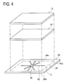
- FIG 4 is a perspective view showing the insulating member 12 and the lid 20 in an exploded state.
- FIGs. 5 and 6 are views showing the insulating member 12 and the lid 20 in a joining state; specifically, FIG 5 is a top view and FIG. 6 is a sectional view taken along a line B-B in FIG 5 .
- the lid 20 is provided with the through hole 40 and grooves 42.
- the lid 20 includes a joining surface 20a to be joined to the insulating member 12 and the other surface 20b opposite the joining surface 20a.
- the surface 20b is located on the side where the fins 18 are placed.
- the through hole 40 is formed through the lid 20 in a pressing direction of the press member 36 (see FIG 3 ) and includes an open end 40a opening in the joining surface 20a, i.e., on the joining surface 20a side, and an open end 40b opening in the other surface 20b, i.e., on the fin 18 side.
- the open end 40b is located in a position corresponding to the gap 22 between the fins 18 in an assembled state as the cooler 10 as shown in FIG 1 .
- the through hole 40 is provided one per insulating member 12 and located near the center of the joining portion 39 between the insulating member 12 and the lid 20.
- FIGs. 4 to 6 the through hole 40 is provided one per insulating member 12 and located near the center of the joining portion 39 between the insulating member 12 and the lid 20.
- the through hole 40 may be provided anywhere in the joining portion 39 between the insulating member 12 and the lid 20 other than the center thereof.
- a plurality of through holes 40 may be provided in one area in the joining portion 39 between the insulating member 12 and the lid 20.
- the grooves 42 are formed in the joining surface 20a of the lid 20 by fine processing using laser or the like.
- the grooves 42 which are one example of a passage communicated with the through hole 40, are arranged to extend radially from the through hole 40 as a center.
- eight grooves 42 in total are arranged in eight positions spaced at equal intervals in a circumferential direction about the center point of the through hole 40.
- the total number of grooves 42 is not limited to eight and, for example, may be appropriately determined according to the area of the joining surface 12b of the insulating member 12 to be joined to the lid 20.
- Each groove 42 is formed between a position X at a predetermined distance apart from an edge 39a of the joining portion 39 between the insulating member 12 and the lid 20 toward the through hole 40 and the position of the through hole 40 as shown in FIGs. 4 to 6 .
- the grooves 42 are not open in positions corresponding to an outer peripheral edge 12a of the insulating member 12.
- a bottom 42a of each groove 42 is sloped downward from the edge 39a of the joining portion 39 between the insulating member 12 and the lid 20 toward the through hole 40. Accordingly, the depth of each groove 42 gradually increases as it approaches the through hole 40.
- the grooves 42 may be designed to each have a uniform depth without making the bottoms 42a slant.
- Example 1 can provide the following operations and effects.
- the brazing material 32 placed between the joining surfaces 12b and the joining surface 20a is guided in the grooves 42 and hence wetted and spread out regularly. Accordingly, the air which may be present in the brazing material 32 is guided in the grooves 42 and passes through the grooves 42, and then released into the cooler 10 through the through holes 40.
- each groove 42 is sloped downward from the edge 39a side of the joining portion 39 between the insulating member 12 and the lid 20 toward the through hole 40 so that the depth of each groove 42 gradually increases as it approaches toward the through hole 40.
- the brazing material 32 has the property of being solidified from a portion located in a small clearance between the joining member and the joined member toward a portion located in a large clearance. Accordingly, the air which may be present in the brazing material 32 is allowed to flow toward a large-depth portion of each groove 42 near the through hole 40 and then be released into the cooler 10 through the through hole 40.
- the open end 40b of the through hole 40 is located on the gap 22 between the fins 18, the air which may be present in the brazing material 32 is released into the gap 22. Thus, no voids are left in the joining layer 24 formed by solidification of the brazing material 32. Therefore, the heat generated from the electronic component 14 stably transferred and released to the cooler 10, so that the electronic component 14 and others can be cooled stably.
- the groove 42 is provided between the position X at the predetermined distance apart from the edge 39a of the joining portion 39 between the insulating member 12 and the lid 20 toward the through hole 40 and the position of the through hole 40.
- the grooves 42 are not open in the positions corresponding to the outer peripheral edge 12a when the insulating member 12 is joined to the lid 20. Consequently, there is no possibility that outside air enters in the grooves 42. This can further ensure that no voids are left in the joining layer 24.
- the grooves 42 are not open in the positions corresponding to the outer peripheral edge 12a of each insulating member 12 during joining of the insulating members 12 to the lid 20. Even in the edge 39a of each joining portion 39, the insulating members 12 and the lid 20 are reliably joined to each other with the brazing material 32. Accordingly, even when thermal stress occurs by the heat applied to the insulating members 12 and the lid 20 during and after joining, the thermal stress does not concentrate on specific portions. Thus, the insulating members 12 and the lid 20 are not disjoined.
- the brazing material 32 held on the interior surface of each through hole 40 by surface tension is solidified, finally, it serves as a stopper that blocks off the through holes 40. Accordingly, there is no possibility that the cooling water flowing through the cooler 10 leaks to the outside through the through holes 40.
- FIGs. 7 and 8 show one insulating member 12 indicated by a chain double-dashed line in FIG 2 to show a joining portion between the insulating member 12 and the lid 20.
- FIG 7 is a perspective view showing the insulating member 12 and the lid 20 in an exploded state.
- FIG 8 is a view showing the insulating member 12 and the lid 20 in a joining state, corresponding to a sectional view taken along a line B-B in FIG 5 .
- a top view of this example is identical to FIG 5 and hence is omitted herein.
- the lid 20 is provided with the through hole 40 and the insulating member 12 is provided with grooves 44.
- the grooves 44 are formed in the joining surface 12b of the insulating member 12 by fine processing using laser or the like.
- the grooves 44 are arranged to extend radially from a position corresponding to the position in which the through hole 40 is located when the insulating member 12 and the lid 20 are joined. Accordingly, the grooves 44 are communicated with the through hole 40 when the insulating member 12 and the lid 20 are joined.
- the grooves 44 are one example of a passage communicated with the through hole 40.
- the through hole 40 is provided in the position corresponding to the center of the insulating member 12 when the insulating member 12 and the lid 20 are joined.
- the grooves 44 are arranged radially from the position near the center of the insulating member 12.
- each insulating member 12 per one insulating member 12, eight grooves 44 in total are arranged in eight positions spaced at equal intervals in a circumferential direction about near the center of the insulating member 12.
- the total number of grooves 44 is not limited to eight and, for example, may be appropriately determined according to the area of the joining surface 12b of the insulating member 12. It is to be noted that the brazing material 32 is placed between the joining surface 12b of the insulating member 12 and the joining surface 20a of the lid 20 as shown in FIG 7 to join the insulating member 12 and the lid 20 to each other.
- Each groove 44 is formed between a position Y at a predetermined distance apart from the outer peripheral edge 12a of the insulating member 12 toward the center and the center position of the insulating member 12, as shown in FIGs. 7 and 8 .
- each groove 44 is sloped upward from the outer peripheral edge 12a toward the center of the insulating member 12. Accordingly, the depth of each groove 44 gradually increases as it approaches the through hole 40.
- the grooves 44 may be designed to each have a uniform depth without making the bottoms 44a slant.
- Example 2 can provide the following operations and effects.
- the brazing material 32 placed between the joining surface 12b and the joining surface 20a is guided in the grooves 44 and hence wetted and spread regularly. Accordingly, the air which may be present in the brazing material 32 is guided in the grooves 44 to pass through the grooves 44, and then released into the cooler 10 through the through hole 40.
- each groove 44 is sloped upward from the outer peripheral edge 12a toward the center of the insulating member 12 so that the depth of each groove 44 gradually increases as it approaches toward the vicinity of the center of the insulating member 12.
- the brazing material 32 has the property of being solidified from a portion located in a small clearance between the joining member and the joined member toward a portion located in a large clearance. Accordingly, the air which may be present in the brazing material 32 is allowed to flow toward a large-depth portion of each groove 44 near the center of the insulating member 12 and then released into the cooler 10 through the through hole 40.
- the open end 40b of the through hole 40 is located on the gap 22 between the fins 18, the air which may be present in the brazing material 32 is released into the gap 22. Thus, no voids are left in the joining layer 24 formed by solidification of the brazing material 32. Therefore, the heat generated from the electronic component 14 can be stably transferred and released to the cooler 10, so that the electronic component 14 and others can be cooled stably.
- the groove 44 is provided between the position Y at the predetermined distance apart from the outer peripheral edge 12a of the insulating member 12 toward the center and the center of the insulating member 12.
- the grooves 44 are not open in the outer peripheral edge 12a. Consequently, there is no possibility that outside air enters in the grooves 44. This can further ensure that no voids are left in the joining layer 24.
- the grooves 44 are not open in the outer peripheral edge 12a and thus the insulating member 12 and the lid 20 are reliably joined to each other with the brazing material 32 even in the edge 39a of the joining portion 39. Accordingly, even when thermal stress occurs by the heat applied to the insulating member 12 and the lid 20 during and after joining, the thermal stress does not concentrate on specific portions. Thus, the insulating member 12 and the lid 20 are not disjoined.
- the brazing material 32 held on the interior surface of each through hole 40 by surface tension is solidified, finally, it serves as a stopper that blocks off the through holes 40. Accordingly, there is no possibility that the cooling water flowing through the cooler 10 leaks to the outside through the through holes 40.
- FIGs. 9 and 10 show one insulating member 12 indicated by a chain double-dashed line in FIG 2 to show a joining portion between the insulating member 12 and the lid 20.
- FIG 9 is a perspective view showing the insulating member 12 and the lid 20 in an exploded state.
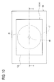
- FIG 10 is a top view showing the insulating member 12 and the lid 20 in a joining state.
- a sectional view taken along a line C-C in FIG 10 is identical to FIG 6 and omitted herein.
- the lid 20 is provided with the through hole 40 and a sloping portion 46.
- the sloping portion 46 is a cone-shaped sloping hollow centered at the through hole 40 as shown in FIG 9 .
- This sloping portion 46 is one example of a passage communicated with the through hole 40 as with the grooves 42 of Example 1 and the grooves 44 of Example 2.
- the sloping portion 46 is provided between a position Z at a predetermined distance apart from the edge 39a of the joining portion 39 between the insulating member 12 and the lid 20 toward the through hole 40 and the position of the through hole 40. Accordingly, the sloping portion 46 is not open in the position corresponding to the outer peripheral edge 12a of the insulating member 12 when the insulating member 12 and the lid 20 are joined.
- Example 3 can provide the following operations and effects.
- the brazing material 32 placed between the joining surface 12b and the joining surface 20a is guided in the sloping portion 46 and hence wetted and spread regularly. Accordingly, the air which may be present in the brazing material 32 is guided in the sloping portion 46 to pass through the sloping portion 46, and then released into the cooler 10 through the through hole 40.
- the sloping portion 46 is sloped downward from the edge 39a of the joining portion 39 between the insulating member 12 and the lid 20 toward the through hole 40 so that the depth of the sloping portion 46 is gradually larger as it approaches toward the through hole 40.
- the brazing material 32 has the property of being solidified from a portion located in a small clearance between the joining member and the joined member to a portion located in a large clearance. Accordingly, the air which may be present in the brazing material 32 is released into the cooler 10 through the through hole 40. Since the open end 40b of the through hole 40 is located on the gap 22 between the fins 18, the air which may be present in the brazing material 32 is released into the gap 22. Thus, no voids are left in the joining layer 24 formed by solidification of the brazing material 32. Therefore, the heat generated from the electronic component 14 can be stably transferred and released to the cooler 10, so that the electronic component 14 and others can be cooled stably.
- the sloping portion 46 is provided between the position Z at the predetermined distance apart from the edge 39a of the joining portion 39 between the insulating member 12 and the lid 20 toward the through hole 40 and the position of the through hole 40.
- the sloping portion 46 is not open in the position corresponding to the outer peripheral edge 12a during joining of the insulating member 12 to the lid 20. Consequently, there is no possibility that outside air enters in the sloping portion 46. This can further ensure that no voids are left in the joining layer 24.
- the brazing material 32 held on the interior surface of each through hole 40 by surface tension is solidified, finally, it serves as a stopper that blocks off the through holes 40. Accordingly, there is no possibility that the cooling water flowing through the cooler 10 leaks to the outside through the through holes 40.
- FIGs. 11 and 12 show one insulating member 12 indicated by a chain double-dashed line in FIG 2 to show a joining portion between the insulating member 12 and the lid 20.
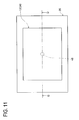
- FIG 11 is a top view
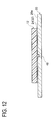
- FIG 12 is a sectional view taken along a line D-D in FIG 10 .
- the lid 20 is provided with a single minute recess 48 near the center of the insulating member 12 when the insulating member 12 and the lid 20 are joined.
- a single recess 50 may be provided near the center of the insulating member 12.
- the position of the recess 48 or the recess 50 is not limited to the vicinity of the center of the insulating member 12. Further, a plurality of such recesses may also be provided.
- Example 4 can provide the following operations and effects.
- the air which may be generated in the joining layer 24 when the brazing material 32 is melted and then solidified from its peripheral portion intensively collects in the recess 48 or 50. This can ensure a joining rate in portions other than the recess 48 or 50. Accordingly, the insulating member 12 and the lid 20 can be joined reliably by brazing.
- the above embodiments are mere examples and do not give any limitations to the present invention.
- the present invention may be embodied in other specific forms without departing from the essential characteristics thereof.
- the insulating member 12 is directly joined to the lid 20 of the cooler 10.
- a metal plate not shown may be interposed between the lid 20 and the insulating member 12.
- the metal plate is formed with grooves, recesses, or the like.
- brazing joining may also be performed between the frame 16 and the lid 20 of the cooler 10 and between the fins 18 and the lid 20 of the cooler 10.
- the present invention may also be applied to a joined member other than the lid 20 of the cooler 10. Furthermore, it may be arranged that the lid 20 of the cooler 10 is provided with the grooves 42 and simultaneously the insulating member 12 is provided with the grooves 44.
Landscapes
- Cooling Or The Like Of Semiconductors Or Solid State Devices (AREA)
- Die Bonding (AREA)
Abstract
Description
- The present invention relates to a semiconductor device including a joining member and a joined member joined to each other by brazing, and a method of producing the semiconductor device.
- For a semiconductor device, when a joining member such as an insulating member (an insulating substrate) is to be joined or bonded by brazing to a member to be joined (a joined member) such as a lid of a cooler, for example, a brazing material placed between the joining member and the joined member is heated to be melted. At that time, if a clearance or gap between the joining member and the joined member is uniform, the melted brazing material is wetted and spread with no regularity. When the brazing material is cooled and solidified to form a joining layer, a peripheral portion of the joining member is apt to become cold first, causing the brazing material to begin solidifying from an outer peripheral edge.
- Thus, air existing in the brazing material is kept in the joining layer. This may leave voids (air layers) with unspecified width or area inside the joining layer. In case such voids are left, it is impossible to stably transfer and release the heat generated in an electronic component such as a semiconductor element to a cooler. Thus, a cooling performance of the cooler could not sufficiently be brought out on the electronic component.
-
Patent document 1 discloses a technique of releasing such air. To be concrete, a pair of electrodes to which an electronic component is to be soldered are formed with guide passages for air release. These guide passages open in a clearance located under the electronic component and in the outside of the electronic component. With this configuration, the air that occurs in the clearance under the electronic component when resin is supplied to form an insulating layer is released through open ends located in the outside of the electronic component via the guide passages. - Patent Document 1:
JP 2007-258605 A - However, in the case where the guide passages are open in the outside of the electronic component as disclosed in
Patent Document 1, outside air is liable to enter from the open ends located in the outside of the electronic component into an insulating layer formed in the clearance under the electronic component through the guide passages. Further, since the brazing material tends to begin solidifying from the outer peripheral edge when the joined member is joined to the joining member by brazing as mentioned above, the air could not be sufficiently released to the outside of the joining member. This results in remaining voids in the insulating layer formed in the clearance under the electronic component. - During joining and after joining between a joining member (e.g., the electronic component in Patent Document 1) and a joined member (e.g., the electrode in Patent Document 1), when heat is added to the joining member and the joined member which are different in linear expansion coefficient, thermal stress occurs. At that time, peeling and cracking are likely to occur particularly in an outer peripheral area of the joining portion. Therefore, in the case where the guide passage is provided to extend up to the outside of the joining portion between the joining member and the joined member as disclosed in
Patent Document 1, thermal stress may concentrate on the guide passage located in the outside of the joining portion, causing deformation of the joining member and the joined member, leading to their disjoining. - The present invention has been made to solve the above problems and has a purpose to provide a semiconductor device and a method of producing the semiconductor device, whereby a joining member and a joined member are joined by brazing without leaving voids in a joining layer.
- To achieve the above purpose, one aspect of the invention provides a semiconductor device including a joining member and a joined member to which the joining member is joined by brazing, wherein the joined member includes a joining surface to be joined to the joining member and a through hole opening in the joining surface, and a passage communicated with the through hole is provided with at least one of a joining surface of the joining member to be joined to the joined member and the joining surface of the joined member to be joined to the joining member.
- According to the above configuration, the joined member is provided with the through hole opening in the joining surface to be joined to the joining member, and the passage communicated with the through hole is provided in at least one of the joining surface of the joining member to be joined to the joined member and the joining surface of the joined member to be joined to the joining member. Accordingly, in brazing the joining member and the joined member, a brazing material is guided in the passage, and wetted and spread with regularity. Thus, air which may be present in the brazing material passes through the passage and is removed through the through hole. Accordingly, the joining member and the joined member can be joined to each other by brazing so that no voids are left in the joining layer formed by solidification of the brazing material.
- In the above configuration, preferably, the passage is provided between a position at a predetermined distance apart from an edge of a joining portion between the joining member and the joined member toward the through hole and a position of the through hole.
- According to the above configuration, the passage is provided between the position at the predetermined distance apart from the edge of the joining portion between the joining member and the joined member toward the through hole and the position of the through hole. Thus, the passage is not open in the position corresponding to the outer peripheral edge of the joining member during joining between the joining member and the joined member. Therefore, there is no possibility that outside air enters in the passage, thus more reliably ensuring that no voids are left in the joining layer.
The joining member and the joined member are joined to each other more reliably with the brazing material. Even when heat is added to the joining member and the joined member during joining and after joining, therefore, the joining member and the joined member are not disjoined. - In the above configuration, preferably, the passage has a depth gradually increasing toward the through hole.
- Herein, the brazing material has the property of being solidified from a portion located in a small clearance to a portion located in a large clearance.
According to the above configuration, therefore, the passage has the depth gradually increasing as it approaches to the through hole. The brazing material will be wetted and spread toward the through hole. Thus, air which may be present in the brazing material is more reliably removed through the through hole. This can further ensure that no voids are left in the joining layer. - In the above configuration, preferably, the passage is a groove.
- According to the above configuration, the brazing material is easy to be guided in the groove, and wetted and spread, thereby allowing air which may be present in the brazing material to easily pass through the groove and be removed through the through hole.
- In the above configuration, preferably, the joined member is a lid member of a cooler for cooling an electronic component placed on the joining member.
- According to the above configuration, no voids are left in the joining layer between the lid member of the cooler and the joining member. Thus, the electronic component placed on the joining member can be more reliably cooled.
- In the above configuration, preferably, the through hole includes an open end that opens in a surface opposite the joining surface and is located on a gap between a plurality of fins provided in the cooler.
- According to the above configuration, the through hole has the open end that opens in the surface opposite the joining surface and is located on the gap between the fins. This makes it possible to release the air which may be present in the brazing material into the cooler. This further ensures that no voids are left in the joining layer.
- To achieve the above object, another aspect of the invention provides a method of producing a semiconductor device including a joining member and a joined member joined to each other by brazing, wherein the joined member is formed with a through hole that opens in a joining surface to be joined to the joining member, a passage communicated with the through hole is provided in at least one of a joining surface of the joining member to be joined to the joined member and the joining surface of the joined member to be joined to the joining member, the method including: placing a brazing material between the joining surface of the joining member to be joined to the joined member and the joining surface of the joined member to be joined to the joining member, and melting and solidifying the brazing material to join the joining member and the joined member to each other.
- According to the above configuration, the joined member is formed with a through hole that opens in a joining surface to be joined to the joining member, a passage communicated with the through hole is provided in at least one of a joining surface of the joining member to be joined to the joined member and the joining surface of the joined member to be joined to the joining member. The method includes: placing a brazing material between the joining surface of the joining member to be joined to the joined member and the joining surface of the joined member to be joined to the joining member, and melting and solidifying the brazing material to join the joining member and the joined member to each other. Therefore, in joining the joining member and the joined member, the brazing material is guided in the passage, and wetted and spread out with regularity. Accordingly, the air which may be present in the brazing material is allowed to pass through the passage and be removed through the through hole. Thus, the joining member and the joined member can be joined by brazing so that no voids are left in the joining layer formed by solidification of the brazing material.
- According to a semiconductor device and a method of producing the semiconductor device according to the present invention, a joining member and a joined member can be joined to each other by brazing without leaving voids in a joining layer.
-
-
FIG 1 is a side view of a semiconductor device of a present invention; -
FIG 2 is a top view showing a state where a cooler and an insulating member are mounted in a brazing jig; -
FIG 3 is a sectional view taken along a line A-A inFIG 2 ; -
FIG 4 is a perspective view showing the insulating member and a lid of the cooler in an exploded state in Example 1; -
FIG 5 is a top view showing the insulating member and the lid of the cooler in a joined state in Example 1; -
FIG 6 is a side view showing the insulating member and the lid of the cooler in the joined state in Example 1; -
FIG 7 is a perspective view showing an insulating member and a lid of a cooler in an exploded state in Example 2; -
FIG 8 is a side view showing the insulating member and the lid of the cooler in a joined state in Example 2; -
FIG 9 is a perspective view showing an insulating member and a lid of a cooler in an exploded state in Example 3; -
FIG 10 is a top view showing the insulating member and the lid of the cooler in a joined state in Example 3; -
FIG 11 is a top view showing an insulating member and a lid of a cooler in a joined state in Example 4; -
FIG 12 is a side view showing the insulating member and the lid of the cooler in the joined state in Example 4; -
FIG 13 is a view showing another example of Example 4. - A detailed description of a preferred embodiment of the present invention will now be given referring to the accompanying drawings.
FIG 1 is a side view of asemiconductor device 1 of the present invention. As shown inFIG 1 , thesemiconductor device 1 includes a cooler 10, insulatingmembers 12,electronic components 14, and others. - The cooler 10 includes a
frame 16, a plurality offins 18,lids 20, and others. Theframe 16 is made of for example aluminum (linear expansion coefficient: about 25 ppm/°C) and formed in a box-like shape. Thefins 18 are arranged in theframe 16 so thatadjacent fins 18 are spaced apart from each other withgaps 22. Thegaps 22 serve as channels of cooling water. - The
lids 20 are made of for example aluminum (linear expansion coefficient: about 25 ppm/°C) and formed in a flat-plate shape. Eachlid 20 is formed with a throughhole 40 as mentioned later. Anopen end 40b of the throughhole 40 opening on thefin 18 side is located in a position to open in agap 22. The throughhole 40 has a size enough to allow passage of air but not allow a brazing material 32 (seeFIG 3 ) held on the interior surface of the throughhole 40 by surface tension to drop out. To be specific, the throughhole 40 has a hole diameter of several millimeters or less. - The insulating
members 12 are insulating substrates placed on thelid 20 of the cooler 10. A linear thermal coefficient of the insulatingmembers 12 is for example 4 to 4.5 ppm/°C. Between the insulatingmembers 12 and thelid 20, joininglayers 24 formed of the solidified brazing material 32 (seeFIG 3 ) are provided. Theelectronic components 14 are semiconductor modules placed on the upper surfaces of the insulatingmembers 12 and are each internally provided with a semiconductor element such as IGBT and a diode to control a large amount of power. - With the above configuration, the
electronic components 14 in thesemiconductor device 1 are cooled in the following manner. Heat generated in eachelectronic component 14 is transferred to thefins 18 via the insulatingmember 12, the joininglayer 24, and thelid 20. At that time, cooling water not shown is supplied through an inlet port 26 (seeFIG 2 ) provided in thelid 20 of the cooler 10. When the cooling water flows in thegaps 22, therefore, heat exchange is performed between the cooling water and thefins 18. Thus, the heat generated in theelectronic components 14 is absorbed by the cooling water. Thereafter, the cooling water absorbing the heat is discharged out through an outlet port 28 (seeFIG 2 ) provided in thelid 20. As above, the heat generated in theelectronic components 14 is released out of thesemiconductor device 1 and theelectronic components 14 are cooled.
In the present embodiment, one example of joining between a joining member and a joined member is explained below as joining between the insulatingmembers 12 and thelid 20. -
FIGs. 2 and3 are views showing a part of a process of producing thesemiconductor device 1, showing a state where the cooler 10 and the insulatingmembers 12 are mounted in abrazing jig 30. Specifically,FIG. 2 is a top view andFIG 3 is a sectional view taken along a line A-A inFIG 2 . InFIG 2 ,press members 36 are not illustrated for convenience of explanation. - As shown in
FIG 2 , four insulatingmembers 12 in total are provided to onecooler 10.
As shown inFIG 3 , the insulatingmembers 12 are placed on thelid 20 by interposing the brazing material 32 (a metal joining material and so on) and further thepress members 36 supported in thebrazing jig 30 are disposed respectively on the insulatingmembers 12.
Thebrazing jig 30 has for example anouter frame 38 having a box-like shape as shown inFIG 3 and is configured to place the cooler 10 inside theouter frame 38. - The
brazing jig 30 configured as above, in which the cooler 10 and the insulatingmembers 12 are mounted, is put in a heating furnace not shown. An internal temperature of the heating furnace is increased to a melting temperature of thebrazing material 32 or higher, thereby melting thebrazing material 32, and then is decreased to the melting temperature of thebrazing material 32 or lower. Accordingly, thebrazing material 32 is melted once, wetted and spread in clearances between the insulatingmembers 12 and thelid 20 and then solidified, forming the joining layers 24 (seeFIG 1 ). Thus, the insulatingmembers 12 and thelid 20 are joined or bonded to one another by brazing. - Therefore, the following explanation is given to examples of the present invention related to the above joining between the insulating
members 12 and thelid 20 of the cooler 10 by brazing. - In Example 1,
FIGs. 4 to 6 show one insulatingmember 12 indicated by a chain double-dashed line inFIG 2 to show a joiningportion 39 between the insulatingmember 12 and thelid 20. Specifically,FIG 4 is a perspective view showing the insulatingmember 12 and thelid 20 in an exploded state.FIGs. 5 and6 are views showing the insulatingmember 12 and thelid 20 in a joining state; specifically,FIG 5 is a top view andFIG. 6 is a sectional view taken along a line B-B inFIG 5 . - As shown in
FIGs. 4 to 6 , thelid 20 is provided with the throughhole 40 andgrooves 42. Thelid 20 includes a joiningsurface 20a to be joined to the insulatingmember 12 and theother surface 20b opposite the joiningsurface 20a. Thesurface 20b is located on the side where thefins 18 are placed. - The through
hole 40 is formed through thelid 20 in a pressing direction of the press member 36 (seeFIG 3 ) and includes anopen end 40a opening in the joiningsurface 20a, i.e., on the joiningsurface 20a side, and anopen end 40b opening in theother surface 20b, i.e., on thefin 18 side. Theopen end 40b is located in a position corresponding to thegap 22 between thefins 18 in an assembled state as the cooler 10 as shown inFIG 1 . In the example shown inFIGs. 4 to 6 , the throughhole 40 is provided one per insulatingmember 12 and located near the center of the joiningportion 39 between the insulatingmember 12 and thelid 20. However, not limited to the example shown inFIGs. 4 to 6 , the throughhole 40 may be provided anywhere in the joiningportion 39 between the insulatingmember 12 and thelid 20 other than the center thereof. As an alternative, a plurality of throughholes 40 may be provided in one area in the joiningportion 39 between the insulatingmember 12 and thelid 20. - The
grooves 42 are formed in the joiningsurface 20a of thelid 20 by fine processing using laser or the like. Thegrooves 42, which are one example of a passage communicated with the throughhole 40, are arranged to extend radially from the throughhole 40 as a center. In the example shown inFIGs. 4 to 6 , for one throughhole 40, eightgrooves 42 in total are arranged in eight positions spaced at equal intervals in a circumferential direction about the center point of the throughhole 40. The total number ofgrooves 42 is not limited to eight and, for example, may be appropriately determined according to the area of the joiningsurface 12b of the insulatingmember 12 to be joined to thelid 20. - Each
groove 42 is formed between a position X at a predetermined distance apart from anedge 39a of the joiningportion 39 between the insulatingmember 12 and thelid 20 toward the throughhole 40 and the position of the throughhole 40 as shown inFIGs. 4 to 6 . Thus, when the insulatingmember 12 is to be joined to thelid 20, thegrooves 42 are not open in positions corresponding to an outerperipheral edge 12a of the insulatingmember 12.
As shown inFIG 6 , furthermore, a bottom 42a of eachgroove 42 is sloped downward from theedge 39a of the joiningportion 39 between the insulatingmember 12 and thelid 20 toward the throughhole 40. Accordingly, the depth of eachgroove 42 gradually increases as it approaches the throughhole 40. Alternatively, thegrooves 42 may be designed to each have a uniform depth without making thebottoms 42a slant. - The above configuration in Example 1 can provide the following operations and effects.
During melting and solidifying, thebrazing material 32 placed between the joiningsurfaces 12b and the joiningsurface 20a is guided in thegrooves 42 and hence wetted and spread out regularly. Accordingly, the air which may be present in thebrazing material 32 is guided in thegrooves 42 and passes through thegrooves 42, and then released into the cooler 10 through the through holes 40. - Especially, the bottom 42a of each
groove 42 is sloped downward from theedge 39a side of the joiningportion 39 between the insulatingmember 12 and thelid 20 toward the throughhole 40 so that the depth of eachgroove 42 gradually increases as it approaches toward the throughhole 40. Herein, thebrazing material 32 has the property of being solidified from a portion located in a small clearance between the joining member and the joined member toward a portion located in a large clearance. Accordingly, the air which may be present in thebrazing material 32 is allowed to flow toward a large-depth portion of eachgroove 42 near the throughhole 40 and then be released into the cooler 10 through the throughhole 40. Since theopen end 40b of the throughhole 40 is located on thegap 22 between thefins 18, the air which may be present in thebrazing material 32 is released into thegap 22. Thus, no voids are left in the joininglayer 24 formed by solidification of thebrazing material 32. Therefore, the heat generated from theelectronic component 14 stably transferred and released to the cooler 10, so that theelectronic component 14 and others can be cooled stably. - Further, the
groove 42 is provided between the position X at the predetermined distance apart from theedge 39a of the joiningportion 39 between the insulatingmember 12 and thelid 20 toward the throughhole 40 and the position of the throughhole 40. Thus, thegrooves 42 are not open in the positions corresponding to the outerperipheral edge 12a when the insulatingmember 12 is joined to thelid 20. Consequently, there is no possibility that outside air enters in thegrooves 42. This can further ensure that no voids are left in the joininglayer 24. - Furthermore, the
grooves 42 are not open in the positions corresponding to the outerperipheral edge 12a of each insulatingmember 12 during joining of the insulatingmembers 12 to thelid 20. Even in theedge 39a of each joiningportion 39, the insulatingmembers 12 and thelid 20 are reliably joined to each other with thebrazing material 32. Accordingly, even when thermal stress occurs by the heat applied to the insulatingmembers 12 and thelid 20 during and after joining, the thermal stress does not concentrate on specific portions. Thus, the insulatingmembers 12 and thelid 20 are not disjoined.
When thebrazing material 32 held on the interior surface of each throughhole 40 by surface tension is solidified, finally, it serves as a stopper that blocks off the through holes 40. Accordingly, there is no possibility that the cooling water flowing through the cooler 10 leaks to the outside through the through holes 40. - In Example 2,
FIGs. 7 and8 show one insulatingmember 12 indicated by a chain double-dashed line inFIG 2 to show a joining portion between the insulatingmember 12 and thelid 20. Specifically,FIG 7 is a perspective view showing the insulatingmember 12 and thelid 20 in an exploded state.FIG 8 is a view showing the insulatingmember 12 and thelid 20 in a joining state, corresponding to a sectional view taken along a line B-B inFIG 5 . A top view of this example is identical toFIG 5 and hence is omitted herein. - As shown in
FIGs. 7 and8 , thelid 20 is provided with the throughhole 40 and the insulatingmember 12 is provided withgrooves 44.
In this example, the details of the throughhole 40 are identical to those in Example 1 and omitted herein.
Thegrooves 44 are formed in the joiningsurface 12b of the insulatingmember 12 by fine processing using laser or the like. Thegrooves 44 are arranged to extend radially from a position corresponding to the position in which the throughhole 40 is located when the insulatingmember 12 and thelid 20 are joined. Accordingly, thegrooves 44 are communicated with the throughhole 40 when the insulatingmember 12 and thelid 20 are joined. As above, thegrooves 44 are one example of a passage communicated with the throughhole 40. - In the example shown in
FIG. 7 , the throughhole 40 is provided in the position corresponding to the center of the insulatingmember 12 when the insulatingmember 12 and thelid 20 are joined. Thus, thegrooves 44 are arranged radially from the position near the center of the insulatingmember 12. - In the example shown in
FIG 7 , per one insulatingmember 12, eightgrooves 44 in total are arranged in eight positions spaced at equal intervals in a circumferential direction about near the center of the insulatingmember 12. The total number ofgrooves 44 is not limited to eight and, for example, may be appropriately determined according to the area of the joiningsurface 12b of the insulatingmember 12.
It is to be noted that thebrazing material 32 is placed between the joiningsurface 12b of the insulatingmember 12 and the joiningsurface 20a of thelid 20 as shown inFIG 7 to join the insulatingmember 12 and thelid 20 to each other. - Each
groove 44 is formed between a position Y at a predetermined distance apart from the outerperipheral edge 12a of the insulatingmember 12 toward the center and the center position of the insulatingmember 12, as shown inFIGs. 7 and8 . This means that thegroove 44 is provided between the position Y at the predetermined distance apart from the outerperipheral edge 12a of the insulatingmember 12 toward the throughhole 40 and the position of the throughhole 40 as shown inFIG 8 . Accordingly, thegrooves 44 are not open in the outerperipheral edge 12a of the insulatingmember 12. - Furthermore, as shown in
FIG. 8 , a bottom 44a of each groove is sloped upward from the outerperipheral edge 12a toward the center of the insulatingmember 12. Accordingly, the depth of eachgroove 44 gradually increases as it approaches the throughhole 40. As an alternative, thegrooves 44 may be designed to each have a uniform depth without making thebottoms 44a slant. - The above configuration in Example 2 can provide the following operations and effects.
During melting and solidifying, thebrazing material 32 placed between the joiningsurface 12b and the joiningsurface 20a is guided in thegrooves 44 and hence wetted and spread regularly. Accordingly, the air which may be present in thebrazing material 32 is guided in thegrooves 44 to pass through thegrooves 44, and then released into the cooler 10 through the throughhole 40. - Especially, the bottom 44a of each
groove 44 is sloped upward from the outerperipheral edge 12a toward the center of the insulatingmember 12 so that the depth of eachgroove 44 gradually increases as it approaches toward the vicinity of the center of the insulatingmember 12. Herein, thebrazing material 32 has the property of being solidified from a portion located in a small clearance between the joining member and the joined member toward a portion located in a large clearance. Accordingly, the air which may be present in thebrazing material 32 is allowed to flow toward a large-depth portion of eachgroove 44 near the center of the insulatingmember 12 and then released into the cooler 10 through the throughhole 40. Since theopen end 40b of the throughhole 40 is located on thegap 22 between thefins 18, the air which may be present in thebrazing material 32 is released into thegap 22. Thus, no voids are left in the joininglayer 24 formed by solidification of thebrazing material 32. Therefore, the heat generated from theelectronic component 14 can be stably transferred and released to the cooler 10, so that theelectronic component 14 and others can be cooled stably. - Further, the
groove 44 is provided between the position Y at the predetermined distance apart from the outerperipheral edge 12a of the insulatingmember 12 toward the center and the center of the insulatingmember 12. Thus, thegrooves 44 are not open in the outerperipheral edge 12a. Consequently, there is no possibility that outside air enters in thegrooves 44. This can further ensure that no voids are left in the joininglayer 24. - Furthermore, the
grooves 44 are not open in the outerperipheral edge 12a and thus the insulatingmember 12 and thelid 20 are reliably joined to each other with thebrazing material 32 even in theedge 39a of the joiningportion 39. Accordingly, even when thermal stress occurs by the heat applied to the insulatingmember 12 and thelid 20 during and after joining, the thermal stress does not concentrate on specific portions. Thus, the insulatingmember 12 and thelid 20 are not disjoined.
When thebrazing material 32 held on the interior surface of each throughhole 40 by surface tension is solidified, finally, it serves as a stopper that blocks off the through holes 40. Accordingly, there is no possibility that the cooling water flowing through the cooler 10 leaks to the outside through the through holes 40. - In Example 3,
FIGs. 9 and10 show one insulatingmember 12 indicated by a chain double-dashed line inFIG 2 to show a joining portion between the insulatingmember 12 and thelid 20. Specifically,FIG 9 is a perspective view showing the insulatingmember 12 and thelid 20 in an exploded state.FIG 10 is a top view showing the insulatingmember 12 and thelid 20 in a joining state. A sectional view taken along a line C-C inFIG 10 is identical toFIG 6 and omitted herein. - As shown in
FIGs. 9 and10 , thelid 20 is provided with the throughhole 40 and a slopingportion 46.
In this example, the details of the throughhole 40 are identical to those in Example 1 or Example 2 and omitted herein.
The slopingportion 46 is a cone-shaped sloping hollow centered at the throughhole 40 as shown inFIG 9 . This slopingportion 46 is one example of a passage communicated with the throughhole 40 as with thegrooves 42 of Example 1 and thegrooves 44 of Example 2. The slopingportion 46 is provided between a position Z at a predetermined distance apart from theedge 39a of the joiningportion 39 between the insulatingmember 12 and thelid 20 toward the throughhole 40 and the position of the throughhole 40. Accordingly, the slopingportion 46 is not open in the position corresponding to the outerperipheral edge 12a of the insulatingmember 12 when the insulatingmember 12 and thelid 20 are joined. - The above configuration in Example 3 can provide the following operations and effects.
During melting and solidifying, thebrazing material 32 placed between the joiningsurface 12b and the joiningsurface 20a is guided in the slopingportion 46 and hence wetted and spread regularly. Accordingly, the air which may be present in thebrazing material 32 is guided in the slopingportion 46 to pass through the slopingportion 46, and then released into the cooler 10 through the throughhole 40. - Especially, the sloping
portion 46 is sloped downward from theedge 39a of the joiningportion 39 between the insulatingmember 12 and thelid 20 toward the throughhole 40 so that the depth of the slopingportion 46 is gradually larger as it approaches toward the throughhole 40. Herein, thebrazing material 32 has the property of being solidified from a portion located in a small clearance between the joining member and the joined member to a portion located in a large clearance. Accordingly, the air which may be present in thebrazing material 32 is released into the cooler 10 through the throughhole 40. Since theopen end 40b of the throughhole 40 is located on thegap 22 between thefins 18, the air which may be present in thebrazing material 32 is released into thegap 22. Thus, no voids are left in the joininglayer 24 formed by solidification of thebrazing material 32. Therefore, the heat generated from theelectronic component 14 can be stably transferred and released to the cooler 10, so that theelectronic component 14 and others can be cooled stably. - Further, the sloping
portion 46 is provided between the position Z at the predetermined distance apart from theedge 39a of the joiningportion 39 between the insulatingmember 12 and thelid 20 toward the throughhole 40 and the position of the throughhole 40. Thus, the slopingportion 46 is not open in the position corresponding to the outerperipheral edge 12a during joining of the insulatingmember 12 to thelid 20. Consequently, there is no possibility that outside air enters in the slopingportion 46. This can further ensure that no voids are left in the joininglayer 24.
Furthermore, as in Examples 1 and 2, when thebrazing material 32 held on the interior surface of each throughhole 40 by surface tension is solidified, finally, it serves as a stopper that blocks off the through holes 40. Accordingly, there is no possibility that the cooling water flowing through the cooler 10 leaks to the outside through the through holes 40. - In Example 4,
FIGs. 11 and12 show one insulatingmember 12 indicated by a chain double-dashed line inFIG 2 to show a joining portion between the insulatingmember 12 and thelid 20. Specifically,FIG 11 is a top view andFIG 12 is a sectional view taken along a line D-D inFIG 10 . - As shown in
FIGs. 11 and12 , thelid 20 is provided with asingle minute recess 48 near the center of the insulatingmember 12 when the insulatingmember 12 and thelid 20 are joined. As an alternative, as shown inFIG 13 , asingle recess 50 may be provided near the center of the insulatingmember 12. The position of therecess 48 or therecess 50 is not limited to the vicinity of the center of the insulatingmember 12. Further, a plurality of such recesses may also be provided. - The above configuration in Example 4 can provide the following operations and effects.
The air which may be generated in the joininglayer 24 when thebrazing material 32 is melted and then solidified from its peripheral portion intensively collects in therecess recess member 12 and thelid 20 can be joined reliably by brazing. - The above embodiments are mere examples and do not give any limitations to the present invention. The present invention may be embodied in other specific forms without departing from the essential characteristics thereof.
In the above examples, the insulatingmember 12 is directly joined to thelid 20 of the cooler 10. As an alternative, a metal plate not shown may be interposed between thelid 20 and the insulatingmember 12. In this case, instead of the insulatingmember 12, the metal plate is formed with grooves, recesses, or the like. - At the same time as joining between the insulating
member 12 and thelid 20 of the cooler 10 in the aforementioned Examples 1 to 4, brazing joining may also be performed between theframe 16 and thelid 20 of the cooler 10 and between thefins 18 and thelid 20 of the cooler 10.
The present invention may also be applied to a joined member other than thelid 20 of the cooler 10.
Furthermore, it may be arranged that thelid 20 of the cooler 10 is provided with thegrooves 42 and simultaneously the insulatingmember 12 is provided with thegrooves 44. -
- 1
- Semiconductor device
- 10
- Cooler
- 12
- Insulating member
- 12a
- Outer peripheral edge
- 12b
- Joining surface
- 14
- Electronic component
- 18
- Fin
- 20
- Lid
- 20a
- Joining surface
- 20b
- Surface
- 22
- Gap
- 24
- Joining layer
- 32
- Brazing material
- 39
- Joining portion
- 39a
- Edge
- 40
- Through hole
- 40a
- Open end
- 40b
- Open end
- 42
- Groove
- 42a
- Bottom
- 44
- Groove
- 44a
- Bottom
- 46
- Sloping portion
- 48
- Recess
- 50
- Recess
Claims (7)
- A semiconductor device including a joining member and a joined member to which the joining member is joined by brazing, wherein
the joined member includes a joining surface to be joined to the joining member and a through hole opening in the joining surface, and
a passage communicated with the through hole is provided with at least one of a joining surface of the joining member to be joined to the joined member and the joining surface of the joined member to be joined to the joining member. - The semiconductor device according to claim 1, wherein the passage is provided between a position at a predetermined distance apart from an edge of a joining portion between the joining member and the joined member toward the through hole and a position of the through hole.
- The semiconductor device according to claim 1 or 2, wherein the passage has a depth gradually increasing toward the through hole.
- The semiconductor device according to any one of claims 1 to 3, wherein the passage is a groove.
- The semiconductor device according to any one of claims 1 to 4, wherein the joined member is a lid member of a cooler for cooling an electronic component placed on the joining member.
- The semiconductor device according to claim 5, wherein the through hole includes an open end that opens in a surface opposite the joining surface and is located on a gap between a plurality of fins provided in the cooler.
- A method of producing a semiconductor device including a joining member and a joined member joined to each other by brazing, wherein
the joined member is formed with a through hole that opens in a joining surface to be joined to the joining member,
a passage communicated with the through hole is provided in at least one of a joining surface of the joining member to be joined to the joined member and the joining surface of the joined member to be joined to the joining member,
the method including:placing a brazing material between the joining surface of the joining member to be joined to the joined member and the joining surface of the joined member to be joined to the joining member, andmelting and solidifying the brazing material to join the joining member and the joined member to each other.
Applications Claiming Priority (1)
| Application Number | Priority Date | Filing Date | Title |
|---|---|---|---|
| PCT/JP2009/070008 WO2011064873A1 (en) | 2009-11-27 | 2009-11-27 | Semiconductor device and method of producing same |
Publications (2)
| Publication Number | Publication Date |
|---|---|
| EP2506299A1 true EP2506299A1 (en) | 2012-10-03 |
| EP2506299A4 EP2506299A4 (en) | 2014-09-17 |
Family
ID=44065992
Family Applications (1)
| Application Number | Title | Priority Date | Filing Date |
|---|---|---|---|
| EP09851664.4A Withdrawn EP2506299A4 (en) | 2009-11-27 | 2009-11-27 | SEMICONDUCTOR DEVICE AND METHOD FOR MANUFACTURING THE SAME |
Country Status (5)
| Country | Link |
|---|---|
| US (1) | US8916964B2 (en) |
| EP (1) | EP2506299A4 (en) |
| JP (1) | JP5549678B2 (en) |
| CN (1) | CN102656684B (en) |
| WO (1) | WO2011064873A1 (en) |
Families Citing this family (3)
| Publication number | Priority date | Publication date | Assignee | Title |
|---|---|---|---|---|
| CN105247666B (en) * | 2013-07-10 | 2017-12-01 | 三菱电机株式会社 | Semiconductor device and its manufacture method |
| CN103824824B (en) * | 2014-03-03 | 2017-01-04 | 中国科学院微电子研究所 | An integrated heat dissipation structure and its manufacturing method |
| JP7039917B2 (en) * | 2017-10-06 | 2022-03-23 | 富士電機株式会社 | Cooler |
Family Cites Families (15)
| Publication number | Priority date | Publication date | Assignee | Title |
|---|---|---|---|---|
| JPH01161892A (en) * | 1987-12-18 | 1989-06-26 | Toshiba Corp | Ceramics circuit board and its manufacture |
| JPH09275170A (en) | 1996-04-03 | 1997-10-21 | Fuji Electric Co Ltd | Semiconductor device |
| JP2919387B2 (en) * | 1996-09-26 | 1999-07-12 | 山形日本電気株式会社 | High frequency characteristics measurement jig |
| US6414867B2 (en) * | 2000-02-16 | 2002-07-02 | Hitachi, Ltd. | Power inverter |
| JP2002280503A (en) | 2001-03-16 | 2002-09-27 | Unisia Jecs Corp | Semiconductor device |
| US7078803B2 (en) * | 2002-09-27 | 2006-07-18 | Isothermal Systems Research, Inc. | Integrated circuit heat dissipation system |
| JP2006057930A (en) * | 2004-08-20 | 2006-03-02 | Denso Corp | Vehicle radiator |
| JP5000105B2 (en) * | 2005-06-28 | 2012-08-15 | ローム株式会社 | Semiconductor device |
| KR101384426B1 (en) * | 2006-03-13 | 2014-04-10 | 쇼와 덴코 가부시키가이샤 | Base for power module |
| JP2007258605A (en) | 2006-03-24 | 2007-10-04 | Toshiba Corp | Printed wiring board with built-in component, manufacturing method of printed wiring board with built-in component, and electronic device |
| JP2008159914A (en) * | 2006-12-25 | 2008-07-10 | Toyota Industries Corp | Method for mounting component |
| JP4994123B2 (en) | 2007-06-18 | 2012-08-08 | ニチコン株式会社 | Power semiconductor module |
| JP2009016659A (en) * | 2007-07-06 | 2009-01-22 | Denso Corp | Component connection structure and component connection method |
| JP5117270B2 (en) * | 2008-04-25 | 2013-01-16 | シャープ株式会社 | WIRING BOARD, SEMICONDUCTOR DEVICE, AND METHOD FOR MANUFACTURING SEMICONDUCTOR DEVICE |
| JP5757086B2 (en) * | 2008-10-29 | 2015-07-29 | 日本電気株式会社 | COOLING STRUCTURE, ELECTRONIC DEVICE, AND COOLING METHOD |
-
2009
- 2009-11-27 JP JP2011543051A patent/JP5549678B2/en not_active Expired - Fee Related
- 2009-11-27 WO PCT/JP2009/070008 patent/WO2011064873A1/en not_active Ceased
- 2009-11-27 EP EP09851664.4A patent/EP2506299A4/en not_active Withdrawn
- 2009-11-27 US US13/511,543 patent/US8916964B2/en not_active Expired - Fee Related
- 2009-11-27 CN CN200980162622.1A patent/CN102656684B/en not_active Expired - Fee Related
Also Published As
| Publication number | Publication date |
|---|---|
| US20120280383A1 (en) | 2012-11-08 |
| CN102656684A (en) | 2012-09-05 |
| JPWO2011064873A1 (en) | 2013-04-11 |
| US8916964B2 (en) | 2014-12-23 |
| EP2506299A4 (en) | 2014-09-17 |
| JP5549678B2 (en) | 2014-07-16 |
| CN102656684B (en) | 2015-02-04 |
| WO2011064873A1 (en) | 2011-06-03 |
Similar Documents
| Publication | Publication Date | Title |
|---|---|---|
| US8371367B2 (en) | Heat sink and fabricating method of the same | |
| EP3734646B1 (en) | Semiconductor component, motor vehicle and method for producing a semiconductor component | |
| US8199505B2 (en) | Jet impingement heat exchanger apparatuses and power electronics modules | |
| US8299606B2 (en) | Semiconductor device includes a ceramic substrate and heat sink | |
| EP2200080B1 (en) | Low Cost Manufacturing of Micro-Channel Heatsink | |
| US20050280142A1 (en) | Electronic assembly having an indium wetting layer on a thermally conductive body | |
| US9087778B2 (en) | Joining method and semiconductor device manufacturing method | |
| EP2432012A1 (en) | Heat exchanger, semiconductor device, method for manufacturing the heat exchanger, and method for manufacturing the semiconductor device | |
| EP2541594A1 (en) | Semiconductor module manufacturing method, semiconductor module, and manufacturing device | |
| JP6554406B2 (en) | Liquid-cooled cooler | |
| EP2442358A1 (en) | Semiconductor device | |
| WO2014013764A1 (en) | Heater for bonding device and method for cooling same | |
| CN107000092A (en) | For the heat transfer unit (HTU) for the welded connection for manufacturing electronic unit | |
| US8916964B2 (en) | Semiconductor device and method of producing same | |
| US20200091035A1 (en) | Module base with integrated thermal spreader and heat sink for thermal and structural management of high-performance integrated circuits or other devices | |
| US20210247151A1 (en) | Fluid-based cooling device for cooling at least two distinct first heat-generating elements of a heat source assembly | |
| CN102751249B (en) | Heat radiator and manufacturing method thereof | |
| EP1954110A1 (en) | Soldering apparatus and soldering method | |
| JP2007019365A (en) | Micro heat sink and jacket using the same | |
| JP4275938B2 (en) | Method for manufacturing thermoelectric conversion module | |
| KR102566368B1 (en) | Semiconductor device thermal management module and manufacturing method thereof | |
| KR100826052B1 (en) | Case bonding method and apparatus of plate heat transfer apparatus | |
| JP4232727B2 (en) | Semiconductor device and manufacturing method thereof | |
| JP2026005941A (en) | Semiconductor device manufacturing method and semiconductor device | |
| JP2018019000A (en) | Power semiconductor module |
Legal Events
| Date | Code | Title | Description |
|---|---|---|---|
| PUAI | Public reference made under article 153(3) epc to a published international application that has entered the european phase |
Free format text: ORIGINAL CODE: 0009012 |
|
| 17P | Request for examination filed |
Effective date: 20120330 |
|
| AK | Designated contracting states |
Kind code of ref document: A1 Designated state(s): AT BE BG CH CY CZ DE DK EE ES FI FR GB GR HR HU IE IS IT LI LT LU LV MC MK MT NL NO PL PT RO SE SI SK SM TR |
|
| RAP1 | Party data changed (applicant data changed or rights of an application transferred) |
Owner name: TOYOTA JIDOSHA KABUSHIKI KAISHA |
|
| DAX | Request for extension of the european patent (deleted) | ||
| A4 | Supplementary search report drawn up and despatched |
Effective date: 20140821 |
|
| RIC1 | Information provided on ipc code assigned before grant |
Ipc: H01L 23/473 20060101ALI20140814BHEP Ipc: H01L 21/48 20060101ALI20140814BHEP Ipc: H01L 23/00 20060101AFI20140814BHEP |
|
| GRAP | Despatch of communication of intention to grant a patent |
Free format text: ORIGINAL CODE: EPIDOSNIGR1 |
|
| STAA | Information on the status of an ep patent application or granted ep patent |
Free format text: STATUS: GRANT OF PATENT IS INTENDED |
|
| INTG | Intention to grant announced |
Effective date: 20180327 |
|
| RIN1 | Information on inventor provided before grant (corrected) |
Inventor name: MORINO MASAHIRO Inventor name: TATEBE KATSUHIKO Inventor name: TAKENAGA TOMOHIRO Inventor name: KAKIUCHI EISAKU Inventor name: TAKETSUNA YASUJI |
|
| STAA | Information on the status of an ep patent application or granted ep patent |
Free format text: STATUS: THE APPLICATION IS DEEMED TO BE WITHDRAWN |
|
| 18D | Application deemed to be withdrawn |
Effective date: 20180807 |