EP2503693A1 - Composite Semiconductor Device with Active Oscillation Prevention - Google Patents
Composite Semiconductor Device with Active Oscillation Prevention Download PDFInfo
- Publication number
- EP2503693A1 EP2503693A1 EP12159776A EP12159776A EP2503693A1 EP 2503693 A1 EP2503693 A1 EP 2503693A1 EP 12159776 A EP12159776 A EP 12159776A EP 12159776 A EP12159776 A EP 12159776A EP 2503693 A1 EP2503693 A1 EP 2503693A1
- Authority
- EP
- European Patent Office
- Prior art keywords
- iii
- semiconductor device
- transistor
- composite semiconductor
- composite
- Prior art date
- Legal status (The legal status is an assumption and is not a legal conclusion. Google has not performed a legal analysis and makes no representation as to the accuracy of the status listed.)
- Granted
Links
Images

Classifications
-
- H—ELECTRICITY
- H10—SEMICONDUCTOR DEVICES; ELECTRIC SOLID-STATE DEVICES NOT OTHERWISE PROVIDED FOR
- H10D—INORGANIC ELECTRIC SEMICONDUCTOR DEVICES
- H10D84/00—Integrated devices formed in or on semiconductor substrates that comprise only semiconducting layers, e.g. on Si wafers or on GaAs-on-Si wafers
- H10D84/80—Integrated devices formed in or on semiconductor substrates that comprise only semiconducting layers, e.g. on Si wafers or on GaAs-on-Si wafers characterised by the integration of at least one component covered by groups H10D12/00 or H10D30/00, e.g. integration of IGFETs
- H10D84/82—Integrated devices formed in or on semiconductor substrates that comprise only semiconducting layers, e.g. on Si wafers or on GaAs-on-Si wafers characterised by the integration of at least one component covered by groups H10D12/00 or H10D30/00, e.g. integration of IGFETs of only field-effect components
-
- H—ELECTRICITY
- H03—ELECTRONIC CIRCUITRY
- H03K—PULSE TECHNIQUE
- H03K17/00—Electronic switching or gating, i.e. not by contact-making and –breaking
- H03K17/10—Modifications for increasing the maximum permissible switched voltage
- H03K17/107—Modifications for increasing the maximum permissible switched voltage in composite switches
-
- H—ELECTRICITY
- H03—ELECTRONIC CIRCUITRY
- H03K—PULSE TECHNIQUE
- H03K17/00—Electronic switching or gating, i.e. not by contact-making and –breaking
- H03K17/16—Modifications for eliminating interference voltages or currents
- H03K17/168—Modifications for eliminating interference voltages or currents in composite switches
-
- H—ELECTRICITY
- H03—ELECTRONIC CIRCUITRY
- H03K—PULSE TECHNIQUE
- H03K17/00—Electronic switching or gating, i.e. not by contact-making and –breaking
- H03K17/51—Electronic switching or gating, i.e. not by contact-making and –breaking characterised by the components used
- H03K17/56—Electronic switching or gating, i.e. not by contact-making and –breaking characterised by the components used by the use, as active elements, of semiconductor devices
- H03K17/567—Circuits characterised by the use of more than one type of semiconductor device, e.g. BIMOS, composite devices such as IGBT
-
- H—ELECTRICITY
- H10—SEMICONDUCTOR DEVICES; ELECTRIC SOLID-STATE DEVICES NOT OTHERWISE PROVIDED FOR
- H10D—INORGANIC ELECTRIC SEMICONDUCTOR DEVICES
- H10D30/00—Field-effect transistors [FET]
- H10D30/60—Insulated-gate field-effect transistors [IGFET]
-
- H—ELECTRICITY
- H10—SEMICONDUCTOR DEVICES; ELECTRIC SOLID-STATE DEVICES NOT OTHERWISE PROVIDED FOR
- H10D—INORGANIC ELECTRIC SEMICONDUCTOR DEVICES
- H10D62/00—Semiconductor bodies, or regions thereof, of devices having potential barriers
- H10D62/80—Semiconductor bodies, or regions thereof, of devices having potential barriers characterised by the materials
- H10D62/83—Semiconductor bodies, or regions thereof, of devices having potential barriers characterised by the materials being Group IV materials, e.g. B-doped Si or undoped Ge
-
- H—ELECTRICITY
- H10—SEMICONDUCTOR DEVICES; ELECTRIC SOLID-STATE DEVICES NOT OTHERWISE PROVIDED FOR
- H10D—INORGANIC ELECTRIC SEMICONDUCTOR DEVICES
- H10D62/00—Semiconductor bodies, or regions thereof, of devices having potential barriers
- H10D62/80—Semiconductor bodies, or regions thereof, of devices having potential barriers characterised by the materials
- H10D62/85—Semiconductor bodies, or regions thereof, of devices having potential barriers characterised by the materials being Group III-V materials, e.g. GaAs
- H10D62/8503—Nitride Group III-V materials, e.g. AlN or GaN
-
- H—ELECTRICITY
- H10—SEMICONDUCTOR DEVICES; ELECTRIC SOLID-STATE DEVICES NOT OTHERWISE PROVIDED FOR
- H10D—INORGANIC ELECTRIC SEMICONDUCTOR DEVICES
- H10D84/00—Integrated devices formed in or on semiconductor substrates that comprise only semiconducting layers, e.g. on Si wafers or on GaAs-on-Si wafers
- H10D84/01—Manufacture or treatment
- H10D84/0123—Integrating together multiple components covered by H10D12/00 or H10D30/00, e.g. integrating multiple IGBTs
- H10D84/0126—Integrating together multiple components covered by H10D12/00 or H10D30/00, e.g. integrating multiple IGBTs the components including insulated gates, e.g. IGFETs
- H10D84/0163—Integrating together multiple components covered by H10D12/00 or H10D30/00, e.g. integrating multiple IGBTs the components including insulated gates, e.g. IGFETs the components including enhancement-mode IGFETs and depletion-mode IGFETs
-
- H—ELECTRICITY
- H10—SEMICONDUCTOR DEVICES; ELECTRIC SOLID-STATE DEVICES NOT OTHERWISE PROVIDED FOR
- H10D—INORGANIC ELECTRIC SEMICONDUCTOR DEVICES
- H10D84/00—Integrated devices formed in or on semiconductor substrates that comprise only semiconducting layers, e.g. on Si wafers or on GaAs-on-Si wafers
- H10D84/01—Manufacture or treatment
- H10D84/02—Manufacture or treatment characterised by using material-based technologies
- H10D84/03—Manufacture or treatment characterised by using material-based technologies using Group IV technology, e.g. silicon technology or silicon-carbide [SiC] technology
- H10D84/038—Manufacture or treatment characterised by using material-based technologies using Group IV technology, e.g. silicon technology or silicon-carbide [SiC] technology using silicon technology, e.g. SiGe
-
- H—ELECTRICITY
- H10—SEMICONDUCTOR DEVICES; ELECTRIC SOLID-STATE DEVICES NOT OTHERWISE PROVIDED FOR
- H10D—INORGANIC ELECTRIC SEMICONDUCTOR DEVICES
- H10D84/00—Integrated devices formed in or on semiconductor substrates that comprise only semiconducting layers, e.g. on Si wafers or on GaAs-on-Si wafers
- H10D84/01—Manufacture or treatment
- H10D84/02—Manufacture or treatment characterised by using material-based technologies
- H10D84/08—Manufacture or treatment characterised by using material-based technologies using combinations of technologies, e.g. using both Si and SiC technologies or using both Si and Group III-V technologies
-
- H—ELECTRICITY
- H10—SEMICONDUCTOR DEVICES; ELECTRIC SOLID-STATE DEVICES NOT OTHERWISE PROVIDED FOR
- H10D—INORGANIC ELECTRIC SEMICONDUCTOR DEVICES
- H10D84/00—Integrated devices formed in or on semiconductor substrates that comprise only semiconducting layers, e.g. on Si wafers or on GaAs-on-Si wafers
- H10D84/80—Integrated devices formed in or on semiconductor substrates that comprise only semiconducting layers, e.g. on Si wafers or on GaAs-on-Si wafers characterised by the integration of at least one component covered by groups H10D12/00 or H10D30/00, e.g. integration of IGFETs
- H10D84/82—Integrated devices formed in or on semiconductor substrates that comprise only semiconducting layers, e.g. on Si wafers or on GaAs-on-Si wafers characterised by the integration of at least one component covered by groups H10D12/00 or H10D30/00, e.g. integration of IGFETs of only field-effect components
- H10D84/83—Integrated devices formed in or on semiconductor substrates that comprise only semiconducting layers, e.g. on Si wafers or on GaAs-on-Si wafers characterised by the integration of at least one component covered by groups H10D12/00 or H10D30/00, e.g. integration of IGFETs of only field-effect components of only insulated-gate FETs [IGFET]
- H10D84/84—Combinations of enhancement-mode IGFETs and depletion-mode IGFETs
-
- H—ELECTRICITY
- H03—ELECTRONIC CIRCUITRY
- H03K—PULSE TECHNIQUE
- H03K17/00—Electronic switching or gating, i.e. not by contact-making and –breaking
- H03K17/30—Modifications for providing a predetermined threshold before switching
- H03K17/302—Modifications for providing a predetermined threshold before switching in field-effect transistor switches
-
- H—ELECTRICITY
- H10—SEMICONDUCTOR DEVICES; ELECTRIC SOLID-STATE DEVICES NOT OTHERWISE PROVIDED FOR
- H10W—GENERIC PACKAGES, INTERCONNECTIONS, CONNECTORS OR OTHER CONSTRUCTIONAL DETAILS OF DEVICES COVERED BY CLASS H10
- H10W90/00—Package configurations
Definitions
- III-nitride refers to a compound semiconductor that includes nitrogen and at least one group III element including aluminum (Al), gallium (Ga), indium (In), and boron (B), and including but not limited to any of its alloys, such as aluminum gallium nitride (Al x Ga (1-x) N), indium gallium nitride (InyGa (1-y) N), aluminum indium gallium nitride (Al x InyGa (1-x-y) N), gallium arsenide phosphide nitride (GaAs a P b N (1-a-b) ), aluminum indium gallium arsenide phosphide nitride (Al x InyGa (1-x-y) As a P b N (1-a-b) ), for example.
- Al nitride Al x Ga (1-x) N
- indium gallium nitride InyGa (1-y) N
- III-nitride also refers generally to any polarity including but not limited to Ga-polar, N-polar, semi-polar or non-polar crystal orientations.
- a III-nitride material may also include either the Wurtzitic, Zincblende or mixed polytypes, and may include single-crystal, monocrystal, polycrystal, or amorphous crystal structures.
- LV-device refers to a low voltage device, with a typical voltage range of up to approximately 50 volts. Typical voltage ratings include low voltage (LV) ⁇ 0-50V, midvoltage (MV) ⁇ 50-200V, high voltage (HV) ⁇ 200-1200V and ultra high voltage (UHV) ⁇ >1200V.
- the device can comprise any suitable semiconductor material that forms a field-effect transistor (FET) or diode, or a combination of a FET and a diode.
- Suitable semiconductor materials include group IV semiconductor materials such as silicon, strained silicon, SiGe, SiC, and group III-V materials including III-As, III-P, III-nitride or any of their alloys.
- III-nitride materials are semiconductor compounds that have a relatively wide, direct bandgap and potentially strong piezoelectric polarizations, and can enable high breakdown fields, high saturation velocities, and the creation of two-dimensional electron gases (2-DEGs).
- 2-DEGs two-dimensional electron gases
- III-nitride materials are used in many power applications such as depletion mode (e.g., normally ON) power field-effect transistors (power FETs), high electron mobility transistors (HEMTs), and diodes.
- a depletion mode III-nitride power transistor can be cascoded with a low voltage (LV) semiconductor device to produce an enhancement mode composite power device.
- LV low voltage
- the utility and durability of such a composite device can be limited according to characteristics of the III-nitride power transistor and LV semiconductor device being used in combination.
- the gate of the III-nitride power transistor may tend to oscillate when configured in series with semiconductor package inductances and the output capacitance of the LV semiconductor device, for example, causing the III -nitride power transistor to be undesirably turned OFF and ON. Unless controlled and dampened, such oscillations may adversely affect the functionality and utility of the composite semiconductor device, and can also be destructive and reduce the durability of the composite semiconductor device.
- the present disclosure is directed to a composite semiconductor device with active oscillation prevention, substantially as shown in and/or described in connection with at least one of the figures, and as set forth more completely in the claims.
- III-nitride materials include, for example, gallium nitride (GaN) and its alloys such as aluminum gallium nitride (AlGaN), indium gallium nitride (InGaN), and aluminum indium gallium nitride (AlInGaN). These materials are semiconductor compounds that have a relatively wide, direct bandgap and strong piezoelectric polarizations, and can enable high breakdown fields, high saturation velocities, and the creation of two-dimensional electron gases (2-DEGs).
- GaN gallium nitride
- AlGaN aluminum gallium nitride
- InGaN indium gallium nitride
- AlInGaN aluminum indium gallium nitride
- III-nitride materials such as GaN are used in many microelectronic applications such as depletion mode (e.g., normally ON) power field-effect transistors (power FETs), high electron mobility transistors (HEMTs), and diodes.
- depletion mode e.g., normally ON
- power FETs power field-effect transistors
- HEMTs high electron mobility transistors
- diodes diodes
- a depletion mode III-nitride power transistor can be cascoded with a low voltage (LV) semiconductor device to produce an enhancement mode composite power device.
- LV low voltage
- the utility and durability of such a composite device can be limited according to characteristics of the III-nitride power transistor and LV semiconductor device being cascoded together.
- the gate of the III-nitride power transistor may tend to oscillate when configured in series with semiconductor package inductances and the output capacitance of the LV semiconductor device, for example, causing the III-nitride power transistor to be turned OFF and ON.
- the composite device should be configured so as to be oscillation resistant.
- the present application is directed to a composite semiconductor device with active oscillation control.
- the composite semiconductor device may include a III-nitride power transistor, which may be a normally ON device, for example, and an LV device cascoded with the III-nitride power transistor.
- a III-nitride power transistor which may be a normally ON device, for example
- an LV device cascoded with the III-nitride power transistor can be implemented to produce a normally OFF composite semiconductor device.
- the LV device cascoded with the normally ON III-nitride power transistor can be configured so as to limit the gain of the composite semiconductor device to provide active oscillation control for the normally OFF composite semiconductor device.
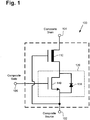
- Figure 1 shows an exemplary implementation of a composite semiconductor device.
- composite semiconductor device 100 includes III-nitride power transistor 110 and LV device 120 cascoded with III-nitride power transistor 110.
- LV device 120 includes LV transistor 140 and LV diode 130.
- composite source 102, composite drain 104, and composite gate 106 of composite semiconductor device 100 are also shown in Figure 1 .
- III-nitride power transistor 110 may be formed of gallium nitride (GaN), and may be implemented as an insulated-gate FET (IGFET) or as a heterostructure FET (HFET), for example.
- III-nitride power transistor 110 may take the form of a metal-insulator-semiconductor FET (MISFET or MISHFET), such as a metal-oxide-semiconductor FET (MOSFET).
- MISFET or MISHFET such as a metal-oxide-semiconductor FET
- MOSFET metal-oxide-semiconductor FET
- III-nitride power transistor 110 when implemented as an HFET, III-nitride power transistor 110 may be a HEMT configured to produce a 2-DEG.
- III-nitride power transistor 110 for example a III-nitride field-effect transistor (III-N FET) or a III-nitride high electron mobility transistor (III-N HEMT), may be a high voltage (HV) device configured to sustain a drain voltage of approximately 600V and having a gate rating of approximately 40V.
- composite semiconductor device 100 may utilize an insulated gate bipolar transistor (IGBT) as a power device in place of a III-nitride FET or HEMT.
- IGBT insulated gate bipolar transistor
- LV device 120 is shown to include LV transistor 140 and LV diode 130.
- LV diode 130 may simply be a body diode of LV transistor 140, while in another implementation LV diode 130 may be a discrete diode coupled to LV transistor 140 as shown in Figure 1 to produce LV device 120.
- LV device 120 may be implemented as an LV group IV device, such as an LV silicon device having a breakdown voltage of approximately 25V, for example.
- LV device 120 may be an LV FET, such as an LV silicon MISFET or MOSFET, for example, including LV body diode 130.
- composite semiconductor device 100 which according to the implementation shown in Figure 1 results in a composite three terminal device functioning in effect as a FET having composite source 102 and composite gate 106 provided by LV device 120, and composite drain 104 provided by III-nitride power transistor 110.
- composite semiconductor device 100 may be implemented as an HV composite device configured to have active oscillation control.
- Figure 2 shows a more detailed implementation of a composite semiconductor device with active oscillation control, corresponding generally to the implementation shown by Figure 1 .
- Composite semiconductor device 200 includes III-nitride power transistor 210, which can be for example a III-N FET or a III-N HEMT, and LV device 220 cascoded with III-nitride power transistor 210.
- LV device 220 includes LV transistor 240 and LV diode 230, which may be a body diode of LV transistor 240, for example.
- FIG. 2 Also shown in Figure 2 are composite source 202, composite drain 204, and composite gate 206 of composite semiconductor device 200, as well as output capacitance 218 (C1) measured across III-nitride power transistor 210, output capacitance 248 (C2) measured across LV device 220 (e.g., LV transistor 240 having LV body diode 230), and semiconductor package inductances 207 (L1) and 209 (L2).
- output capacitance 218 measured across III-nitride power transistor 210
- C2 output capacitance 248
- L1 and 209 L2
- Composite semiconductor device 200 having composite source 202, composite drain 204, composite gate 206, and formed from III-nitride power transistor 210 in combination with LV device 220 including LV transistor 240 and LV diode 230 corresponds to composite semiconductor device 100 having composite source 102, composite drain 104, composite gate 106, and formed from III-nitride power transistor 110 in combination with LV device 120 including LV transistor 140 and LV diode 130, in Figure 1 , and may share any of the features previously attributed to the corresponding components of composite semiconductor device 100 and described above.
- LV transistor 240 is cascoded with III-nitride power transistor 210 to produce composite semiconductor device 200. That is to say, drain 244 of LV transistor 240 is coupled to source 212 of III -nitride power transistor 210, source 242 of LV transistor provides composite source 202 for composite semiconductor device 200, and gate 250 of LV transistor 240 provides composite gate 206 for composite semiconductor device 200. In addition, drain 214 of III-nitride power transistor 210 provides composite drain 204 for composite semiconductor device 200, while gate 216 of III-nitride power transistor 210 is coupled to source 242 of LV transistor 240.
- composite semiconductor device 200 implemented as a normally OFF device formed from LV transistor 240 cascoded with normally ON III-nitride power transistor 210 will now be described by reference to that specific, but merely exemplary, implementation.
- a composite semiconductor device such as composite semiconductor device 200 may be susceptible to oscillations in some high current applications.
- source 212 of III-nitride power transistor 210 may oscillate when configured in series with the circuit including output capacitance 218, semiconductor package inductance 207, and output capacitance 248, (e.g., C1-L1-C2) of Figure 2 .
- Oscillation of source 212 may cause gate 216 of III-nitride power transistor 210 to oscillate as well, which can, in turn, cause normally ON III-nitride power transistor 210 to be switched OFF and ON undesirably. Unless controlled, those oscillations can be destructive.
- the described oscillation phenomenon can be controlled by optimally reducing semiconductor package inductance 207 (L1) and/or 209 (L2).
- semiconductor package inductance 207, and semiconductor package inductance 209 (L2) may be reduced using a die-on-die configuration.
- Specific examples for implementing a die-on-die configuration are disclosed in U.S. Provisional Application No. 61/448,347 entitled “III-Nitride Transistor Stacked with FET in a Package," filed on March 2, 2011, as well as in Provisional Patent Application No. 61/448,617 entitled “III-Nitride Transistor Stacked with Diode in a Package,” filed on March 2, 2011, both of which are hereby incorporated by reference in their entirety.
- semiconductor package inductances 207 and 209 may be reduced through monolithic integration of III-nitride power transistor 210 and LV device 220.
- III-nitride power transistor 210 and LV device 220 may be monolithically integrated as disclosed in U. S. Patent Application Number 12/455,117 , entitled “Monolithic Vertically Integrated Composite Group III-V and Group IV Semiconductor Device and Method for Fabricating Same", filed on May 28, 2009 and issued as U.S. Patent Number 7,915,645 on March 29, 2011 ; as well as by U.S. Patent Application Number 12/653,240 , entitled “Highly Conductive Source/Drain Contacts in III-Nitride Transistors", filed on December 10, 2009; U.S.
- Patent Application Number 12/928,103 entitled “Monolithic Integration of Silicon and Group III-V Devices", filed on December 3, 2010; and U. S. Patent Application Number 13/020,243 entitled “Efficient High Voltage Switching Circuits and Monolithic Integration of Same", filed on February 3, 2011, each of which is hereby incorporated by reference in its entirety.
- undesirable oscillations by composite semiconductor device 200 may be reduced or eliminated through implementation of an active oscillation control, which may be effectuated through configuration of LV transistor 240 to have a reduced output resistance and/or a reduced transconductance due to a modified oxide thickness (T OX ). That is to say, in those applications where composite semiconductor device 200 is designed for high current operation, it may be advantageous to optimize (e.g., limit) the gain (A) of composite semiconductor device 200 from a small signal modeling perspective to less than approximately ten thousand (10,000) in order to provide for stability.
- an active oscillation control which may be effectuated through configuration of LV transistor 240 to have a reduced output resistance and/or a reduced transconductance due to a modified oxide thickness (T OX ). That is to say, in those applications where composite semiconductor device 200 is designed for high current operation, it may be advantageous to optimize (e.g., limit) the gain (A) of composite semiconductor device 200 from a small signal modeling perspective to less than approximately ten thousand (10,000) in order to provide for stability.
- LV transistor 240 can be designed and formed such that one or both of the output resistance of LV transistor 240 and the transconductance partially determined by T OX of LV transistor 240 are optimized so as to limit the gain of composite semiconductor device to a range from approximately 1.0 to less than approximately 10,000, in order to provide active oscillation control for composite semiconductor device 200.
- the expression "oxide thickness" or T OX may refer to the thickness or effective thickness of any suitable gate dielectric utilized to capacitively couple gate 250 of LV transistor 240 to a body region of LV transistor 240 (body region not shown in Figure 2 ).
- T OX may refer to gate dielectrics other than oxides.
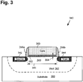
- Figure 3 shows a cross-sectional view of one implementation of LV transistor 340 suitable for use in a composite semiconductor device and configured to provide active oscillation control.
- LV transistor 340 is situated in well 362 formed in substrate 360, and includes source 342, drain 344, and gate 350.
- LV transistor 340 also includes gate dielectric 352 having thickness (e.g., T OX ) 354, spacers 356a and 356b, and body region 346 having body implant 349.
- LV transistor 340 including source 342, drain 344, and gate 350 corresponds to LV transistor 240 including source 242, drain 244, and gate 250, in Figure 2 .
- LV transistor 340 is represented as a FET.
- LV transistor 340 may be fabricated as an n-channel device (NFET) or p-channel device (PFET).
- NFET n-channel device
- PFET p-channel device
- well 362 may be a P type well formed in substrate 360, which may include an epitaxial region formed on a silicon substrate, for example (epitaxial region not distinguished as such in Figure 3 ).
- source 342 and drain 344 may be heavily doped N+ regions, while body region 346 may include a P type body implant 349, such as a boron implant, for example.
- Gate 350 may be formed of a suitable gate metal, or of a doped polysilicon, for example, while gate dielectric 352 may be formed of a gate oxide, such as silicon oxide (SiO 2 ) or, alternatively, a low-k dielectric in various implementations to achieve an increased T OX , as discussed further below.
- Spacers 356a and 356b can be silicon nitride (Si 3 N 4 ) spacers, for example, and can be formed using any suitable technique, as known in the art.
- the gain (A) of composite semiconductor device 200 in Figure 2 , it may be advantageous to reduce the gain (A) of composite semiconductor device 200, in Figure 2 , to less than approximately 10,000 in order to enhance its resistance to undesirable oscillations. That may be achieved through reduction of the transconductance (gm) of composite semiconductor device 200, which includes the transconductance of LV transistor 240 (gm LV ) as well as the transconductance of III-nitride power transistor 210 (gm III-N )
- the gain (A) may be reduced and optimized, such as by being limited to less than approximately 10,000, for example.
- Such a reduction in the gain can be achieved through reduction of one or more of the gain components appearing in Equation 1, i.e., one or more of gm LV, gm III-N , r O-LV, and r O- III-N .
- LV transistor 240 may have a transconductance (gm LV ) in a range from approximately 1.0 mho to approximately 50.0 mhos and an output resistance (r O-LV ) in a range from approximately 0.4 ⁇ to approximately 20.0 ⁇
- III-nitride power transistor 210 may have a transconductance (gm III-N ) in a range from approximately 10.0 mhos to approximately 500.0 mhos and an output resistance (r O-III-N ) in a range from approximately 0.1 ⁇ to approximately 5.0 ⁇ , with the additional constraint that the product: [(gm LV ) * (gm III-N ) * (r O-LV ) * (r O-III-N )] yield a gain of less than 10,000, such as a gain as low as approximately 1.0.
- LV transistor 240 can provide active oscillation control for composite semiconductor device 200 by being configured so as to have a gain limiting (e.g., increased) T OX .
- gate dielectric thickness 354 corresponding to T OX can be increased either in effect, or in fact, to provide active oscillation control for the composite semiconductor device including LV transistor 340.
- An increase in fact of gate dielectric thickness 354 may be accomplished by fabricating LV transistor 340 to have increased gate dielectric thickness 354.
- an increase in effect of gate dielectric thickness 354 may be accomplished by fabricating LV transistor 340 to include a low-k gate dielectric 352, such as, by way of examples and without limitation, porous silica, fluorinated amorphous carbon, aromatic hydrocarbon, carbon-doped oxide, parylene, polyarylene ether, silsesquioxane, fluorinated silicon dioxide, and diamondlike carbon.
- r O-LV can be reduced in order to reduce or eliminate oscillations in the composite semiconductor device including LV transistor 340 by fabricating LV transistor 340 so as to have a gain limiting body implant as body implant 349.
- the energy and dosage of the boron implant used to produce body implant 349 can be modified to reduce the output resistance r O-LV of LV transistor 340.
- an LV device having one or both of a reduced output resistance and a reduced transconductance due to a modified oxide thickness
- cascoding the LV device with a III-nitride power transistor discloses implementations of composite semiconductor devices with active oscillation control.
- an LV group IV device can be advantageously cascoded with a normally ON III-nitride power transistor to produce a rugged, normally OFF HV composite device displaying high durability and stable operation in high current applications.
Landscapes
- Junction Field-Effect Transistors (AREA)
- Metal-Oxide And Bipolar Metal-Oxide Semiconductor Integrated Circuits (AREA)
Abstract
Description
- The present application claims the benefit of and priority to a pending provisional application entitled "III-Nitride Optimized Rugged Cascode Power Device," Serial No.
61/454,743 filed on March 21, 2011 - As used herein, the phrase "III-nitride" or "III-N" refers to a compound semiconductor that includes nitrogen and at least one group III element including aluminum (Al), gallium (Ga), indium (In), and boron (B), and including but not limited to any of its alloys, such as aluminum gallium nitride (AlxGa(1-x)N), indium gallium nitride (InyGa(1-y)N), aluminum indium gallium nitride (AlxInyGa(1-x-y)N), gallium arsenide phosphide nitride (GaAsaPbN(1-a-b)), aluminum indium gallium arsenide phosphide nitride (AlxInyGa(1-x-y)AsaPbN(1-a-b)), for example. III-nitride also refers generally to any polarity including but not limited to Ga-polar, N-polar, semi-polar or non-polar crystal orientations. A III-nitride material may also include either the Wurtzitic, Zincblende or mixed polytypes, and may include single-crystal, monocrystal, polycrystal, or amorphous crystal structures.
- Also, as used herein, the terms "LV-device," "low voltage semiconductor device," "low voltage transistor," and the like, refer to a low voltage device, with a typical voltage range of up to approximately 50 volts. Typical voltage ratings include low voltage (LV) ∼ 0-50V, midvoltage (MV) ∼ 50-200V, high voltage (HV) ∼ 200-1200V and ultra high voltage (UHV) ∼ >1200V. The device can comprise any suitable semiconductor material that forms a field-effect transistor (FET) or diode, or a combination of a FET and a diode. Suitable semiconductor materials include group IV semiconductor materials such as silicon, strained silicon, SiGe, SiC, and group III-V materials including III-As, III-P, III-nitride or any of their alloys.
- III-nitride materials are semiconductor compounds that have a relatively wide, direct bandgap and potentially strong piezoelectric polarizations, and can enable high breakdown fields, high saturation velocities, and the creation of two-dimensional electron gases (2-DEGs). As a result, III-nitride materials are used in many power applications such as depletion mode (e.g., normally ON) power field-effect transistors (power FETs), high electron mobility transistors (HEMTs), and diodes.
- In power management applications where normally OFF characteristics of power devices are desirable, a depletion mode III-nitride power transistor can be cascoded with a low voltage (LV) semiconductor device to produce an enhancement mode composite power device. However, the utility and durability of such a composite device can be limited according to characteristics of the III-nitride power transistor and LV semiconductor device being used in combination. For example, when implemented with an LV semiconductor device to form a composite device used in high current applications, the gate of the III-nitride power transistor may tend to oscillate when configured in series with semiconductor package inductances and the output capacitance of the LV semiconductor device, for example, causing the III-nitride power transistor to be undesirably turned OFF and ON. Unless controlled and dampened, such oscillations may adversely affect the functionality and utility of the composite semiconductor device, and can also be destructive and reduce the durability of the composite semiconductor device.
- The present disclosure is directed to a composite semiconductor device with active oscillation prevention, substantially as shown in and/or described in connection with at least one of the figures, and as set forth more completely in the claims.
-
-
Figure 1 presents a diagram showing one exemplary implementation of a composite semiconductor device. -
Figure 2 shows a more detailed implementation of a composite semiconductor device with active oscillation control, corresponding generally to the implementation shown byFigure 1 . -
Figure 3 shows a cross-sectional view of one implementation of a low voltage (LV) transistor suitable for use in a composite semiconductor device and configured to provide active oscillation control. - The following description contains specific information pertaining to implementations in the present disclosure. One skilled in the art will recognize that the present disclosure may be implemented in a manner different from that specifically discussed herein. The drawings in the present application and their accompanying detailed description are directed to merely exemplary implementations. Unless noted otherwise, like or corresponding elements among the figures may be indicated by like or corresponding reference numerals. Moreover, the drawings and illustrations in the present application are generally not to scale, and are not intended to correspond to actual relative dimensions.
- III-nitride materials include, for example, gallium nitride (GaN) and its alloys such as aluminum gallium nitride (AlGaN), indium gallium nitride (InGaN), and aluminum indium gallium nitride (AlInGaN). These materials are semiconductor compounds that have a relatively wide, direct bandgap and strong piezoelectric polarizations, and can enable high breakdown fields, high saturation velocities, and the creation of two-dimensional electron gases (2-DEGs). As a result, and as noted above, III-nitride materials such as GaN are used in many microelectronic applications such as depletion mode (e.g., normally ON) power field-effect transistors (power FETs), high electron mobility transistors (HEMTs), and diodes.
- As further noted above, in power management applications where normally OFF characteristics of power devices are desirable, a depletion mode III-nitride power transistor can be cascoded with a low voltage (LV) semiconductor device to produce an enhancement mode composite power device. However, the utility and durability of such a composite device can be limited according to characteristics of the III-nitride power transistor and LV semiconductor device being cascoded together. For example, when implemented in combination with an LV semiconductor device to form a composite device used in high current applications, the gate of the III-nitride power transistor may tend to oscillate when configured in series with semiconductor package inductances and the output capacitance of the LV semiconductor device, for example, causing the III-nitride power transistor to be turned OFF and ON. Unless controlled, such oscillations can be destructive, and may undesirably reduce the durability of the composite semiconductor device. Thus, in order to render such composite semiconductor devices suitable for operation in power management systems, where high slew rate conditions may be encountered, the composite device should be configured so as to be oscillation resistant.
- The present application is directed to a composite semiconductor device with active oscillation control. According to one implementation, the composite semiconductor device may include a III-nitride power transistor, which may be a normally ON device, for example, and an LV device cascoded with the III-nitride power transistor. \The cascoded combination of the LV device and the normally ON III-nitride power transistor can be implemented to produce a normally OFF composite semiconductor device. As disclosed herein, the LV device cascoded with the normally ON III-nitride power transistor can be configured so as to limit the gain of the composite semiconductor device to provide active oscillation control for the normally OFF composite semiconductor device.
- Referring to
Figure 1, Figure 1 shows an exemplary implementation of a composite semiconductor device. As shown inFigure 1 ,composite semiconductor device 100 includes III-nitride power transistor 110 andLV device 120 cascoded with III-nitride power transistor 110. As further shown inFigure 1 ,LV device 120 includesLV transistor 140 andLV diode 130. Also shown inFigure 1 arecomposite source 102,composite drain 104, andcomposite gate 106 ofcomposite semiconductor device 100. - III-
nitride power transistor 110 may be formed of gallium nitride (GaN), and may be implemented as an insulated-gate FET (IGFET) or as a heterostructure FET (HFET), for example. In one implementation, III-nitride power transistor 110 may take the form of a metal-insulator-semiconductor FET (MISFET or MISHFET), such as a metal-oxide-semiconductor FET (MOSFET). Alternatively, when implemented as an HFET, III-nitride power transistor 110 may be a HEMT configured to produce a 2-DEG. According to one implementation, for example, III-nitride power transistor 110, for example a III-nitride field-effect transistor (III-N FET) or a III-nitride high electron mobility transistor (III-N HEMT), may be a high voltage (HV) device configured to sustain a drain voltage of approximately 600V and having a gate rating of approximately 40V. It is noted that in some implementations,composite semiconductor device 100 may utilize an insulated gate bipolar transistor (IGBT) as a power device in place of a III-nitride FET or HEMT. -
LV device 120 is shown to includeLV transistor 140 andLV diode 130. In one implementation,LV diode 130 may simply be a body diode ofLV transistor 140, while in anotherimplementation LV diode 130 may be a discrete diode coupled toLV transistor 140 as shown inFigure 1 to produceLV device 120.LV device 120 may be implemented as an LV group IV device, such as an LV silicon device having a breakdown voltage of approximately 25V, for example. According to one implementation,LV device 120 may be an LV FET, such as an LV silicon MISFET or MOSFET, for example, includingLV body diode 130. - The cascoded combination of III-
nitride power transistor 110 andLV device 120 producescomposite semiconductor device 100, which according to the implementation shown inFigure 1 results in a composite three terminal device functioning in effect as a FET havingcomposite source 102 andcomposite gate 106 provided byLV device 120, andcomposite drain 104 provided by III-nitride power transistor 110. Moreover, and as will be described in greater detail below,composite semiconductor device 100 may be implemented as an HV composite device configured to have active oscillation control. - Continuing to
Figure 2, Figure 2 shows a more detailed implementation of a composite semiconductor device with active oscillation control, corresponding generally to the implementation shown byFigure 1 .Composite semiconductor device 200 includes III-nitride power transistor 210, which can be for example a III-N FET or a III-N HEMT, andLV device 220 cascoded with III-nitride power transistor 210. As further shown inFigure 2 ,LV device 220 includesLV transistor 240 andLV diode 230, which may be a body diode ofLV transistor 240, for example. Also shown inFigure 2 arecomposite source 202,composite drain 204, andcomposite gate 206 ofcomposite semiconductor device 200, as well as output capacitance 218 (C1) measured across III-nitride power transistor 210, output capacitance 248 (C2) measured across LV device 220 (e.g.,LV transistor 240 having LV body diode 230), and semiconductor package inductances 207 (L1) and 209 (L2). -
Composite semiconductor device 200 havingcomposite source 202,composite drain 204,composite gate 206, and formed from III-nitride power transistor 210 in combination withLV device 220 includingLV transistor 240 andLV diode 230 corresponds tocomposite semiconductor device 100 havingcomposite source 102,composite drain 104,composite gate 106, and formed from III-nitride power transistor 110 in combination withLV device 120 includingLV transistor 140 andLV diode 130, inFigure 1 , and may share any of the features previously attributed to the corresponding components ofcomposite semiconductor device 100 and described above. - As shown in
Figure 2 ,LV transistor 240 is cascoded with III-nitride power transistor 210 to producecomposite semiconductor device 200. That is to say,drain 244 ofLV transistor 240 is coupled tosource 212 of III-nitride power transistor 210,source 242 of LV transistor providescomposite source 202 forcomposite semiconductor device 200, andgate 250 ofLV transistor 240 providescomposite gate 206 forcomposite semiconductor device 200. In addition, drain 214 of III-nitride power transistor 210 providescomposite drain 204 forcomposite semiconductor device 200, whilegate 216 of III-nitride power transistor 210 is coupled tosource 242 ofLV transistor 240. - The operation of
composite semiconductor device 200 implemented as a normally OFF device formed fromLV transistor 240 cascoded with normally ON III-nitride power transistor 210 will now be described by reference to that specific, but merely exemplary, implementation. As previously noted above, in the absence of the active oscillation control disclosed herein, a composite semiconductor device such ascomposite semiconductor device 200 may be susceptible to oscillations in some high current applications. During high slew rate conditions, for example,source 212 of III-nitride power transistor 210 may oscillate when configured in series with the circuit includingoutput capacitance 218,semiconductor package inductance 207, andoutput capacitance 248, (e.g., C1-L1-C2) ofFigure 2 . Oscillation ofsource 212 may causegate 216 of III-nitride power transistor 210 to oscillate as well, which can, in turn, cause normally ON III-nitride power transistor 210 to be switched OFF and ON undesirably. Unless controlled, those oscillations can be destructive. - In some implementations, the described oscillation phenomenon can be controlled by optimally reducing semiconductor package inductance 207 (L1) and/or 209 (L2). In one implementation, for instance,
semiconductor package inductance 207, and semiconductor package inductance 209 (L2), may be reduced using a die-on-die configuration. Specific examples for implementing a die-on-die configuration are disclosed inU.S. Provisional Application No. 61/448,347 61/448,617 - According to another implementation,
semiconductor package inductances nitride power transistor 210 andLV device 220. For example, III-nitride power transistor 210 andLV device 220 may be monolithically integrated as disclosed inU. S. Patent Application Number 12/455,117 U.S. Patent Number 7,915,645 on March 29, 2011 ; as well as byU.S. Patent Application Number 12/653,240 U.S. Patent Application Number 12/928,103 U. S. Patent Application Number 13/020,243 entitled "Efficient High Voltage Switching Circuits and Monolithic Integration of Same", filed on February 3, 2011, each of which is hereby incorporated by reference in its entirety. - Alternatively, and as disclosed herein, undesirable oscillations by
composite semiconductor device 200 may be reduced or eliminated through implementation of an active oscillation control, which may be effectuated through configuration ofLV transistor 240 to have a reduced output resistance and/or a reduced transconductance due to a modified oxide thickness (TOX). That is to say, in those applications wherecomposite semiconductor device 200 is designed for high current operation, it may be advantageous to optimize (e.g., limit) the gain (A) ofcomposite semiconductor device 200 from a small signal modeling perspective to less than approximately ten thousand (10,000) in order to provide for stability. For example,LV transistor 240 can be designed and formed such that one or both of the output resistance ofLV transistor 240 and the transconductance partially determined by TOX ofLV transistor 240 are optimized so as to limit the gain of composite semiconductor device to a range from approximately 1.0 to less than approximately 10,000, in order to provide active oscillation control forcomposite semiconductor device 200. It is noted that, more generally, the expression "oxide thickness" or TOX may refer to the thickness or effective thickness of any suitable gate dielectric utilized to capacitivelycouple gate 250 ofLV transistor 240 to a body region of LV transistor 240 (body region not shown inFigure 2 ). Thus, as used herein, TOX may refer to gate dielectrics other than oxides. - Referring now to
Figure 3, Figure 3 shows a cross-sectional view of one implementation ofLV transistor 340 suitable for use in a composite semiconductor device and configured to provide active oscillation control. As shown inFigure 3 ,LV transistor 340 is situated in well 362 formed insubstrate 360, and includessource 342, drain 344, andgate 350. As further shown inFigure 3 ,LV transistor 340 also includes gate dielectric 352 having thickness (e.g., TOX) 354,spacers body region 346 havingbody implant 349.LV transistor 340 includingsource 342, drain 344, andgate 350 corresponds toLV transistor 240 includingsource 242, drain 244, andgate 250, inFigure 2 . - According to the implementation shown in
Figure 3 ,LV transistor 340 is represented as a FET. When implemented as such,LV transistor 340 may be fabricated as an n-channel device (NFET) or p-channel device (PFET). Although for the purposes of the presentdiscussion LV device 340 will be described as an NFET, that example characterization is not to be interpreted as a limitation. - When
LV transistor 340 is implemented as an NFET, well 362 may be a P type well formed insubstrate 360, which may include an epitaxial region formed on a silicon substrate, for example (epitaxial region not distinguished as such inFigure 3 ). Moreover, in such an implementation,source 342 and drain 344 may be heavily doped N+ regions, whilebody region 346 may include a Ptype body implant 349, such as a boron implant, for example.Gate 350 may be formed of a suitable gate metal, or of a doped polysilicon, for example, whilegate dielectric 352 may be formed of a gate oxide, such as silicon oxide (SiO2) or, alternatively, a low-k dielectric in various implementations to achieve an increased TOX, as discussed further below.Spacers - As discussed above, it may be advantageous to reduce the gain (A) of
composite semiconductor device 200, inFigure 2 , to less than approximately 10,000 in order to enhance its resistance to undesirable oscillations. That may be achieved through reduction of the transconductance (gm) ofcomposite semiconductor device 200, which includes the transconductance of LV transistor 240 (gmLV) as well as the transconductance of III-nitride power transistor 210 (gmIII-N) For example, the small signal gain ofcomposite semiconductor 200 may be described by Equation 1:
where rO-LV is the output resistance ofLV transistor 240 and ro- III-N is the output resistance of III-nitride power transistor 210. - In order to reduce or eliminate oscillations and render
composite semiconductor device 200 substantially stable, the gain (A) may be reduced and optimized, such as by being limited to less than approximately 10,000, for example. Such a reduction in the gain can be achieved through reduction of one or more of the gain components appearing inEquation 1, i.e., one or more of gmLV, gmIII-N, rO-LV, and rO- III-N. For example,LV transistor 240 may have a transconductance (gmLV) in a range from approximately 1.0 mho to approximately 50.0 mhos and an output resistance (rO-LV) in a range from approximately 0.4 Ω to approximately 20.0 Ω, while III-nitride power transistor 210 may have a transconductance (gmIII-N) in a range from approximately 10.0 mhos to approximately 500.0 mhos and an output resistance (rO-III-N) in a range from approximately 0.1 Ω to approximately 5.0 Ω, with the additional constraint that the product: [(gmLV) * (gmIII-N) * (rO-LV) * (rO-III-N)] yield a gain of less than 10,000, such as a gain as low as approximately 1.0. - With respect to gmLV, the proportionality relationship of gmLV to TOX is described by Equation 2:

Thus, modifying the oxide thickness by increasing TOX decreases gmLV and consequently the gain (A) ofcomposite semiconductor device 200. As a result,LV transistor 240 can provide active oscillation control forcomposite semiconductor device 200 by being configured so as to have a gain limiting (e.g., increased) TOX. - Referring to
Figure 3 ,gate dielectric thickness 354 corresponding to TOX can be increased either in effect, or in fact, to provide active oscillation control for the composite semiconductor device includingLV transistor 340. An increase in fact ofgate dielectric thickness 354 may be accomplished by fabricatingLV transistor 340 to have increasedgate dielectric thickness 354. Alternatively, an increase in effect ofgate dielectric thickness 354 may be accomplished by fabricatingLV transistor 340 to include a low-k gate dielectric 352, such as, by way of examples and without limitation, porous silica, fluorinated amorphous carbon, aromatic hydrocarbon, carbon-doped oxide, parylene, polyarylene ether, silsesquioxane, fluorinated silicon dioxide, and diamondlike carbon. - Referring once again to
Equation 1, another possible gain limiting component is the output resistance ofLV transistor 340, i.e., rO-LV As may be understood, rO-LV can be reduced in order to reduce or eliminate oscillations in the composite semiconductor device includingLV transistor 340 by fabricatingLV transistor 340 so as to have a gain limiting body implant asbody implant 349. For example, in the described exemplary NFET implementation, the energy and dosage of the boron implant used to producebody implant 349 can be modified to reduce the output resistance rO-LV ofLV transistor 340. - Thus, by utilizing an LV device having one or both of a reduced output resistance and a reduced transconductance due to a modified oxide thickness, and cascoding the LV device with a III-nitride power transistor, the present application discloses implementations of composite semiconductor devices with active oscillation control. As a result, an LV group IV device can be advantageously cascoded with a normally ON III-nitride power transistor to produce a rugged, normally OFF HV composite device displaying high durability and stable operation in high current applications.
- From the above description it is manifest that various techniques can be used for implementing the concepts described in the present application without departing from the scope of those concepts. Moreover, while the concepts have been described with specific reference to certain implementations, a person of ordinary skill in the art would recognize that changes can be made in form and detail without departing from the spirit and the scope of those concepts. As such, the described implementations are to be considered in all respects as illustrative and not restrictive. It should also be understood that the present application is not limited to the particular implementations described herein, but many rearrangements, modifications, and substitutions are possible without departing from the scope of the present disclosure.
Claims (15)
- A normally OFF composite semiconductor device including an active oscillation control, said normally OFF composite semiconductor device comprising:a normally ON III-nitride power transistor;a low voltage (LV) device cascoded with said normally ON III-nitride power transistor to form said normally OFF composite semiconductor device;said LV device having a reduced output resistance to cause a gain of said normally OFF composite semiconductor device to be less than approximately 10,000.
- The normally OFF composite semiconductor device of claim 1, wherein said normally ON III-nitride power transistor comprises a III-nitride field-effect transistor (III-N FET).
- The normally OFF composite semiconductor device of claim 1, wherein said normally ON III-nitride power transistor comprises a III-nitride high electron mobility transistor (III-N HEMT).
- The normally OFF composite semiconductor device of claim 1, wherein said LV device comprises an LV group IV semiconductor device.
- The normally OFF composite semiconductor device of claim 1, wherein said normally ON III-nitride power transistor and said LV device are monolithically integrated.
- A composite semiconductor device including an active oscillation control, said composite semiconductor device comprising:a III-nitride power transistor;a low voltage (LV) transistor;a drain of said LV transistor coupled to a source said III-nitride power transistor, a source of said LV transistor providing a composite source for said composite semiconductor device, and a gate of said LV transistor providing a composite gate for said composite semiconductor device, a drain of said III-nitride power transistor providing a composite drain for said composite semiconductor device, a gate of said III-nitride power transistor being coupled to said source of said LV transistor;said LV transistor having a reduced output resistance due to a modified body implant to cause a gain of said composite semiconductor device to be less than approximately 10,000.
- The composite semiconductor device of claim 6, wherein said III-nitride power transistor comprises a III-nitride field-effect transistor (III-N FET).
- The composite semiconductor device of claim 6, wherein said III-nitride power transistor comprises a III-nitride high electron mobility transistor (III-N HEMT).
- The composite semiconductor device of claim 6, wherein said LV transistor comprises an LV group IV semiconductor transistor.
- The composite semiconductor device of claim 6, wherein said LV transistor comprises an LV silicon field-effect transistor (FET).
- The composite semiconductor device of claim 6, wherein said III-nitride power transistor and said LV transistor are monolithically integrated.
- A composite semiconductor device including an active oscillation control, said composite semiconductor device comprising:a III-nitride power transistor;a low voltage (LV) transistor;a drain of said LV transistor coupled to a source said III-nitride power transistor, a source of said LV transistor providing a composite source for said composite semiconductor device, and a gate of said LV transistor providing a composite gate for said composite semiconductor device, a drain of said III-nitride power transistor providing a composite drain for said composite semiconductor device, a gate of said III-nitride power transistor being coupled to said source of said LV transistor;said LV transistor having a reduced transconductance due to a modified oxide thickness to cause a gain of said composite semiconductor device to be less than approximately 10,000.
- The composite semiconductor device of claim 12, wherein said III-nitride power transistor comprises a III-nitride field-effect transistor (III-N FET).
- The composite semiconductor device of claim 12, wherein said III-nitride power transistor comprises a III-nitride high electron mobility transistor (III-N HEMT).
- The composite semiconductor device of claim 12, wherein said LV transistor comprises an LV silicon field-effect transistor (FET).
Applications Claiming Priority (2)
| Application Number | Priority Date | Filing Date | Title |
|---|---|---|---|
| US201161454743P | 2011-03-21 | 2011-03-21 | |
| US13/417,143 US8766375B2 (en) | 2011-03-21 | 2012-03-09 | Composite semiconductor device with active oscillation prevention |
Publications (2)
| Publication Number | Publication Date |
|---|---|
| EP2503693A1 true EP2503693A1 (en) | 2012-09-26 |
| EP2503693B1 EP2503693B1 (en) | 2013-11-20 |
Family
ID=45841348
Family Applications (1)
| Application Number | Title | Priority Date | Filing Date |
|---|---|---|---|
| EP12159776.9A Active EP2503693B1 (en) | 2011-03-21 | 2012-03-15 | Composite Semiconductor Device with Active Oscillation Prevention |
Country Status (3)
| Country | Link |
|---|---|
| US (1) | US8766375B2 (en) |
| EP (1) | EP2503693B1 (en) |
| JP (1) | JP5848171B2 (en) |
Cited By (2)
| Publication number | Priority date | Publication date | Assignee | Title |
|---|---|---|---|---|
| US9762232B2 (en) | 2013-12-27 | 2017-09-12 | Fujitsu Limited | Semiconductor device |
| US10446675B2 (en) | 2017-08-23 | 2019-10-15 | X-Fab Semiconductor Foundries Ag | Noff III-nitride high electron mobility transistor |
Families Citing this family (17)
| Publication number | Priority date | Publication date | Assignee | Title |
|---|---|---|---|---|
| US9859882B2 (en) | 2011-03-21 | 2018-01-02 | Infineon Technologies Americas Corp. | High voltage composite semiconductor device with protection for a low voltage device |
| US9236376B2 (en) | 2011-03-21 | 2016-01-12 | Infineon Technologies Americas Corp. | Power semiconductor device with oscillation prevention |
| US9362905B2 (en) | 2011-03-21 | 2016-06-07 | Infineon Technologies Americas Corp. | Composite semiconductor device with turn-on prevention control |
| JP2013153027A (en) * | 2012-01-24 | 2013-08-08 | Fujitsu Ltd | Semiconductor device and power supply device |
| KR101922117B1 (en) * | 2012-08-16 | 2018-11-26 | 삼성전자주식회사 | Electronic device including transistor and method of operating the same |
| JP6048026B2 (en) * | 2012-09-20 | 2016-12-21 | 富士通株式会社 | Power supply circuit and power supply device |
| JP6113542B2 (en) * | 2013-03-21 | 2017-04-12 | 株式会社東芝 | Semiconductor device |
| US9007117B2 (en) * | 2013-08-02 | 2015-04-14 | Infineon Technologies Dresden Gmbh | Solid-state switching device having a high-voltage switching transistor and a low-voltage driver transistor |
| JP2015056457A (en) * | 2013-09-10 | 2015-03-23 | 株式会社東芝 | Semiconductor device |
| US20150162321A1 (en) | 2013-12-09 | 2015-06-11 | International Rectifier Corporation | Composite Power Device with ESD Protection Clamp |
| US9331204B2 (en) | 2014-03-13 | 2016-05-03 | Macronix International Co., Ltd. | High voltage field effect transistors and circuits utilizing the same |
| JP6203097B2 (en) * | 2014-03-20 | 2017-09-27 | 株式会社東芝 | Semiconductor device |
| CN103887961B (en) * | 2014-04-18 | 2015-06-10 | 杭州士兰微电子股份有限公司 | Switching power supply and controller thereof |
| JP6509621B2 (en) * | 2015-04-22 | 2019-05-08 | ルネサスエレクトロニクス株式会社 | Semiconductor device |
| US9837399B2 (en) * | 2015-07-24 | 2017-12-05 | Semiconductor Components Industries, Llc | Cascode configured semiconductor component and method |
| CN107925404A (en) * | 2015-09-10 | 2018-04-17 | 古河电气工业株式会社 | power component |
| JP7017016B2 (en) * | 2017-03-07 | 2022-02-08 | 学校法人早稲田大学 | Normal off operation diamond power device and inverter using it |
Citations (3)
| Publication number | Priority date | Publication date | Assignee | Title |
|---|---|---|---|---|
| US20070210333A1 (en) * | 2006-03-10 | 2007-09-13 | International Rectifier Corp. | Hybrid semiconductor device |
| EP2242103A1 (en) * | 2009-03-24 | 2010-10-20 | ViaSat, Inc. | Chip with field-effect transistors and contact bumps for flip-chip connection |
| US7915645B2 (en) | 2009-05-28 | 2011-03-29 | International Rectifier Corporation | Monolithic vertically integrated composite group III-V and group IV semiconductor device and method for fabricating same |
Family Cites Families (34)
| Publication number | Priority date | Publication date | Assignee | Title |
|---|---|---|---|---|
| US4663547A (en) | 1981-04-24 | 1987-05-05 | General Electric Company | Composite circuit for power semiconductor switching |
| JPH03196572A (en) | 1989-12-25 | 1991-08-28 | Mitsubishi Electric Corp | Semiconductor device |
| US5142239A (en) * | 1991-05-20 | 1992-08-25 | Motorola, Inc. | High frequency linear amplifier assembly |
| JPH07146722A (en) * | 1993-10-01 | 1995-06-06 | Fuji Electric Co Ltd | Overcurrent protection device for transistor |
| JPH08308092A (en) | 1995-04-27 | 1996-11-22 | Sony Tektronix Corp | Highly voltage-resistant circuit breaker apparatus |
| JP3196572B2 (en) | 1995-05-29 | 2001-08-06 | 松下電器産業株式会社 | Electric water heater |
| US5939753A (en) | 1997-04-02 | 1999-08-17 | Motorola, Inc. | Monolithic RF mixed signal IC with power amplification |
| DE19943785A1 (en) | 1998-09-25 | 2000-03-30 | Siemens Ag | Electronic cascade circuit, e.g. with a silicon MOSFET and a silicon carbide JFET, has a first component grid control voltage partially applied to a second component grid connection at a level below its p-n junction diffusion voltage |
| US6316809B1 (en) * | 1999-01-06 | 2001-11-13 | Lucent Technologies Inc. | Analog MOSFET devices |
| JP4751002B2 (en) | 2001-07-11 | 2011-08-17 | 富士通株式会社 | Cascode type distributed amplifier |
| US7202528B2 (en) | 2004-12-01 | 2007-04-10 | Semisouth Laboratories, Inc. | Normally-off integrated JFET power switches in wide bandgap semiconductors and methods of making |
| JP2006086398A (en) | 2004-09-17 | 2006-03-30 | Matsushita Electric Ind Co Ltd | Semiconductor device and manufacturing method thereof |
| JP2006223016A (en) | 2005-02-08 | 2006-08-24 | Renesas Technology Corp | Power system, multi-chip module, system-in-package, and non-isolated DC / DC converter |
| JP4645313B2 (en) | 2005-06-14 | 2011-03-09 | 富士電機システムズ株式会社 | Semiconductor device |
| JP4821214B2 (en) | 2005-08-26 | 2011-11-24 | 三菱電機株式会社 | Cascode connection circuit |
| US20070170897A1 (en) | 2006-01-26 | 2007-07-26 | Advanced Analogic Technologies, Inc. | High-Frequency Power MESFET Buck Switching Power Supply |
| WO2007109301A2 (en) | 2006-03-20 | 2007-09-27 | International Rectifier Corporation | Merged gate cascode transistor |
| JP2007273640A (en) | 2006-03-30 | 2007-10-18 | Sanken Electric Co Ltd | Semiconductor device |
| JP5358882B2 (en) | 2007-02-09 | 2013-12-04 | サンケン電気株式会社 | Composite semiconductor device including rectifying element |
| US7501670B2 (en) | 2007-03-20 | 2009-03-10 | Velox Semiconductor Corporation | Cascode circuit employing a depletion-mode, GaN-based FET |
| JP5386785B2 (en) | 2007-03-26 | 2014-01-15 | サンケン電気株式会社 | Semiconductor device and manufacturing method thereof |
| US7719055B1 (en) | 2007-05-10 | 2010-05-18 | Northrop Grumman Systems Corporation | Cascode power switch topologies |
| JP2008306130A (en) | 2007-06-11 | 2008-12-18 | Sanken Electric Co Ltd | Field effect semiconductor device and method for manufacturing the same |
| JP2009038130A (en) | 2007-07-31 | 2009-02-19 | Mitsumi Electric Co Ltd | Horizontal MOS transistor and semiconductor device using the same |
| JP2010094006A (en) | 2008-09-10 | 2010-04-22 | Panasonic Corp | Gate drive circuit and inverter circuit using the same |
| JP4911158B2 (en) * | 2008-10-30 | 2012-04-04 | ソニー株式会社 | Semiconductor device and solid-state imaging device |
| US8084783B2 (en) | 2008-11-10 | 2011-12-27 | International Rectifier Corporation | GaN-based device cascoded with an integrated FET/Schottky diode device |
| DE102009005120B4 (en) | 2009-01-19 | 2014-08-07 | Intel Mobile Communications GmbH | Electronic circuit and electronic circuit arrangement |
| CH700697A2 (en) | 2009-03-27 | 2010-09-30 | Eth Zuerich | SWITCHING DEVICE WITH A cascade circuit. |
| JP2010278280A (en) | 2009-05-29 | 2010-12-09 | Toshiba Corp | High frequency semiconductor device |
| JP2011029386A (en) | 2009-07-24 | 2011-02-10 | Sharp Corp | Semiconductor device and electronic apparatus |
| US9378965B2 (en) | 2009-12-10 | 2016-06-28 | Infineon Technologies Americas Corp. | Highly conductive source/drain contacts in III-nitride transistors |
| US8981380B2 (en) | 2010-03-01 | 2015-03-17 | International Rectifier Corporation | Monolithic integration of silicon and group III-V devices |
| JP5653326B2 (en) | 2011-09-12 | 2015-01-14 | 株式会社東芝 | Nitride semiconductor device |
-
2012
- 2012-03-09 US US13/417,143 patent/US8766375B2/en active Active
- 2012-03-15 JP JP2012059460A patent/JP5848171B2/en active Active
- 2012-03-15 EP EP12159776.9A patent/EP2503693B1/en active Active
Patent Citations (3)
| Publication number | Priority date | Publication date | Assignee | Title |
|---|---|---|---|---|
| US20070210333A1 (en) * | 2006-03-10 | 2007-09-13 | International Rectifier Corp. | Hybrid semiconductor device |
| EP2242103A1 (en) * | 2009-03-24 | 2010-10-20 | ViaSat, Inc. | Chip with field-effect transistors and contact bumps for flip-chip connection |
| US7915645B2 (en) | 2009-05-28 | 2011-03-29 | International Rectifier Corporation | Monolithic vertically integrated composite group III-V and group IV semiconductor device and method for fabricating same |
Cited By (2)
| Publication number | Priority date | Publication date | Assignee | Title |
|---|---|---|---|---|
| US9762232B2 (en) | 2013-12-27 | 2017-09-12 | Fujitsu Limited | Semiconductor device |
| US10446675B2 (en) | 2017-08-23 | 2019-10-15 | X-Fab Semiconductor Foundries Ag | Noff III-nitride high electron mobility transistor |
Also Published As
| Publication number | Publication date |
|---|---|
| JP2012199547A (en) | 2012-10-18 |
| EP2503693B1 (en) | 2013-11-20 |
| US8766375B2 (en) | 2014-07-01 |
| US20130234208A1 (en) | 2013-09-12 |
| JP5848171B2 (en) | 2016-01-27 |
Similar Documents
| Publication | Publication Date | Title |
|---|---|---|
| EP2503693B1 (en) | Composite Semiconductor Device with Active Oscillation Prevention | |
| US9859882B2 (en) | High voltage composite semiconductor device with protection for a low voltage device | |
| US9397089B2 (en) | Group III-V HEMT having a selectably floating substrate | |
| EP3696980B1 (en) | Configurations of composite devices comprising of a normally-on fet and a normally-off fet | |
| EP2503694A2 (en) | III-nitride transistor with passive oscillation prevention | |
| CN103000682B (en) | Nitride compound semiconductor device | |
| US11631741B2 (en) | Semiconductor device | |
| US20150162321A1 (en) | Composite Power Device with ESD Protection Clamp | |
| EP2503692B1 (en) | Composite Semiconductor Device with Higher Threshold Voltage | |
| US8988133B2 (en) | Nested composite switch | |
| US20140225163A1 (en) | Inverter Circuit Including Short Circuit Protected Composite Switch | |
| EP2546986A2 (en) | Nested Composite Diode | |
| US20160248422A1 (en) | Switching circuit, semiconductor switching arrangement and method | |
| US11355625B2 (en) | Device and semiconductor structure for improving the disadvantages of p-GaN gate high electron mobility transistor | |
| US9236376B2 (en) | Power semiconductor device with oscillation prevention |
Legal Events
| Date | Code | Title | Description |
|---|---|---|---|
| PUAI | Public reference made under article 153(3) epc to a published international application that has entered the european phase |
Free format text: ORIGINAL CODE: 0009012 |
|
| AK | Designated contracting states |
Kind code of ref document: A1 Designated state(s): AL AT BE BG CH CY CZ DE DK EE ES FI FR GB GR HR HU IE IS IT LI LT LU LV MC MK MT NL NO PL PT RO RS SE SI SK SM TR |
|
| AX | Request for extension of the european patent |
Extension state: BA ME |
|
| 17P | Request for examination filed |
Effective date: 20130326 |
|
| GRAP | Despatch of communication of intention to grant a patent |
Free format text: ORIGINAL CODE: EPIDOSNIGR1 |
|
| INTG | Intention to grant announced |
Effective date: 20130904 |
|
| GRAS | Grant fee paid |
Free format text: ORIGINAL CODE: EPIDOSNIGR3 |
|
| GRAA | (expected) grant |
Free format text: ORIGINAL CODE: 0009210 |
|
| AK | Designated contracting states |
Kind code of ref document: B1 Designated state(s): AL AT BE BG CH CY CZ DE DK EE ES FI FR GB GR HR HU IE IS IT LI LT LU LV MC MK MT NL NO PL PT RO RS SE SI SK SM TR |
|
| REG | Reference to a national code |
Ref country code: GB Ref legal event code: FG4D |
|
| REG | Reference to a national code |
Ref country code: CH Ref legal event code: EP |
|
| REG | Reference to a national code |
Ref country code: AT Ref legal event code: REF Ref document number: 642146 Country of ref document: AT Kind code of ref document: T Effective date: 20131215 |
|
| REG | Reference to a national code |
Ref country code: IE Ref legal event code: FG4D |
|
| REG | Reference to a national code |
Ref country code: DE Ref legal event code: R096 Ref document number: 602012000529 Country of ref document: DE Effective date: 20140116 |
|
| REG | Reference to a national code |
Ref country code: NL Ref legal event code: VDEP Effective date: 20131120 |
|
| REG | Reference to a national code |
Ref country code: AT Ref legal event code: MK05 Ref document number: 642146 Country of ref document: AT Kind code of ref document: T Effective date: 20131120 |
|
| REG | Reference to a national code |
Ref country code: LT Ref legal event code: MG4D |
|
| PG25 | Lapsed in a contracting state [announced via postgrant information from national office to epo] |
Ref country code: FI Free format text: LAPSE BECAUSE OF FAILURE TO SUBMIT A TRANSLATION OF THE DESCRIPTION OR TO PAY THE FEE WITHIN THE PRESCRIBED TIME-LIMIT Effective date: 20131120 Ref country code: IS Free format text: LAPSE BECAUSE OF FAILURE TO SUBMIT A TRANSLATION OF THE DESCRIPTION OR TO PAY THE FEE WITHIN THE PRESCRIBED TIME-LIMIT Effective date: 20140320 Ref country code: SE Free format text: LAPSE BECAUSE OF FAILURE TO SUBMIT A TRANSLATION OF THE DESCRIPTION OR TO PAY THE FEE WITHIN THE PRESCRIBED TIME-LIMIT Effective date: 20131120 Ref country code: HR Free format text: LAPSE BECAUSE OF FAILURE TO SUBMIT A TRANSLATION OF THE DESCRIPTION OR TO PAY THE FEE WITHIN THE PRESCRIBED TIME-LIMIT Effective date: 20131120 Ref country code: LT Free format text: LAPSE BECAUSE OF FAILURE TO SUBMIT A TRANSLATION OF THE DESCRIPTION OR TO PAY THE FEE WITHIN THE PRESCRIBED TIME-LIMIT Effective date: 20131120 Ref country code: NL Free format text: LAPSE BECAUSE OF FAILURE TO SUBMIT A TRANSLATION OF THE DESCRIPTION OR TO PAY THE FEE WITHIN THE PRESCRIBED TIME-LIMIT Effective date: 20131120 Ref country code: NO Free format text: LAPSE BECAUSE OF FAILURE TO SUBMIT A TRANSLATION OF THE DESCRIPTION OR TO PAY THE FEE WITHIN THE PRESCRIBED TIME-LIMIT Effective date: 20140220 |
|
| PG25 | Lapsed in a contracting state [announced via postgrant information from national office to epo] |
Ref country code: RS Free format text: LAPSE BECAUSE OF FAILURE TO SUBMIT A TRANSLATION OF THE DESCRIPTION OR TO PAY THE FEE WITHIN THE PRESCRIBED TIME-LIMIT Effective date: 20131120 Ref country code: LV Free format text: LAPSE BECAUSE OF FAILURE TO SUBMIT A TRANSLATION OF THE DESCRIPTION OR TO PAY THE FEE WITHIN THE PRESCRIBED TIME-LIMIT Effective date: 20131120 Ref country code: AT Free format text: LAPSE BECAUSE OF FAILURE TO SUBMIT A TRANSLATION OF THE DESCRIPTION OR TO PAY THE FEE WITHIN THE PRESCRIBED TIME-LIMIT Effective date: 20131120 Ref country code: ES Free format text: LAPSE BECAUSE OF FAILURE TO SUBMIT A TRANSLATION OF THE DESCRIPTION OR TO PAY THE FEE WITHIN THE PRESCRIBED TIME-LIMIT Effective date: 20131120 Ref country code: BE Free format text: LAPSE BECAUSE OF FAILURE TO SUBMIT A TRANSLATION OF THE DESCRIPTION OR TO PAY THE FEE WITHIN THE PRESCRIBED TIME-LIMIT Effective date: 20131120 |
|
| PG25 | Lapsed in a contracting state [announced via postgrant information from national office to epo] |
Ref country code: PT Free format text: LAPSE BECAUSE OF FAILURE TO SUBMIT A TRANSLATION OF THE DESCRIPTION OR TO PAY THE FEE WITHIN THE PRESCRIBED TIME-LIMIT Effective date: 20140320 |
|
| PG25 | Lapsed in a contracting state [announced via postgrant information from national office to epo] |
Ref country code: EE Free format text: LAPSE BECAUSE OF FAILURE TO SUBMIT A TRANSLATION OF THE DESCRIPTION OR TO PAY THE FEE WITHIN THE PRESCRIBED TIME-LIMIT Effective date: 20131120 |
|
| REG | Reference to a national code |
Ref country code: DE Ref legal event code: R097 Ref document number: 602012000529 Country of ref document: DE |
|
| PG25 | Lapsed in a contracting state [announced via postgrant information from national office to epo] |
Ref country code: RO Free format text: LAPSE BECAUSE OF FAILURE TO SUBMIT A TRANSLATION OF THE DESCRIPTION OR TO PAY THE FEE WITHIN THE PRESCRIBED TIME-LIMIT Effective date: 20131120 Ref country code: CZ Free format text: LAPSE BECAUSE OF FAILURE TO SUBMIT A TRANSLATION OF THE DESCRIPTION OR TO PAY THE FEE WITHIN THE PRESCRIBED TIME-LIMIT Effective date: 20131120 Ref country code: PL Free format text: LAPSE BECAUSE OF FAILURE TO SUBMIT A TRANSLATION OF THE DESCRIPTION OR TO PAY THE FEE WITHIN THE PRESCRIBED TIME-LIMIT Effective date: 20131120 Ref country code: SK Free format text: LAPSE BECAUSE OF FAILURE TO SUBMIT A TRANSLATION OF THE DESCRIPTION OR TO PAY THE FEE WITHIN THE PRESCRIBED TIME-LIMIT Effective date: 20131120 |
|
| PLBE | No opposition filed within time limit |
Free format text: ORIGINAL CODE: 0009261 |
|
| STAA | Information on the status of an ep patent application or granted ep patent |
Free format text: STATUS: NO OPPOSITION FILED WITHIN TIME LIMIT |
|
| PG25 | Lapsed in a contracting state [announced via postgrant information from national office to epo] |
Ref country code: DK Free format text: LAPSE BECAUSE OF FAILURE TO SUBMIT A TRANSLATION OF THE DESCRIPTION OR TO PAY THE FEE WITHIN THE PRESCRIBED TIME-LIMIT Effective date: 20131120 |
|
| 26N | No opposition filed |
Effective date: 20140821 |
|
| PG25 | Lapsed in a contracting state [announced via postgrant information from national office to epo] |
Ref country code: LU Free format text: LAPSE BECAUSE OF FAILURE TO SUBMIT A TRANSLATION OF THE DESCRIPTION OR TO PAY THE FEE WITHIN THE PRESCRIBED TIME-LIMIT Effective date: 20140315 |
|
| REG | Reference to a national code |
Ref country code: DE Ref legal event code: R097 Ref document number: 602012000529 Country of ref document: DE Effective date: 20140821 |
|
| REG | Reference to a national code |
Ref country code: FR Ref legal event code: ST Effective date: 20141128 |
|
| REG | Reference to a national code |
Ref country code: IE Ref legal event code: MM4A |
|
| PG25 | Lapsed in a contracting state [announced via postgrant information from national office to epo] |
Ref country code: FR Free format text: LAPSE BECAUSE OF NON-PAYMENT OF DUE FEES Effective date: 20140331 Ref country code: IE Free format text: LAPSE BECAUSE OF NON-PAYMENT OF DUE FEES Effective date: 20140315 |
|
| PG25 | Lapsed in a contracting state [announced via postgrant information from national office to epo] |
Ref country code: SI Free format text: LAPSE BECAUSE OF FAILURE TO SUBMIT A TRANSLATION OF THE DESCRIPTION OR TO PAY THE FEE WITHIN THE PRESCRIBED TIME-LIMIT Effective date: 20131120 |
|
| PG25 | Lapsed in a contracting state [announced via postgrant information from national office to epo] |
Ref country code: IT Free format text: LAPSE BECAUSE OF FAILURE TO SUBMIT A TRANSLATION OF THE DESCRIPTION OR TO PAY THE FEE WITHIN THE PRESCRIBED TIME-LIMIT Effective date: 20131120 |
|
| REG | Reference to a national code |
Ref country code: CH Ref legal event code: PL |
|
| PG25 | Lapsed in a contracting state [announced via postgrant information from national office to epo] |
Ref country code: CH Free format text: LAPSE BECAUSE OF NON-PAYMENT OF DUE FEES Effective date: 20150331 Ref country code: LI Free format text: LAPSE BECAUSE OF NON-PAYMENT OF DUE FEES Effective date: 20150331 |
|
| PG25 | Lapsed in a contracting state [announced via postgrant information from national office to epo] |
Ref country code: MT Free format text: LAPSE BECAUSE OF FAILURE TO SUBMIT A TRANSLATION OF THE DESCRIPTION OR TO PAY THE FEE WITHIN THE PRESCRIBED TIME-LIMIT Effective date: 20131120 |
|
| PG25 | Lapsed in a contracting state [announced via postgrant information from national office to epo] |
Ref country code: SM Free format text: LAPSE BECAUSE OF FAILURE TO SUBMIT A TRANSLATION OF THE DESCRIPTION OR TO PAY THE FEE WITHIN THE PRESCRIBED TIME-LIMIT Effective date: 20131120 |
|
| PG25 | Lapsed in a contracting state [announced via postgrant information from national office to epo] |
Ref country code: MC Free format text: LAPSE BECAUSE OF FAILURE TO SUBMIT A TRANSLATION OF THE DESCRIPTION OR TO PAY THE FEE WITHIN THE PRESCRIBED TIME-LIMIT Effective date: 20131120 |
|
| PG25 | Lapsed in a contracting state [announced via postgrant information from national office to epo] |
Ref country code: CY Free format text: LAPSE BECAUSE OF FAILURE TO SUBMIT A TRANSLATION OF THE DESCRIPTION OR TO PAY THE FEE WITHIN THE PRESCRIBED TIME-LIMIT Effective date: 20131120 Ref country code: BG Free format text: LAPSE BECAUSE OF FAILURE TO SUBMIT A TRANSLATION OF THE DESCRIPTION OR TO PAY THE FEE WITHIN THE PRESCRIBED TIME-LIMIT Effective date: 20131120 Ref country code: GR Free format text: LAPSE BECAUSE OF FAILURE TO SUBMIT A TRANSLATION OF THE DESCRIPTION OR TO PAY THE FEE WITHIN THE PRESCRIBED TIME-LIMIT Effective date: 20140221 |
|
| PG25 | Lapsed in a contracting state [announced via postgrant information from national office to epo] |
Ref country code: HU Free format text: LAPSE BECAUSE OF FAILURE TO SUBMIT A TRANSLATION OF THE DESCRIPTION OR TO PAY THE FEE WITHIN THE PRESCRIBED TIME-LIMIT; INVALID AB INITIO Effective date: 20120315 Ref country code: TR Free format text: LAPSE BECAUSE OF FAILURE TO SUBMIT A TRANSLATION OF THE DESCRIPTION OR TO PAY THE FEE WITHIN THE PRESCRIBED TIME-LIMIT Effective date: 20131120 |
|
| GBPC | Gb: european patent ceased through non-payment of renewal fee |
Effective date: 20160315 |
|
| PG25 | Lapsed in a contracting state [announced via postgrant information from national office to epo] |
Ref country code: GB Free format text: LAPSE BECAUSE OF NON-PAYMENT OF DUE FEES Effective date: 20160315 |
|
| PG25 | Lapsed in a contracting state [announced via postgrant information from national office to epo] |
Ref country code: MK Free format text: LAPSE BECAUSE OF FAILURE TO SUBMIT A TRANSLATION OF THE DESCRIPTION OR TO PAY THE FEE WITHIN THE PRESCRIBED TIME-LIMIT Effective date: 20131120 |
|
| REG | Reference to a national code |
Ref country code: DE Ref legal event code: R082 Ref document number: 602012000529 Country of ref document: DE Representative=s name: DR. WEITZEL & PARTNER PATENT- UND RECHTSANWAEL, DE Ref country code: DE Ref legal event code: R081 Ref document number: 602012000529 Country of ref document: DE Owner name: INFINEON TECHNOLOGIES AMERICAS CORP., EL SEGUN, US Free format text: FORMER OWNER: INTERNATIONAL RECTIFIER CORP., EL SEGUNDO, CALIF., US |
|
| PG25 | Lapsed in a contracting state [announced via postgrant information from national office to epo] |
Ref country code: AL Free format text: LAPSE BECAUSE OF FAILURE TO SUBMIT A TRANSLATION OF THE DESCRIPTION OR TO PAY THE FEE WITHIN THE PRESCRIBED TIME-LIMIT Effective date: 20131120 |
|
| P01 | Opt-out of the competence of the unified patent court (upc) registered |
Effective date: 20230528 |
|
| PGFP | Annual fee paid to national office [announced via postgrant information from national office to epo] |
Ref country code: DE Payment date: 20250521 Year of fee payment: 14 |