EP2500996A1 - Device connector and method of producing it - Google Patents
Device connector and method of producing it Download PDFInfo
- Publication number
- EP2500996A1 EP2500996A1 EP12001109A EP12001109A EP2500996A1 EP 2500996 A1 EP2500996 A1 EP 2500996A1 EP 12001109 A EP12001109 A EP 12001109A EP 12001109 A EP12001109 A EP 12001109A EP 2500996 A1 EP2500996 A1 EP 2500996A1
- Authority
- EP
- European Patent Office
- Prior art keywords
- plate
- opening
- metal plate
- side sliding
- connector housing
- Prior art date
- Legal status (The legal status is an assumption and is not a legal conclusion. Google has not performed a legal analysis and makes no representation as to the accuracy of the status listed.)
- Granted
Links
Images







Classifications
-
- H—ELECTRICITY
- H01—ELECTRIC ELEMENTS
- H01R—ELECTRICALLY-CONDUCTIVE CONNECTIONS; STRUCTURAL ASSOCIATIONS OF A PLURALITY OF MUTUALLY-INSULATED ELECTRICAL CONNECTING ELEMENTS; COUPLING DEVICES; CURRENT COLLECTORS
- H01R43/00—Apparatus or processes specially adapted for manufacturing, assembling, maintaining, or repairing of line connectors or current collectors or for joining electric conductors
- H01R43/20—Apparatus or processes specially adapted for manufacturing, assembling, maintaining, or repairing of line connectors or current collectors or for joining electric conductors for assembling or disassembling contact members with insulating base, case or sleeve
- H01R43/24—Assembling by moulding on contact members
-
- B—PERFORMING OPERATIONS; TRANSPORTING
- B29—WORKING OF PLASTICS; WORKING OF SUBSTANCES IN A PLASTIC STATE IN GENERAL
- B29C—SHAPING OR JOINING OF PLASTICS; SHAPING OF MATERIAL IN A PLASTIC STATE, NOT OTHERWISE PROVIDED FOR; AFTER-TREATMENT OF THE SHAPED PRODUCTS, e.g. REPAIRING
- B29C45/00—Injection moulding, i.e. forcing the required volume of moulding material through a nozzle into a closed mould; Apparatus therefor
- B29C45/16—Making multilayered or multicoloured articles
- B29C45/1671—Making multilayered or multicoloured articles with an insert
-
- H—ELECTRICITY
- H01—ELECTRIC ELEMENTS
- H01R—ELECTRICALLY-CONDUCTIVE CONNECTIONS; STRUCTURAL ASSOCIATIONS OF A PLURALITY OF MUTUALLY-INSULATED ELECTRICAL CONNECTING ELEMENTS; COUPLING DEVICES; CURRENT COLLECTORS
- H01R13/00—Details of coupling devices of the kinds covered by groups H01R12/70 or H01R24/00 - H01R33/00
- H01R13/40—Securing contact members in or to a base or case; Insulating of contact members
- H01R13/405—Securing in non-demountable manner, e.g. moulding, riveting
-
- H—ELECTRICITY
- H01—ELECTRIC ELEMENTS
- H01R—ELECTRICALLY-CONDUCTIVE CONNECTIONS; STRUCTURAL ASSOCIATIONS OF A PLURALITY OF MUTUALLY-INSULATED ELECTRICAL CONNECTING ELEMENTS; COUPLING DEVICES; CURRENT COLLECTORS
- H01R43/00—Apparatus or processes specially adapted for manufacturing, assembling, maintaining, or repairing of line connectors or current collectors or for joining electric conductors
- H01R43/18—Apparatus or processes specially adapted for manufacturing, assembling, maintaining, or repairing of line connectors or current collectors or for joining electric conductors for manufacturing bases or cases for contact members
-
- B—PERFORMING OPERATIONS; TRANSPORTING
- B29—WORKING OF PLASTICS; WORKING OF SUBSTANCES IN A PLASTIC STATE IN GENERAL
- B29C—SHAPING OR JOINING OF PLASTICS; SHAPING OF MATERIAL IN A PLASTIC STATE, NOT OTHERWISE PROVIDED FOR; AFTER-TREATMENT OF THE SHAPED PRODUCTS, e.g. REPAIRING
- B29C45/00—Injection moulding, i.e. forcing the required volume of moulding material through a nozzle into a closed mould; Apparatus therefor
- B29C45/14—Injection moulding, i.e. forcing the required volume of moulding material through a nozzle into a closed mould; Apparatus therefor incorporating preformed parts or layers, e.g. injection moulding around inserts or for coating articles
- B29C2045/1486—Details, accessories and auxiliary operations
- B29C2045/14893—Preventing defects relating to shrinkage of inserts or coating material
-
- B—PERFORMING OPERATIONS; TRANSPORTING
- B29—WORKING OF PLASTICS; WORKING OF SUBSTANCES IN A PLASTIC STATE IN GENERAL
- B29C—SHAPING OR JOINING OF PLASTICS; SHAPING OF MATERIAL IN A PLASTIC STATE, NOT OTHERWISE PROVIDED FOR; AFTER-TREATMENT OF THE SHAPED PRODUCTS, e.g. REPAIRING
- B29C45/00—Injection moulding, i.e. forcing the required volume of moulding material through a nozzle into a closed mould; Apparatus therefor
- B29C45/14—Injection moulding, i.e. forcing the required volume of moulding material through a nozzle into a closed mould; Apparatus therefor incorporating preformed parts or layers, e.g. injection moulding around inserts or for coating articles
- B29C45/14639—Injection moulding, i.e. forcing the required volume of moulding material through a nozzle into a closed mould; Apparatus therefor incorporating preformed parts or layers, e.g. injection moulding around inserts or for coating articles for obtaining an insulating effect, e.g. for electrical components
-
- H—ELECTRICITY
- H01—ELECTRIC ELEMENTS
- H01R—ELECTRICALLY-CONDUCTIVE CONNECTIONS; STRUCTURAL ASSOCIATIONS OF A PLURALITY OF MUTUALLY-INSULATED ELECTRICAL CONNECTING ELEMENTS; COUPLING DEVICES; CURRENT COLLECTORS
- H01R13/00—Details of coupling devices of the kinds covered by groups H01R12/70 or H01R24/00 - H01R33/00
- H01R13/73—Means for mounting coupling parts to apparatus or structures, e.g. to a wall
- H01R13/74—Means for mounting coupling parts in openings of a panel
-
- H—ELECTRICITY
- H01—ELECTRIC ELEMENTS
- H01R—ELECTRICALLY-CONDUCTIVE CONNECTIONS; STRUCTURAL ASSOCIATIONS OF A PLURALITY OF MUTUALLY-INSULATED ELECTRICAL CONNECTING ELEMENTS; COUPLING DEVICES; CURRENT COLLECTORS
- H01R2201/00—Connectors or connections adapted for particular applications
- H01R2201/26—Connectors or connections adapted for particular applications for vehicles
Definitions
- the present invention relates to a device connector to be attached to a case of a device and to a method of producing it.
- a device such as a motor is housed in a metal case in an electric vehicle or a hybrid vehicle, and a device connector such as a terminal block is attached and fixed to such a case.
- This device connector is connected to a wire-side connector provided on an end of a wire connected to a device such as an inverter.
- a connector disclosed in Japanese Unexamined Patent Publication No. 2009-32500 is known as such a device connector.
- This includes terminal fittings, a connector housing made of synthetic resin and a metal plate made of aluminum die cast.
- the metal plate is generally formed with an opening, through which the terminal fittings are to be inserted, and these terminal fittings are held in the connector housing while being inserted through the opening.
- metal and synthetic resin have very different coefficients of thermal expansion and, hence, the connector housing shrinks more than the metal plate in a cooling process after molding. Accordingly, to suppress the shrinkage of the connector housing in the cooling process, it is thought to forcibly prevent the shrinkage of the synthetic resin from the outer peripheral edge toward the opening of the metal plate by forming the connector housing with a flange which bulge out to cover up to an outer peripheral portion of the metal plate and embossing the surface of the metal plate so that this flange does not slip relative to the metal plate.
- the present invention was completed in view of the above situation and an object thereof is to improve production of a device connector.
- a device connector to be attached to a case of a device comprising: a metal plate made of a metal plate material as a base material, formed with an opening penetrating in a plate thickness direction of the plate material and to be attached and fixed to the case of the device; a connector housing made of synthetic resin and fixed to the metal plate; and at least one terminal fitting held in the connector housing while penetrating through the opening; wherein: the connector housing includes a fixing portion which at least partly covers an opening edge portion of the opening while exposing an outer peripheral edge portion of the metal plate; and the fixing portion includes a one-side sliding portion slidable relative to one surface side of the metal plate, an other-side sliding portion slidable relative to the other surface side of the metal plate and a coupling portion substantially arranged in the opening and coupling the one-side sliding portion and the other-side sliding portion.
- the plate is a metal plate made of a metal plate material as a base material,.
- a device connector to be attached to a case of a device, comprising a metal plate made of a metal plate material as a base material, formed with an opening penetrating in a plate thickness direction of the plate material and to be attached and fixed to the case of the device; a connector housing made of synthetic resin and fixed to the metal plate; and a terminal fitting held in the connector housing while penetrating through the opening; wherein the connector housing includes a fixing portion which covers an opening edge portion of the opening while exposing an outer peripheral edge portion of the metal plate; and the fixing portion includes a one-side sliding portion slidable relative to one surface side of the metal plate, an other-side sliding portion slidable relative to the other surface side of the metal plate and a coupling portion arranged in the opening and coupling the one-side sliding portion and the other-side sliding portion.
- the outer peripheral edge portion of the metal plate is exposed.
- the synthetic resin located in the opening is not pulled from the opposite sides by the synthetic resin covering the surfaces of the metal plate.
- the one-side sliding portion and the other-side sliding portion move together via the coupling portion, there is no likelihood that the metal plate is warped due to independent sliding movements of the one-side sliding portion and the other-side sliding portion.
- the present invention is preferably embodied to have the following constructions.
- a clearance may be formed between the coupling portion and the inner surface of the opening substantially facing the coupling portion particularly in a state where the molded connector housing is cooled to a normal temperature.
- the synthetic resin shrinks more than the metal and the one-side sliding portion and the other-side sliding portion slide relative to the metal plate in the cooling process after molding, with the result that the clearance is formed between the coupling portion and the inner surface of the opening at a normal temperature.
- the synthetic resin expands so that the coupling portion approaches the inner surface of the opening within the range of the clearance at the time of heating from a low-temperature state to a high-temperature state (state higher than a normal temperature), for example, in a thermal shock test. Therefore, there is no likelihood that the coupling portion receives stress from the inner surface of the opening to form a crack.
- a seal-mounting portion made of synthetic resin at least partly may be circumferentially provided on a part of a surface of the (particularly metal) plate, which will face the case of the device, radially outward of the fixing portion; and the case of the device and the seal-mounting portion may be fixed in a sealed state via a packing (particularly via an annular packing).
- a plurality of annular lips may be provided on a sealing surface of the packing to the seal-mounting portion.
- Plating may be applied to the surfaces of the metal plate.
- One of the one-side sliding portion and the other-side sliding portion may be formed to project more outward than the other of the one-side sliding portion and the other-side sliding portion.
- the terminal fitting may be in the form of a conductive plate including a terminal main portion, a wire-side fastening portion provided at one end of the terminal main portion, particularly extending at an angle different from 0° or 180°, preferably substantially perpendicular to the terminal main portion, and a device-side fastening portion provided at another end of the terminal main portion.
- the connector housing may comprise a first connecting portion to be connected to a connector and a second connecting portion being arranged in the opening and to be connected with the device.
- a thick portion having a thick resin layer may be formed from a portion of the first connecting portion to a portion of the second connecting portion.
- the terminal fitting may be arranged to penetrate through the opening of the plate in the thick portion.
- a method of producing a device connector to be attached to a case of a device comprising:
- the present invention is preferably embodied to have the following constructions.
- the secondary molding resin may shrink toward the opening in a cooling process after secondary molding, whereby the clearance is formed between an inner surface of the opening and the coupling portion.
- a seal-mounting portion made of synthetic resin at least partly may be circumferentially provided on a part of a surface of the plate, which will face the case of the device, radially outward of the fixing portion.
- the plate may be a metal plate and plating may be applied to the surfaces of the metal plate.
- FIGS. 1 to 11 A first particular embodiment of the present invention is described with reference to FIGS. 1 to 11 .
- a terminal block to be attached to a metal motor case (not shown) housing a motor (as an example of a "device") inside is illustrated as an example of a device connector.
- this terminal block includes a metal plate 30 to be attached and fixed to the motor case, a connector housing 50 molded to be integral to the metal plate 30, and one or more (e.g. three) conductive plates (as an example of a "terminal fitting") 10 held or housed in the connector housing 50 particularly while penetrating through the metal plate 30 in a plate thickness direction TD.
- a vertical direction VD is a vertical direction in FIG. 3
- a lateral direction LD is a lateral direction in FIG. 3
- forward and backward directions FBD are lateral directions in FIG. 7 with a shown left side referred to as a front side.
- One or more one ends (first ends) of the conductive plates 10 are to be connected (particularly bolt-fastened) to one or more, particularly a plurality of device-side busbars (not shown) provided in or at the motor case for electrical connection.
- a power supply device for supplying power such as an inverter
- one or more, particularly a plurality of wires are arranged to extend toward the motor case and a wire-side connector (not shown) is provided at end portions of these one or more wires.
- One or more wire-side terminals (not shown) connected to respective wire ends are provided in this wire-side connector, and these one or more wire-side terminals are connected (particularly bolt-fastened) to the one or more other ends of the respective conductive plates 10 for electrical connection.
- Each conductive plate 10 is formed by, after a conductive (particularly metal) plate with good electrical conductivity is punched or cut into a specified (predetermined or predeterminable) shape particularly by a press, performing a specified (predetermined or predeterminable) bending process on the punched or cut conductive (metal) plate as shown in FIG. 7 .
- the conductive plate 10 includes a terminal main portion 11 constituting a main part of the conductive plate 10, a wire-side fastening portion 12 extending laterally or forward from the lateral or upper end of the terminal main portion 11, and a device-side fastening portion 13 provided at a lower end portion of the terminal main portion 11.
- the terminal main portion 11 particularly is formed to be longer than the wire-side fastening portion 12.
- the plurality of (e.g. three) conductive plates 10 particularly are arranged substantially side by side in the lateral direction LD. Further, the terminal main portions 11 particularly are slightly cranked in the lateral direction LD at intermediate positions as shown by broken line in FIG. 3 .
- the wire-side fastening portions 12 and the device-side fastening portions 13 are each formed with a bolt insertion hole 14 through which a fastening bolt (not shown) at least partly is insertable.
- the terminal main portion 11 of the conductive plate 10 (particularly arranged in the center or intermediate position out of the three conductive plates 10) substantially extends in the vertical direction VD and/or is substantially flat as shown in FIG. 7 .
- the lateral terminal main portions 11, 11 (particularly of the both conductive plates located at the opposite left and right sides out of the three conductive plates 10) include each a facing portion bent forward to face the wire-side fastening portion 12 at an intermediate part (particularly a substantially vertically central part) of the terminal main portion 11 although not shown, and the front end of this facing portion is bent downward particularly substantially at the same position as the front end of the wire-side fastening portion 12.
- the metal plate 30 particularly is made of a metal flat plate material as a base material and includes an opening 31 formed to penetrate in a plate thickness direction TD of the plate material.
- the connector housing 50 particularly includes a small connector portion 59 molded to be integral to the metal plate 30 and arranged to penetrate through the opening 31 in the vertical direction VD, a wire-side fitting portion 51 arranged above (one side) the metal plate 30, a (particularly substantially plate-like) flange 52 arranged at or corresponding to the height position of the metal plate 30 and bulging out sideways (in a plane direction of the metal plate 30), and a device-side fitting portion 53 arranged below (other side) the metal plate 30.
- the flange 52 particularly corresponds to a "fixing portion”.
- the wire-side fitting portion 51 particularly substantially is in the form of a box long in the lateral direction and includes a front end opening 51 A (as a particular first opening) which is open in one direction (e.g. forward) and an upper end opening 51 B (as a particular second opening) which is open in another direction (e.g. upward).
- the wire-side connector is at least partly fittable or insertable into the wire-side fitting portion 51 through the front end opening 51 A of the wire-side fitting portion 51.
- one or more (e.g. three) nut accommodating portions 55 are formed (particularly substantially side by side in the lateral direction LD) in the wire-side fitting portion 51. These one or more (e.g. three) nut accommodating portions 55 are respectively open to two sides such as forward and upward. Further, all the (three) nut accommodating portion(s) 55 is/are arranged to substantially face (particularly forward) through the front or first end opening 51 A and substantially face (particularly upward) through the upper or second end opening 51 B.
- One or more nuts N press-fitted through the front end opening 51 A from front particularly are so accommodated in the nut accommodating portions 55 that the axis lines of the nuts N are aligned with the vertical direction VD.
- the wire-side fastening portions 12 of the conductive plates 10 are arranged to close the upper end openings of the nut accommodating portions 55 as shown in FIGS. 3 and 4 . Further, as shown in FIG. 7 , each conductive plate 10 is arranged to penetrate through the opening 31 in the vertical direction VD and so held in the connector housing 50 that the wire-side fastening portion 12 is substantially arranged around the bolt insertion hole 14 and at least partly exposed forward and/or upward in the wire-side fitting portion 51 and, on the other hand, the device-side fastening portion 13 is substantially arranged around the bolt insertion hole 14 and at least partly exposed backward at the lower end portion of the device-side fitting portion 53.
- Each wire-side fastening portion 12 is at least partly exposed to the outside through the upper end opening 51 B of the wire-side fitting portion 51. That is, the upper end opening 51 B of the wire-side fitting portion 51 particularly is or may be used as a service hole used to at least partly insert a tool or the like for a bolt fastening operation.
- the wire-side terminal is substantially placed on the wire-side fastening portion 12 and the tool is inserted inside through the upper end opening 51 B to threadably engage the fastening bolt with the nut N, whereby the conductive plate 10 and the wire-side terminal are electrically connected.
- a service cover (not shown) is mounted on or to the upper end opening 51 B of the wire-side fitting portion 51 after bolt fastening, thereby closing the upper end opening 51 B.
- An escaping recess 56 for allowing a leading end part of the fastening bolt penetrating through the nut N to escape when the fastening bolt is fastened to the nut N is provided below each nut accommodating portion 55.
- the escaping recess 56 particularly is formed to be narrower than the nut accommodating portion 55 in the lateral direction LD and integrally or unitarily formed with the nut accommodating portion 55 by a slide die.
- a metal shielding shell 70 at least partly covering the wire-side fitting portion 51 except the rear surface is mounted on the wire-side fitting portion 51.
- This shielding shell 70 is formed by, after a conductive (particularly metal) plate with good electrical conductivity is punched or cut into a specified (predetermined or predeterminable) shape by a press, performing a specified (predetermined or predeterminable) bending process on the punched or cut conductive (metal) plate.
- the shielding shell 70 includes a (particularly braided) fixing portion 71 having a laterally long cylindrical shape, and a fixing piece 72 for fixing the shielding shell 70 to the metal plate 30 and electrically connecting the shielding shell 70 and the motor case by being fastened to the motor case together with the metal plate 30.
- the braided fixing portion 71 particularly is such that a braided wire provided to collectively cover shielded conductive paths of the wire-side connector is connected to a connection portion, particularly crimped against a crimp ring as the connection portion.
- the flange 52 is formed to at least partly cover an opening edge portion of the opening 31 over at least part of the circumference, particularly the substantially entire circumference, while exposing an outer peripheral edge portion of the metal plate 30.
- This flange 52 is composed of or comprises a wire-side flange 52A which at least partly covers a side of the wire-side fitting portion 51 of the opening edge portion of the opening 31, a device-side flange 52B which at least partly covers a side of the device-side fitting portion 52 thereof, and a coupling portion 52C (particularly arranged substantially along the inner circumferential surface of the opening 31 and) coupling the both flanges 52A, 52B.
- the wire-side flange 52A and the device-side flange 52B sandwich the metal plate 30 in the plate thickness direction TD, and the coupling portion 52C particularly is held in contact with the inner peripheral surface of the opening 31, whereby the connector housing 50 is fixed or made integral to the metal plate 30.
- the wire-side flange 52A of the flange 52 particularly is shaped to extend in the lateral direction LD and/or backward direction.
- the device-side flange 52B is formed to (particularly substantially entirely) cover a surface of the metal plate 30 at the side of the device-side fitting portion 53.
- the wire-side flange 52A particularly corresponds to a "one-side sliding portion”
- the device-side flange 52B particularly corresponds to an "other-side sliding portion”.
- the opening 31 particularly has a substantially trapezoidal shape. Further, the facing portions of the conductive plates 10 at the lateral (left and/or right) side(s) and/or the terminal main portion 11 of the (particularly central) conductive plate 10 are arranged in the opening 31. On the other hand, a thick portion 57 having a thick resin layer is formed particularly from a lower end portion of the wire-side fitting portion 51 to an upper end portion of the device-side fitting portion 53 as shown in FIG. 7 . That is, the one or more (e.g. three) conductive plates 10 having a complicated shape are arranged to penetrate through the opening 31 of the metal plate 30 in this thick portion 57.
- one or more, particularly a plurality of mounting holes 32 are formed in the outer peripheral edge portion of the metal plate 30.
- One or more fixing bolts or rivets (not shown) are to be at least partly inserted through these mounting holes 32 and fastened to the motor case, whereby the terminal block can be attached and fixed to the motor case.
- the device-side fitting portion 53 is housed into the motor case when the terminal block is fixed to the motor case. Further, as shown in FIG. 1 , one or more (e.g. three) nut accommodating portions 58 are formed in the device-side fitting portion 53. Specifically, out of these nut accommodating portions 58, the nut accommodating portion 58 located in the center or at an intermediate position is arranged behind the other nut accommodating portions 58. In the nut accommodating portions 58 of the device-side fitting portion 53, the fastening bolts are threadably engaged with respective nuts N to electrically connect the conductive plates 10 and the device-side busbars similar to the nut accommodating portions 55 of the wire-side fitting portion 51. In this way, the wire-side terminals and the device-side busbars are electrically connected using the conductive plates 10 as intermediate terminals.
- the fastening bolts are threadably engaged with respective nuts N to electrically connect the conductive plates 10 and the device-side busbars similar to the nut accommodating portions 55 of the wire-side fitting portion 51. In this
- the device-side flange 52B of the flange 52 is formed to bulge out sideways or laterally (along a direction parallel to a plane of the metal plate 30) more than the wire-side flange 52A.
- a packing mounting groove 54 into which a (particularly substantially ring-shaped) packing 80 is to be mounted substantially is circumferentially formed in a part (corresponding to a particular "seal-mounting portion") of the device-side flange 52B bulging out from the wire-side flange 52A.
- the packing 80 is made of a resilient material such as rubber and includes one or more (e.g. two) annular lips 81 on a sealing surface to the packing mounting groove 54 as shown in FIGS. 8 to 10 .
- a surface of the packing 80 opposite to the one with the (particularly both) annular lip(s) 81 serves as a surface sealing portion 82 to be surface sealed to the motor case.
- the motor case and the device-side flange 52B are fixed in a sealed manner via the packing 80 by fixing (particularly bolt-fastening) the metal plate 30 to the motor case. Since a sealing structure for the device-side flange 52B is formed by the (both) annular lip(s) 81 in this way, a pressing force required to press the annular lips 81 for a sealing purpose can be small. Accordingly, it is not necessary to ensure strength particularly by increasing the thickness of the metal plate 30 and sufficient sealing performance can be obtained with a smaller pressing force than in the case of using a metal plate made of aluminum die cast.
- the flange 52 in this embodiment is slidable relative to the metal plate 30.
- the wire-side flange 52A is slidable relative to the upper surface of the metal plate 30, and the device-side flange 52B is slidable relative to the lower surface of the metal plate 30.
- the wire-side flange 52A and the device-side flange 52B are coupled to each other by the coupling portion 52C.
- This coupling portion 52C is arranged to substantially face an inner surface 31 A of the opening 31.
- a clearance C particularly is set between the coupling portion 52C and the inner surface 31 A of the opening 31.
- This clearance C particularly is formed since synthetic resin shrinks more than metal in a cooling process after molding when the metal plate 30 and the connector housing 50 are integrally formed. That is, the clearance C is not formed when molten resin is injected, but is formed when synthetic resin in the opening 31 shrinks while the wire-side flange 52A, the device-side flange 52B and the coupling portion 52C slip toward the opening 31.
- the metal plate material as a base material may be used as it is without applying plating. Further, no process such as embossing is performed on the metal plate 30 except at the opening 31. Thus, the synthetic resin can slide on the surfaces of the metal plate 30 by expansion by heating or shrinkage by cooling.
- one or more conductive plates 10 are set in a primary molding die (not shown), the die is clamped and primary molding resin is injected to form one or more (e.g. three) types of cores 20.
- these one or more (e.g. three) types of cores 20 are set in a secondary molding die (not shown), the die is clamped and secondary molding resin is injected to form the terminal block.
- the secondary molding resin particularly shrinks toward the opening 31 in a cooling process after secondary molding, whereby the clearance C is formed between the inner surface 31 A of the opening 31 and the coupling portion 52C. Since the secondary molding resin shrinks while slipping on the surfaces of the metal plate 30 in this cooling process, there is no likelihood that stress is accumulated in the secondary molding resin to form a crack.
- the thermal shock test is a cold shock test which gives a thermal shock to the terminal block by repeating a low-temperature state (state lower than a normal temperature) and a high-temperature state (state higher than a normal temperature).
- synthetic resin expands, whereby the wire-side flange 52A slides on the upper surface of the metal plate 30 and the device-side flange 52B slides on the lower surface of the metal plate 30.
- this causes the coupling portion 52C to approach the inner surface 31 A of the opening 31 to decrease or fill up the clearance C, a situation is not reached where the coupling portion 52C receives stress from the inner surface 31 A of the opening 31 to form a crack.
- the synthetic resin shrinks, whereby the wire-side flange 52A slides on the upper surface of the metal plate 30 and the device-side flange 52B slides on the lower surface of the metal plate 30. Further, the coupling portion 52C moves toward the opening 31 to form or increase the clearance C to the inner surface 31 A of the opening 31. Note that the coupling portion 52C couples the wire-side flange 52A and the device-side flange 52B so that the both flanges 52A, 52B particularly slide in tandem or at the same time. This prevents a situation where a sliding distance of the wire-side flange 52A and that of the device-side flange 52B differ and the metal plate 30 is warped.
- the flange 52 is slidable relative to the metal plate 30 in this embodiment, crack formation in the synthetic resin can be prevented. Further, since the wire-side flange 52A and the device-side flange 52B particularly are coupled by the coupling portion 52C, the both flanges 52A, 52B can slide in tandem and the warping of the metal plate 30 and the like can be prevented. Further, since the clearance C particularly is provided between the inner surface 31 A of the opening 31 and the coupling portion 52C in a normal-temperature state, crack formation due to stress received by the coupling portion 52C from the inner surface 31 A of the opening 31 in the high-temperature state of the thermal shock test can be prevented.
- the one or more annular lips 81 of the packing 80 are pressed by the device-side flange 52B and the metal plate 30 in the packing mounting groove 54, wherefore the annular lips 81 can be pressed with a small pressing force and sufficient sealing performance can be obtained.
- a terminal block is provided to be attached to case of a device such as a motor case.
- the terminal block includes a metal plate 30 made of a metal plate material as a base material, formed with an opening 31 penetrating in a plate thickness direction TD of the plate material and to be attached and fixed to the motor case; a connector housing 50 made of synthetic resin and fixed to the metal plate 30; and conductive plates 10 held in the connector housing 50 while penetrating through the opening 30.
- the connector housing 50 includes a flange 52 which covers an opening edge portion of the opening 31 while exposing an outer peripheral edge portion of the metal plate 30.
- the flange 52 includes a wire-side flange 52A slidable or movable relative to the upper surface of the metal plate 30, a device-side flange 52B slidable or movable relative to the lower surface of the metal plate 30 and a coupling portion 52C arranged in the opening 31 and at least partly coupling the both flanges 52A, 52B.
- FIGS. 12 to 15 Constructions of this embodiment corresponding to the first embodiment are identified by reference numerals which are the reference numerals of the first embodiment plus 100 and constructions, functions and effects similar to those of the first embodiment are not repeatedly described. The following description is centered on constructions different from the first embodiment.
- a small opening 133 through which only a small connector portion 159 at least partly is vertically inserted is formed in a metal plate 130 of this embodiment in addition to an opening 131 as openings through which a connector housing 150 is vertically inserted. That is, a wire-side fitting portion 151 and a device-side fitting portion 153 are arranged in the opening 131 and the small connector portion 159 is arranged in the small opening 133.
- the metal plate 130 particularly has a somewhat laterally long rectangular shape and mounting holes 132 are formed at four corners thereof.
- the connector housing 150 is not formed in two processes, i.e. primary molding and secondary molding unlike in the first embodiment, and is formed in one process by setting conductive plates 110 in a lower die of a molding die, clamping the molding die and injecting molten resin.
- the vertically extending conductive plates 110 are insert-molded in the connector housing 150, and wire-side fastening portions 112 vertically extend in flush with terminal main portions 111.
- a thick portion 157 particularly is formed with one or more mold removal holes H1 which communicate with escaping recesses 156 and vertically extend.
- a pair of mold removal holes H1 are provided in correspondence with upper and lower escaping recesses 156. These mold removal holes H1 prevent the formation of voids in the thick portion 157.
- the thick portion 157 is formed with one or more, particularly a plurality of mold removal holes H2 with an open front side. The formation of voids in the thick portion 157 is also prevented by these mold removal holes H2.
- the small connector portion 159 and the wire-side fitting portion 151, and the small connector portion 159 and the device-side fitting portion 153 are respectively coupled to each other via a common flange 152.
- the flange 152 is slidable relative to the metal plate 130. Accordingly, crack formation caused by a temperature variation in a cooling process after the molding of the connector housing 150 and a thermal shock test can be prevented.
Landscapes
- Engineering & Computer Science (AREA)
- Manufacturing & Machinery (AREA)
- Mechanical Engineering (AREA)
- Connector Housings Or Holding Contact Members (AREA)
- Connections By Means Of Piercing Elements, Nuts, Or Screws (AREA)
- Connections Arranged To Contact A Plurality Of Conductors (AREA)
- Motor Or Generator Frames (AREA)
Abstract
Description
- The present invention relates to a device connector to be attached to a case of a device and to a method of producing it.
- A device such as a motor is housed in a metal case in an electric vehicle or a hybrid vehicle, and a device connector such as a terminal block is attached and fixed to such a case. This device connector is connected to a wire-side connector provided on an end of a wire connected to a device such as an inverter. For example, a connector disclosed in Japanese Unexamined Patent Publication No.
2009-32500 - Although sufficient strength can be obtained since the metal plate is made of aluminum die cast in the conventional device connector, there has been a problem of high production cost. Thus, a construction capable of ensuring sufficient strength at low cost by using a metal plate formed by press-working a metal flat plate material has been studied in recent years.
- Here, metal and synthetic resin have very different coefficients of thermal expansion and, hence, the connector housing shrinks more than the metal plate in a cooling process after molding. Accordingly, to suppress the shrinkage of the connector housing in the cooling process, it is thought to forcibly prevent the shrinkage of the synthetic resin from the outer peripheral edge toward the opening of the metal plate by forming the connector housing with a flange which bulge out to cover up to an outer peripheral portion of the metal plate and embossing the surface of the metal plate so that this flange does not slip relative to the metal plate.
- However, even if the shrinkage of the synthetic resin located on the surface of the metal plate can be prevented by the above method, the shrinkage of the synthetic resin located in the opening cannot be prevented. Thus, a crack may be formed at a boundary between the synthetic resin in the opening and the other synthetic resin. Crack formation in the synthetic resin not only deteriorates the external appearance, but also reduces adhesion at an interface between the metal plate and the synthetic resin to form a clearance, and water may enter inside through this clearance.
- The present invention was completed in view of the above situation and an object thereof is to improve production of a device connector.
- This object is solved according to the invention by the features of the independent claims. Particular embodiments of the invention are subject of the dependent claims.
- According to one aspect of the invention, there is provided a device connector to be attached to a case of a device, comprising: a metal plate made of a metal plate material as a base material, formed with an opening penetrating in a plate thickness direction of the plate material and to be attached and fixed to the case of the device; a connector housing made of synthetic resin and fixed to the metal plate; and at least one terminal fitting held in the connector housing while penetrating through the opening; wherein: the connector housing includes a fixing portion which at least partly covers an opening edge portion of the opening while exposing an outer peripheral edge portion of the metal plate; and the fixing portion includes a one-side sliding portion slidable relative to one surface side of the metal plate, an other-side sliding portion slidable relative to the other surface side of the metal plate and a coupling portion substantially arranged in the opening and coupling the one-side sliding portion and the other-side sliding portion.
- According to a particular embodiment of the invention, the plate is a metal plate made of a metal plate material as a base material,.
- Accordingly, production cost are reduced or suppressed by using a metal plate while preventing crack formation in the synthetic resin.
- According to a further particular embodiment of the invention, there is provided a device connector to be attached to a case of a device, comprising a metal plate made of a metal plate material as a base material, formed with an opening penetrating in a plate thickness direction of the plate material and to be attached and fixed to the case of the device; a connector housing made of synthetic resin and fixed to the metal plate; and a terminal fitting held in the connector housing while penetrating through the opening; wherein the connector housing includes a fixing portion which covers an opening edge portion of the opening while exposing an outer peripheral edge portion of the metal plate; and the fixing portion includes a one-side sliding portion slidable relative to one surface side of the metal plate, an other-side sliding portion slidable relative to the other surface side of the metal plate and a coupling portion arranged in the opening and coupling the one-side sliding portion and the other-side sliding portion.
- According to this construction, synthetic resin shrinks more than metal at the time of cooling. However, unlike a conventional way of preventing the shrinkage of the connector housing more than the metal plate, the one-side sliding portion of the fixing portion is caused to slide relative to the one surface side of the metal plate and the other-side sliding portion is caused to slide relative to the other surface side of the metal plate as the connector housing shrinks. Thus, no stress is produced in the synthetic resin and no crack is formed.
- Further, unlike a conventional way of covering the outer peripheral edge portion of the metal plate with the synthetic resin, the outer peripheral edge portion of the metal plate is exposed. Thus, the synthetic resin located in the opening is not pulled from the opposite sides by the synthetic resin covering the surfaces of the metal plate. Further, since the one-side sliding portion and the other-side sliding portion move together via the coupling portion, there is no likelihood that the metal plate is warped due to independent sliding movements of the one-side sliding portion and the other-side sliding portion. By the above, crack formation in the synthetic resin in the opening and the synthetic resin covering the surfaces of the metal plate can be prevented and production cost of the device connector can be suppressed by using the metal plate.
- The present invention is preferably embodied to have the following constructions.
- A clearance may be formed between the coupling portion and the inner surface of the opening substantially facing the coupling portion particularly in a state where the molded connector housing is cooled to a normal temperature.
- In the particular case of integrally forming the metal plate and the connector housing, the synthetic resin shrinks more than the metal and the one-side sliding portion and the other-side sliding portion slide relative to the metal plate in the cooling process after molding, with the result that the clearance is formed between the coupling portion and the inner surface of the opening at a normal temperature. Contrary to this, the synthetic resin expands so that the coupling portion approaches the inner surface of the opening within the range of the clearance at the time of heating from a low-temperature state to a high-temperature state (state higher than a normal temperature), for example, in a thermal shock test. Therefore, there is no likelihood that the coupling portion receives stress from the inner surface of the opening to form a crack.
- A seal-mounting portion made of synthetic resin at least partly may be circumferentially provided on a part of a surface of the (particularly metal) plate, which will face the case of the device, radially outward of the fixing portion; and the case of the device and the seal-mounting portion may be fixed in a sealed state via a packing (particularly via an annular packing).
- Furthermore, a plurality of annular lips may be provided on a sealing surface of the packing to the seal-mounting portion.
- In the case of using a metal plate made of aluminum die cast as before, it has been necessary to adopt a surface packing structure so that sealing is possible even if there are blow holes. However, with the surface packing structure, a reaction force of rubber that can provide a squeezed amount to ensure sealing is considerably large and the metal plate may not withstand such a reaction force. In this respect, the metal plate is free from blow holes and the packing provided with a plurality of annular lips can be adopted. Thus, a reaction force of rubber can be drastically reduced and, even if a metal plate weaker than the metal plate made of aluminum die cast is used, it is not necessary to increase strength such as by increasing the plate thickness, wherefore a switch to the use of the metal plate can be easily made.
- Plating may be applied to the surfaces of the metal plate.
- One of the one-side sliding portion and the other-side sliding portion may be formed to project more outward than the other of the one-side sliding portion and the other-side sliding portion.
- The terminal fitting may be in the form of a conductive plate including a terminal main portion, a wire-side fastening portion provided at one end of the terminal main portion, particularly extending at an angle different from 0° or 180°, preferably substantially perpendicular to the terminal main portion, and a device-side fastening portion provided at another end of the terminal main portion.
- The connector housing may comprise a first connecting portion to be connected to a connector and a second connecting portion being arranged in the opening and to be connected with the device.
- A thick portion having a thick resin layer may be formed from a portion of the first connecting portion to a portion of the second connecting portion.
- The terminal fitting may be arranged to penetrate through the opening of the plate in the thick portion.
- According to another aspect of the invention, there is provided a method of producing a device connector to be attached to a case of a device, in particular according to the one aspect of the invention or a particular embodiment thereof, the method comprising:
- setting at least one terminal fitting in a primary molding die, clamping the die and injecting primary molding resin to form at least one type of core; then
- setting a plate made of a plate material as a base material, formed with an opening penetrating in a plate thickness direction of the plate material and the formed core at least partly arranged inside the opening in a secondary molding die, clamping the die and injecting secondary molding resin to form a connector housing made of synthetic resin and fixed to the plate, wherein the connector housing is formed to include a fixing portion which at least partly covers an opening edge portion of the opening while exposing an outer peripheral edge portion of the plate; and wherein the fixing portion is formed to include a one-side sliding portion slidable relative to one surface side of the plate, an other-side sliding portion slidable relative to the other surface side of the plate and a coupling portion substantially arranged in the opening and coupling the one-side sliding portion and the other-side sliding portion.
- The present invention is preferably embodied to have the following constructions.
- The secondary molding resin may shrink toward the opening in a cooling process after secondary molding, whereby the clearance is formed between an inner surface of the opening and the coupling portion.
- A seal-mounting portion made of synthetic resin at least partly may be circumferentially provided on a part of a surface of the plate, which will face the case of the device, radially outward of the fixing portion.
- The plate may be a metal plate and plating may be applied to the surfaces of the metal plate.
- According to the above, it is possible to prevent crack formation in synthetic resin in an opening and synthetic resin covering surfaces of a (particularly metal) plate and suppress production cost of a device connector by using the (particularly metal) plate.
- These and other objects, features and advantages of the present invention will become more apparent upon reading of the following detailed description of preferred embodiments and accompanying drawings. It should be understood that even though embodiments are separately described, single features thereof may be combined to additional embodiments.
-
FIG. 1 is a perspective view of a terminal block according to a first embodiment when viewed obliquely from front, -
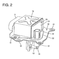
FIG. 2 is a perspective view of the terminal block with a mounted shielding shell when viewed obliquely from behind, -
FIG. 3 is a front view of the terminal block, -
FIG. 4 is a plan view of the terminal block, -
FIG. 5 is a section along A-A ofFIG. 4 , -
FIG. 6 is a section along B-B ofFIG. 5 , -
FIG. 7 is a section along C-C ofFIG. 3 , -
FIG. 8 is a plan view of a packing, -
FIG. 9 is a bottom view of the packing, -
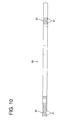
FIG. 10 is a section along D-D ofFIG. 8 , -
FIG. 11 is a plan view of a metal plate, -
FIG. 12 is a plan view of a terminal block according to a second embodiment, -
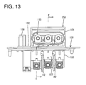
FIG. 13 is a front view of the terminal block, -
FIG. 14 is a section along E-E ofFIG. 13 , and -
FIG. 15 is a plan view of the metal plate. - A first particular embodiment of the present invention is described with reference to
FIGS. 1 to 11 . In this embodiment, a terminal block to be attached to a metal motor case (not shown) housing a motor (as an example of a "device") inside is illustrated as an example of a device connector. As shown inFIG. 3 , this terminal block includes ametal plate 30 to be attached and fixed to the motor case, aconnector housing 50 molded to be integral to themetal plate 30, and one or more (e.g. three) conductive plates (as an example of a "terminal fitting") 10 held or housed in theconnector housing 50 particularly while penetrating through themetal plate 30 in a plate thickness direction TD. Note that, in the following description, a vertical direction VD is a vertical direction inFIG. 3 , a lateral direction LD is a lateral direction inFIG. 3 , and forward and backward directions FBD are lateral directions inFIG. 7 with a shown left side referred to as a front side. - One or more one ends (first ends) of the
conductive plates 10 are to be connected (particularly bolt-fastened) to one or more, particularly a plurality of device-side busbars (not shown) provided in or at the motor case for electrical connection. On the other hand, in a power supply device for supplying power such as an inverter, one or more, particularly a plurality of wires are arranged to extend toward the motor case and a wire-side connector (not shown) is provided at end portions of these one or more wires. One or more wire-side terminals (not shown) connected to respective wire ends are provided in this wire-side connector, and these one or more wire-side terminals are connected (particularly bolt-fastened) to the one or more other ends of the respectiveconductive plates 10 for electrical connection. - Each
conductive plate 10 is formed by, after a conductive (particularly metal) plate with good electrical conductivity is punched or cut into a specified (predetermined or predeterminable) shape particularly by a press, performing a specified (predetermined or predeterminable) bending process on the punched or cut conductive (metal) plate as shown inFIG. 7 . Theconductive plate 10 includes a terminalmain portion 11 constituting a main part of theconductive plate 10, a wire-side fastening portion 12 extending laterally or forward from the lateral or upper end of the terminalmain portion 11, and a device-side fastening portion 13 provided at a lower end portion of the terminalmain portion 11. The terminalmain portion 11 particularly is formed to be longer than the wire-side fastening portion 12. - As shown in
FIG. 3 , the plurality of (e.g. three)conductive plates 10 particularly are arranged substantially side by side in the lateral direction LD. Further, the terminalmain portions 11 particularly are slightly cranked in the lateral direction LD at intermediate positions as shown by broken line inFIG. 3 . The wire-side fastening portions 12 and the device-side fastening portions 13 are each formed with abolt insertion hole 14 through which a fastening bolt (not shown) at least partly is insertable. - The terminal
main portion 11 of the conductive plate 10 (particularly arranged in the center or intermediate position out of the three conductive plates 10) substantially extends in the vertical direction VD and/or is substantially flat as shown inFIG. 7 . The lateral terminalmain portions 11, 11 (particularly of the both conductive plates located at the opposite left and right sides out of the three conductive plates 10) include each a facing portion bent forward to face the wire-side fastening portion 12 at an intermediate part (particularly a substantially vertically central part) of the terminalmain portion 11 although not shown, and the front end of this facing portion is bent downward particularly substantially at the same position as the front end of the wire-side fastening portion 12. - As shown in
FIG. 11 , themetal plate 30 particularly is made of a metal flat plate material as a base material and includes anopening 31 formed to penetrate in a plate thickness direction TD of the plate material. As shown inFIG. 2 , theconnector housing 50 particularly includes asmall connector portion 59 molded to be integral to themetal plate 30 and arranged to penetrate through theopening 31 in the vertical direction VD, a wire-sidefitting portion 51 arranged above (one side) themetal plate 30, a (particularly substantially plate-like) flange 52 arranged at or corresponding to the height position of themetal plate 30 and bulging out sideways (in a plane direction of the metal plate 30), and a device-sidefitting portion 53 arranged below (other side) themetal plate 30. Note that theflange 52 particularly corresponds to a "fixing portion". - As shown in
FIG. 1 , the wire-sidefitting portion 51 particularly substantially is in the form of a box long in the lateral direction and includes a front end opening 51 A (as a particular first opening) which is open in one direction (e.g. forward) and an upper end opening 51 B (as a particular second opening) which is open in another direction (e.g. upward). The wire-side connector is at least partly fittable or insertable into the wire-sidefitting portion 51 through the front end opening 51 A of the wire-sidefitting portion 51. - As shown in
FIG. 3 , one or more (e.g. three)nut accommodating portions 55 are formed (particularly substantially side by side in the lateral direction LD) in the wire-sidefitting portion 51. These one or more (e.g. three)nut accommodating portions 55 are respectively open to two sides such as forward and upward. Further, all the (three) nut accommodating portion(s) 55 is/are arranged to substantially face (particularly forward) through the front or first end opening 51 A and substantially face (particularly upward) through the upper or second end opening 51 B. One or more nuts N press-fitted through the front end opening 51 A from front particularly are so accommodated in thenut accommodating portions 55 that the axis lines of the nuts N are aligned with the vertical direction VD. - The wire-
side fastening portions 12 of theconductive plates 10 are arranged to close the upper end openings of thenut accommodating portions 55 as shown inFIGS. 3 and4 . Further, as shown inFIG. 7 , eachconductive plate 10 is arranged to penetrate through theopening 31 in the vertical direction VD and so held in theconnector housing 50 that the wire-side fastening portion 12 is substantially arranged around thebolt insertion hole 14 and at least partly exposed forward and/or upward in the wire-sidefitting portion 51 and, on the other hand, the device-side fastening portion 13 is substantially arranged around thebolt insertion hole 14 and at least partly exposed backward at the lower end portion of the device-sidefitting portion 53. Each wire-side fastening portion 12 is at least partly exposed to the outside through the upper end opening 51 B of the wire-sidefitting portion 51. That is, the upper end opening 51 B of the wire-sidefitting portion 51 particularly is or may be used as a service hole used to at least partly insert a tool or the like for a bolt fastening operation. The wire-side terminal is substantially placed on the wire-side fastening portion 12 and the tool is inserted inside through the upper end opening 51 B to threadably engage the fastening bolt with the nut N, whereby theconductive plate 10 and the wire-side terminal are electrically connected. Note that a service cover (not shown) is mounted on or to the upper end opening 51 B of the wire-sidefitting portion 51 after bolt fastening, thereby closing the upper end opening 51 B. - An escaping
recess 56 for allowing a leading end part of the fastening bolt penetrating through the nut N to escape when the fastening bolt is fastened to the nut N is provided below eachnut accommodating portion 55. The escapingrecess 56 particularly is formed to be narrower than thenut accommodating portion 55 in the lateral direction LD and integrally or unitarily formed with thenut accommodating portion 55 by a slide die. - As shown in
FIG. 2 , ametal shielding shell 70 at least partly covering the wire-sidefitting portion 51 except the rear surface is mounted on the wire-sidefitting portion 51. This shieldingshell 70 is formed by, after a conductive (particularly metal) plate with good electrical conductivity is punched or cut into a specified (predetermined or predeterminable) shape by a press, performing a specified (predetermined or predeterminable) bending process on the punched or cut conductive (metal) plate. The shieldingshell 70 includes a (particularly braided) fixingportion 71 having a laterally long cylindrical shape, and a fixingpiece 72 for fixing the shieldingshell 70 to themetal plate 30 and electrically connecting the shieldingshell 70 and the motor case by being fastened to the motor case together with themetal plate 30. Specifically, thebraided fixing portion 71 particularly is such that a braided wire provided to collectively cover shielded conductive paths of the wire-side connector is connected to a connection portion, particularly crimped against a crimp ring as the connection portion. - The
flange 52 is formed to at least partly cover an opening edge portion of theopening 31 over at least part of the circumference, particularly the substantially entire circumference, while exposing an outer peripheral edge portion of themetal plate 30. Thisflange 52 is composed of or comprises a wire-side flange 52A which at least partly covers a side of the wire-sidefitting portion 51 of the opening edge portion of theopening 31, a device-side flange 52B which at least partly covers a side of the device-sidefitting portion 52 thereof, and acoupling portion 52C (particularly arranged substantially along the inner circumferential surface of theopening 31 and) coupling the bothflanges side flange 52A and the device-side flange 52B sandwich themetal plate 30 in the plate thickness direction TD, and thecoupling portion 52C particularly is held in contact with the inner peripheral surface of theopening 31, whereby theconnector housing 50 is fixed or made integral to themetal plate 30. Specifically, as is clear fromFIG. 4 , the wire-side flange 52A of theflange 52 particularly is shaped to extend in the lateral direction LD and/or backward direction. As is clear fromFIGS. 5 and7 , the device-side flange 52B is formed to (particularly substantially entirely) cover a surface of themetal plate 30 at the side of the device-sidefitting portion 53. Note that the wire-side flange 52A particularly corresponds to a "one-side sliding portion", and the device-side flange 52B particularly corresponds to an "other-side sliding portion". - The
opening 31 particularly has a substantially trapezoidal shape. Further, the facing portions of theconductive plates 10 at the lateral (left and/or right) side(s) and/or the terminalmain portion 11 of the (particularly central)conductive plate 10 are arranged in theopening 31. On the other hand, athick portion 57 having a thick resin layer is formed particularly from a lower end portion of the wire-sidefitting portion 51 to an upper end portion of the device-sidefitting portion 53 as shown inFIG. 7 . That is, the one or more (e.g. three)conductive plates 10 having a complicated shape are arranged to penetrate through theopening 31 of themetal plate 30 in thisthick portion 57. - Further, one or more, particularly a plurality of mounting
holes 32 are formed in the outer peripheral edge portion of themetal plate 30. One or more fixing bolts or rivets (not shown) are to be at least partly inserted through these mountingholes 32 and fastened to the motor case, whereby the terminal block can be attached and fixed to the motor case. - The device-side
fitting portion 53 is housed into the motor case when the terminal block is fixed to the motor case. Further, as shown inFIG. 1 , one or more (e.g. three)nut accommodating portions 58 are formed in the device-sidefitting portion 53. Specifically, out of thesenut accommodating portions 58, thenut accommodating portion 58 located in the center or at an intermediate position is arranged behind the other nutaccommodating portions 58. In thenut accommodating portions 58 of the device-sidefitting portion 53, the fastening bolts are threadably engaged with respective nuts N to electrically connect theconductive plates 10 and the device-side busbars similar to thenut accommodating portions 55 of the wire-sidefitting portion 51. In this way, the wire-side terminals and the device-side busbars are electrically connected using theconductive plates 10 as intermediate terminals. - As shown in
FIG. 7 , the device-side flange 52B of theflange 52 is formed to bulge out sideways or laterally (along a direction parallel to a plane of the metal plate 30) more than the wire-side flange 52A. Apacking mounting groove 54 into which a (particularly substantially ring-shaped) packing 80 is to be mounted substantially is circumferentially formed in a part (corresponding to a particular "seal-mounting portion") of the device-side flange 52B bulging out from the wire-side flange 52A. The packing 80 is made of a resilient material such as rubber and includes one or more (e.g. two)annular lips 81 on a sealing surface to thepacking mounting groove 54 as shown inFIGS. 8 to 10 . A surface of the packing 80 opposite to the one with the (particularly both) annular lip(s) 81 serves as asurface sealing portion 82 to be surface sealed to the motor case. The motor case and the device-side flange 52B are fixed in a sealed manner via the packing 80 by fixing (particularly bolt-fastening) themetal plate 30 to the motor case. Since a sealing structure for the device-side flange 52B is formed by the (both) annular lip(s) 81 in this way, a pressing force required to press theannular lips 81 for a sealing purpose can be small. Accordingly, it is not necessary to ensure strength particularly by increasing the thickness of themetal plate 30 and sufficient sealing performance can be obtained with a smaller pressing force than in the case of using a metal plate made of aluminum die cast. - The
flange 52 in this embodiment is slidable relative to themetal plate 30. Specifically, the wire-side flange 52A is slidable relative to the upper surface of themetal plate 30, and the device-side flange 52B is slidable relative to the lower surface of themetal plate 30. Further, the wire-side flange 52A and the device-side flange 52B are coupled to each other by thecoupling portion 52C. Thiscoupling portion 52C is arranged to substantially face aninner surface 31 A of theopening 31. - Specifically, as shown in partial enlarged views of
FIGS. 5 and6 , a clearance C particularly is set between thecoupling portion 52C and theinner surface 31 A of theopening 31. This clearance C particularly is formed since synthetic resin shrinks more than metal in a cooling process after molding when themetal plate 30 and theconnector housing 50 are integrally formed. That is, the clearance C is not formed when molten resin is injected, but is formed when synthetic resin in theopening 31 shrinks while the wire-side flange 52A, the device-side flange 52B and thecoupling portion 52C slip toward theopening 31. - Although plating particularly is applied to the surfaces of the
metal plate 30 in this embodiment, the metal plate material as a base material may be used as it is without applying plating. Further, no process such as embossing is performed on themetal plate 30 except at theopening 31. Thus, the synthetic resin can slide on the surfaces of themetal plate 30 by expansion by heating or shrinkage by cooling. - Next, functions of this embodiment constructed as described above are described. First, one or more conductive plates 10 (e.g. three types of conductive plates 10) are set in a primary molding die (not shown), the die is clamped and primary molding resin is injected to form one or more (e.g. three) types of
cores 20. Subsequently, these one or more (e.g. three) types ofcores 20 are set in a secondary molding die (not shown), the die is clamped and secondary molding resin is injected to form the terminal block. Here, the secondary molding resin particularly shrinks toward theopening 31 in a cooling process after secondary molding, whereby the clearance C is formed between theinner surface 31 A of theopening 31 and thecoupling portion 52C. Since the secondary molding resin shrinks while slipping on the surfaces of themetal plate 30 in this cooling process, there is no likelihood that stress is accumulated in the secondary molding resin to form a crack. - Next, a thermal shock test conducted is described. The thermal shock test is a cold shock test which gives a thermal shock to the terminal block by repeating a low-temperature state (state lower than a normal temperature) and a high-temperature state (state higher than a normal temperature). When a transition is made from the low-temperature state to the high-temperature state, synthetic resin expands, whereby the wire-
side flange 52A slides on the upper surface of themetal plate 30 and the device-side flange 52B slides on the lower surface of themetal plate 30. Although this causes thecoupling portion 52C to approach theinner surface 31 A of theopening 31 to decrease or fill up the clearance C, a situation is not reached where thecoupling portion 52C receives stress from theinner surface 31 A of theopening 31 to form a crack. - Contrary to this, when a transition is made from the high-temperature state to the low-temperature state, the synthetic resin shrinks, whereby the wire-
side flange 52A slides on the upper surface of themetal plate 30 and the device-side flange 52B slides on the lower surface of themetal plate 30. Further, thecoupling portion 52C moves toward theopening 31 to form or increase the clearance C to theinner surface 31 A of theopening 31. Note that thecoupling portion 52C couples the wire-side flange 52A and the device-side flange 52B so that the bothflanges side flange 52A and that of the device-side flange 52B differ and themetal plate 30 is warped. - As described above, since the
flange 52 is slidable relative to themetal plate 30 in this embodiment, crack formation in the synthetic resin can be prevented. Further, since the wire-side flange 52A and the device-side flange 52B particularly are coupled by thecoupling portion 52C, the bothflanges metal plate 30 and the like can be prevented. Further, since the clearance C particularly is provided between theinner surface 31 A of theopening 31 and thecoupling portion 52C in a normal-temperature state, crack formation due to stress received by thecoupling portion 52C from theinner surface 31 A of theopening 31 in the high-temperature state of the thermal shock test can be prevented. Further, the one or moreannular lips 81 of the packing 80 are pressed by the device-side flange 52B and themetal plate 30 in thepacking mounting groove 54, wherefore theannular lips 81 can be pressed with a small pressing force and sufficient sealing performance can be obtained. - Accordingly, to suppress or reduce production cost by using a metal plate while preventing crack formation in synthetic resin, a terminal block is provided to be attached to case of a device such as a motor case. The terminal block includes a
metal plate 30 made of a metal plate material as a base material, formed with anopening 31 penetrating in a plate thickness direction TD of the plate material and to be attached and fixed to the motor case; aconnector housing 50 made of synthetic resin and fixed to themetal plate 30; andconductive plates 10 held in theconnector housing 50 while penetrating through theopening 30. Theconnector housing 50 includes aflange 52 which covers an opening edge portion of theopening 31 while exposing an outer peripheral edge portion of themetal plate 30. Theflange 52 includes a wire-side flange 52A slidable or movable relative to the upper surface of themetal plate 30, a device-side flange 52B slidable or movable relative to the lower surface of themetal plate 30 and acoupling portion 52C arranged in theopening 31 and at least partly coupling the bothflanges - Next, a second particular embodiment of the present invention is described with reference to
FIGS. 12 to 15 . Constructions of this embodiment corresponding to the first embodiment are identified by reference numerals which are the reference numerals of the first embodiment plus 100 and constructions, functions and effects similar to those of the first embodiment are not repeatedly described. The following description is centered on constructions different from the first embodiment. - As shown in
FIGS. 12 and15 , asmall opening 133 through which only asmall connector portion 159 at least partly is vertically inserted is formed in ametal plate 130 of this embodiment in addition to anopening 131 as openings through which aconnector housing 150 is vertically inserted. That is, a wire-sidefitting portion 151 and a device-sidefitting portion 153 are arranged in theopening 131 and thesmall connector portion 159 is arranged in thesmall opening 133. Themetal plate 130 particularly has a somewhat laterally long rectangular shape and mountingholes 132 are formed at four corners thereof. - As is clear from
FIG. 14 , theconnector housing 150 is not formed in two processes, i.e. primary molding and secondary molding unlike in the first embodiment, and is formed in one process by settingconductive plates 110 in a lower die of a molding die, clamping the molding die and injecting molten resin. The vertically extendingconductive plates 110 are insert-molded in theconnector housing 150, and wire-side fastening portions 112 vertically extend in flush with terminalmain portions 111. - As shown in
FIG. 14 , athick portion 157 particularly is formed with one or more mold removal holes H1 which communicate with escapingrecesses 156 and vertically extend. A pair of mold removal holes H1 are provided in correspondence with upper and lower escapingrecesses 156. These mold removal holes H1 prevent the formation of voids in thethick portion 157. Further, as shown inFIG. 13 , thethick portion 157 is formed with one or more, particularly a plurality of mold removal holes H2 with an open front side. The formation of voids in thethick portion 157 is also prevented by these mold removal holes H2. - The
small connector portion 159 and the wire-sidefitting portion 151, and thesmall connector portion 159 and the device-sidefitting portion 153 are respectively coupled to each other via acommon flange 152. As in the first embodiment, theflange 152 is slidable relative to themetal plate 130. Accordingly, crack formation caused by a temperature variation in a cooling process after the molding of theconnector housing 150 and a thermal shock test can be prevented. - The present invention is not limited to the above described and illustrated embodiments. For example, the following embodiments are also included in the technical scope of the present invention.
- (1) Although the flange is integrally formed with the metal plate in the above embodiments, the flange may be formed separately from the metal plate and may be mounted later according to the present invention. That is, the one-side sliding portion and the other-side sliding portion may be arranged to sandwich the metal plate from the opposite sides and integrally assembled by a bolt.
- (2) Although a clearance is provided between the coupling portion and the inner surface of the opening in the above embodiments, no clearance may be provided according to the present invention, for example, such as when the opening is small and no crack is formed even if the synthetic resin in the opening expands and stress is received from the inner surface of the opening.
- (3) Although the packing formed with the annular lips on one surface is used in the above embodiments, a packing formed with surface sealing portions on both surfaces may be used according to the present invention.
- (4) Although the
flange 52 at least partly covers the opening edge portion of theopening 31 over the entire circumference in the above embodiment, at least one flange (fixing portion) may be so formed as to cover a part of the opening edge portion of theopening 31 according to the present invention. This leads to a cost reduction by reducing the amount of the resin and/or reduces the influence of thermal shrinkage by reducing the amount of the resin covering the opening edge portion of the opening, thereby reducing friction produced between the metal plate and the fixing portion and making the fixing portion more easily slidable relative to the metal plate. - (5) Although the device-
side flange 52B is formed to be longer (or project more outward) than the wire-side flange 52A in the above embodiment, the device-side flange and the wire-side flange may be formed to have the substantially same length or the device-side flange may be formed to be shorter than the wire-side flange according to the present invention. - (6) Although the
packing mounting groove 54 is integrally or unitarily formed in the device-side flange 52B in the above embodiment, a seal-mounting portion may be formed separately from the device-side flange and the packing mounting groove may be formed in this seal-mounting portion. That is, the seal-mounting portion may be formed in conformity with the mounting position of the packing. - (7) Although in the above embodiments the
plate 30 is a metal plate being made of metal plate material, it should be understood that theplate 30 may be made of any other material such as a composite material, a layered material or the like. -
10, 110 conductive plate (terminal fitting) 30, 130 metal plate (plate) 31, 131 opening 31A. 131A inner surface 50, 150 connector housing 51, 151 wire-side fitting portion (first connecting portion) 52, 152 flange (fixing portion) 52A, 152A wire-side flange (one-side sliding portion) 52B, 152B device-side flange (other-side sliding portion) 52C, 152C coupling portion 53, 153 device-side fitting portion (second connecting portion) 54 seal-mounting portion 57, 157 thick portion 80, 180 packing 81, 181 annular lip 131 small opening C clearance
Claims (15)
- A device connector to be attached to a case of a device, comprising:a plate (30; 130) made of a plate material as a base material, formed with an opening (31; 131) penetrating in a plate thickness direction (TD) of the plate material and to be attached and fixed to the case of the device;a connector housing (50; 150) made of synthetic resin and fixed to the plate (30; 130); andat least one terminal fitting (10; 110) held in the connector housing (50; 150) while penetrating through the opening (31; 131);wherein:the connector housing (50; 150) includes a fixing portion (52; 152) which at least partly covers an opening edge portion of the opening (31; 131) while exposing an outer peripheral edge portion of the plate (30; 130); andthe fixing portion (52; 152) includes a one-side sliding portion (52A; 152A) slidable relative to one surface side of the plate (30; 130), an other-side sliding portion (52B; 152B) slidable relative to the other surface side of the plate (30; 130) and a coupling portion (52C; 152C) substantially arranged in the opening (31; 131) and coupling the one-side sliding portion (52A; 152A) and the other-side sliding portion (52B; 152B).
- A device connector according to claim 1, wherein the plate (30; 130) is a metal plate (30; 130) made of a metal plate material as a base material.
- A device connector according to any one of the preceding claims, wherein a clearance (C) is formed between the coupling portion (52C; 152C) and the inner surface of the opening (31; 131) facing the coupling portion (52C; 152C) particularly in a state where the molded connector housing (50; 150) is cooled to a normal temperature.
- A device connector according to any one of the preceding claims, wherein a seal-mounting portion (54) made of synthetic resin at least partly is circumferentially provided on a part of a surface of the plate (30; 130), which will face the case of the device, radially outward of the fixing portion (52; 152); and
the case of the device and the seal-mounting portion (54) are fixed in a sealed state via a packing (80; 180). - A device connector according to claim 4, wherein a plurality of annular lips (81; 181) are provided on a sealing surface of the packing (80; 180) to the seal-mounting portion (54).
- A device connector according to any one of the preceding claims, wherein plating is applied to the surfaces of the metal plate (30; 130).
- A device connector according to any one of the preceding claims, wherein one of the one-side sliding portion (52A; 152A) and the other-side sliding portion (52B; 152B) is formed to project more outward than the other of the one-side sliding portion (52A; 152A) and the other-side sliding portion (52B; 152B).
- A device connector according to any one of the preceding claims, wherein the terminal fitting (10; 110) is in the form of a conductive plate (10; 110) including a terminal main portion (11), a wire-side fastening portion (12) provided at one end of the terminal main portion (11), particularly extending at an angle different from 0° or 180°, preferably substantially perpendicular to the terminal main portion (11), and a device-side fastening portion (13) provided at another end of the terminal main portion (11).
- A device connector according to any one of the preceding claims, wherein the connector housing (50; 150) comprises a first connecting portion (51; 151) to be connected to a connector and a second connecting portion (53; 153) being arranged in the opening (31; 131) and to be connected with the device.
- A device connector according to claim 9, wherein a thick portion (57; 157) having a thick resin layer is formed from a portion of the first connecting portion (51; 151) to a portion of the second connecting portion (53; 153).
- A device connector according to claim 10, wherein the terminal fitting (10; 110) is arranged to penetrate through the opening (31; 131) of the plate (30; 130) in the thick portion (57; 157).
- A method of producing a device connector to be attached to a case of a device, comprising:setting at least one terminal fitting (10; 110) in a primary molding die,clamping the die andinjecting primary molding resin to form at least one type of core (20);thensetting a plate (30; 130) made of a plate material as a base material, formed with an opening (31; 131) penetrating in a plate thickness direction (TD) of the plate material and the formed core (20) at least partly arranged inside the opening (31; 131) in a secondary molding die,clamping the die andinjecting secondary molding resin to form a connector housing (50; 150) made of synthetic resin and fixed to the plate (30; 130), wherein the connector housing (50; 150) is formed to include a fixing portion (52; 152) which at least partly covers an opening edge portion of the opening (31; 131) while exposing an outer peripheral edge portion of the plate (30; 130); and wherein the fixing portion (52; 152) is formed to include a one-side sliding portion (52A; 152A) slidable relative to one surface side of the plate (30; 130), an other-side sliding portion (52B; 152B) slidable relative to the other surface side of the plate (30; 130) and a coupling portion (52C; 152C) substantially arranged in the opening (31; 131) and coupling the one-side sliding portion (52A; 152A) and the other-side sliding portion (52B; 152B).
- A method according to claim 12, wherein the secondary molding resin shrinks toward the opening (31; 131) in a cooling process after secondary molding, whereby the clearance (C) is formed between an inner surface (31A; 131 A) of the opening (31; 131) and the coupling portion (52C; 152C).
- A method according to claim 12 or 13, wherein a seal-mounting portion (54) made of synthetic resin at least partly is circumferentially provided on a part of a surface of the plate (30; 130), which will face the case of the device, radially outward of the fixing portion (52; 152).
- A method according to any one of the preceding claims 12 to 14, wherein the plate (30; 130) is a metal plate (30; 130) and plating is applied to the surfaces of the metal plate (30; 130).
Applications Claiming Priority (1)
| Application Number | Priority Date | Filing Date | Title |
|---|---|---|---|
| JP2011056334A JP5641345B2 (en) | 2011-03-15 | 2011-03-15 | Connector for equipment |
Publications (2)
| Publication Number | Publication Date |
|---|---|
| EP2500996A1 true EP2500996A1 (en) | 2012-09-19 |
| EP2500996B1 EP2500996B1 (en) | 2017-08-30 |
Family
ID=45929376
Family Applications (1)
| Application Number | Title | Priority Date | Filing Date |
|---|---|---|---|
| EP12001109.3A Not-in-force EP2500996B1 (en) | 2011-03-15 | 2012-02-20 | Device connector and method of producing it |
Country Status (4)
| Country | Link |
|---|---|
| US (1) | US8771010B2 (en) |
| EP (1) | EP2500996B1 (en) |
| JP (1) | JP5641345B2 (en) |
| CN (1) | CN102738670B (en) |
Cited By (1)
| Publication number | Priority date | Publication date | Assignee | Title |
|---|---|---|---|---|
| CN109075519A (en) * | 2016-04-19 | 2018-12-21 | 三菱电机株式会社 | Method for manufacturing connector device |
Families Citing this family (20)
| Publication number | Priority date | Publication date | Assignee | Title |
|---|---|---|---|---|
| JP5626047B2 (en) * | 2011-03-15 | 2014-11-19 | 住友電装株式会社 | Connector for equipment |
| JP5569442B2 (en) * | 2011-03-15 | 2014-08-13 | 住友電装株式会社 | Connector for equipment |
| JP5751875B2 (en) * | 2011-03-22 | 2015-07-22 | 矢崎総業株式会社 | Shield connector |
| US9308877B2 (en) * | 2011-03-31 | 2016-04-12 | Toyota Jidosha Kabushiki Kaisha | Power control unit |
| JP6155057B2 (en) * | 2013-03-08 | 2017-06-28 | Kyb株式会社 | Busbar unit manufacturing method and busbar unit |
| JP2015095354A (en) * | 2013-11-12 | 2015-05-18 | 住友電装株式会社 | Connector for apparatus and method for manufacturing the same |
| JP6194272B2 (en) * | 2014-04-01 | 2017-09-06 | 本田技研工業株式会社 | Motor structure |
| JP6536431B2 (en) * | 2016-02-29 | 2019-07-03 | 住友電装株式会社 | Resin molding |
| WO2019230518A1 (en) * | 2018-05-28 | 2019-12-05 | 住友電装株式会社 | Connector assembly |
| DE102018218163A1 (en) * | 2018-10-24 | 2020-04-30 | Zf Friedrichshafen Ag | Interface module, inverter and vehicle |
| US11171440B2 (en) * | 2019-03-20 | 2021-11-09 | Aptiv Technologies Limited | Backing plate for mounting and sealing an electrical connector to an intermediate surface |
| DE102020126962B4 (en) * | 2020-01-21 | 2026-01-29 | Hanon Systems | Arrangement for connecting electrical terminals and device for driving a compressor with the arrangement |
| DE102020201418A1 (en) | 2020-02-05 | 2021-08-05 | Volkswagen Aktiengesellschaft | Electrical contacting module, motor vehicle and method for producing an electrical contacting module |
| JP7396156B2 (en) * | 2020-03-26 | 2023-12-12 | 住友電装株式会社 | Terminal block |
| JP6955047B2 (en) * | 2020-03-31 | 2021-10-27 | 本田技研工業株式会社 | Power control unit |
| CN112103691A (en) * | 2020-10-09 | 2020-12-18 | 江苏万聚电气有限公司 | Power supply wiring device |
| JP2022111645A (en) * | 2021-01-20 | 2022-08-01 | 住友電装株式会社 | Terminal block and terminal block unit |
| FR3124661A1 (en) * | 2021-06-29 | 2022-12-30 | Valeo Equipements Electriques Moteur | Together to form a waterproof interconnector |
| JP7512992B2 (en) * | 2021-10-27 | 2024-07-09 | 住友電装株式会社 | connector |
| CN118659154B (en) * | 2024-08-19 | 2025-02-07 | 河南正铂建筑工程有限公司 | A safe electrical connector to prevent open circuit |
Citations (3)
| Publication number | Priority date | Publication date | Assignee | Title |
|---|---|---|---|---|
| US6076258A (en) * | 1996-04-23 | 2000-06-20 | Yazaki Corporation | Method for insert molding and method for producing a connector |
| US20020016100A1 (en) * | 2000-07-25 | 2002-02-07 | Yazaki Coroporation | Connector supporting structure |
| JP2009032500A (en) | 2007-07-26 | 2009-02-12 | Sumitomo Wiring Syst Ltd | Connector for equipment |
Family Cites Families (15)
| Publication number | Priority date | Publication date | Assignee | Title |
|---|---|---|---|---|
| JPS5773256A (en) * | 1980-10-22 | 1982-05-07 | Aisin Warner Ltd | Sealing wire terminal |
| JPH0416394Y2 (en) * | 1985-01-18 | 1992-04-13 | ||
| US4647129A (en) * | 1985-12-20 | 1987-03-03 | Amp Incorporated | Electrical connector |
| JP3075445B2 (en) * | 1992-11-04 | 2000-08-14 | 矢崎総業株式会社 | Mounting method and mounting structure of connector to panel |
| JPH0742018U (en) * | 1993-12-28 | 1995-07-21 | 矢崎総業株式会社 | Equipment directly attached waterproof connector |
| US5511990A (en) * | 1994-11-14 | 1996-04-30 | General Motors Corporation | Electrical interface connector assembly |
| CH689853A5 (en) * | 1995-06-28 | 1999-12-15 | Schurter Ag | Elektrotechnisches component. |
| US5775944A (en) * | 1996-08-19 | 1998-07-07 | General Motors Corporation | Sealed connector-to-body interface |
| CN1194478A (en) * | 1997-03-26 | 1998-09-30 | 惠特克公司 | Connector |
| JP3687717B2 (en) * | 1998-02-18 | 2005-08-24 | 矢崎総業株式会社 | Movable connector connection structure |
| JP3425541B2 (en) * | 1999-08-23 | 2003-07-14 | 株式会社オートネットワーク技術研究所 | Shield connector |
| JP2002124329A (en) * | 2000-10-13 | 2002-04-26 | Auto Network Gijutsu Kenkyusho:Kk | Board mounted connector |
| DE10352768B4 (en) * | 2002-11-19 | 2008-07-10 | Sumitomo Wiring Systems, Ltd., Yokkaichi | Connector and connector assembly |
| JP4015590B2 (en) * | 2003-06-04 | 2007-11-28 | 住友電装株式会社 | Case seal structure and assembly method thereof |
| JP5233959B2 (en) * | 2009-11-05 | 2013-07-10 | 住友電装株式会社 | Connector for equipment |
-
2011
- 2011-03-15 JP JP2011056334A patent/JP5641345B2/en not_active Expired - Fee Related
-
2012
- 2012-02-20 EP EP12001109.3A patent/EP2500996B1/en not_active Not-in-force
- 2012-03-06 US US13/412,883 patent/US8771010B2/en active Active
- 2012-03-14 CN CN201210066854.0A patent/CN102738670B/en not_active Expired - Fee Related
Patent Citations (3)
| Publication number | Priority date | Publication date | Assignee | Title |
|---|---|---|---|---|
| US6076258A (en) * | 1996-04-23 | 2000-06-20 | Yazaki Corporation | Method for insert molding and method for producing a connector |
| US20020016100A1 (en) * | 2000-07-25 | 2002-02-07 | Yazaki Coroporation | Connector supporting structure |
| JP2009032500A (en) | 2007-07-26 | 2009-02-12 | Sumitomo Wiring Syst Ltd | Connector for equipment |
Cited By (3)
| Publication number | Priority date | Publication date | Assignee | Title |
|---|---|---|---|---|
| CN109075519A (en) * | 2016-04-19 | 2018-12-21 | 三菱电机株式会社 | Method for manufacturing connector device |
| EP3447860A4 (en) * | 2016-04-19 | 2019-07-03 | Mitsubishi Electric Corporation | METHOD FOR MANUFACTURING CONNECTOR DEVICE |
| US11152755B2 (en) | 2016-04-19 | 2021-10-19 | Mitsubishi Electric Corporation | Connector device manufacturing method |
Also Published As
| Publication number | Publication date |
|---|---|
| JP2012195065A (en) | 2012-10-11 |
| US20120238134A1 (en) | 2012-09-20 |
| EP2500996B1 (en) | 2017-08-30 |
| CN102738670B (en) | 2015-04-22 |
| JP5641345B2 (en) | 2014-12-17 |
| CN102738670A (en) | 2012-10-17 |
| US8771010B2 (en) | 2014-07-08 |
Similar Documents
| Publication | Publication Date | Title |
|---|---|---|
| EP2500996B1 (en) | Device connector and method of producing it | |
| EP2500995B1 (en) | Production method for a connector | |
| EP2500997B1 (en) | Connector and method of producing it | |
| EP2500991B1 (en) | Mounting structure for shielding shell and mounting method therefor | |
| EP2500985B1 (en) | Device connector and production method therefor | |
| JP5741344B2 (en) | connector | |
| US11217930B2 (en) | Seal cover | |
| EP2573875B1 (en) | Connector and method of assembling it | |
| US10666002B2 (en) | Wiring harness connecting structure for housed circuit assembly | |
| KR101022874B1 (en) | Connector with multiple concave-convex structure and joining method | |
| JP2013089436A (en) | Conducting path | |
| US20200412049A1 (en) | Connector | |
| CN207818971U (en) | Connector |
Legal Events
| Date | Code | Title | Description |
|---|---|---|---|
| PUAI | Public reference made under article 153(3) epc to a published international application that has entered the european phase |
Free format text: ORIGINAL CODE: 0009012 |
|
| AK | Designated contracting states |
Kind code of ref document: A1 Designated state(s): AL AT BE BG CH CY CZ DE DK EE ES FI FR GB GR HR HU IE IS IT LI LT LU LV MC MK MT NL NO PL PT RO RS SE SI SK SM TR |
|
| AX | Request for extension of the european patent |
Extension state: BA ME |
|
| 17P | Request for examination filed |
Effective date: 20130307 |
|
| 17Q | First examination report despatched |
Effective date: 20150608 |
|
| GRAP | Despatch of communication of intention to grant a patent |
Free format text: ORIGINAL CODE: EPIDOSNIGR1 |
|
| RIC1 | Information provided on ipc code assigned before grant |
Ipc: B29C 45/14 20060101ALI20170316BHEP Ipc: H01R 43/24 20060101AFI20170316BHEP Ipc: B29C 45/16 20060101ALI20170316BHEP Ipc: H01R 43/18 20060101ALI20170316BHEP Ipc: H01R 13/405 20060101ALI20170316BHEP Ipc: H01R 13/74 20060101ALN20170316BHEP |
|
| RIC1 | Information provided on ipc code assigned before grant |
Ipc: H01R 43/18 20060101ALI20170323BHEP Ipc: B29C 45/14 20060101ALI20170323BHEP Ipc: H01R 13/405 20060101ALI20170323BHEP Ipc: B29C 45/16 20060101ALI20170323BHEP Ipc: H01R 43/24 20060101AFI20170323BHEP Ipc: H01R 13/74 20060101ALN20170323BHEP |
|
| INTG | Intention to grant announced |
Effective date: 20170413 |
|
| GRAS | Grant fee paid |
Free format text: ORIGINAL CODE: EPIDOSNIGR3 |
|
| GRAA | (expected) grant |
Free format text: ORIGINAL CODE: 0009210 |
|
| AK | Designated contracting states |
Kind code of ref document: B1 Designated state(s): AL AT BE BG CH CY CZ DE DK EE ES FI FR GB GR HR HU IE IS IT LI LT LU LV MC MK MT NL NO PL PT RO RS SE SI SK SM TR |
|
| REG | Reference to a national code |
Ref country code: GB Ref legal event code: FG4D |
|
| REG | Reference to a national code |
Ref country code: CH Ref legal event code: EP |
|
| REG | Reference to a national code |
Ref country code: AT Ref legal event code: REF Ref document number: 924475 Country of ref document: AT Kind code of ref document: T Effective date: 20170915 |
|
| REG | Reference to a national code |
Ref country code: IE Ref legal event code: FG4D |
|
| REG | Reference to a national code |
Ref country code: DE Ref legal event code: R096 Ref document number: 602012036506 Country of ref document: DE |
|
| REG | Reference to a national code |
Ref country code: NL Ref legal event code: MP Effective date: 20170830 |
|
| REG | Reference to a national code |
Ref country code: LT Ref legal event code: MG4D |
|
| REG | Reference to a national code |
Ref country code: AT Ref legal event code: MK05 Ref document number: 924475 Country of ref document: AT Kind code of ref document: T Effective date: 20170830 |
|
| PG25 | Lapsed in a contracting state [announced via postgrant information from national office to epo] |
Ref country code: NO Free format text: LAPSE BECAUSE OF FAILURE TO SUBMIT A TRANSLATION OF THE DESCRIPTION OR TO PAY THE FEE WITHIN THE PRESCRIBED TIME-LIMIT Effective date: 20171130 Ref country code: LT Free format text: LAPSE BECAUSE OF FAILURE TO SUBMIT A TRANSLATION OF THE DESCRIPTION OR TO PAY THE FEE WITHIN THE PRESCRIBED TIME-LIMIT Effective date: 20170830 Ref country code: FI Free format text: LAPSE BECAUSE OF FAILURE TO SUBMIT A TRANSLATION OF THE DESCRIPTION OR TO PAY THE FEE WITHIN THE PRESCRIBED TIME-LIMIT Effective date: 20170830 Ref country code: AT Free format text: LAPSE BECAUSE OF FAILURE TO SUBMIT A TRANSLATION OF THE DESCRIPTION OR TO PAY THE FEE WITHIN THE PRESCRIBED TIME-LIMIT Effective date: 20170830 Ref country code: HR Free format text: LAPSE BECAUSE OF FAILURE TO SUBMIT A TRANSLATION OF THE DESCRIPTION OR TO PAY THE FEE WITHIN THE PRESCRIBED TIME-LIMIT Effective date: 20170830 Ref country code: SE Free format text: LAPSE BECAUSE OF FAILURE TO SUBMIT A TRANSLATION OF THE DESCRIPTION OR TO PAY THE FEE WITHIN THE PRESCRIBED TIME-LIMIT Effective date: 20170830 |
|
| PG25 | Lapsed in a contracting state [announced via postgrant information from national office to epo] |
Ref country code: GR Free format text: LAPSE BECAUSE OF FAILURE TO SUBMIT A TRANSLATION OF THE DESCRIPTION OR TO PAY THE FEE WITHIN THE PRESCRIBED TIME-LIMIT Effective date: 20171201 Ref country code: ES Free format text: LAPSE BECAUSE OF FAILURE TO SUBMIT A TRANSLATION OF THE DESCRIPTION OR TO PAY THE FEE WITHIN THE PRESCRIBED TIME-LIMIT Effective date: 20170830 Ref country code: LV Free format text: LAPSE BECAUSE OF FAILURE TO SUBMIT A TRANSLATION OF THE DESCRIPTION OR TO PAY THE FEE WITHIN THE PRESCRIBED TIME-LIMIT Effective date: 20170830 Ref country code: BG Free format text: LAPSE BECAUSE OF FAILURE TO SUBMIT A TRANSLATION OF THE DESCRIPTION OR TO PAY THE FEE WITHIN THE PRESCRIBED TIME-LIMIT Effective date: 20171130 Ref country code: RS Free format text: LAPSE BECAUSE OF FAILURE TO SUBMIT A TRANSLATION OF THE DESCRIPTION OR TO PAY THE FEE WITHIN THE PRESCRIBED TIME-LIMIT Effective date: 20170830 Ref country code: IS Free format text: LAPSE BECAUSE OF FAILURE TO SUBMIT A TRANSLATION OF THE DESCRIPTION OR TO PAY THE FEE WITHIN THE PRESCRIBED TIME-LIMIT Effective date: 20171230 |
|
| PG25 | Lapsed in a contracting state [announced via postgrant information from national office to epo] |
Ref country code: NL Free format text: LAPSE BECAUSE OF FAILURE TO SUBMIT A TRANSLATION OF THE DESCRIPTION OR TO PAY THE FEE WITHIN THE PRESCRIBED TIME-LIMIT Effective date: 20170830 |
|
| PG25 | Lapsed in a contracting state [announced via postgrant information from national office to epo] |
Ref country code: CZ Free format text: LAPSE BECAUSE OF FAILURE TO SUBMIT A TRANSLATION OF THE DESCRIPTION OR TO PAY THE FEE WITHIN THE PRESCRIBED TIME-LIMIT Effective date: 20170830 Ref country code: PL Free format text: LAPSE BECAUSE OF FAILURE TO SUBMIT A TRANSLATION OF THE DESCRIPTION OR TO PAY THE FEE WITHIN THE PRESCRIBED TIME-LIMIT Effective date: 20170830 Ref country code: RO Free format text: LAPSE BECAUSE OF FAILURE TO SUBMIT A TRANSLATION OF THE DESCRIPTION OR TO PAY THE FEE WITHIN THE PRESCRIBED TIME-LIMIT Effective date: 20170830 Ref country code: DK Free format text: LAPSE BECAUSE OF FAILURE TO SUBMIT A TRANSLATION OF THE DESCRIPTION OR TO PAY THE FEE WITHIN THE PRESCRIBED TIME-LIMIT Effective date: 20170830 |
|
| PG25 | Lapsed in a contracting state [announced via postgrant information from national office to epo] |
Ref country code: SM Free format text: LAPSE BECAUSE OF FAILURE TO SUBMIT A TRANSLATION OF THE DESCRIPTION OR TO PAY THE FEE WITHIN THE PRESCRIBED TIME-LIMIT Effective date: 20170830 Ref country code: EE Free format text: LAPSE BECAUSE OF FAILURE TO SUBMIT A TRANSLATION OF THE DESCRIPTION OR TO PAY THE FEE WITHIN THE PRESCRIBED TIME-LIMIT Effective date: 20170830 Ref country code: IT Free format text: LAPSE BECAUSE OF FAILURE TO SUBMIT A TRANSLATION OF THE DESCRIPTION OR TO PAY THE FEE WITHIN THE PRESCRIBED TIME-LIMIT Effective date: 20170830 Ref country code: SK Free format text: LAPSE BECAUSE OF FAILURE TO SUBMIT A TRANSLATION OF THE DESCRIPTION OR TO PAY THE FEE WITHIN THE PRESCRIBED TIME-LIMIT Effective date: 20170830 |
|
| REG | Reference to a national code |
Ref country code: DE Ref legal event code: R097 Ref document number: 602012036506 Country of ref document: DE |
|
| PLBE | No opposition filed within time limit |
Free format text: ORIGINAL CODE: 0009261 |
|
| STAA | Information on the status of an ep patent application or granted ep patent |
Free format text: STATUS: NO OPPOSITION FILED WITHIN TIME LIMIT |
|
| 26N | No opposition filed |
Effective date: 20180531 |
|
| PG25 | Lapsed in a contracting state [announced via postgrant information from national office to epo] |
Ref country code: SI Free format text: LAPSE BECAUSE OF FAILURE TO SUBMIT A TRANSLATION OF THE DESCRIPTION OR TO PAY THE FEE WITHIN THE PRESCRIBED TIME-LIMIT Effective date: 20170830 |
|
| REG | Reference to a national code |
Ref country code: CH Ref legal event code: PL |
|
| PG25 | Lapsed in a contracting state [announced via postgrant information from national office to epo] |
Ref country code: MC Free format text: LAPSE BECAUSE OF FAILURE TO SUBMIT A TRANSLATION OF THE DESCRIPTION OR TO PAY THE FEE WITHIN THE PRESCRIBED TIME-LIMIT Effective date: 20170830 |
|
| GBPC | Gb: european patent ceased through non-payment of renewal fee |
Effective date: 20180220 |
|
| REG | Reference to a national code |
Ref country code: IE Ref legal event code: MM4A |
|
| REG | Reference to a national code |
Ref country code: BE Ref legal event code: MM Effective date: 20180228 |
|
| PG25 | Lapsed in a contracting state [announced via postgrant information from national office to epo] |
Ref country code: LI Free format text: LAPSE BECAUSE OF NON-PAYMENT OF DUE FEES Effective date: 20180228 Ref country code: LU Free format text: LAPSE BECAUSE OF NON-PAYMENT OF DUE FEES Effective date: 20180220 Ref country code: CH Free format text: LAPSE BECAUSE OF NON-PAYMENT OF DUE FEES Effective date: 20180228 |
|
| REG | Reference to a national code |
Ref country code: FR Ref legal event code: ST Effective date: 20181031 |
|
| PG25 | Lapsed in a contracting state [announced via postgrant information from national office to epo] |
Ref country code: IE Free format text: LAPSE BECAUSE OF NON-PAYMENT OF DUE FEES Effective date: 20180220 |
|
| PG25 | Lapsed in a contracting state [announced via postgrant information from national office to epo] |
Ref country code: FR Free format text: LAPSE BECAUSE OF NON-PAYMENT OF DUE FEES Effective date: 20180228 Ref country code: BE Free format text: LAPSE BECAUSE OF NON-PAYMENT OF DUE FEES Effective date: 20180228 Ref country code: GB Free format text: LAPSE BECAUSE OF NON-PAYMENT OF DUE FEES Effective date: 20180220 |
|
| REG | Reference to a national code |
Ref country code: DE Ref legal event code: R084 Ref document number: 602012036506 Country of ref document: DE |
|
| PG25 | Lapsed in a contracting state [announced via postgrant information from national office to epo] |
Ref country code: MT Free format text: LAPSE BECAUSE OF NON-PAYMENT OF DUE FEES Effective date: 20180220 |
|
| PG25 | Lapsed in a contracting state [announced via postgrant information from national office to epo] |
Ref country code: TR Free format text: LAPSE BECAUSE OF FAILURE TO SUBMIT A TRANSLATION OF THE DESCRIPTION OR TO PAY THE FEE WITHIN THE PRESCRIBED TIME-LIMIT Effective date: 20170830 |
|
| PG25 | Lapsed in a contracting state [announced via postgrant information from national office to epo] |
Ref country code: HU Free format text: LAPSE BECAUSE OF FAILURE TO SUBMIT A TRANSLATION OF THE DESCRIPTION OR TO PAY THE FEE WITHIN THE PRESCRIBED TIME-LIMIT; INVALID AB INITIO Effective date: 20120220 Ref country code: PT Free format text: LAPSE BECAUSE OF FAILURE TO SUBMIT A TRANSLATION OF THE DESCRIPTION OR TO PAY THE FEE WITHIN THE PRESCRIBED TIME-LIMIT Effective date: 20170830 |
|
| PG25 | Lapsed in a contracting state [announced via postgrant information from national office to epo] |
Ref country code: MK Free format text: LAPSE BECAUSE OF NON-PAYMENT OF DUE FEES Effective date: 20170830 Ref country code: CY Free format text: LAPSE BECAUSE OF FAILURE TO SUBMIT A TRANSLATION OF THE DESCRIPTION OR TO PAY THE FEE WITHIN THE PRESCRIBED TIME-LIMIT Effective date: 20170830 |
|
| PG25 | Lapsed in a contracting state [announced via postgrant information from national office to epo] |
Ref country code: AL Free format text: LAPSE BECAUSE OF FAILURE TO SUBMIT A TRANSLATION OF THE DESCRIPTION OR TO PAY THE FEE WITHIN THE PRESCRIBED TIME-LIMIT Effective date: 20170830 |
|
| P01 | Opt-out of the competence of the unified patent court (upc) registered |
Effective date: 20230517 |
|
| PGFP | Annual fee paid to national office [announced via postgrant information from national office to epo] |
Ref country code: DE Payment date: 20231228 Year of fee payment: 13 |
|
| REG | Reference to a national code |
Ref country code: DE Ref legal event code: R119 Ref document number: 602012036506 Country of ref document: DE |
|
| PG25 | Lapsed in a contracting state [announced via postgrant information from national office to epo] |
Ref country code: DE Free format text: LAPSE BECAUSE OF NON-PAYMENT OF DUE FEES Effective date: 20250902 |