EP2500920A1 - Composite electronic component - Google Patents
Composite electronic component Download PDFInfo
- Publication number
- EP2500920A1 EP2500920A1 EP12159178A EP12159178A EP2500920A1 EP 2500920 A1 EP2500920 A1 EP 2500920A1 EP 12159178 A EP12159178 A EP 12159178A EP 12159178 A EP12159178 A EP 12159178A EP 2500920 A1 EP2500920 A1 EP 2500920A1
- Authority
- EP
- European Patent Office
- Prior art keywords
- body portion
- magnetic body
- dielectric body
- dielectric
- layer
- Prior art date
- Legal status (The legal status is an assumption and is not a legal conclusion. Google has not performed a legal analysis and makes no representation as to the accuracy of the status listed.)
- Withdrawn
Links
- 239000002131 composite material Substances 0.000 title claims abstract description 93
- 239000007769 metal material Substances 0.000 claims abstract description 13
- 239000000463 material Substances 0.000 claims description 191
- 238000005245 sintering Methods 0.000 description 23
- 238000004519 manufacturing process Methods 0.000 description 22
- 230000008602 contraction Effects 0.000 description 18
- 239000000203 mixture Substances 0.000 description 15
- 238000009792 diffusion process Methods 0.000 description 13
- 239000011701 zinc Substances 0.000 description 13
- 238000001816 cooling Methods 0.000 description 11
- 239000000919 ceramic Substances 0.000 description 9
- 239000002612 dispersion medium Substances 0.000 description 9
- 238000000034 method Methods 0.000 description 9
- 229910000859 α-Fe Inorganic materials 0.000 description 9
- GWEVSGVZZGPLCZ-UHFFFAOYSA-N Titan oxide Chemical compound O=[Ti]=O GWEVSGVZZGPLCZ-UHFFFAOYSA-N 0.000 description 8
- 230000000694 effects Effects 0.000 description 8
- 239000011521 glass Substances 0.000 description 8
- 239000005388 borosilicate glass Substances 0.000 description 7
- 238000005266 casting Methods 0.000 description 7
- 239000000470 constituent Substances 0.000 description 7
- 239000011347 resin Substances 0.000 description 7
- 229920005989 resin Polymers 0.000 description 7
- ZFZQOKHLXAVJIF-UHFFFAOYSA-N zinc;boric acid;dihydroxy(dioxido)silane Chemical compound [Zn+2].OB(O)O.O[Si](O)([O-])[O-] ZFZQOKHLXAVJIF-UHFFFAOYSA-N 0.000 description 7
- LYCAIKOWRPUZTN-UHFFFAOYSA-N Ethylene glycol Chemical compound OCCO LYCAIKOWRPUZTN-UHFFFAOYSA-N 0.000 description 6
- VYPSYNLAJGMNEJ-UHFFFAOYSA-N Silicium dioxide Chemical compound O=[Si]=O VYPSYNLAJGMNEJ-UHFFFAOYSA-N 0.000 description 6
- 239000003990 capacitor Substances 0.000 description 6
- 239000011148 porous material Substances 0.000 description 6
- 239000000843 powder Substances 0.000 description 6
- 238000003825 pressing Methods 0.000 description 6
- 239000002002 slurry Substances 0.000 description 6
- 239000003795 chemical substances by application Substances 0.000 description 5
- 239000003999 initiator Substances 0.000 description 5
- 229910017518 Cu Zn Inorganic materials 0.000 description 4
- 229910017752 Cu-Zn Inorganic materials 0.000 description 4
- 229910017943 Cu—Zn Inorganic materials 0.000 description 4
- LFQSCWFLJHTTHZ-UHFFFAOYSA-N Ethanol Chemical compound CCO LFQSCWFLJHTTHZ-UHFFFAOYSA-N 0.000 description 4
- PNEYBMLMFCGWSK-UHFFFAOYSA-N aluminium oxide Inorganic materials [O-2].[O-2].[O-2].[Al+3].[Al+3] PNEYBMLMFCGWSK-UHFFFAOYSA-N 0.000 description 4
- 238000005336 cracking Methods 0.000 description 4
- 238000002474 experimental method Methods 0.000 description 4
- 239000012948 isocyanate Substances 0.000 description 4
- 150000002513 isocyanates Chemical class 0.000 description 4
- 230000002093 peripheral effect Effects 0.000 description 4
- 239000004848 polyfunctional curative Substances 0.000 description 4
- 229920000642 polymer Polymers 0.000 description 4
- URAYPUMNDPQOKB-UHFFFAOYSA-N triacetin Chemical group CC(=O)OCC(OC(C)=O)COC(C)=O URAYPUMNDPQOKB-UHFFFAOYSA-N 0.000 description 4
- CSCPPACGZOOCGX-UHFFFAOYSA-N Acetone Chemical compound CC(C)=O CSCPPACGZOOCGX-UHFFFAOYSA-N 0.000 description 3
- UHOVQNZJYSORNB-UHFFFAOYSA-N Benzene Chemical compound C1=CC=CC=C1 UHOVQNZJYSORNB-UHFFFAOYSA-N 0.000 description 3
- KFZMGEQAYNKOFK-UHFFFAOYSA-N Isopropanol Chemical compound CC(C)O KFZMGEQAYNKOFK-UHFFFAOYSA-N 0.000 description 3
- OKKJLVBELUTLKV-UHFFFAOYSA-N Methanol Chemical compound OC OKKJLVBELUTLKV-UHFFFAOYSA-N 0.000 description 3
- YXFVVABEGXRONW-UHFFFAOYSA-N Toluene Chemical compound CC1=CC=CC=C1 YXFVVABEGXRONW-UHFFFAOYSA-N 0.000 description 3
- 229910052681 coesite Inorganic materials 0.000 description 3
- 229910052802 copper Inorganic materials 0.000 description 3
- 229910052593 corundum Inorganic materials 0.000 description 3
- 229910052906 cristobalite Inorganic materials 0.000 description 3
- 150000002148 esters Chemical class 0.000 description 3
- 239000000696 magnetic material Substances 0.000 description 3
- 239000000178 monomer Substances 0.000 description 3
- 238000000465 moulding Methods 0.000 description 3
- VLKZOEOYAKHREP-UHFFFAOYSA-N n-Hexane Chemical compound CCCCCC VLKZOEOYAKHREP-UHFFFAOYSA-N 0.000 description 3
- -1 phosphate ester Chemical class 0.000 description 3
- 239000002243 precursor Substances 0.000 description 3
- 239000000377 silicon dioxide Substances 0.000 description 3
- 229910052709 silver Inorganic materials 0.000 description 3
- 229910052682 stishovite Inorganic materials 0.000 description 3
- 229910052905 tridymite Inorganic materials 0.000 description 3
- 229910001845 yogo sapphire Inorganic materials 0.000 description 3
- QCXNXRUTKSIZND-UHFFFAOYSA-N 6-(dimethylamino)hexan-1-ol Chemical compound CN(C)CCCCCCO QCXNXRUTKSIZND-UHFFFAOYSA-N 0.000 description 2
- 239000004925 Acrylic resin Substances 0.000 description 2
- 229920000178 Acrylic resin Polymers 0.000 description 2
- PEDCQBHIVMGVHV-UHFFFAOYSA-N Glycerine Chemical compound OCC(O)CO PEDCQBHIVMGVHV-UHFFFAOYSA-N 0.000 description 2
- 239000005057 Hexamethylene diisocyanate Substances 0.000 description 2
- MHAJPDPJQMAIIY-UHFFFAOYSA-N Hydrogen peroxide Chemical compound OO MHAJPDPJQMAIIY-UHFFFAOYSA-N 0.000 description 2
- 239000005058 Isophorone diisocyanate Substances 0.000 description 2
- MCMNRKCIXSYSNV-UHFFFAOYSA-N Zirconium dioxide Chemical compound O=[Zr]=O MCMNRKCIXSYSNV-UHFFFAOYSA-N 0.000 description 2
- 150000001412 amines Chemical class 0.000 description 2
- ROOXNKNUYICQNP-UHFFFAOYSA-N ammonium persulfate Chemical compound [NH4+].[NH4+].[O-]S(=O)(=O)OOS([O-])(=O)=O ROOXNKNUYICQNP-UHFFFAOYSA-N 0.000 description 2
- 229910002113 barium titanate Inorganic materials 0.000 description 2
- WMWLMWRWZQELOS-UHFFFAOYSA-N bismuth(iii) oxide Chemical compound O=[Bi]O[Bi]=O WMWLMWRWZQELOS-UHFFFAOYSA-N 0.000 description 2
- 239000003822 epoxy resin Substances 0.000 description 2
- 239000001087 glyceryl triacetate Substances 0.000 description 2
- 235000013773 glyceryl triacetate Nutrition 0.000 description 2
- RRAMGCGOFNQTLD-UHFFFAOYSA-N hexamethylene diisocyanate Chemical compound O=C=NCCCCCCN=C=O RRAMGCGOFNQTLD-UHFFFAOYSA-N 0.000 description 2
- JEIPFZHSYJVQDO-UHFFFAOYSA-N iron(III) oxide Inorganic materials O=[Fe]O[Fe]=O JEIPFZHSYJVQDO-UHFFFAOYSA-N 0.000 description 2
- NIMLQBUJDJZYEJ-UHFFFAOYSA-N isophorone diisocyanate Chemical compound CC1(C)CC(N=C=O)CC(C)(CN=C=O)C1 NIMLQBUJDJZYEJ-UHFFFAOYSA-N 0.000 description 2
- NUJOXMJBOLGQSY-UHFFFAOYSA-N manganese dioxide Chemical compound O=[Mn]=O NUJOXMJBOLGQSY-UHFFFAOYSA-N 0.000 description 2
- 239000002184 metal Substances 0.000 description 2
- 229910052751 metal Inorganic materials 0.000 description 2
- 239000004033 plastic Substances 0.000 description 2
- 229920003023 plastic Polymers 0.000 description 2
- 239000003495 polar organic solvent Substances 0.000 description 2
- 229920000647 polyepoxide Polymers 0.000 description 2
- 229920001451 polypropylene glycol Polymers 0.000 description 2
- 230000009257 reactivity Effects 0.000 description 2
- 239000000126 substance Substances 0.000 description 2
- 229920002803 thermoplastic polyurethane Polymers 0.000 description 2
- DVKJHBMWWAPEIU-UHFFFAOYSA-N toluene 2,4-diisocyanate Chemical compound CC1=CC=C(N=C=O)C=C1N=C=O DVKJHBMWWAPEIU-UHFFFAOYSA-N 0.000 description 2
- 229960002622 triacetin Drugs 0.000 description 2
- IMNIMPAHZVJRPE-UHFFFAOYSA-N triethylenediamine Chemical compound C1CN2CCN1CC2 IMNIMPAHZVJRPE-UHFFFAOYSA-N 0.000 description 2
- UWFRVQVNYNPBEF-UHFFFAOYSA-N 1-(2,4-dimethylphenyl)propan-1-one Chemical compound CCC(=O)C1=CC=C(C)C=C1C UWFRVQVNYNPBEF-UHFFFAOYSA-N 0.000 description 1
- IVIDDMGBRCPGLJ-UHFFFAOYSA-N 2,3-bis(oxiran-2-ylmethoxy)propan-1-ol Chemical compound C1OC1COC(CO)COCC1CO1 IVIDDMGBRCPGLJ-UHFFFAOYSA-N 0.000 description 1
- HDPLHDGYGLENEI-UHFFFAOYSA-N 2-[1-(oxiran-2-ylmethoxy)propan-2-yloxymethyl]oxirane Chemical compound C1OC1COC(C)COCC1CO1 HDPLHDGYGLENEI-UHFFFAOYSA-N 0.000 description 1
- AOBIOSPNXBMOAT-UHFFFAOYSA-N 2-[2-(oxiran-2-ylmethoxy)ethoxymethyl]oxirane Chemical compound C1OC1COCCOCC1CO1 AOBIOSPNXBMOAT-UHFFFAOYSA-N 0.000 description 1
- CCJAYIGMMRQRAO-UHFFFAOYSA-N 2-[4-[(2-hydroxyphenyl)methylideneamino]butyliminomethyl]phenol Chemical compound OC1=CC=CC=C1C=NCCCCN=CC1=CC=CC=C1O CCJAYIGMMRQRAO-UHFFFAOYSA-N 0.000 description 1
- UPMLOUAZCHDJJD-UHFFFAOYSA-N 4,4'-Diphenylmethane Diisocyanate Chemical compound C1=CC(N=C=O)=CC=C1CC1=CC=C(N=C=O)C=C1 UPMLOUAZCHDJJD-UHFFFAOYSA-N 0.000 description 1
- HRPVXLWXLXDGHG-UHFFFAOYSA-N Acrylamide Chemical compound NC(=O)C=C HRPVXLWXLXDGHG-UHFFFAOYSA-N 0.000 description 1
- 229920002126 Acrylic acid copolymer Polymers 0.000 description 1
- PIICEJLVQHRZGT-UHFFFAOYSA-N Ethylenediamine Chemical compound NCCN PIICEJLVQHRZGT-UHFFFAOYSA-N 0.000 description 1
- CERQOIWHTDAKMF-UHFFFAOYSA-N Methacrylic acid Chemical compound CC(=C)C(O)=O CERQOIWHTDAKMF-UHFFFAOYSA-N 0.000 description 1
- KWYHDKDOAIKMQN-UHFFFAOYSA-N N,N,N',N'-tetramethylethylenediamine Chemical compound CN(C)CCN(C)C KWYHDKDOAIKMQN-UHFFFAOYSA-N 0.000 description 1
- 229910019142 PO4 Inorganic materials 0.000 description 1
- 239000002202 Polyethylene glycol Substances 0.000 description 1
- 239000004721 Polyphenylene oxide Substances 0.000 description 1
- 229910007565 Zn—Cu Inorganic materials 0.000 description 1
- 150000001298 alcohols Chemical class 0.000 description 1
- IMUDHTPIFIBORV-UHFFFAOYSA-N aminoethylpiperazine Chemical compound NCCN1CCNCC1 IMUDHTPIFIBORV-UHFFFAOYSA-N 0.000 description 1
- 229910001870 ammonium persulfate Inorganic materials 0.000 description 1
- WPKYZIPODULRBM-UHFFFAOYSA-N azane;prop-2-enoic acid Chemical compound N.OC(=O)C=C WPKYZIPODULRBM-UHFFFAOYSA-N 0.000 description 1
- ODINCKMPIJJUCX-UHFFFAOYSA-N calcium oxide Inorganic materials [Ca]=O ODINCKMPIJJUCX-UHFFFAOYSA-N 0.000 description 1
- 150000001875 compounds Chemical class 0.000 description 1
- 229920001577 copolymer Polymers 0.000 description 1
- 150000004985 diamines Chemical class 0.000 description 1
- 239000003989 dielectric material Substances 0.000 description 1
- 125000000118 dimethyl group Chemical group [H]C([H])([H])* 0.000 description 1
- XTDYIOOONNVFMA-UHFFFAOYSA-N dimethyl pentanedioate Chemical compound COC(=O)CCCC(=O)OC XTDYIOOONNVFMA-UHFFFAOYSA-N 0.000 description 1
- 150000002009 diols Chemical class 0.000 description 1
- 239000002270 dispersing agent Substances 0.000 description 1
- 239000006185 dispersion Substances 0.000 description 1
- 125000004185 ester group Chemical group 0.000 description 1
- 235000011187 glycerol Nutrition 0.000 description 1
- SYECJBOWSGTPLU-UHFFFAOYSA-N hexane-1,1-diamine Chemical compound CCCCCC(N)N SYECJBOWSGTPLU-UHFFFAOYSA-N 0.000 description 1
- UCNNJGDEJXIUCC-UHFFFAOYSA-L hydroxy(oxo)iron;iron Chemical compound [Fe].O[Fe]=O.O[Fe]=O UCNNJGDEJXIUCC-UHFFFAOYSA-L 0.000 description 1
- 230000000977 initiatory effect Effects 0.000 description 1
- 150000002540 isothiocyanates Chemical class 0.000 description 1
- 238000010030 laminating Methods 0.000 description 1
- ZIUHHBKFKCYYJD-UHFFFAOYSA-N n,n'-methylenebisacrylamide Chemical compound C=CC(=O)NCNC(=O)C=C ZIUHHBKFKCYYJD-UHFFFAOYSA-N 0.000 description 1
- 239000003960 organic solvent Substances 0.000 description 1
- 239000010452 phosphate Substances 0.000 description 1
- 229920001281 polyalkylene Polymers 0.000 description 1
- 229920000768 polyamine Polymers 0.000 description 1
- 229920005646 polycarboxylate Polymers 0.000 description 1
- 229920000728 polyester Chemical group 0.000 description 1
- 229920000570 polyether Polymers 0.000 description 1
- 229920001223 polyethylene glycol Polymers 0.000 description 1
- 239000005056 polyisocyanate Substances 0.000 description 1
- 229920001228 polyisocyanate Polymers 0.000 description 1
- 150000007519 polyprotic acids Polymers 0.000 description 1
- 150000004072 triols Chemical class 0.000 description 1
- XLYOFNOQVPJJNP-UHFFFAOYSA-N water Substances O XLYOFNOQVPJJNP-UHFFFAOYSA-N 0.000 description 1
Images




Classifications
-
- H—ELECTRICITY
- H01—ELECTRIC ELEMENTS
- H01G—CAPACITORS; CAPACITORS, RECTIFIERS, DETECTORS, SWITCHING DEVICES, LIGHT-SENSITIVE OR TEMPERATURE-SENSITIVE DEVICES OF THE ELECTROLYTIC TYPE
- H01G4/00—Fixed capacitors; Processes of their manufacture
- H01G4/30—Stacked capacitors
-
- H—ELECTRICITY
- H01—ELECTRIC ELEMENTS
- H01F—MAGNETS; INDUCTANCES; TRANSFORMERS; SELECTION OF MATERIALS FOR THEIR MAGNETIC PROPERTIES
- H01F17/00—Fixed inductances of the signal type
- H01F17/0006—Printed inductances
- H01F17/0013—Printed inductances with stacked layers
-
- H—ELECTRICITY
- H01—ELECTRIC ELEMENTS
- H01G—CAPACITORS; CAPACITORS, RECTIFIERS, DETECTORS, SWITCHING DEVICES, LIGHT-SENSITIVE OR TEMPERATURE-SENSITIVE DEVICES OF THE ELECTROLYTIC TYPE
- H01G4/00—Fixed capacitors; Processes of their manufacture
- H01G4/40—Structural combinations of fixed capacitors with other electric elements, the structure mainly consisting of a capacitor, e.g. RC combinations
-
- H—ELECTRICITY
- H01—ELECTRIC ELEMENTS
- H01F—MAGNETS; INDUCTANCES; TRANSFORMERS; SELECTION OF MATERIALS FOR THEIR MAGNETIC PROPERTIES
- H01F17/00—Fixed inductances of the signal type
- H01F17/0006—Printed inductances
- H01F17/0013—Printed inductances with stacked layers
- H01F2017/0026—Multilayer LC-filter
Definitions
- the present invention relates to a composite electronic component.
- Patent Document 1 describes a LC composite component serving as a composite electronic component.
- the LC composite component is formed by jointing a part made of a dielectric material (hereinafter, this part is called the “dielectric body portion”) and a part made of a magnetic material (hereinafter, this part is called the “magnetic body portion”) via a part made of a specific material (hereinafter, this part is called the “intermediate part”).
- the LC composite component plural pairs of electrodes including conductive bodies are provided inside of the dielectric body portion, the dielectric body portion functions as a capacitor, a coil including a conductive body is formed inside of the magnetic body portion, and the magnetic body portion functions as an inductor.
- the dielectric body portion of the composite electronic component described in Patent Document 1 is formed of a material of crystallized glass containing SiO 2 , Al 2 O 3 , CaO, and the like, the material containing Ni-Cu-Zn ferrite. Meanwhile, the magnetic body portion of the composite electronic component described in Patent Document 1 is formed of magnetic ferrite powder. Therefore, a thermal expansion coefficient of the dielectric body portion and a thermal expansion coefficient of the magnetic body portion are different from each other.
- a composite electronic component is also described in Patent Document 2.
- the composite electronic component is also formed by jointing a dielectric body portion and a magnetic body portion via an intermediate part.
- plural pairs of electrodes including conductive bodies are provided inside of the dielectric body portion, the dielectric body portion functions as a capacitor, a coil including a conductive body is formed inside of the magnetic body portion, and the magnetic body portion functions as an inductor.
- the dielectric body portion of the composite electronic component described in Patent Document 2 is formed of ceramic such as TiO 2 and Ba 3 O 4 .
- the magnetic body portion of the composite electronic component described in Patent Document 2 is formed of magnetic oxide ferrite.
- a thermal expansion coefficient of the dielectric body portion and a thermal expansion coefficient of the magnetic body portion are different from each other in the composite electronic component described in Patent Document 2.
- a material in which one of glass, alumina, and ferrite is mixed with a material of the dielectric body portion is used as a material of the intermediate part, which realizes a thermal expansion coefficient of the intermediate part so as to absorb a difference between contraction of the dielectric body portion and contraction of the magnetic body portion at the cooling stage of the sintered dielectric and magnetic body portions.
- a composite electronic component is also described in Patent Document 3 ( JP4020886B ).
- the composite electronic component is also formed by jointing a dielectric body portion and a magnetic body portion via an intermediate part.
- plural pairs of electrodes including conductive bodies are provided inside of the dielectric body portion, the dielectric body portion functions as a capacitor, a coil including a conductive body is formed inside of the magnetic body portion, and the magnetic body portion functions as an inductor.
- the dielectric body portion of the composite electronic component described in Patent Document 3 is formed of Ti ceramic, for example.
- the magnetic body portion of the composite electronic component described in Patent Document 3 is formed of Ni-Cu-Zn magnetic ferrite, for example.
- Patent Document 3 Fe-Zn-Cu nonmagnetic ferrite and zinc borosilicate glass are used as materials of the intermediate part, which realizes a thermal expansion coefficient of the intermediate part so as to absorb a difference between contraction of the dielectric body portion and contraction of the magnetic body portion at the cooling stage of the sintered dielectric and magnetic body portions.
- Patent Documents 1 to 3 for jointing the dielectric and magnetic body portions having different thermal expansion coefficients from each other, the dielectric body portion and the magnetic body portion are jointed via the intermediate part having the thermal expansion coefficient so as to absorb the difference between the contraction of the dielectric body portion and the contraction of the magnetic body portion at the cooling stage of the sintered dielectric and magnetic body portions, so that the dielectric body portion and the magnetic body portion are favorably jointed.
- the composite electronic component formed by jointing the dielectric body portion and the magnetic body portion via the intermediate part as described above, when the composite electronic component was sintered, there is sometimes a case where part of the material of the dielectric body portion diffuses inside of the magnetic body portion, part of the material of the magnetic body portion diffuses inside of the dielectric body portion, or part of the material of the intermediate part diffuses inside of the dielectric body portion or inside of the magnetic body portion. Such diffusion may result in an insufficient joint strength between the dielectric body portion and the magnetic body portion via the intermediate part.
- a property of the magnetic body portion may be deteriorated.
- a property of the dielectric body portion may be deteriorated.
- the dielectric body portion and the magnetic body portion contain materials or elements other than Zn, and such materials or elements cannot be suppressed from diffusing by the intermediate part. Diffusion of such materials or elements between the dielectric body portion and the magnetic body portion may also result in an insufficient joint strength between the dielectric body portion and the magnetic body portion, or deteriorated properties of the dielectric body portion and the magnetic body portion.
- An object of the present invention is, in a composite electronic component having a dielectric body portion inside of which a conductive body is provided, and a magnetic body portion inside of which a conductive body is provided, to suppress a material or an element of a part surrounding the conductive body of the dielectric body portion from diffusing inside of the magnetic body portion, or to suppress a material or an element of a part surrounding the conductive body of the magnetic body portion from diffusing inside of the dielectric body portion.
- the invention of the present application relates to a composite electronic component having a dielectric body portion inside of which a conductive body is provided, and a magnetic body portion inside of which a conductive body is provided.
- a layer made of a metal material is arranged between the dielectric body portion and the magnetic body portion as an intermediate layer.
- the material and the element are collectively called the "dielectric body material”
- the dielectric body material is suppressed from diffusing inside of the magnetic body portion.
- the material and the element are collectively called the “magnetic body material”
- the magnetic body material is suppressed from diffusing inside of the dielectric body portion. This further ensures a sufficiently high joint strength between the dielectric body portion and the magnetic body portion, and sufficiently enhanced properties of the dielectric body portion and the magnetic body portion.
- the intermediate layer is made of the same material or the same element as a material or an element of the conductive body of the dielectric body portion, or the same material or the same element as a material or an element of the conductive body of the magnetic body portion.
- the intermediate layer is formed of the same material or the same element as the material or the element of the conductive body of the dielectric body portion, or the same material or the same element as the material or the element of the conductive body of the magnetic body portion; which facilitates manufacturing of the composite electronic component of the present invention.
- the conductive body of the dielectric body portion and the conductive body of the magnetic body portion are formed of the same material or the same element.
- the material or the element of the intermediate layer is the same as the material or the element of the conductive body of the dielectric body portion, and the material or the element of the conductive body of the magnetic body portion; which facilitates manufacturing of the composite electronic component of the present invention.
- a layer formed of a material having a higher joint strength to the dielectric body portion and the intermediate layer than a predetermined strength is arranged between the dielectric body portion and the intermediate layer as a joint layer, or a layer formed of a material having a higher joint strength to the magnetic body portion and the intermediate layer than a predetermined strength is arranged between the magnetic body portion and the intermediate layer as a joint layer.
- the joint strength between the joint layer and the dielectric body portion and the intermediate layer is relatively high, even if joint strength between the intermediate layer and the dielectric body portion is low and thus joint strength between the dielectric body portion and the magnetic body portion via the intermediate layer is low; which ensures a relatively high joint strength between the dielectric body portion and the magnetic body portion via the joint layer.
- joint strength between the joint layer and the magnetic body portion and the intermediate layer is relatively high, even if joint strength between the intermediate layer and the magnetic body portion is low and thus the joint strength between the dielectric body portion and the magnetic body portion via the intermediate layer is low; which ensures a relatively high joint strength between the dielectric body portion and the magnetic body portion via the joint layer.
- the reference numeral 10 denotes a composite electronic component of the first embodiment.
- the composite electronic component 10 has a rectangular parallelepiped shape.
- the composite electronic component 10 has a dielectric body portion 11, a magnetic body portion 12, an intermediate layer 13, a first joint layer 14, a second joint layer 15, and external electrodes 16A to 16H as constituent elements thereof.
- the dielectric body portion 11 and the magnetic body portion 12 have a rectangular parallelepiped shape.
- the intermediate layer 13 and the first joint layer 14 also have a rectangular parallelepiped shape, and thickness of these layers is relatively small, it can also be considered that the layers have a plate shape.
- the second joint layer 15 has a plate shape surrounding a circumference of the intermediate layer 13.
- an upper part seen on a paper plane of Fig. 2 is referred to as the "upper side”.
- a lower part is the “slower side”
- a left part is the “left side”
- a right part is the “right side”, in the following description.
- the dielectric body portion 11 has a plurality of conductive bodies 11C, and a main body 11B.
- the main body 11B surrounds the conductive bodies 11C.
- the conductive bodies 11C are arranged inside of the main body 11B, that is, inside of the dielectric body portion 11.
- the conductive bodies 11C have a plate shape.
- the conductive bodies 11C are arranged in parallel to each other, and plural pairs of the conductive bodies are connected to predetermined external terminals, respectively. Therefore, the dielectric body portion 11 functions as a capacitor. That is, a plurality of capacitors is formed inside of the dielectric body portion 11, and the capacitors are connected to the predetermined external terminals, respectively.
- the main body 11B of the dielectric body portion 11 is formed of a dielectric body material such as a BaTiO 3 -based dielectric body material and a TiO 2 -based dielectric body material.
- the conductive bodies 11C of the dielectric body portion 11 are formed of a metal material such as Ag and Cu, that is, a conductive body material.
- the magnetic body portion 12 has a plurality of conductive bodies 12C, and a main body 12B.
- the main body 12B surrounds the conductive bodies 12C.
- the conductive bodies 12C are arranged inside of the main body 12B, that is, inside of the magnetic body portion 12.
- the conductive bodies 12C have a coil shape.
- ends of the coils are exposed onto wall surfaces of the magnetic body portion 12.
- one ends of the conductive bodies 12C forming the coils are connected to the electrode 16A or 16C, and the other ends are connected to the electrode 16D or 16F. Therefore, the magnetic body portion 12 functions as an inductor. That is, a plurality of inductors is formed inside of the magnetic body portion 12, and the inductors are respectively connected to predetermined external terminals.
- the main body 12B of the magnetic body portion 12 is formed of a magnetic material such as a Ni-Cu-Zn-based ferrite material and a Mn-Zn-based ferrite material.
- the conductive bodies 12C of the magnetic body portion 12 are formed of a metal material such as Ag and Cu, that is, a conductive body material.
- the intermediate layer 13 is arranged between the dielectric body portion 11 and the first joint layer 14 and surrounded by the second joint layer 15.
- a part of the second joint layer 15 on the left side of the intermediate layer 13 is referred to as the "left part of the second joint layer” and denoted by the reference numeral 15L
- a part of the second joint layer 15 on the right side of the intermediate layer 13 is referred to as the "right part of the second joint layer” and denoted by the reference numeral 15R.
- the intermediate layer 13 is arranged between the dielectric body portion 11, the first joint layer 14, the left part 15L of the second joint layer, and the right part 15R of the second joint layer.
- An entire upper wall surface of the intermediate layer 13 is in contact with part of a lower wall surface of the main body 11B of the dielectric body portion 11, an entire lower wall surface thereof is in contact with part of an upper wall surface of the first joint layer 14, and entire end surfaces thereof are in contact with entire inner end surfaces of the second joint layer 15. That is, the upper wall surface of the intermediate layer 13 is in contact with only an area of the lower wall surface of the main body 11B of the dielectric body portion 11 excluding an area close to wall surfaces of the dielectric body portion 11.
- the lower wall surface of the intermediate layer 13 is in contact with only an area of the upper wall surface of the first joint layer 14 excluding an area close to the wall surfaces of the dielectric body portion 11. Since the entire outer end surfaces of the intermediate layer 13 are in contact with the inner end surfaces of the second joint layer 15, the intermediate layer 13 is not exposed onto wall surfaces of the composite electronic component 10 in no contact with the external terminal electrodes 16A to 16H.
- the intermediate layer 13 is formed of a metal material such as Ag and Cu.
- the first joint layer 14 is arranged between the intermediate layer 13, the second joint layer 15, and the magnetic body portion 12. Part of the upper wall surface of the first joint layer 14 is in contact with the entire lower wall surface of the intermediate layer 13 and an entire lower wall surface of the second joint layer 15, and an entire lower wall surface thereof is in contact with an entire upper wall surface of the main body 12B of the magnetic body portion 12. That is, a peripheral area of the upper wall surface of the first joint layer 14 is in contact with the entire lower wall surface of the second joint layer 15, and an area excluding the peripheral area is in contact with the entire lower wall surface of the intermediate layer 13. End surfaces of the first joint layer 14 are exposed onto the wall surfaces of the composite electronic component 10 in contact with the external terminal electrodes 16A to 16H.
- the first joint layer 14 is formed of a material in which a dielectric body material such as a Ba-Ti-Zn-based dielectric body material, glass such as zinc borosilicate glass, and CuO are mixed.
- the second joint layer 15 is arranged between the dielectric body portion 11 and the first joint layer 14 and surrounds the intermediate layer 13.
- An entire upper wall surface of the second joint layer 15 is in contact with part of the lower wall surface of the main body 11B of the dielectric body portion 11, the entire inner end surfaces thereof are in contact with the entire outer end surfaces of the intermediate layer 13, and the entire lower wall surface thereof is in contact with part of the upper wall surface of the first joint layer 14.
- Outer end surfaces of the second joint layer 15 are exposed onto the wall surfaces of the composite electronic component 10 in contact with the external terminal electrodes 16A to 16H.
- the second joint layer 15 is formed of a material in which a dielectric body material such as a Ba-Ti-Zn-based dielectric body material, glass such as zinc borosilicate glass, and CuO are mixed. That is, the second joint layer 15 is formed of the material having the same composition as the material of the first joint layer 14. However, a ratio of the dielectric body material, a ratio of glass, and a ratio of CuO in the material of the second joint layer 15 may be respectively the same as corresponding ratios in the material of the first joint layer 14, or the ratio of glass and the ratio of CuO in the material of the second joint layer 15 may be respectively larger than the corresponding ratios in the material of the first joint layer 14.
- a ratio of the dielectric body material, a ratio of glass, and a ratio of CuO in the material of the second joint layer 15 may be respectively the same as corresponding ratios in the material of the first joint layer 14, or the ratio of glass and the ratio of CuO in the material of the second joint layer 15 may be respectively larger than the corresponding ratio
- the composite electronic component 10 of the first embodiment is manufactured by assembling the dielectric body portion 11, the magnetic body portion 12, the intermediate layer 13, the first joint layer 14, and the second joint layer 15 in the positional relationship described above so as to produce a laminated body, sintering the laminated body so as to produce a sintered body, and forming the external electrodes 16A to 16H in the sintered body.
- part of a material or an element of the main body 11B of the dielectric body portion 11 (hereinafter, the material and the element are collectively called the "dielectric body material”) is apt to diffuse inside of the magnetic body portion 12.
- the dielectric body material diffuses inside of the magnetic body portion 12 through the first joint layer 14.
- the diffused material lowers joint strength between the first joint layer 14 and the magnetic body portion 12 in the finally manufactured composite electronic component 10, and also lowers an electric property of the magnetic body portion 12 in the finally manufactured composite electronic component 10.
- a composition of the dielectric body portion 11 is also changed by element diffusion, and thus a sintering property and an electric property of the dielectric body portion 11 are also deteriorated.
- the intermediate layer 13 is provided, and the intermediate layer 13 is formed of a metal material. That is, the intermediate layer 13 has a structure of metal bond, and thus the dielectric body material cannot diffuse in the intermediate layer 13. As a result, diffusion of the dielectric body material inside of the magnetic body portion 12 via the first joint layer 14 is suppressed. Therefore, a sufficiently high joint strength is ensured between the first joint layer 14 and the magnetic body portion 12 in the finally manufactured composite electronic component 10 (and eventually, joint strength between the dielectric body portion 11 and the magnetic body portion 12), and sufficiently enhanced electric properties of the dielectric body portion 11 and the magnetic body portion 12 are ensured.
- the laminated body including the dielectric body portion 11, the magnetic body portion 12, the first joint layer 14, the second joint layer 15, and the intermediate layer 13 was sintered according to the first embodiment, few pores were found in the magnetic body portion 12 and the first joint layer 14, the joint strength between the first joint layer 14 and the magnetic body portion 12 was high, and the electric properties of the dielectric body portion 11 and the magnetic body portion 12 were enhanced.
- part of the material or an element of the main body 12B of the magnetic body portion 12 (hereinafter, the material and the element are collectively called the “magnetic body material”) is apt to diffuse inside of the dielectric body portion 11. Without the intermediate layer 13, the magnetic body material diffuses inside of the dielectric body portion 11 through the first joint layer 14.
- the diffused magnetic body material lowers joint strength between the first joint layer 14 and the dielectric body portion 11 in the finally manufactured composite electronic component 10 (without the intermediate layer 13, the second joint layer 15 is not provided as well, and thus the upper wall surface of the first joint layer 14 is in direct contact with a lower wall surface of the dielectric body portion 11), and also lowers the electric property of the dielectric body portion 11 in the finally manufactured composite electronic component 10. Further, a composition of the magnetic body portion 12 is also changed by element diffusion, so that a sintering property and the electric property of the magnetic body portion 12 are also deteriorated.
- the intermediate layer 13 is provided, and the intermediate layer 13 is formed of a metal material. That is, the intermediate layer 13 has a structure of metal bond, and thus the magnetic body material cannot diffuse in the intermediate layer 13. As a result, diffusion of the magnetic body material inside of the dielectric body portion 11 via the first joint layer 14 is suppressed. Therefore, a sufficiently high joint strength is ensured between the first joint layer 14 and the dielectric body portion 11 via the intermediate layer 13 in the finally manufactured composite electronic component 10 (and eventually, the joint strength between the magnetic body portion 12 and the dielectric body portion 11), and sufficiently enhanced electric properties of the dielectric body portion 11 and the magnetic body portion 12 are ensured.
- the laminated body including the dielectric body portion 11, the magnetic body portion 12, the first joint layer 14, the second joint layer 15, and the intermediate layer 13 was sintered according to the first embodiment, few pores were found in the dielectric body portion 11 and the first joint layer 14, joint strength between the first joint layer 14 and the intermediate layer 13 and joint strength between the intermediate layer 13 and the dielectric body portion 11 were high, and the electric properties of the dielectric body portion 11 and the magnetic body portion 12 were enhanced.
- the material of the conductive bodies 11C of the dielectric body portion 11 that is, the conductive body material of the dielectric body portion
- the material of the conductive bodies 12C of the magnetic body portion 12 that is, the conductive body material of the magnetic body portion
- the material of the intermediate layer 13 is the same as both the conductive body material of the dielectric body portion and the conductive body material of the magnetic body portion.
- the thought included in the first embodiment can also be applied to the case where the conductive body material of the dielectric body portion and the conductive body material of the magnetic body portion are different from each other, to obtain a certain effect.
- the intermediate layer 13 may be formed of the same material as the conductive body material of the dielectric body portion, or the intermediate layer 13 may be formed of the same material as the conductive body material of the magnetic body portion.
- the thought included in the first embodiment can be applied to obtain a certain effect.
- a certain effect can be obtained in the joint strength between the dielectric body portion 11 and the magnetic body portion 12 and the electric properties of the dielectric body portion 11 and the magnetic body portion 12, but also a certain effect may also be obtained in properties other than the electric properties of the dielectric body portion 11 and the magnetic body portion 12.
- the thought included in the first embodiment can be applied to obtain a certain effect.
- the thought included in the first embodiment can be applied to obtain a certain effect.
- the intermediate layer 13 is arranged between the dielectric body portion 11 and the magnetic body portion 12 and surrounded by the second joint layer 15, the thought included in the first embodiment can be applied to obtain a certain effect.
- the intermediate layer 13 is formed of a metal material, and the intermediate layer 13 has a conductive property.
- the second joint layer 15 surrounds the intermediate layer 13.
- the second joint layer 15 is not necessary.
- the intermediate layer 13 serves to suppress the dielectric body material (that is, the material of the main body 11B of the dielectric body portion 11) from diffusing inside of the magnetic body portion 12, and suppressing the magnetic body material (that is, the material of the main body 12B of the magnetic body portion 12) from diffusing inside of the dielectric body portion 11.
- the intermediate layer 13 serves as a diffusion suppressing layer.
- the intermediate layer 13 is a metal material having a plastic deformation property
- the intermediate layer also serves to absorb a difference between a contraction rate of the dielectric body portion 11 and a contraction rate of the magnetic body portion 12 when the sintered body is cooled after sintering the above laminated body, which suppresses cracking in the cooled sintered body.
- the first joint layer 14 and the second joint layer 15 it is preferable for the first joint layer 14 and the second joint layer 15 to have a thermal expansion coefficient which is in a middle between the dielectric body portion 11 and the magnetic body portion 12 so as to absorb the difference between the contraction rates of both the portions.
- the material of the conductive bodies 11C of the dielectric body portion 11 is used, or the material of the conductive bodies 12C of the magnetic body portion 12 is used.
- a metal material other than the material of the conductive bodies 11C of the dielectric body portion 11 or the conductive bodies 12C of the magnetic body portion 12, or the material of the conductive bodies 11C of the dielectric body portion 11 and a material other than the material may be used, or the material of the conductive bodies 12C of the magnetic body portion 12 and a material other than the material may be used.
- Specific examples of materials adoptable as the material of the main body 11B of the dielectric body portion 11, the material of the main body 12B of the magnetic body portion 12, the material of the first joint layer 14, and the material of the second joint layer 15 according to the first embodiment include the followings. That is, as the material of the main body 11B of the dielectric body portion 11, a BaTiO 3 -based dielectric body material primarily including 45 to 50 mol% of BaO and 45 to 50 mol% of TiO 2 , and secondarily including 0.5 to 2 mol% of ZnO, 0.1 to 0.5 mol% of MnO, 2 to 5 mol% of CuO, and 1 to 3 mol% of Bi 2 O 3 can be adopted.
- a Ni-Cu-Zn-based ferrite material primarily including 46 to 49 mol% of Fe 2 O 3 , 16 to 32 mol% of ZnO, 10 to 24 mol% of NiO, and 7 to 12 mol% of CuO, and secondarily including 0.1 to 1 mol% of MnO 2 can be adopted.
- the material of the second joint layer 15 a mixture in which when a dielectric body material having the same composition as the Ba-Ti-Zn-based dielectric body material described in connection with the first joint layer 14 is taken as 100 weight%; 2.5 to 7.5 weight% of zinc borosilicate glass having the same composition as the zinc borosilicate glass described in connection with the first joint layer 14 is added to this material, and 6 to 12 weight% of CuO is added, can be adopted.
- the intermediate layer 13 formed of the same material or the same element as the material or the element of the conductive bodies 11C of the dielectric body portion 11 is arranged between the dielectric body portion 11 and the magnetic body portion 12, or the intermediate layer 13 formed of the same material or the same element as the material or the element of the conductive bodies 12C of the magnetic body portion 12 is arranged between the dielectric body portion 11 and the magnetic body portion 12, a sufficiently high joint strength is ensured between the dielectric body portion 11 and the magnetic body portion 12, and sufficiently enhanced electric properties of the dielectric body portion 11 and the magnetic body portion 12 are ensured.
- one of the conductive bodies 11C of the dielectric body portion 11 is exposed onto the lower wall surface of the dielectric body portion 11 (that is, the lower wall surface of the dielectric body portion 11 is formed by a lower wall surface of the conductive body 11C), and the first joint layer 14 and the magnetic body portion 12 are provided in a manner that the upper wall surface of the first joint layer 14 is in contact with the lower wall surface of the conductive body 11C and an upper wall surface of the magnetic body portion 12 is in contact with the lower wall surface of the first joint layer 14; the conductive body 11C exposed onto the lower wall surface of the dielectric body portion 11 serves as the intermediate layer 13, which ensures a sufficiently high joint strength between the dielectric body portion 11 and the magnetic body portion 12 and sufficiently enhanced electric properties of the dielectric body portion 11 and the magnetic body portion 12.
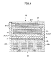
- the composite electronic component of the second embodiment is shown in a perspective view of Fig. 3 and a vertically sectional view of Fig. 4 .
- the reference numeral 20 denotes a composite electronic component of the second embodiment.
- the composite electronic component 20 has a rectangular parallelepiped shape.
- Figs. 3 the composite electronic component 20 has a rectangular parallelepiped shape.
- the composite electronic component 20 has a dielectric body portion 21, a magnetic body portion 22, an intermediate layer 23, a first joint layer 24, a second joint layer 25, a third joint layer 27, and external electrodes 26A to 26H as constituent elements thereof.
- the dielectric body portion 21 and the magnetic body portion 22 have a rectangular parallelepiped shape.
- the intermediate layer 23, the first joint layer 24, and the third joint layer 27 also have a rectangular parallelepiped shape. However, since thickness of these layers is relatively small, it can also be considered that the layers have a plate shape.
- the second joint layer 25 has a plate shape surrounding a circumference of the intermediate layer 23.
- an upper part seen on a paper plane of Fig. 4 is referred to as the "upper side”.
- a lower part is the “lower side”
- a left part is the “left side”
- a right part is the “right side” in the following description.
- the dielectric body portion 21 has a plurality of conductive bodies 21C, and a main body 21B.
- a configuration of the conductive bodies 21C is the same as the configuration of the conductive bodies 11C of the first embodiment, and a configuration of the main body 21B is the same as the configuration of the main body 11B of the first embodiment.
- further description of the conductive bodies 21C and the main body 21B will be omitted.
- the magnetic body portion 22 has a plurality of conductive bodies 22C, and a main body 22B.
- a configuration of the conductive bodies 22C is the same as the configuration of the conductive bodies 12C of the first embodiment, and a configuration of the main body 22B is the same as the configuration of the main body 12B of the first embodiment.
- further description of the conductive bodies 22C and the main body 22B will be omitted.
- the intermediate layer 23 is arranged between the dielectric body portion 21 and the first joint layer 24 and also surrounded by the second joint layer 25.
- Other configuration of the intermediate layer 23 is the same as the configuration of the intermediate layer 13 of the first embodiment. Thus, further description of the intermediate layer 23 will be omitted.
- the first joint layer 24 is arranged between the intermediate layer 23, the second joint layer 25, and the third joint layer 27.
- Part of an upper wall surface of the first joint layer 24 is in contact with an entire lower wall surface of the intermediate layer 23 and an entire lower wall surface of the second joint layer 25, and an entire lower wall surface thereof is in contact with an entire upper wall surface of the third joint layer 27. That is, a peripheral area of the upper wall surface of the first joint layer 24 is in contact with the entire lower wall surface of the second joint layer 25, and an area excluding the peripheral area is in contact with the entire lower wall surface of the intermediate layer 23. End surfaces of the first joint layer 24 are exposed onto wall surfaces of the composite electronic component 20 in contact with the external terminal electrodes 26A to 26H.
- the first joint layer 24 is formed of a material in which a dielectric body material such as a Ba-Ti-Zn-based dielectric body material, glass such as zinc borosilicate glass, and CuO are mixed.
- the second joint layer 25 is arranged between the dielectric body portion 21 and the first joint layer 24 and surrounds the intermediate layer 23.
- Other configuration of the second joint layer 25 is the same as the configuration of the second joint layer 15 of the first embodiment. Thus, further description of the second joint layer 25 will be omitted.
- the third joint layer 27 is arranged between the first joint layer 24 and the magnetic body portion 22.
- the entire upper wall surface of the third joint layer 27 is in contact with the entire lower wall surface of the first joint layer 24, and an entire lower wall surface thereof is in contact with an entire upper wall surface of the main body 22B of the magnetic body portion 22.
- Outer end surfaces of the third joint layer 27 are exposed onto the wall surfaces of the composite electronic component 20 in contact with the external terminal electrodes 26A to 26H.
- the third joint layer 27 is formed of a mixture of a dielectric body material of the first joint layer 24 and a magnetic material of the main body 22B of the magnetic body portion 22. That is, the third joint layer 27 has a composition in a middle of a composition of the first joint layer 24 and a composition of the main body 22B of the magnetic body portion 22.
- the third joint layer 27 having the composition in the middle of the compositions of the first joint layer and the magnetic body portion is arranged between the first joint layer 24 and the magnetic body portion 22 in such a way, the first joint layer 24 and the magnetic body portion 22 can be jointed with a further high joint strength.
- the composite electronic component 20 of the second embodiment is manufactured by assembling the dielectric body portion 21, the magnetic body portion 22, the intermediate layer 23, the first joint layer 24, the second joint layer 25, and the third joint layer 27 in the positional relationship described above so as to produce a laminated body, sintering the laminated body so as to produce a sintered body, and forming the external electrodes 26A to 26H in the sintered body.
- part of a material or an element of the main body 21B of the dielectric body portion 21 (hereinafter, the material and the element are collectively called the "dielectric body material”) is apt to diffuse inside of the magnetic body portion 22.
- the dielectric body material cannot diffuse in the intermediate layer 23.
- diffusion of the dielectric body material inside of the magnetic body portion 22 via the first joint layer 24 and the third joint layer 27 is suppressed.
- part of a material or an element of the main body 22B of the magnetic body portion 22 (hereinafter, the material and the element are collectively called the "magnetic body material”) is apt to diffuse inside of the dielectric body portion 21.
- the magnetic body material cannot diffuse in the intermediate layer 23.
- diffusion of the magnetic body material inside of the dielectric body portion 21 via the third joint layer 27 and the first joint layer 24 is suppressed.
- the intermediate layer 23 formed of the same material or the same element as the material or the element of the conductive bodies 21C of the dielectric body portion 21 is arranged between the dielectric body portion 21 and the magnetic body portion 22, or the intermediate layer 23 formed of the same material or the same element as the material or the element of the conductive bodies 22C of the magnetic body portion 22 is arranged between the dielectric body portion 21 and the magnetic body portion 22; a sufficiently high joint strength is ensured between the dielectric body portion 21 and the magnetic body portion 22, and sufficiently enhanced electric properties of the dielectric body portion 21 and the magnetic body portion 22 are ensured.
- the conductive bodies 21C of the dielectric body portion 21 is exposed onto a lower wall surface of the dielectric body portion 21 (that is, the lower wall surface of the dielectric body portion 21 is formed by a lower wall surface of the conductive body 21C), and the first joint layer 24, the third joint layer 27, and the magnetic body portion 22 are provided in a manner that the upper wall surface of the first joint layer 24 is in contact with the lower wall surface of the conductive body 21C, the upper wall surface of the third joint layer 27 is in contact with the lower wall surface of the first joint layer 24, and an upper wall surface of the magnetic body portion 22 is in contact with the lower wall surface of the third joint layer 27; the conductive body 21C exposed onto the lower wall surface of the dielectric body portion 21 serves as the intermediate layer 23, which ensures a sufficiently high joint strength between the dielectric body portion 21 and the magnetic body portion 22 and sufficiently enhanced electric properties of the dielectric body portion 21 and the magnetic body portion
- the intermediate layer 23 serves to suppress the dielectric body material (that is, the material of the main body 21B of the dielectric body portion 21) from diffusing inside of the magnetic body portion 22, and suppress the magnetic body material (that is, the material of the main body 22B of the magnetic body portion 22) from diffusing inside of the dielectric body portion 21.
- the intermediate layer 23 serves as a diffusion suppressing layer.
- the intermediate layer 23 is a metal material having a plastic deformation property, and thus the intermediate layer also serves to absorb a difference between a contraction rate of the dielectric body portion 21 and a contraction rate of the magnetic body portion 22 when the sintered body is cooled after sintering the above laminated body, which suppresses cracking in the cooled sintered body.
- the first joint layer 24, the second joint layer 25, and the third joint layer 27 it is preferable for the first joint layer 24, the second joint layer 25, and the third joint layer 27 to have a thermal expansion coefficient which is in a middle between the dielectric body portion 21 and the magnetic body portion 22 so as to absorb the difference between the contraction rates of both the portions.
- the material of the conductive bodies 21C of the dielectric body portion 21 is used, or the material of the conductive bodies 22C of the magnetic body portion 22 is used.
- a metal material other than the material of the conductive bodies 21C of the dielectric body portion 21 or the conductive bodies 22C of the magnetic body portion 22 may be used, or the material of the conductive bodies 21C of the dielectric body portion 21 and a material other than the material may be used, or the material of the conductive bodies 22C of the magnetic body portion 22 and a material other than the material may be used.
- the dielectric body portion 11 and the magnetic body portion 12 may be produced by a known tape laminating method or produced by a gel casting method.
- the gel casting method is a ceramic powder molding method of pouring slurry containing ceramic powder into a mold and hardening or gelatinizing the slurry in the mold, so as to produce a molded body (compact) without flowability. Since a dispersion medium is evaporated after the slurry loses the flowability, the gel casting method has a characteristic that molding contraction is small. Therefore, when the gel casting method is used at the time of burying a thick conductive body into a ceramic compact, a compact can be obtained without a damage such as cracking due to molding contraction.
- the slurry used in production of the ceramic compact by the gel casting method is prepared by adding a hardening agent, a gelatinizing agent, and the like to the dispersion medium in which the ceramic powder is dispersed.
- the hardening agent (gelatinizing agent) contains a precursor of a resin hardener (resin gelatinizer), and a hardening initiator/accelerator (gelatinization initiator/accelerator) for initiating or accelerating hardening (gelatinization) of the precursor of the resin hardener.
- the dispersion medium is selected from water, a non-polar organic solvent, a polar organic solvent, and the like.
- the organic solvent selected as the dispersion medium includes lower alcohols such as methanol, ethanol, and isopropyl alcohol, higher alcohol, acetone, hexane, benzene, toluene, and diols such as ethylene glycol, triols such as glycerin, polybasic acid ester such as glutaric dimethyl, esters containing two or more ester groups such as triacetin, polyester compound such as polycarboxylate ester, phosphate ester, amine condensate, non-ionic specific amide compound, and the like.
- the dispersion medium may be any of a pure substance and a mixture.
- a resin of the resin hardener is selected from an epoxy resin, an acrylic resin, a urethane resin, and the like.
- the resin is selected from substances having a high compatibility with the dispersion medium and low reactivity to the dispersion medium.
- an epoxy resin a polymer containing, as constituent monomer(s), ethylene glycol diglycidyl ether, polyethylene glycol diglycidyl ether, propylene glycol diglycidyl ether, polypropylene glycol, glycerol diglycidyl ether, and the like is selected.
- acrylic resin a polymer containing, as constituent monomer(s), acrylamide, methacrylic acid, N-hydroxymethyl acrylamide, acrylate ammonium salt, and the like is selected.
- urethane resin a polymer containing, as constituent monomers, MDI (4, 4-diphenylmethane diisocyanate) isocyanate, HDI (hexamethylene diisocyanate) isocyanate, TDI (tolylenediisocyanate) isocyanate, IPDI (isophorone diisocyanate) isocyanate, isothiocyanate, and the like is selected.
- the hardening initiator/accelerator is selected in consideration with reactivity between the hardening initiator/accelerator and the precursor of the resin hardener.
- the hardening initiator/accelerator is selected from polyalkylene polyamine of a polymer of tetramethylethylenediamine, triethylenediamine, hexanediamine, ethylenediamine, and the like, perazines such as 1-(2-aminoethyl)piperazine, polyether amine such as polyoxypropylene diamine, N, N'-methylenebisacrylamide, 6-dimethylamino-1-hexanol, ammonium persulfate, hydrogen peroxide, and the like.
- a mixture of triacetin and dimethyl glutarate is selected as the dispersion medium, and polymethylenepolyphenyl polyisocyanate and ethylene glycol are selected as the gelatinizing agent.
- a dispersant such as a carboxylic acid copolymer and an acrylic acid copolymer may further be added to the dispersion medium in order to improve a dispersion property, or a catalyzer such as 6-dimethylamino-1-hexanol may further be added in order to facilitate hardening (gelatinization) reaction.
- the gel casting method has a merit that a contained amount of the ceramic powder of a dielectric body and a magnetic body to be contained in the slurry can be adjusted in a wide range. Since sintering contraction amounts at the time of sintering can be controlled by means of the contained amount of the ceramic powder in the slurry, by producing one or both of the dielectric body portion 11 and the magnetic body portion 12 by the gel casting method, the contraction amounts at the time of sintering can be easily matched with each other. Thus, when being sintered, those portions can be suppressed from being detached from each other, so that it is advantageous for integrating those portions.
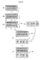
- a manufacturing procedure of the composite electronic component of the first embodiment will be described.
- the manufacturing procedure is shown in Fig. 5 .
- the dielectric body portion 11 is prepared, and the intermediate layer 13 is provided in a predetermined area of the lower wall surface of the dielectric body portion 11 by printing.
- the second joint layer 15 is provided in a predetermined area of the lower wall surface of the dielectric body portion 11 by printing.
- the first joint layer 14 is provided onto the entire lower wall surface of the intermediate layer 13 and the entire lower wall surface of the second joint layer 15 by printing. Thereby, a partial laminated body 10A is produced.
- the magnetic body portion 12 is prepared.
- the partial laminated body 10A and the magnetic body portion 12 are assembled to each other in a manner that an entire lower wall surface of the partial laminated body 10A (more specifically, the entire lower wall surface of the first joint layer 14) and the entire upper wall surface of the magnetic body portion 12 are in contact with each other.
- a laminated body 10B is produced as shown in Fig. 5(F) .
- the laminated body 10B is cut into individual laminated bodies to each form one final composite electronic component 10.
- the composite electronic component 10 is manufactured.
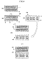
- the manufacturing procedure is shown in Fig. 6 .
- the dielectric body portion 11 is prepared, and the intermediate layer 13 is provided in a predetermined area of the lower wall surface of the dielectric body portion 11 by printing.
- the second joint layer 15 is provided in a predetermined area of the lower wall surface of the dielectric body portion 11 by printing.
- a partial laminated body 10A is produced.
- the magnetic body portion 12 is prepared, and the first joint layer 14 is provided onto the entire upper wall surface of the magnetic body portion 12 by printing.
- a partial laminated body 10B is produced.
- the partial laminated bodies 10A, 10B are assembled to each other in a manner that an entire lower wall surface of the partial laminated body 10A (more specifically, the entire lower wall surface of the intermediate layer 13 and the entire lower wall surface of the second joint layer 15) and an entire upper wall surface of the partial laminated body 10B (more specifically, the entire upper wall surface of the first joint layer 14) are in contact with each other.
- a laminated body 10C is produced as shown in Fig. 6(E) .
- the laminated body 10C is cut into individual laminated bodies to each form one final composite electronic component 10.
- the composite electronic component 10 is manufactured.
- FIG. 7 The manufacturing procedure is shown in Fig. 7 .
- the first joint layer 14 is prepared.
- the intermediate layer 13 is provided in a predetermined area of the upper wall surface of the first joint layer 14 by printing.
- the second joint layer 15 is provided in a predetermined area of the upper wall surface of the first joint layer 14 by printing.
- a partial laminated body 10A is produced.
- the dielectric body portion 11 is prepared. Meanwhile, as shown in Fig.
- the magnetic body portion 12 is prepared. As shown in Fig. 7(F) , the partial laminated body 10A, the dielectric body portion 11, and the magnetic body portion 12 are assembled to each other in a manner that an entire upper wall surface of the partial laminated body 10A (more specifically, the entire upper wall surface of the intermediate layer 13 and the entire upper wall surface of the second joint layer 15) and the entire lower wall surface of the dielectric body portion 11 are in contact with each other, and in a manner that an entire lower wall surface of the partial laminated body 10A (more specifically, the entire lower wall surface of the first joint layer 14) and the entire upper wall surface of the magnetic body portion 12 are in contact with each other.
- a laminated body 10B is produced as shown in Fig. 7(G) .
- the laminated body 10B is cut into individual laminated bodies to each form one final composite electronic component 10.
- the composite electronic component 10 is manufactured.
- Fig. 8 The manufacturing procedure is shown in Fig. 8 .
- the dielectric body portion 21 is prepared, and the intermediate layer 23 is provided in a predetermined area of the lower wall surface of the dielectric body portion 21 by printing.
- the second joint layer 25 is provided in a predetermined area of the lower wall surface of the dielectric body portion 21 by printing.
- the first joint layer 24 is provided onto the entire lower wall surface of the intermediate layer 23 and the entire lower wall surface of the second joint layer 25 by printing.
- Fig. 8(A) the dielectric body portion 21 is prepared, and the intermediate layer 23 is provided in a predetermined area of the lower wall surface of the dielectric body portion 21 by printing.
- the second joint layer 25 is provided in a predetermined area of the lower wall surface of the dielectric body portion 21 by printing.
- the first joint layer 24 is provided onto the entire lower wall surface of the intermediate layer 23 and the entire lower wall surface of the second joint layer 25 by printing.
- the third joint layer 27 is provided onto the entire lower wall surface of the first joint layer 24 by printing. Thereby, a partial laminated body 20A is produced. Meanwhile, as shown in Fig. 8(E) , the magnetic body portion 22 is prepared. As shown in Fig. 8(F) , the partial laminated body 20A and the magnetic body portion 22 are assembled to each other in a manner that an entire lower wall surface of the partial laminated body 20A (more specifically, the entire lower wall surface of the third joint layer 27) and the entire upper wall surface of the magnetic body portion 22 are in contact with each other. By pressing with uniaxial press or CIP (Cold Isostatic Press), a laminated body 20B is produced as shown in Fig. 8(G) . Next, the laminated body 20B is cut into individual laminated bodies to each form one final composite electronic component 20. By sintering and then cooling the individual laminated bodies, and providing the external electrodes 26A to 26H, the composite electronic component 20 is manufactured.
- CIP Cold Isostatic Press
- Fig. 9 The manufacturing procedure is shown in Fig. 9 .
- the dielectric body portion 21 is prepared, and the intermediate layer 23 is provided in a predetermined area of the lower wall surface of the dielectric body portion 21 by printing.
- the second joint layer 25 is provided in a predetermined area of the lower wall surface of the dielectric body portion 21 by printing.
- a partial laminated body 20A is produced.
- the magnetic body portion 22 is prepared, and the third joint layer 27 is provided onto the entire upper wall surface of the magnetic body portion 22 by printing.
- Fig. 9(C) the third joint layer 27 is provided onto the entire upper wall surface of the magnetic body portion 22 by printing.
- the first joint layer 24 is provided onto the entire upper wall surface of the third joint layer 27 by printing. Thereby, a partial laminated body 20B is produced.
- the partial laminated bodies 20A, 20B are assembled to each other in a manner that an entire lower wall surface of the partial laminated body 20A (more specifically, the entire lower wall surface of the intermediate layer 23 and the entire lower wall surface of the second joint layer 25) and an entire upper wall surface of the partial laminated body 20B (more specifically, the entire upper wall surface of the first joint layer 24) are in contact with each other.
- a laminated body 20C is produced as shown in Fig. 9(F) .
- the laminated body 20C is cut into individual laminated bodies to each form one final composite electronic component 20.
- the composite electronic component 20 is manufactured.
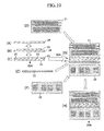
- FIG. 10 The manufacturing procedure is shown in Fig. 10 .
- the first joint layer 24 is prepared.
- the intermediate layer 23 is provided in a predetermined area of the upper wall surface of the first joint layer 24 by printing.
- the second joint layer 25 is provided in a predetermined area of the upper wall surface of the first joint layer 24 by printing.
- a partial laminated body 20A is produced.
- the dielectric body portion 21 is prepared. Meanwhile, as shown in Fig.
- the third joint layer 27 is prepared.
- the magnetic body portion 22 is prepared.
- the partial laminated body 20A, the dielectric body portion 21, the third joint layer 27, and the magnetic body portion 22 are assembled to each other in a manner that an entire upper wall surface of the partial laminated body 20A (more specifically, the entire upper wall surface of the intermediate layer 23 and the entire upper wall surface of the second joint layer 25) and the entire lower wall surface of the dielectric body portion 21 are in contact with each other, an entire lower wall surface of the partial laminated body 20A (more specifically, the entire lower wall surface of the first joint layer 24) and the entire upper wall surface of the third joint layer 27 are in contact with each other, and the entire lower wall surface of the third joint layer 27 and the entire upper wall surface of the magnetic body portion 22 are in contact with each other.
- a laminated body 20B is produced as shown in Fig. 10(H) .
- the laminated body 20B is cut into individual laminated bodies to each form one final composite electronic component 20.
- the composite electronic component 20 is manufactured.
Landscapes
- Engineering & Computer Science (AREA)
- Power Engineering (AREA)
- Microelectronics & Electronic Packaging (AREA)
- Manufacturing & Machinery (AREA)
- Coils Or Transformers For Communication (AREA)
- Fixed Capacitors And Capacitor Manufacturing Machines (AREA)
Abstract
Description
- The present invention relates to a composite electronic component.
- Patent Document 1 describes a LC composite component serving as a composite electronic component. The LC composite component is formed by jointing a part made of a dielectric material (hereinafter, this part is called the "dielectric body portion") and a part made of a magnetic material (hereinafter, this part is called the "magnetic body portion") via a part made of a specific material (hereinafter, this part is called the "intermediate part"). In the LC composite component, plural pairs of electrodes including conductive bodies are provided inside of the dielectric body portion, the dielectric body portion functions as a capacitor, a coil including a conductive body is formed inside of the magnetic body portion, and the magnetic body portion functions as an inductor.
- The dielectric body portion of the composite electronic component described in Patent Document 1 is formed of a material of crystallized glass containing SiO2, Al2O3, CaO, and the like, the material containing Ni-Cu-Zn ferrite. Meanwhile, the magnetic body portion of the composite electronic component described in Patent Document 1 is formed of magnetic ferrite powder. Therefore, a thermal expansion coefficient of the dielectric body portion and a thermal expansion coefficient of the magnetic body portion are different from each other. Therefore, if the dielectric body portion and the magnetic body portion are directly jointed to each other without any intermediate part, the jointed dielectric and magnetic body portions are sintered, and the sintered dielectric and magnetic body portions are cooled, there is a possibility that cracking is generated in a joint area between the dielectric body portion and the magnetic body portion at this cooling stage, and there is a possibility that the dielectric body portion and the magnetic body portion are detached from each other. Thus, in Patent Document 1, glass is used as the material of the intermediate part, which realizes a thermal expansion coefficient of the intermediate part so as to absorb a difference between contraction of the dielectric body portion and contraction of the magnetic body portion at the cooling stage of the sintered dielectric and magnetic body portions.
- A composite electronic component is also described in Patent Document 2. The composite electronic component is also formed by jointing a dielectric body portion and a magnetic body portion via an intermediate part. In the composite electronic component as well, plural pairs of electrodes including conductive bodies are provided inside of the dielectric body portion, the dielectric body portion functions as a capacitor, a coil including a conductive body is formed inside of the magnetic body portion, and the magnetic body portion functions as an inductor. The dielectric body portion of the composite electronic component described in Patent Document 2 is formed of ceramic such as TiO2 and Ba3O4. Meanwhile, the magnetic body portion of the composite electronic component described in Patent Document 2 is formed of magnetic oxide ferrite. Therefore, as well as the composite electronic component described in Patent Document 1, a thermal expansion coefficient of the dielectric body portion and a thermal expansion coefficient of the magnetic body portion are different from each other in the composite electronic component described in Patent Document 2. Thus, in Patent Document 2, a material in which one of glass, alumina, and ferrite is mixed with a material of the dielectric body portion is used as a material of the intermediate part, which realizes a thermal expansion coefficient of the intermediate part so as to absorb a difference between contraction of the dielectric body portion and contraction of the magnetic body portion at the cooling stage of the sintered dielectric and magnetic body portions.
- A composite electronic component is also described in Patent Document 3 (
JP4020886B - In such a way, in Patent Documents 1 to 3, for jointing the dielectric and magnetic body portions having different thermal expansion coefficients from each other, the dielectric body portion and the magnetic body portion are jointed via the intermediate part having the thermal expansion coefficient so as to absorb the difference between the contraction of the dielectric body portion and the contraction of the magnetic body portion at the cooling stage of the sintered dielectric and magnetic body portions, so that the dielectric body portion and the magnetic body portion are favorably jointed.
- Patent Literature:
- Patent Document 1;
JP1983(S58)-172804A - Patent Document 2;
JP1984(S59)-33247B - Patent Document 3;
JP4020886B - In the composite electronic component formed by jointing the dielectric body portion and the magnetic body portion via the intermediate part as described above, when the composite electronic component was sintered, there is sometimes a case where part of the material of the dielectric body portion diffuses inside of the magnetic body portion, part of the material of the magnetic body portion diffuses inside of the dielectric body portion, or part of the material of the intermediate part diffuses inside of the dielectric body portion or inside of the magnetic body portion. Such diffusion may result in an insufficient joint strength between the dielectric body portion and the magnetic body portion via the intermediate part. When part of the material of the dielectric body portion or the intermediate part diffuses inside of the magnetic body portion, a property of the magnetic body portion may be deteriorated. When part of the material of the magnetic body portion or the intermediate part diffuses inside of the dielectric body portion, a property of the dielectric body portion may be deteriorated.
- In such a composite electronic component described in Patent Documents 1 and 2 in which there is no countermeasure for suppressing the diffusion of the materials between the dielectric body portion, the magnetic body portion, and the intermediate part, there is a high possibility that the joint strength between the dielectric body portion and the magnetic body portion is not sufficiently ensured as described above. There is also a high possibility that the properties of the dielectric body portion and the magnetic body portion are deteriorated.
- Meanwhile, in the composite electric component described in Patent Document 3, by increasing a contained amount of Zn in the intermediate part more than a contained amount of Zn in the magnetic body portion, Zn contained in the magnetic body portion is suppressed from diffusing in the dielectric body portion. That is, according to this, since the contained amount of Zn in the intermediate part placed between the magnetic body portion and the dielectric body portion exceeds the contained amount in the magnetic body portion, Zn contained in the magnetic body portion is suppressed from diffusing in the dielectric body portion, by means of the intermediate part. However, the material to be suppressed from diffusing by the intermediate part is limited to Zn. On the other hand, the dielectric body portion and the magnetic body portion contain materials or elements other than Zn, and such materials or elements cannot be suppressed from diffusing by the intermediate part. Diffusion of such materials or elements between the dielectric body portion and the magnetic body portion may also result in an insufficient joint strength between the dielectric body portion and the magnetic body portion, or deteriorated properties of the dielectric body portion and the magnetic body portion.
- An object of the present invention is, in a composite electronic component having a dielectric body portion inside of which a conductive body is provided, and a magnetic body portion inside of which a conductive body is provided, to suppress a material or an element of a part surrounding the conductive body of the dielectric body portion from diffusing inside of the magnetic body portion, or to suppress a material or an element of a part surrounding the conductive body of the magnetic body portion from diffusing inside of the dielectric body portion.
- The invention of the present application relates to a composite electronic component having a dielectric body portion inside of which a conductive body is provided, and a magnetic body portion inside of which a conductive body is provided. In the present invention, a layer made of a metal material is arranged between the dielectric body portion and the magnetic body portion as an intermediate layer.
- According to this, at the time of sintering the composite electronic component of the present invention, even when a material or an element of a part surrounding the conductive body of the dielectric body portion (hereinafter, the material and the element are collectively called the "dielectric body material") diffuses inside of the magnetic body portion, such diffusion is suppressed by the above intermediate layer. That is, the dielectric body material is suppressed from diffusing inside of the magnetic body portion. At the time of sintering the composite electronic component of the present invention, even when a material or an element of a part surrounding the conductive body of the magnetic body portion (hereinafter, the material and the element are collectively called the "magnetic body material") diffuses inside of the dielectric body portion, such diffusion is suppressed by the above intermediate layer. That is, the magnetic body material is suppressed from diffusing inside of the dielectric body portion. This further ensures a sufficiently high joint strength between the dielectric body portion and the magnetic body portion, and sufficiently enhanced properties of the dielectric body portion and the magnetic body portion.
- In the above invention, the intermediate layer is made of the same material or the same element as a material or an element of the conductive body of the dielectric body portion, or the same material or the same element as a material or an element of the conductive body of the magnetic body portion.
- According to this, the intermediate layer is formed of the same material or the same element as the material or the element of the conductive body of the dielectric body portion, or the same material or the same element as the material or the element of the conductive body of the magnetic body portion; which facilitates manufacturing of the composite electronic component of the present invention.
- In the above invention, the conductive body of the dielectric body portion and the conductive body of the magnetic body portion are formed of the same material or the same element.
- According to this, the material or the element of the intermediate layer is the same as the material or the element of the conductive body of the dielectric body portion, and the material or the element of the conductive body of the magnetic body portion; which facilitates manufacturing of the composite electronic component of the present invention.
- In the above invention, a layer formed of a material having a higher joint strength to the dielectric body portion and the intermediate layer than a predetermined strength is arranged between the dielectric body portion and the intermediate layer as a joint layer, or a layer formed of a material having a higher joint strength to the magnetic body portion and the intermediate layer than a predetermined strength is arranged between the magnetic body portion and the intermediate layer as a joint layer.
- According to this, in the case where the joint layer formed of the material having a higher joint strength to the dielectric body portion and the intermediate layer than a predetermined strength is arranged between the dielectric body portion and the intermediate layer, the joint strength between the joint layer and the dielectric body portion and the intermediate layer is relatively high, even if joint strength between the intermediate layer and the dielectric body portion is low and thus joint strength between the dielectric body portion and the magnetic body portion via the intermediate layer is low; which ensures a relatively high joint strength between the dielectric body portion and the magnetic body portion via the joint layer. Meanwhile, in the case where the joint layer formed of the material having a higher joint strength to the magnetic body portion and the intermediate layer than a predetermined strength is arranged between the dielectric body portion and the magnetic body portion, joint strength between the joint layer and the magnetic body portion and the intermediate layer is relatively high, even if joint strength between the intermediate layer and the magnetic body portion is low and thus the joint strength between the dielectric body portion and the magnetic body portion via the intermediate layer is low; which ensures a relatively high joint strength between the dielectric body portion and the magnetic body portion via the joint layer.
-
-
Fig. 1 is a perspective view of a composite electronic component of a first embodiment. -
Fig. 2 is a vertically sectional view of the composite electronic component of the first embodiment along a plane shown by a one-chain line S ofFig. 1 . -
Fig. 3 is a perspective view of a composite electronic component of a second embodiment. -
Fig. 4 is a vertically sectional view of the composite electronic component of the second embodiment along a plane shown by a one-chain line S ofFig. 3 . -
Fig. 5 is a view showing one example of a manufacturing procedure of the composite electronic component of the first embodiment. -
Fig. 6 is a view showing another example of the manufacturing procedure of the composite electronic component of the first embodiment. -
Fig. 7 is a view showing still another example of the manufacturing procedure of the composite electronic component of the first embodiment. -
Fig. 8 is a view showing one example of a manufacturing procedure of the composite electronic component of the second embodiment. -
Fig. 9 is a view showing another example of the manufacturing procedure of the composite electronic component of the second embodiment. -
Fig. 10 is a view showing still another example of the manufacturing procedure of the composite electronic component of the second embodiment. - Hereinafter, embodiments of a composite electronic component of the present invention will be described. One embodiment of the composite electronic component of the present invention (hereinafter, the "first embodiment") is shown in a perspective view of
Fig. 1 and a vertically sectional view ofFig. 2 . InFigs. 1 and2 , thereference numeral 10 denotes a composite electronic component of the first embodiment. As shown inFig. 1 , the compositeelectronic component 10 has a rectangular parallelepiped shape. As shown inFigs. 1 and2 , the compositeelectronic component 10 has adielectric body portion 11, amagnetic body portion 12, anintermediate layer 13, a firstjoint layer 14, a secondjoint layer 15, andexternal electrodes 16A to 16H as constituent elements thereof. Thedielectric body portion 11 and themagnetic body portion 12 have a rectangular parallelepiped shape. Theintermediate layer 13 and the firstjoint layer 14 also have a rectangular parallelepiped shape, and thickness of these layers is relatively small, it can also be considered that the layers have a plate shape. The secondjoint layer 15 has a plate shape surrounding a circumference of theintermediate layer 13. - Next, the above constituent elements of the composite
electronic component 10 will be described in detail. For the purpose of convenience, an upper part seen on a paper plane ofFig. 2 is referred to as the "upper side". Similarly, a lower part is the "slower side", a left part is the "left side", and a right part is the "right side", in the following description. - As shown in
Fig. 2 , thedielectric body portion 11 has a plurality of conductive bodies 11C, and amain body 11B. Themain body 11B surrounds the conductive bodies 11C. In other words, the conductive bodies 11C are arranged inside of themain body 11B, that is, inside of thedielectric body portion 11. The conductive bodies 11C have a plate shape. The conductive bodies 11C are arranged in parallel to each other, and plural pairs of the conductive bodies are connected to predetermined external terminals, respectively. Therefore, thedielectric body portion 11 functions as a capacitor. That is, a plurality of capacitors is formed inside of thedielectric body portion 11, and the capacitors are connected to the predetermined external terminals, respectively. - The
main body 11B of thedielectric body portion 11 is formed of a dielectric body material such as a BaTiO3-based dielectric body material and a TiO2-based dielectric body material. The conductive bodies 11C of thedielectric body portion 11 are formed of a metal material such as Ag and Cu, that is, a conductive body material. - As shown in
Fig. 2 , themagnetic body portion 12 has a plurality of conductive bodies 12C, and amain body 12B. Themain body 12B surrounds the conductive bodies 12C. In other words, the conductive bodies 12C are arranged inside of themain body 12B, that is, inside of themagnetic body portion 12. The conductive bodies 12C have a coil shape. In the conductive bodies 12C, ends of the coils are exposed onto wall surfaces of themagnetic body portion 12. In one example, one ends of the conductive bodies 12C forming the coils are connected to theelectrode 16A or 16C, and the other ends are connected to theelectrode magnetic body portion 12 functions as an inductor. That is, a plurality of inductors is formed inside of themagnetic body portion 12, and the inductors are respectively connected to predetermined external terminals. - The
main body 12B of themagnetic body portion 12 is formed of a magnetic material such as a Ni-Cu-Zn-based ferrite material and a Mn-Zn-based ferrite material. The conductive bodies 12C of themagnetic body portion 12 are formed of a metal material such as Ag and Cu, that is, a conductive body material. - As shown in
Fig. 2 , theintermediate layer 13 is arranged between thedielectric body portion 11 and the firstjoint layer 14 and surrounded by the secondjoint layer 15. InFig. 2 , a part of the secondjoint layer 15 on the left side of theintermediate layer 13 is referred to as the "left part of the second joint layer" and denoted by thereference numeral 15L, and a part of the secondjoint layer 15 on the right side of theintermediate layer 13 is referred to as the "right part of the second joint layer" and denoted by thereference numeral 15R. When seen inFig. 2 , it can also be considered that theintermediate layer 13 is arranged between thedielectric body portion 11, the firstjoint layer 14, theleft part 15L of the second joint layer, and theright part 15R of the second joint layer. An entire upper wall surface of theintermediate layer 13 is in contact with part of a lower wall surface of themain body 11B of thedielectric body portion 11, an entire lower wall surface thereof is in contact with part of an upper wall surface of the firstjoint layer 14, and entire end surfaces thereof are in contact with entire inner end surfaces of the secondjoint layer 15. That is, the upper wall surface of theintermediate layer 13 is in contact with only an area of the lower wall surface of themain body 11B of thedielectric body portion 11 excluding an area close to wall surfaces of thedielectric body portion 11. The lower wall surface of theintermediate layer 13 is in contact with only an area of the upper wall surface of the firstjoint layer 14 excluding an area close to the wall surfaces of thedielectric body portion 11. Since the entire outer end surfaces of theintermediate layer 13 are in contact with the inner end surfaces of the secondjoint layer 15, theintermediate layer 13 is not exposed onto wall surfaces of the compositeelectronic component 10 in no contact with the externalterminal electrodes 16A to 16H. Theintermediate layer 13 is formed of a metal material such as Ag and Cu. - As shown in
Fig. 2 , the firstjoint layer 14 is arranged between theintermediate layer 13, the secondjoint layer 15, and themagnetic body portion 12. Part of the upper wall surface of the firstjoint layer 14 is in contact with the entire lower wall surface of theintermediate layer 13 and an entire lower wall surface of the secondjoint layer 15, and an entire lower wall surface thereof is in contact with an entire upper wall surface of themain body 12B of themagnetic body portion 12. That is, a peripheral area of the upper wall surface of the firstjoint layer 14 is in contact with the entire lower wall surface of the secondjoint layer 15, and an area excluding the peripheral area is in contact with the entire lower wall surface of theintermediate layer 13. End surfaces of the firstjoint layer 14 are exposed onto the wall surfaces of the compositeelectronic component 10 in contact with the externalterminal electrodes 16A to 16H. The firstjoint layer 14 is formed of a material in which a dielectric body material such as a Ba-Ti-Zn-based dielectric body material, glass such as zinc borosilicate glass, and CuO are mixed. - As shown in
Fig. 2 , the secondjoint layer 15 is arranged between thedielectric body portion 11 and the firstjoint layer 14 and surrounds theintermediate layer 13. An entire upper wall surface of the secondjoint layer 15 is in contact with part of the lower wall surface of themain body 11B of thedielectric body portion 11, the entire inner end surfaces thereof are in contact with the entire outer end surfaces of theintermediate layer 13, and the entire lower wall surface thereof is in contact with part of the upper wall surface of the firstjoint layer 14. Outer end surfaces of the secondjoint layer 15 are exposed onto the wall surfaces of the compositeelectronic component 10 in contact with the externalterminal electrodes 16A to 16H. The secondjoint layer 15 is formed of a material in which a dielectric body material such as a Ba-Ti-Zn-based dielectric body material, glass such as zinc borosilicate glass, and CuO are mixed. That is, the secondjoint layer 15 is formed of the material having the same composition as the material of the firstjoint layer 14. However, a ratio of the dielectric body material, a ratio of glass, and a ratio of CuO in the material of the secondjoint layer 15 may be respectively the same as corresponding ratios in the material of the firstjoint layer 14, or the ratio of glass and the ratio of CuO in the material of the secondjoint layer 15 may be respectively larger than the corresponding ratios in the material of the firstjoint layer 14. - The composite
electronic component 10 of the first embodiment is manufactured by assembling thedielectric body portion 11, themagnetic body portion 12, theintermediate layer 13, the firstjoint layer 14, and the secondjoint layer 15 in the positional relationship described above so as to produce a laminated body, sintering the laminated body so as to produce a sintered body, and forming theexternal electrodes 16A to 16H in the sintered body. - During sintering of the above laminated body, part of a material or an element of the
main body 11B of the dielectric body portion 11 (hereinafter, the material and the element are collectively called the "dielectric body material") is apt to diffuse inside of themagnetic body portion 12. Without theintermediate layer 13, the dielectric body material diffuses inside of themagnetic body portion 12 through the firstjoint layer 14. Then, the diffused material lowers joint strength between the firstjoint layer 14 and themagnetic body portion 12 in the finally manufactured compositeelectronic component 10, and also lowers an electric property of themagnetic body portion 12 in the finally manufactured compositeelectronic component 10. Further, a composition of thedielectric body portion 11 is also changed by element diffusion, and thus a sintering property and an electric property of thedielectric body portion 11 are also deteriorated. In an experiment in which, without the intermediate layer 13 (thus without the secondjoint layer 15 as well), only the firstjoint layer 14 is arranged between thedielectric body portion 11 and themagnetic body portion 12 to sinter a laminated body including thedielectric body portion 11, themagnetic body portion 12, and the firstjoint layer 14; a large number of pores were found in both themagnetic body portion 12 and the firstjoint layer 14, the joint strength between the firstjoint layer 14 and themagnetic body portion 12 was low, and the electric properties of thedielectric body portion 11 and themagnetic body portion 12 were deteriorated. It is presumed that a large number of pores were found in such a way, because the dielectric body material diffused inside of the firstjoint layer 14 and themagnetic body portion 12, which results in an insufficient sintering of the material of the firstjoint layer 14 and a material of themain body 12B of themagnetic body portion 12. - However, in the first embodiment, the
intermediate layer 13 is provided, and theintermediate layer 13 is formed of a metal material. That is, theintermediate layer 13 has a structure of metal bond, and thus the dielectric body material cannot diffuse in theintermediate layer 13. As a result, diffusion of the dielectric body material inside of themagnetic body portion 12 via the firstjoint layer 14 is suppressed. Therefore, a sufficiently high joint strength is ensured between the firstjoint layer 14 and themagnetic body portion 12 in the finally manufactured composite electronic component 10 (and eventually, joint strength between thedielectric body portion 11 and the magnetic body portion 12), and sufficiently enhanced electric properties of thedielectric body portion 11 and themagnetic body portion 12 are ensured. In an experiment in which the laminated body including thedielectric body portion 11, themagnetic body portion 12, the firstjoint layer 14, the secondjoint layer 15, and theintermediate layer 13 was sintered according to the first embodiment, few pores were found in themagnetic body portion 12 and the firstjoint layer 14, the joint strength between the firstjoint layer 14 and themagnetic body portion 12 was high, and the electric properties of thedielectric body portion 11 and themagnetic body portion 12 were enhanced. - Meanwhile, during sintering of the above laminated body, part of the material or an element of the
main body 12B of the magnetic body portion 12 (hereinafter, the material and the element are collectively called the "magnetic body material") is apt to diffuse inside of thedielectric body portion 11. Without theintermediate layer 13, the magnetic body material diffuses inside of thedielectric body portion 11 through the firstjoint layer 14. Then, the diffused magnetic body material lowers joint strength between the firstjoint layer 14 and thedielectric body portion 11 in the finally manufactured composite electronic component 10 (without theintermediate layer 13, the secondjoint layer 15 is not provided as well, and thus the upper wall surface of the firstjoint layer 14 is in direct contact with a lower wall surface of the dielectric body portion 11), and also lowers the electric property of thedielectric body portion 11 in the finally manufactured compositeelectronic component 10. Further, a composition of themagnetic body portion 12 is also changed by element diffusion, so that a sintering property and the electric property of themagnetic body portion 12 are also deteriorated. In an experiment in which ,without the intermediate layer 13 (thus without the secondjoint layer 15 as well), only the firstjoint layer 14 is arranged between thedielectric body portion 11 and themagnetic body portion 12 to sinter a laminated body including thedielectric body portion 11, themagnetic body portion 12, and the firstjoint layer 14; a large number of pores were found both in thedielectric body portion 11 and the firstjoint layer 14, the joint strength between the firstjoint layer 14 and thedielectric body portion 11 was low, and the electric properties of thedielectric body portion 11 and themagnetic body portion 12 were deteriorated. It is presumed that a large number of pores were found in such a way, because the magnetic body material diffused inside of the firstjoint layer 14 and thedielectric body portion 11, which results in an insufficient sintering of the material of the firstjoint layer 14 and the material of themain body 11B of thedielectric body portion 11. - However, in the first embodiment, the
intermediate layer 13 is provided, and theintermediate layer 13 is formed of a metal material. That is, theintermediate layer 13 has a structure of metal bond, and thus the magnetic body material cannot diffuse in theintermediate layer 13. As a result, diffusion of the magnetic body material inside of thedielectric body portion 11 via the firstjoint layer 14 is suppressed. Therefore, a sufficiently high joint strength is ensured between the firstjoint layer 14 and thedielectric body portion 11 via theintermediate layer 13 in the finally manufactured composite electronic component 10 (and eventually, the joint strength between themagnetic body portion 12 and the dielectric body portion 11), and sufficiently enhanced electric properties of thedielectric body portion 11 and themagnetic body portion 12 are ensured. In an experiment in which the laminated body including thedielectric body portion 11, themagnetic body portion 12, the firstjoint layer 14, the secondjoint layer 15, and theintermediate layer 13 was sintered according to the first embodiment, few pores were found in thedielectric body portion 11 and the firstjoint layer 14, joint strength between the firstjoint layer 14 and theintermediate layer 13 and joint strength between theintermediate layer 13 and thedielectric body portion 11 were high, and the electric properties of thedielectric body portion 11 and themagnetic body portion 12 were enhanced. - Since the material of the conductive bodies 11C of the dielectric body portion 11 (that is, the conductive body material of the dielectric body portion) and the material of the conductive bodies 12C of the magnetic body portion 12 (that is, the conductive body material of the magnetic body portion) are the same in the first embodiment, the material of the
intermediate layer 13 is the same as both the conductive body material of the dielectric body portion and the conductive body material of the magnetic body portion. However, the thought included in the first embodiment can also be applied to the case where the conductive body material of the dielectric body portion and the conductive body material of the magnetic body portion are different from each other, to obtain a certain effect. In detail, in the case where the conductive body material of the dielectric body portion and the conductive body material of the magnetic body portion are different from each other, theintermediate layer 13 may be formed of the same material as the conductive body material of the dielectric body portion, or theintermediate layer 13 may be formed of the same material as the conductive body material of the magnetic body portion. - In the case where at least one of the material of the
main body 11B of thedielectric body portion 11, the material of the conductive bodies 11C of thedielectric body portion 11, the material of themain body 12B of themagnetic body portion 12, the material of the conductive bodies 12C of themagnetic body portion 12, and the material of the firstjoint layer 14 is different from the materials of the first embodiment, the thought included in the first embodiment can be applied to obtain a certain effect. In this case, not only a certain effect can be obtained in the joint strength between thedielectric body portion 11 and themagnetic body portion 12 and the electric properties of thedielectric body portion 11 and themagnetic body portion 12, but also a certain effect may also be obtained in properties other than the electric properties of thedielectric body portion 11 and themagnetic body portion 12. - Although it may depend on the material of the
main body 11B of thedielectric body portion 11, the material of the conductive bodies 11C of thedielectric body portion 11, the material of themain body 12B of themagnetic body portion 12, the material of the conductive bodies 12C of themagnetic body portion 12, and the material of the firstjoint layer 14, in the case where a positional relationship between theintermediate layer 13 and the firstjoint layer 14 is opposite to the positional relationship of the first embodiment, the thought included in the first embodiment can be applied to obtain a certain effect. That is, in the case where the firstjoint layer 14 is arranged between thedielectric body portion 11, theintermediate layer 13, as well as the secondjoint layer 15, and theintermediate layer 13 is arranged between the firstjoint layer 14 and themagnetic body portion 12 and surrounded by the secondjoint layer 15, the thought included in the first embodiment can be applied to obtain a certain effect. - In the case where another joint layer is arranged between the first
joint layer 14 and themagnetic body portion 12, the thought included in the first embodiment is applied, and thereby, a certain effect can also be obtained. - Although it may depend on the material of the
main body 11B of thedielectric body portion 11, the material of the conductive bodies 11C of thedielectric body portion 11, the material of themain body 12B of themagnetic body portion 12, and the material of the conductive bodies 12C of themagnetic body portion 12, in the case where, without the firstjoint layer 14, theintermediate layer 13 is arranged between thedielectric body portion 11 and themagnetic body portion 12 and surrounded by the secondjoint layer 15, the thought included in the first embodiment can be applied to obtain a certain effect. - In the first embodiment, the
intermediate layer 13 is formed of a metal material, and theintermediate layer 13 has a conductive property. Thus, there is a need for preventing theintermediate layer 13 from being in contact with theexternal electrodes 16A to 16H. Further, it is preferable for theintermediate layer 13 not to be exposed to an external environment. Therefore, the secondjoint layer 15 surrounds theintermediate layer 13. However, as long as the elements and the external electrodes are formed in a manner that theintermediate layer 13 is prevented from being in contact with theexternal electrodes 16A to 16H, or as long as there is no need for preventing theintermediate layer 13 from being exposed to the external environment, the secondjoint layer 15 is not necessary. - The
intermediate layer 13 serves to suppress the dielectric body material (that is, the material of themain body 11B of the dielectric body portion 11) from diffusing inside of themagnetic body portion 12, and suppressing the magnetic body material (that is, the material of themain body 12B of the magnetic body portion 12) from diffusing inside of thedielectric body portion 11. Thus, it can be considered that theintermediate layer 13 serves as a diffusion suppressing layer. - Of course, since the
intermediate layer 13 is a metal material having a plastic deformation property, the intermediate layer also serves to absorb a difference between a contraction rate of thedielectric body portion 11 and a contraction rate of themagnetic body portion 12 when the sintered body is cooled after sintering the above laminated body, which suppresses cracking in the cooled sintered body. It is preferable for the firstjoint layer 14 and the secondjoint layer 15 to have a thermal expansion coefficient which is in a middle between thedielectric body portion 11 and themagnetic body portion 12 so as to absorb the difference between the contraction rates of both the portions. Or, it is preferable to select material(s) to constitute the firstjoint layer 14 and the secondjoint layer 15 in a manner that the firstjoint layer 14 and the secondjoint layer 15 as well can serve to absorb the difference. - In the first embodiment, as the material of the
intermediate layer 13, the material of the conductive bodies 11C of thedielectric body portion 11 is used, or the material of the conductive bodies 12C of themagnetic body portion 12 is used. However, for the material of theintermediate layer 13, depending on a property desired in theintermediate layer 13, a metal material other than the material of the conductive bodies 11C of thedielectric body portion 11 or the conductive bodies 12C of themagnetic body portion 12, or the material of the conductive bodies 11C of thedielectric body portion 11 and a material other than the material may be used, or the material of the conductive bodies 12C of themagnetic body portion 12 and a material other than the material may be used. - Specific examples of materials adoptable as the material of the
main body 11B of thedielectric body portion 11, the material of themain body 12B of themagnetic body portion 12, the material of the firstjoint layer 14, and the material of the secondjoint layer 15 according to the first embodiment include the followings. That is, as the material of themain body 11B of thedielectric body portion 11, a BaTiO3-based dielectric body material primarily including 45 to 50 mol% of BaO and 45 to 50 mol% of TiO2, and secondarily including 0.5 to 2 mol% of ZnO, 0.1 to 0.5 mol% of MnO, 2 to 5 mol% of CuO, and 1 to 3 mol% of Bi2O3 can be adopted. At this time, as the material of themain body 12B of themagnetic body portion 12, a Ni-Cu-Zn-based ferrite material primarily including 46 to 49 mol% of Fe2O3, 16 to 32 mol% of ZnO, 10 to 24 mol% of NiO, and 7 to 12 mol% of CuO, and secondarily including 0.1 to 1 mol% of MnO2 can be adopted. At this time, as the material of the firstjoint layer 14, a mixture in which when a Ba-Ti-Zn-based dielectric body material primarily including 8 to 12 mol% of BaO, 53 to 57 mol% of TiO2, and 30 to 35 mol% of ZnO, and secondarily including 0.5 to 2 mol% of MnO, 0 to 0.5 mol% of Al2O3, 0 to 0.1 mol% of ZrO2, 0 to 0.01 mol% of Fe2O3, and 0 to 0.01 mol% of SiO2 is taken as 100 weight%; 2.5 to 5 weight% of zinc borosilicate glass including 61 to 65 weight% of ZnO, 25 to 30 weight% of B2O3, 7 to 9 weight% of SiO2, and 0.1 to 0.5 weight% of Al2O3 is added to this material, and 6 to 10 weight% of CuO is added, can be adopted. At this time, as the material of the secondjoint layer 15, a mixture in which when a dielectric body material having the same composition as the Ba-Ti-Zn-based dielectric body material described in connection with the firstjoint layer 14 is taken as 100 weight%; 2.5 to 7.5 weight% of zinc borosilicate glass having the same composition as the zinc borosilicate glass described in connection with the firstjoint layer 14 is added to this material, and 6 to 12 weight% of CuO is added, can be adopted. - In view of the first embodiment, it can also be considered that when the
intermediate layer 13 formed of the same material or the same element as the material or the element of the conductive bodies 11C of thedielectric body portion 11 is arranged between thedielectric body portion 11 and themagnetic body portion 12, or theintermediate layer 13 formed of the same material or the same element as the material or the element of the conductive bodies 12C of themagnetic body portion 12 is arranged between thedielectric body portion 11 and themagnetic body portion 12, a sufficiently high joint strength is ensured between thedielectric body portion 11 and themagnetic body portion 12, and sufficiently enhanced electric properties of thedielectric body portion 11 and themagnetic body portion 12 are ensured. From this view, it can be considered that, even without the intermediate layer 13 (thus without the secondjoint layer 15 as well), one of the conductive bodies 11C of thedielectric body portion 11 is exposed onto the lower wall surface of the dielectric body portion 11 (that is, the lower wall surface of thedielectric body portion 11 is formed by a lower wall surface of the conductive body 11C), and the firstjoint layer 14 and themagnetic body portion 12 are provided in a manner that the upper wall surface of the firstjoint layer 14 is in contact with the lower wall surface of the conductive body 11C and an upper wall surface of themagnetic body portion 12 is in contact with the lower wall surface of the firstjoint layer 14; the conductive body 11C exposed onto the lower wall surface of thedielectric body portion 11 serves as theintermediate layer 13, which ensures a sufficiently high joint strength between thedielectric body portion 11 and themagnetic body portion 12 and sufficiently enhanced electric properties of thedielectric body portion 11 and themagnetic body portion 12. - Next, a composite electronic component of an embodiment in which the present invention is applied to the case where another joint layer is arranged between the first
joint layer 14 and themagnetic body portion 12 in the first embodiment (hereinafter, the "second embodiment") will be described. The composite electronic component of the second embodiment is shown in a perspective view ofFig. 3 and a vertically sectional view ofFig. 4 . InFigs. 3 and4 , thereference numeral 20 denotes a composite electronic component of the second embodiment. As shown inFig. 3 , the compositeelectronic component 20 has a rectangular parallelepiped shape. As shown inFigs. 3 and4 , the compositeelectronic component 20 has adielectric body portion 21, amagnetic body portion 22, anintermediate layer 23, a firstjoint layer 24, a secondjoint layer 25, a thirdjoint layer 27, andexternal electrodes 26A to 26H as constituent elements thereof. Thedielectric body portion 21 and themagnetic body portion 22 have a rectangular parallelepiped shape. Theintermediate layer 23, the firstjoint layer 24, and the thirdjoint layer 27 also have a rectangular parallelepiped shape. However, since thickness of these layers is relatively small, it can also be considered that the layers have a plate shape. The secondjoint layer 25 has a plate shape surrounding a circumference of theintermediate layer 23. - Next, the above constituent elements of the composite
electronic component 20 will be described in detail. For the purpose of convenience, an upper part seen on a paper plane ofFig. 4 is referred to as the "upper side". Similarly, a lower part is the "lower side", a left part is the "left side", and a right part is the "right side" in the following description. - As shown in
Fig. 4 , thedielectric body portion 21 has a plurality ofconductive bodies 21C, and amain body 21B. A configuration of theconductive bodies 21C is the same as the configuration of the conductive bodies 11C of the first embodiment, and a configuration of themain body 21B is the same as the configuration of themain body 11B of the first embodiment. Thus, further description of theconductive bodies 21C and themain body 21B will be omitted. - As shown in
Fig. 4 , themagnetic body portion 22 has a plurality of conductive bodies 22C, and amain body 22B. A configuration of the conductive bodies 22C is the same as the configuration of the conductive bodies 12C of the first embodiment, and a configuration of themain body 22B is the same as the configuration of themain body 12B of the first embodiment. Thus, further description of the conductive bodies 22C and themain body 22B will be omitted. - As shown in
Fig. 4 , theintermediate layer 23 is arranged between thedielectric body portion 21 and the firstjoint layer 24 and also surrounded by the secondjoint layer 25. Other configuration of theintermediate layer 23 is the same as the configuration of theintermediate layer 13 of the first embodiment. Thus, further description of theintermediate layer 23 will be omitted. - As shown in
Fig. 4 , the firstjoint layer 24 is arranged between theintermediate layer 23, the secondjoint layer 25, and the thirdjoint layer 27. Part of an upper wall surface of the firstjoint layer 24 is in contact with an entire lower wall surface of theintermediate layer 23 and an entire lower wall surface of the secondjoint layer 25, and an entire lower wall surface thereof is in contact with an entire upper wall surface of the thirdjoint layer 27. That is, a peripheral area of the upper wall surface of the firstjoint layer 24 is in contact with the entire lower wall surface of the secondjoint layer 25, and an area excluding the peripheral area is in contact with the entire lower wall surface of theintermediate layer 23. End surfaces of the firstjoint layer 24 are exposed onto wall surfaces of the compositeelectronic component 20 in contact with the externalterminal electrodes 26A to 26H. The firstjoint layer 24 is formed of a material in which a dielectric body material such as a Ba-Ti-Zn-based dielectric body material, glass such as zinc borosilicate glass, and CuO are mixed. - As shown in
Fig. 4 , the secondjoint layer 25 is arranged between thedielectric body portion 21 and the firstjoint layer 24 and surrounds theintermediate layer 23. Other configuration of the secondjoint layer 25 is the same as the configuration of the secondjoint layer 15 of the first embodiment. Thus, further description of the secondjoint layer 25 will be omitted. - As shown in
Fig. 4 , the thirdjoint layer 27 is arranged between the firstjoint layer 24 and themagnetic body portion 22. The entire upper wall surface of the thirdjoint layer 27 is in contact with the entire lower wall surface of the firstjoint layer 24, and an entire lower wall surface thereof is in contact with an entire upper wall surface of themain body 22B of themagnetic body portion 22. Outer end surfaces of the thirdjoint layer 27 are exposed onto the wall surfaces of the compositeelectronic component 20 in contact with the externalterminal electrodes 26A to 26H. The thirdjoint layer 27 is formed of a mixture of a dielectric body material of the firstjoint layer 24 and a magnetic material of themain body 22B of themagnetic body portion 22. That is, the thirdjoint layer 27 has a composition in a middle of a composition of the firstjoint layer 24 and a composition of themain body 22B of themagnetic body portion 22. - Since the third
joint layer 27 having the composition in the middle of the compositions of the first joint layer and the magnetic body portion is arranged between the firstjoint layer 24 and themagnetic body portion 22 in such a way, the firstjoint layer 24 and themagnetic body portion 22 can be jointed with a further high joint strength. - The composite
electronic component 20 of the second embodiment is manufactured by assembling thedielectric body portion 21, themagnetic body portion 22, theintermediate layer 23, the firstjoint layer 24, the secondjoint layer 25, and the thirdjoint layer 27 in the positional relationship described above so as to produce a laminated body, sintering the laminated body so as to produce a sintered body, and forming theexternal electrodes 26A to 26H in the sintered body. - During sintering of the above laminated body, part of a material or an element of the
main body 21B of the dielectric body portion 21 (hereinafter, the material and the element are collectively called the "dielectric body material") is apt to diffuse inside of themagnetic body portion 22. However, the dielectric body material cannot diffuse in theintermediate layer 23. As a result, diffusion of the dielectric body material inside of themagnetic body portion 22 via the firstjoint layer 24 and the thirdjoint layer 27 is suppressed. Therefore, a sufficiently high joint strength is ensured between the firstjoint layer 24 and the thirdjoint layer 27 and joint strength between the thirdjoint layer 27 and themagnetic body portion 22 in the finally manufactured composite electronic component 20 (and eventually, joint strength between thedielectric body portion 21 and the magnetic body portion 22), and sufficiently enhanced electric properties of thedielectric body portion 21 and themagnetic body portion 22 are ensured. - Meanwhile, during sintering of the above laminated body, part of a material or an element of the
main body 22B of the magnetic body portion 22 (hereinafter, the material and the element are collectively called the "magnetic body material") is apt to diffuse inside of thedielectric body portion 21. However, the magnetic body material cannot diffuse in theintermediate layer 23. As a result, diffusion of the magnetic body material inside of thedielectric body portion 21 via the thirdjoint layer 27 and the firstjoint layer 24 is suppressed. Therefore, a sufficiently high joint strength is ensured between the firstjoint layer 24 and thedielectric body portion 21 via theintermediate layer 23 in the finally manufactured composite electronic component 20 (and eventually, the joint strength between themagnetic body portion 22 and the dielectric body portion 21), and sufficiently enhanced electric properties of thedielectric body portion 21 and themagnetic body portion 22 are ensured. - In view of the second embodiment, it can also be considered that, when the
intermediate layer 23 formed of the same material or the same element as the material or the element of theconductive bodies 21C of thedielectric body portion 21 is arranged between thedielectric body portion 21 and themagnetic body portion 22, or theintermediate layer 23 formed of the same material or the same element as the material or the element of the conductive bodies 22C of themagnetic body portion 22 is arranged between thedielectric body portion 21 and themagnetic body portion 22; a sufficiently high joint strength is ensured between thedielectric body portion 21 and themagnetic body portion 22, and sufficiently enhanced electric properties of thedielectric body portion 21 and themagnetic body portion 22 are ensured. From this view, it can be considered that even if, without the intermediate layer 23 (thus without the secondjoint layer 25 as well), one of theconductive bodies 21C of thedielectric body portion 21 is exposed onto a lower wall surface of the dielectric body portion 21 (that is, the lower wall surface of thedielectric body portion 21 is formed by a lower wall surface of theconductive body 21C), and the firstjoint layer 24, the thirdjoint layer 27, and themagnetic body portion 22 are provided in a manner that the upper wall surface of the firstjoint layer 24 is in contact with the lower wall surface of theconductive body 21C, the upper wall surface of the thirdjoint layer 27 is in contact with the lower wall surface of the firstjoint layer 24, and an upper wall surface of themagnetic body portion 22 is in contact with the lower wall surface of the thirdjoint layer 27; theconductive body 21C exposed onto the lower wall surface of thedielectric body portion 21 serves as theintermediate layer 23, which ensures a sufficiently high joint strength between thedielectric body portion 21 and themagnetic body portion 22 and sufficiently enhanced electric properties of thedielectric body portion 21 and themagnetic body portion 22. - The
intermediate layer 23 serves to suppress the dielectric body material (that is, the material of themain body 21B of the dielectric body portion 21) from diffusing inside of themagnetic body portion 22, and suppress the magnetic body material (that is, the material of themain body 22B of the magnetic body portion 22) from diffusing inside of thedielectric body portion 21. Thus, it can be considered that theintermediate layer 23 serves as a diffusion suppressing layer. - Of course, the
intermediate layer 23 is a metal material having a plastic deformation property, and thus the intermediate layer also serves to absorb a difference between a contraction rate of thedielectric body portion 21 and a contraction rate of themagnetic body portion 22 when the sintered body is cooled after sintering the above laminated body, which suppresses cracking in the cooled sintered body. It is preferable for the firstjoint layer 24, the secondjoint layer 25, and the thirdjoint layer 27 to have a thermal expansion coefficient which is in a middle between thedielectric body portion 21 and themagnetic body portion 22 so as to absorb the difference between the contraction rates of both the portions. Or, it is preferable to select material(s) to constitute the firstjoint layer 24, the secondjoint layer 25, and the thirdjoint layer 27 in a manner that the firstjoint layer 24, the secondjoint layer 25, and the thirdjoint layer 27 as well can serve to absorb the difference. - In the second embodiment, as the material of the
intermediate layer 23, the material of theconductive bodies 21C of thedielectric body portion 21 is used, or the material of the conductive bodies 22C of themagnetic body portion 22 is used. However, as the material of theintermediate layer 23, depending on a property desired in theintermediate layer 23, a metal material other than the material of theconductive bodies 21C of thedielectric body portion 21 or the conductive bodies 22C of themagnetic body portion 22 may be used, or the material of theconductive bodies 21C of thedielectric body portion 21 and a material other than the material may be used, or the material of the conductive bodies 22C of themagnetic body portion 22 and a material other than the material may be used. - In the composite electronic components of the first embodiment and the second embodiment, the
dielectric body portion 11 and themagnetic body portion 12 may be produced by a known tape laminating method or produced by a gel casting method. The gel casting method is a ceramic powder molding method of pouring slurry containing ceramic powder into a mold and hardening or gelatinizing the slurry in the mold, so as to produce a molded body (compact) without flowability. Since a dispersion medium is evaporated after the slurry loses the flowability, the gel casting method has a characteristic that molding contraction is small. Therefore, when the gel casting method is used at the time of burying a thick conductive body into a ceramic compact, a compact can be obtained without a damage such as cracking due to molding contraction. - The slurry used in production of the ceramic compact by the gel casting method is prepared by adding a hardening agent, a gelatinizing agent, and the like to the dispersion medium in which the ceramic powder is dispersed. The hardening agent (gelatinizing agent) contains a precursor of a resin hardener (resin gelatinizer), and a hardening initiator/accelerator (gelatinization initiator/accelerator) for initiating or accelerating hardening (gelatinization) of the precursor of the resin hardener.
- The dispersion medium is selected from water, a non-polar organic solvent, a polar organic solvent, and the like. The organic solvent selected as the dispersion medium includes lower alcohols such as methanol, ethanol, and isopropyl alcohol, higher alcohol, acetone, hexane, benzene, toluene, and diols such as ethylene glycol, triols such as glycerin, polybasic acid ester such as glutaric dimethyl, esters containing two or more ester groups such as triacetin, polyester compound such as polycarboxylate ester, phosphate ester, amine condensate, non-ionic specific amide compound, and the like. The dispersion medium may be any of a pure substance and a mixture.
- A resin of the resin hardener is selected from an epoxy resin, an acrylic resin, a urethane resin, and the like. The resin is selected from substances having a high compatibility with the dispersion medium and low reactivity to the dispersion medium. As an epoxy resin, a polymer containing, as constituent monomer(s), ethylene glycol diglycidyl ether, polyethylene glycol diglycidyl ether, propylene glycol diglycidyl ether, polypropylene glycol, glycerol diglycidyl ether, and the like is selected. As an acrylic resin, a polymer containing, as constituent monomer(s), acrylamide, methacrylic acid, N-hydroxymethyl acrylamide, acrylate ammonium salt, and the like is selected. As a urethane resin, a polymer containing, as constituent monomers, MDI (4, 4-diphenylmethane diisocyanate) isocyanate, HDI (hexamethylene diisocyanate) isocyanate, TDI (tolylenediisocyanate) isocyanate, IPDI (isophorone diisocyanate) isocyanate, isothiocyanate, and the like is selected.
- The hardening initiator/accelerator is selected in consideration with reactivity between the hardening initiator/accelerator and the precursor of the resin hardener. The hardening initiator/accelerator is selected from polyalkylene polyamine of a polymer of tetramethylethylenediamine, triethylenediamine, hexanediamine, ethylenediamine, and the like, perazines such as 1-(2-aminoethyl)piperazine, polyether amine such as polyoxypropylene diamine, N, N'-methylenebisacrylamide, 6-dimethylamino-1-hexanol, ammonium persulfate, hydrogen peroxide, and the like.
- For example, a mixture of triacetin and dimethyl glutarate is selected as the dispersion medium, and polymethylenepolyphenyl polyisocyanate and ethylene glycol are selected as the gelatinizing agent. A dispersant such as a carboxylic acid copolymer and an acrylic acid copolymer may further be added to the dispersion medium in order to improve a dispersion property, or a catalyzer such as 6-dimethylamino-1-hexanol may further be added in order to facilitate hardening (gelatinization) reaction.
- The gel casting method has a merit that a contained amount of the ceramic powder of a dielectric body and a magnetic body to be contained in the slurry can be adjusted in a wide range. Since sintering contraction amounts at the time of sintering can be controlled by means of the contained amount of the ceramic powder in the slurry, by producing one or both of the
dielectric body portion 11 and themagnetic body portion 12 by the gel casting method, the contraction amounts at the time of sintering can be easily matched with each other. Thus, when being sintered, those portions can be suppressed from being detached from each other, so that it is advantageous for integrating those portions. - Next, one example of a manufacturing procedure of the composite electronic component of the first embodiment will be described. The manufacturing procedure is shown in
Fig. 5 . As shown inFig. 5(A) , thedielectric body portion 11 is prepared, and theintermediate layer 13 is provided in a predetermined area of the lower wall surface of thedielectric body portion 11 by printing. Next, as shown inFig. 5(B) , the secondjoint layer 15 is provided in a predetermined area of the lower wall surface of thedielectric body portion 11 by printing. Next, as shown inFig. 5(C) , the firstjoint layer 14 is provided onto the entire lower wall surface of theintermediate layer 13 and the entire lower wall surface of the secondjoint layer 15 by printing. Thereby, a partiallaminated body 10A is produced. Meanwhile, as shown inFig. 5(D) , themagnetic body portion 12 is prepared. As shown inFig. 5(E) , the partiallaminated body 10A and themagnetic body portion 12 are assembled to each other in a manner that an entire lower wall surface of the partiallaminated body 10A (more specifically, the entire lower wall surface of the first joint layer 14) and the entire upper wall surface of themagnetic body portion 12 are in contact with each other. By pressing with uniaxial press or CIP (Cold Isostatic Press), alaminated body 10B is produced as shown inFig. 5(F) . Next, thelaminated body 10B is cut into individual laminated bodies to each form one final compositeelectronic component 10. By sintering and then cooling the individual laminated bodies, and providing theexternal electrodes 16A to 16H, the compositeelectronic component 10 is manufactured. - Next, another example of the manufacturing procedure of the composite electronic component of the first embodiment will be described. The manufacturing procedure is shown in
Fig. 6 . As shown inFig. 6(A) , thedielectric body portion 11 is prepared, and theintermediate layer 13 is provided in a predetermined area of the lower wall surface of thedielectric body portion 11 by printing. Next, as shown inFig. 6(B) , the secondjoint layer 15 is provided in a predetermined area of the lower wall surface of thedielectric body portion 11 by printing. Thereby, a partiallaminated body 10A is produced. Meanwhile, as shown inFig. 6(C) , themagnetic body portion 12 is prepared, and the firstjoint layer 14 is provided onto the entire upper wall surface of themagnetic body portion 12 by printing. Thereby, a partiallaminated body 10B is produced. As shown inFig. 6(D) , the partiallaminated bodies laminated body 10A (more specifically, the entire lower wall surface of theintermediate layer 13 and the entire lower wall surface of the second joint layer 15) and an entire upper wall surface of the partiallaminated body 10B (more specifically, the entire upper wall surface of the first joint layer 14) are in contact with each other. By pressing with uniaxial press or CIP (Cold Isostatic Press), alaminated body 10C is produced as shown inFig. 6(E) . Next, thelaminated body 10C is cut into individual laminated bodies to each form one final compositeelectronic component 10. By sintering and then cooling the individual laminated bodies, and providing theexternal electrodes 16A to 16H, the compositeelectronic component 10 is manufactured. - Next, still another example of the manufacturing procedure of the composite electronic component of the first embodiment will be described. The manufacturing procedure is shown in
Fig. 7 . As shown inFig. 7(A) , the firstjoint layer 14 is prepared. Next, as shown inFig. 7(B) , theintermediate layer 13 is provided in a predetermined area of the upper wall surface of the firstjoint layer 14 by printing. Next, as shown inFig. 7(C) , the secondjoint layer 15 is provided in a predetermined area of the upper wall surface of the firstjoint layer 14 by printing. Thereby, a partiallaminated body 10A is produced. Meanwhile, as shown inFig. 7(D) , thedielectric body portion 11 is prepared. Meanwhile, as shown inFig. 7(E) , themagnetic body portion 12 is prepared. As shown inFig. 7(F) , the partiallaminated body 10A, thedielectric body portion 11, and themagnetic body portion 12 are assembled to each other in a manner that an entire upper wall surface of the partiallaminated body 10A (more specifically, the entire upper wall surface of theintermediate layer 13 and the entire upper wall surface of the second joint layer 15) and the entire lower wall surface of thedielectric body portion 11 are in contact with each other, and in a manner that an entire lower wall surface of the partiallaminated body 10A (more specifically, the entire lower wall surface of the first joint layer 14) and the entire upper wall surface of themagnetic body portion 12 are in contact with each other. By pressing with uniaxial press or CIP (Cold Isostatic Press), alaminated body 10B is produced as shown inFig. 7(G) . Next, thelaminated body 10B is cut into individual laminated bodies to each form one final compositeelectronic component 10. By sintering and then cooling the individual laminated bodies, and providing theexternal electrodes 16A to 16H, the compositeelectronic component 10 is manufactured. - Next, one example of a manufacturing procedure of the composite electronic component of the second embodiment will be described. The manufacturing procedure is shown in
Fig. 8 . As shown inFig. 8(A) , thedielectric body portion 21 is prepared, and theintermediate layer 23 is provided in a predetermined area of the lower wall surface of thedielectric body portion 21 by printing. Next, as shown inFig. 8(B) , the secondjoint layer 25 is provided in a predetermined area of the lower wall surface of thedielectric body portion 21 by printing. Next, as shown inFig. 8(C) , the firstjoint layer 24 is provided onto the entire lower wall surface of theintermediate layer 23 and the entire lower wall surface of the secondjoint layer 25 by printing. Next, as shown inFig. 8(D) , the thirdjoint layer 27 is provided onto the entire lower wall surface of the firstjoint layer 24 by printing. Thereby, a partiallaminated body 20A is produced. Meanwhile, as shown inFig. 8(E) , themagnetic body portion 22 is prepared. As shown inFig. 8(F) , the partiallaminated body 20A and themagnetic body portion 22 are assembled to each other in a manner that an entire lower wall surface of the partiallaminated body 20A (more specifically, the entire lower wall surface of the third joint layer 27) and the entire upper wall surface of themagnetic body portion 22 are in contact with each other. By pressing with uniaxial press or CIP (Cold Isostatic Press), alaminated body 20B is produced as shown inFig. 8(G) . Next, thelaminated body 20B is cut into individual laminated bodies to each form one final compositeelectronic component 20. By sintering and then cooling the individual laminated bodies, and providing theexternal electrodes 26A to 26H, the compositeelectronic component 20 is manufactured. - Next, another example of the manufacturing procedure of the composite electronic component of the second embodiment will be described. The manufacturing procedure is shown in
Fig. 9 . As shown inFig. 9(A) , thedielectric body portion 21 is prepared, and theintermediate layer 23 is provided in a predetermined area of the lower wall surface of thedielectric body portion 21 by printing. Next, as shown inFig. 9(B) , the secondjoint layer 25 is provided in a predetermined area of the lower wall surface of thedielectric body portion 21 by printing. Thereby, a partiallaminated body 20A is produced. Meanwhile, as shown inFig. 9(C) , themagnetic body portion 22 is prepared, and the thirdjoint layer 27 is provided onto the entire upper wall surface of themagnetic body portion 22 by printing. Next, as shown inFig. 9(D) , the firstjoint layer 24 is provided onto the entire upper wall surface of the thirdjoint layer 27 by printing. Thereby, a partiallaminated body 20B is produced. As shown inFig. 9(E) , the partiallaminated bodies laminated body 20A (more specifically, the entire lower wall surface of theintermediate layer 23 and the entire lower wall surface of the second joint layer 25) and an entire upper wall surface of the partiallaminated body 20B (more specifically, the entire upper wall surface of the first joint layer 24) are in contact with each other. By pressing with uniaxial press or CIP (Cold Isostatic Press), alaminated body 20C is produced as shown inFig. 9(F) . Next, thelaminated body 20C is cut into individual laminated bodies to each form one final compositeelectronic component 20. By sintering and then cooling the individual laminated bodies, and providing theexternal electrodes 26A to 26H, the compositeelectronic component 20 is manufactured. - Next, still another example of the manufacturing procedure of the composite electronic component of the second embodiment will be described. The manufacturing procedure is shown in
Fig. 10 . As shown inFig. 10(A) , the firstjoint layer 24 is prepared. Next, as shown inFig. 10(B) , theintermediate layer 23 is provided in a predetermined area of the upper wall surface of the firstjoint layer 24 by printing. Next, as shown inFig. 10(C) , the secondjoint layer 25 is provided in a predetermined area of the upper wall surface of the firstjoint layer 24 by printing. Thereby, a partiallaminated body 20A is produced. Meanwhile, as shown inFig. 10(D) , thedielectric body portion 21 is prepared. Meanwhile, as shown inFig. 10(E) , the thirdjoint layer 27 is prepared. Meanwhile, as shown inFig. 10(F) , themagnetic body portion 22 is prepared. As shown inFig. 10(G) , the partiallaminated body 20A, thedielectric body portion 21, the thirdjoint layer 27, and themagnetic body portion 22 are assembled to each other in a manner that an entire upper wall surface of the partiallaminated body 20A (more specifically, the entire upper wall surface of theintermediate layer 23 and the entire upper wall surface of the second joint layer 25) and the entire lower wall surface of thedielectric body portion 21 are in contact with each other, an entire lower wall surface of the partiallaminated body 20A (more specifically, the entire lower wall surface of the first joint layer 24) and the entire upper wall surface of the thirdjoint layer 27 are in contact with each other, and the entire lower wall surface of the thirdjoint layer 27 and the entire upper wall surface of themagnetic body portion 22 are in contact with each other. By pressing with uniaxial press or CIP (Cold Isostatic Press), alaminated body 20B is produced as shown inFig. 10(H) . Next, thelaminated body 20B is cut into individual laminated bodies to each form one final compositeelectronic component 20. By sintering and then cooling the individual laminated bodies, and providing theexternal electrodes 26A to 26H, the compositeelectronic component 20 is manufactured.
Claims (4)
- A composite electronic component, comprising:a dielectric body portion inside of which a conductive body is provided; anda magnetic body portion inside of which a conductive body is provided, whereina layer made of a metal material is arranged between the dielectric body portion and the magnetic body portion as an intermediate layer.
- The composite electronic component according to claim 1, wherein
the intermediate layer is made of the same material or the same element as a material or an element of the conductive body of the dielectric body portion, or the same material or the same element as a material or an element of the conductive body of the magnetic body portion. - The composite electronic component according to claim 1 or 2, wherein
the conductive body of the dielectric body portion and the conductive body of the magnetic body portion are formed of the same material or the same element. - The composite electronic component according to any one of claims 1 to 3, wherein
a layer formed of a material having a higher joint strength to the dielectric body portion than a predetermined strength is arranged between the dielectric body portion and the magnetic body portion as a joint layer, or
a layer formed of a material having a higher joint strength to the magnetic body portion than a predetermined strength is arranged between the dielectric body portion and the magnetic body portion as a joint layer.
Applications Claiming Priority (2)
| Application Number | Priority Date | Filing Date | Title |
|---|---|---|---|
| JP2011060140 | 2011-03-18 | ||
| JP2012023659A JP6005945B2 (en) | 2011-03-18 | 2012-02-07 | Composite electronic components |
Publications (1)
| Publication Number | Publication Date |
|---|---|
| EP2500920A1 true EP2500920A1 (en) | 2012-09-19 |
Family
ID=45928657
Family Applications (1)
| Application Number | Title | Priority Date | Filing Date |
|---|---|---|---|
| EP12159178A Withdrawn EP2500920A1 (en) | 2011-03-18 | 2012-03-13 | Composite electronic component |
Country Status (3)
| Country | Link |
|---|---|
| US (1) | US9767961B2 (en) |
| EP (1) | EP2500920A1 (en) |
| JP (1) | JP6005945B2 (en) |
Families Citing this family (5)
| Publication number | Priority date | Publication date | Assignee | Title |
|---|---|---|---|---|
| JP5761609B2 (en) * | 2011-09-02 | 2015-08-12 | 株式会社村田製作所 | Ceramic electronic component and method for manufacturing ceramic electronic component |
| KR102004770B1 (en) * | 2013-10-31 | 2019-07-29 | 삼성전기주식회사 | Composite electronic component and board for mounting the same |
| KR102016486B1 (en) * | 2014-07-11 | 2019-09-02 | 삼성전기주식회사 | Composite electronic component and board for mounting the same |
| CN207353042U (en) * | 2014-07-23 | 2018-05-11 | 株式会社村田制作所 | Multilayer coil component |
| JP6060945B2 (en) * | 2014-07-28 | 2017-01-18 | 株式会社村田製作所 | Ceramic electronic component and manufacturing method thereof |
Citations (6)
| Publication number | Priority date | Publication date | Assignee | Title |
|---|---|---|---|---|
| JPS58172804A (en) | 1982-04-02 | 1983-10-11 | ティーディーケイ株式会社 | Composite dielectric |
| JPS5933247B2 (en) | 1979-08-29 | 1984-08-14 | ティーディーケイ株式会社 | Laminated composite parts |
| US20020048872A1 (en) * | 2000-09-01 | 2002-04-25 | Naoto Yamaguchi | Multilayer LC composite component and method for adjusting frequency characteristics of the same |
| EP1219577A2 (en) * | 2000-12-25 | 2002-07-03 | TDK Corporation | Low temperature sintered ferrite material and ferrite parts using the same |
| US20060014303A1 (en) * | 2003-09-30 | 2006-01-19 | Tomoo Takazawa | Layered ceramic electronic part and manufacturing method thereof |
| JP4020886B2 (en) | 2004-04-28 | 2007-12-12 | Tdk株式会社 | Composite electronic component and manufacturing method thereof |
Family Cites Families (11)
| Publication number | Priority date | Publication date | Assignee | Title |
|---|---|---|---|---|
| JPH0629128U (en) * | 1992-09-11 | 1994-04-15 | 株式会社村田製作所 | LC composite parts |
| JP2904664B2 (en) * | 1992-12-10 | 1999-06-14 | 太陽誘電株式会社 | Multilayer LC filter parts |
| JP3077056B2 (en) * | 1996-09-12 | 2000-08-14 | 株式会社村田製作所 | Multilayer electronic components |
| JP4257711B2 (en) | 1998-02-25 | 2009-04-22 | 日本碍子株式会社 | Bonding agent for electronic parts and electronic parts |
| JP3897472B2 (en) * | 1999-01-13 | 2007-03-22 | 松下電器産業株式会社 | Passive component built-in multilayer wiring board and manufacturing method thereof |
| JP2002057036A (en) * | 2000-08-09 | 2002-02-22 | Taiyo Yuden Co Ltd | Laminated composite electronic component and method of manufacturing the same |
| JP2002100947A (en) * | 2000-09-26 | 2002-04-05 | Murata Mfg Co Ltd | Laminated LC noise filter |
| US6875526B2 (en) * | 2001-02-14 | 2005-04-05 | Sanyo Electric Co., Ltd | Composite devices of laminate type and processes for producing same |
| US7764143B2 (en) * | 2005-02-10 | 2010-07-27 | Soshin Electric Co., Ltd. | Electronic component including a magnetic layer and a dielectric layer |
| JP4725343B2 (en) * | 2006-02-07 | 2011-07-13 | パナソニック株式会社 | Composite electronic component and manufacturing method thereof |
| DE102008035102A1 (en) * | 2008-07-28 | 2010-02-11 | Epcos Ag | Multilayer component |
-
2012
- 2012-02-07 JP JP2012023659A patent/JP6005945B2/en not_active Expired - Fee Related
- 2012-03-13 EP EP12159178A patent/EP2500920A1/en not_active Withdrawn
- 2012-03-13 US US13/418,764 patent/US9767961B2/en not_active Expired - Fee Related
Patent Citations (6)
| Publication number | Priority date | Publication date | Assignee | Title |
|---|---|---|---|---|
| JPS5933247B2 (en) | 1979-08-29 | 1984-08-14 | ティーディーケイ株式会社 | Laminated composite parts |
| JPS58172804A (en) | 1982-04-02 | 1983-10-11 | ティーディーケイ株式会社 | Composite dielectric |
| US20020048872A1 (en) * | 2000-09-01 | 2002-04-25 | Naoto Yamaguchi | Multilayer LC composite component and method for adjusting frequency characteristics of the same |
| EP1219577A2 (en) * | 2000-12-25 | 2002-07-03 | TDK Corporation | Low temperature sintered ferrite material and ferrite parts using the same |
| US20060014303A1 (en) * | 2003-09-30 | 2006-01-19 | Tomoo Takazawa | Layered ceramic electronic part and manufacturing method thereof |
| JP4020886B2 (en) | 2004-04-28 | 2007-12-12 | Tdk株式会社 | Composite electronic component and manufacturing method thereof |
Also Published As
| Publication number | Publication date |
|---|---|
| US20120236459A1 (en) | 2012-09-20 |
| JP2012212857A (en) | 2012-11-01 |
| US9767961B2 (en) | 2017-09-19 |
| JP6005945B2 (en) | 2016-10-12 |
Similar Documents
| Publication | Publication Date | Title |
|---|---|---|
| KR101535838B1 (en) | Ceramic electronic component | |
| KR101954579B1 (en) | Laminated inductor | |
| US9767961B2 (en) | Composite electronic component | |
| KR101839204B1 (en) | Composite ferrite composition and electronic component | |
| KR101547677B1 (en) | Ceramic electronic component | |
| KR101513954B1 (en) | Stacked inductor and power converter using the stacked inductor | |
| KR101648392B1 (en) | Ceramic electronic component and glass paste | |
| KR101678103B1 (en) | Ceramic electronic component | |
| US8102234B2 (en) | Layered inductor | |
| US7786838B2 (en) | Wire wound electronic part | |
| US8054151B2 (en) | Compact inductor and a method for manufacturing the same | |
| JP3672161B2 (en) | Ferrite manufacturing method and inductor manufacturing method | |
| US8512628B2 (en) | Method for manufacturing a fired ceramic body including a metallic wire inside | |
| CN103288448B (en) | Dielectric ceramic composition and electronic device | |
| KR20170081861A (en) | Dielectric ceramic composition, multilayer ceramic capacitor including the dielectric ceramic composition, and method for fabricating the multilayer ceramic capacitor | |
| US20130119827A1 (en) | Dielectric composition and ceramic electronic component including the same | |
| KR101853191B1 (en) | Dielectric ceramic composition, multilayer ceramic capacitor including the dielectric ceramic composition, and method for fabricating the multilayer ceramic capacitor | |
| EP1661869B1 (en) | Ferrite material and electronic component using same | |
| KR20130125106A (en) | Multilayered ceramic elements | |
| KR20100014344A (en) | Method for production of laminated dielectric material | |
| CN106710786A (en) | Small electronic device, printed circuit board and production method of small electronic device | |
| KR20130090335A (en) | Ceramic electronic component and manufacturing method therefor | |
| US20120169444A1 (en) | Laminated inductor and method of manufacturing the same | |
| US12334254B2 (en) | Coil component, circuit board, and electronic device | |
| KR20140112881A (en) | Conductive paste for external electrode and multi-layered ceramic electronic parts fabricated by using the same |
Legal Events
| Date | Code | Title | Description |
|---|---|---|---|
| PUAI | Public reference made under article 153(3) epc to a published international application that has entered the european phase |
Free format text: ORIGINAL CODE: 0009012 |
|
| AK | Designated contracting states |
Kind code of ref document: A1 Designated state(s): AL AT BE BG CH CY CZ DE DK EE ES FI FR GB GR HR HU IE IS IT LI LT LU LV MC MK MT NL NO PL PT RO RS SE SI SK SM TR |
|
| AX | Request for extension of the european patent |
Extension state: BA ME |
|
| 17P | Request for examination filed |
Effective date: 20130318 |
|
| 17Q | First examination report despatched |
Effective date: 20140401 |
|
| GRAP | Despatch of communication of intention to grant a patent |
Free format text: ORIGINAL CODE: EPIDOSNIGR1 |
|
| INTG | Intention to grant announced |
Effective date: 20180328 |
|
| STAA | Information on the status of an ep patent application or granted ep patent |
Free format text: STATUS: THE APPLICATION IS DEEMED TO BE WITHDRAWN |
|
| 18D | Application deemed to be withdrawn |
Effective date: 20180808 |