EP2498404A1 - A rapid switchable HV P-MOS power transistor driver with constant gate-source control voltage - Google Patents
A rapid switchable HV P-MOS power transistor driver with constant gate-source control voltage Download PDFInfo
- Publication number
- EP2498404A1 EP2498404A1 EP20110368019 EP11368019A EP2498404A1 EP 2498404 A1 EP2498404 A1 EP 2498404A1 EP 20110368019 EP20110368019 EP 20110368019 EP 11368019 A EP11368019 A EP 11368019A EP 2498404 A1 EP2498404 A1 EP 2498404A1
- Authority
- EP
- European Patent Office
- Prior art keywords
- high voltage
- transistor
- voltage
- gate
- power transistor
- Prior art date
- Legal status (The legal status is an assumption and is not a legal conclusion. Google has not performed a legal analysis and makes no representation as to the accuracy of the status listed.)
- Granted
Links
Images


Classifications
-
- H—ELECTRICITY
- H03—ELECTRONIC CIRCUITRY
- H03K—PULSE TECHNIQUE
- H03K17/00—Electronic switching or gating, i.e. not by contact-making and –breaking
- H03K17/08—Modifications for protecting switching circuit against overcurrent or overvoltage
- H03K17/081—Modifications for protecting switching circuit against overcurrent or overvoltage without feedback from the output circuit to the control circuit
- H03K17/0812—Modifications for protecting switching circuit against overcurrent or overvoltage without feedback from the output circuit to the control circuit by measures taken in the control circuit
- H03K17/08122—Modifications for protecting switching circuit against overcurrent or overvoltage without feedback from the output circuit to the control circuit by measures taken in the control circuit in field-effect transistor switches
-
- H—ELECTRICITY
- H03—ELECTRONIC CIRCUITRY
- H03K—PULSE TECHNIQUE
- H03K17/00—Electronic switching or gating, i.e. not by contact-making and –breaking
- H03K17/04—Modifications for accelerating switching
- H03K17/041—Modifications for accelerating switching without feedback from the output circuit to the control circuit
- H03K17/0412—Modifications for accelerating switching without feedback from the output circuit to the control circuit by measures taken in the control circuit
- H03K17/04123—Modifications for accelerating switching without feedback from the output circuit to the control circuit by measures taken in the control circuit in field-effect transistor switches
-
- H—ELECTRICITY
- H03—ELECTRONIC CIRCUITRY
- H03K—PULSE TECHNIQUE
- H03K17/00—Electronic switching or gating, i.e. not by contact-making and –breaking
- H03K17/14—Modifications for compensating variations of physical values, e.g. of temperature
- H03K17/145—Modifications for compensating variations of physical values, e.g. of temperature in field-effect transistor switches
-
- H—ELECTRICITY
- H03—ELECTRONIC CIRCUITRY
- H03K—PULSE TECHNIQUE
- H03K19/00—Logic circuits, i.e. having at least two inputs acting on one output; Inverting circuits
- H03K19/0175—Coupling arrangements; Interface arrangements
- H03K19/0185—Coupling arrangements; Interface arrangements using field effect transistors only
- H03K19/018507—Interface arrangements
-
- H—ELECTRICITY
- H03—ELECTRONIC CIRCUITRY
- H03K—PULSE TECHNIQUE
- H03K2217/00—Indexing scheme related to electronic switching or gating, i.e. not by contact-making or -breaking covered by H03K17/00
- H03K2217/0036—Means reducing energy consumption
-
- H—ELECTRICITY
- H03—ELECTRONIC CIRCUITRY
- H03K—PULSE TECHNIQUE
- H03K2217/00—Indexing scheme related to electronic switching or gating, i.e. not by contact-making or -breaking covered by H03K17/00
- H03K2217/0063—High side switches, i.e. the higher potential [DC] or life wire [AC] being directly connected to the switch and not via the load
Definitions
- This invention relates generally to transistor drivers and relates more specifically to a driver for a high voltage P-MOS power transistor having accurate control voltage and faster switching.
- High-Voltage CMOS devices are usually based on a 5V technology with an extended drain region to reach up to e.g. 40V drain-source breakdown capability.
- Static power dissipation of the high voltage (HV) transistors, achieving accurate control voltage of e.g. 5 Volts and high switching speed are key problems with high voltage CMOS devices, which should be overcome.
- U. S. Patent discloses a circuit and method translating a logic level input signal to signals at high voltage levels to drive a power device, such as a power MOSFET, while minimizing the power consumption.
- the circuit for driving the power device includes a low side gate driver, and a high side gate driver adjacent thereto.
- the high side gate drive includes a high side gate driver logic input, a high side gate driver output, a latch connected between the high side gate driver logic input and the high side gate driver output, and a control circuit receiving an output of the latch and controlling signals from the high side gate driver logic input to the latch based upon the output of the latch.
- U. S. Patent discloses a circuit and method for driving a power transistor device.
- the circuit for driving a power transistor device has a driver having an input and an output, the output coupled to a control input of the power transistor device and the input coupled to a primary control voltage source for driving the power transistor device.
- a current sensing device is coupled to the power transistor device for providing a signal proportional to the current in the power transistor device.
- An amplifier is coupled to the current sensing device for providing a substantially linear control signal proportional to the current in the power transistor device, the linear control signal being provided to the input of the driver as a secondary drive signal for driving the power transistor device when a current level in the power transistor device greater than a threshold level is detected.
- a detector is provided for detecting when the current in the power transistor device is greater than the threshold level.
- the detector is coupled to the current sensing device and to a reference level source, and provides an overcurrent signal to the driver for switching the driver from being driven by the primary control voltage source to the secondary drive signal.
- the secondary drive signal drives the driver so as to reduce the current level in the power transistor device.
- the driven power transistor device is preferably a power MOSFET or IGBT.
- U. S. Patent ( US 4,937,477 to Tsoi et al. ) proposes a high-voltage level translator circuit that is suitable for monolithic integration.
- the level translator circuit comprises serially connected current sources suitably ratioed so that the gating on of one current source causes a limited voltage rise across the other current source, which is ungated.
- the circuit is suitable for integration in a junction-isolated monolithic pseudo-complementary CMOS format.
- a principal object of the present invention is to achieve an accurate control voltage for a high voltage power transistor.
- a further object of the invention is to establish an accurate control voltage independent of temperature and process variations.
- a further object of the invention is to minimize static power dissipation of a high voltage power transistor.
- Another object of the invention is to enhance switching speed of the high voltage power transistor.
- a method to provide a fast switchable high voltage power transistor driver circuit comprises, firstly, the following steps: (1) providing a circuit comprising a port for a high voltage supply voltage, a port for a low voltage supply voltage, an input stage comprising a high voltage power transistor, an output port, and a port for a digital input signal, and a control stage to achieve a constant gate-source voltage of the high voltage power transistor, and (2) limiting the gate-source voltage of the high voltage power transistor using a voltage drop of a first reference current across a resistive load if the digital input signal is high.
- the method invented comprises the steps: (3) pulling the gate of the high voltage power transistor to the level of the high voltage supply voltage if the digital input signal is low, and (4) generating a second reference current, which is controlled by a reference voltage via a differential amplifier, wherein the second reference current is mirrored to the first reference current in order to establish an accurate gate source voltage of the high voltage.
- the driver circuit comprises, firstly an input stage comprising: a port for a high voltage supply voltage, a port for a digital input signal, and a high voltage power transistor connected between said high voltage supply port and an output port of the circuit. Furthermore the input stage comprises a resistive load connected between a gate of the high voltage power transistor and the high voltage supply port, a high voltage transistor being connected between the gate of the high voltage power transistor and a low voltage transistor, and said low voltage transistor connected between the high voltage transistor and ground wherein the gate of the low voltage transistor is connected to a gate of a fourth transistor of a control stage.
- the driver circuit comprises a control stage comprising: a port of a low voltage supply voltage, a differential amplifier having inputs and an output, wherein a first input is connected to a port of a reference voltage, a second input is a voltage of a first terminal of a first means of resistance, and the output is connected to a gate of a first transistor, and said means of resistance, wherein the first terminal is connected to the first transistor and a second terminal is connected to ground.
- control stage comprises said first transistor connected between said means of resistance and a second transistor, said second transistor connected between said first transistor and the port for low supply voltage, wherein the second transistor is forming a first current mirror with a third transistor, said third transistor connected between the port for the low voltage supply voltage and the fourth transistor, and said fourth transistor connected between the third transistor and ground, wherein the fourth transistor is forming a second current mirror with said low voltage transistor of the input stage.
- Fig. 1 shows principles of a preferred embodiment of the present invention, i.e. a schematic of a circuit driving a HV P-MOS power transistor ( HP1 ). It should be noted that the invention could be applied to other power transistors with drain-source voltage capability higher than 5V and gate-source voltage limited to 5V.
- the circuit shown in Fig. 1 to drive the HV P-MOS power transistor, HP1 is supplied directly by power supply, V DDB , with an input comprised of HV N-MOS transistor, HN1, directly controlled by 5V digital signal.
- the power supply voltage V DDB can vary between 5.5 V and 40 V. Other ranges of voltages are possible as well, depending on e.g. the type of high voltage power transistor used.
- the HV power transistors deployed have an extended drain region to reach up to 40 V drain source breakdown capability.
- As the source side of the High-Voltage CMOS devices is the same as it is for 5-V CMOS devices, its bulk-source voltage, Vbs, as well as its gate-source voltage, Vgs, are limited to 5V.
- the HV-NMOS device HN1 also isolates the 5V-NMOS device N1 , from the high voltage domain.
- the output swing of the voltage V c at the gate of the HV P-MOS transistor HP1 is between V DDB and V DDB - 5V
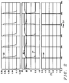
- the output swing of voltage V H is between V DDB and 0V as shown in Fig. 2 .
- Curve 20 shows the digital input signal ON.
- Curve 21 illustrates the drain voltage VH of the high voltage transistor HP1
- curve 22 shows the voltage Vc at the gate of the high voltage transistor HP1
- curve 23 shows the power dissipation of the high voltage transistor HP1 .
- Fig. 2 demonstrates that the circuit invented provides a reliable solution to drive the HV P-MOS power transistor HP1 with accurate gate-source control voltage Vc 22. Furthermore Fig. 2 shows the power dissipation 23 of the power transistor HP1 , the output voltage VH 22 responding to the digital input signal ON 20 , which is driven with a frequency of 50 kHz. On the other hand, a rapid switchable on/off is expected to avoid drawing static power.
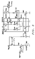
- Fig. 3 shows a complete circuit for driving HV-PMOS power transistor HP1.
- a new circuit structure is proposed in Fig. 3 .
- the highlighted control switches are added between the gate of HP1, V c , and the power supply V DDB .
- HP2 and HP3 are added to make switching on/off faster.
- the control circuit of HP2 and of HP3 are identical as of the HP1 , but they share the reference current I REF and HP3 is controlled by an inverted 5V digital signal inverted by inverter 30 .
- the resistors R3 and R4, each connecting a gate of HP3 or correspondently of HP4 with the supply voltage V DDB have the same resistance as resistor R2 connecting a gate of HP1 with the supply voltage V DDB , as shown already in Fig.1 .
- the operation of the circuit of Fig. 3 is described in two states, namely if the digital input signal ON is 5V and if the digital input signal ON is 0V.
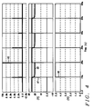
- Fig. 4 demonstrates that the circuit of Fig. 3 provides a significant improved solution to drive the HV P-MOS power transistor HP1 compared to the circuit shown in Fig. 1 .
- the digital input signal ON shown in Fig. 4 is driven with the same frequency of 50kHz as illustrated in the transient response charts of Fig. 2 .
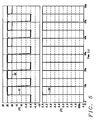
- Fig. 5 now, the frequency of the digital input signal ON 50 of the circuit shown in Fig. 3 has been increased from 50 kHz to 1 MHz.
- Fig. 5 demonstrates that the circuit shown in Fig. 3 can be operated with a frequency of 1 MHz.
- the power dissipation of transistor HP1 has been further improved since the dissipation is only produced by the turn-on and turn-off of the transistor HP1 , and is independent from the switching frequency as long as the switching period is larger than t ON +t OFF .
- Fig. 6 illustrates a flowchart of a method invented to achieve a fast switchable high voltage power transistor driver circuit.
- Step 60 of the method of Fig. 6 illustrates the provision of a circuit comprising a port for a high voltage supply voltage, a port for a low voltage supply voltage, an input stage comprising a high voltage power transistor, an output port, and a port for a digital input signal, and a control stage to achieve a constant gate-source voltage of the high voltage power transistor.
- Step 61 limiting the gate-source voltage of the high voltage power transistor using a voltage drop of a first reference current across a resistive load if the digital input signal is high.
- Step 62 describes pulling the gate of the high voltage power transistor to the level of the high voltage supply voltage if the digital input signal is low and step 63 teaches generating a second reference current, which is controlled by a reference voltage via a differential amplifier, wherein the second reference current is mirrored to the first reference current in order to establish an accurate gate source voltage of the high voltage.
Landscapes
- Engineering & Computer Science (AREA)
- Computer Hardware Design (AREA)
- Physics & Mathematics (AREA)
- Computing Systems (AREA)
- General Engineering & Computer Science (AREA)
- Mathematical Physics (AREA)
- Electronic Switches (AREA)
Abstract
Description
- This invention relates generally to transistor drivers and relates more specifically to a driver for a high voltage P-MOS power transistor having accurate control voltage and faster switching.
- For applications as e.g. automotive applications supply voltages up to 40 Volts and even higher are often required. High-Voltage CMOS devices are usually based on a 5V technology with an extended drain region to reach up to e.g. 40V drain-source breakdown capability. As the source side of the High-Voltage CMOS devices is the same as it is for 5-V CMOS devices, its bulk-source voltage, Vbs, as well as its gate-source voltage, Vgs, are limited to 5V. Static power dissipation of the high voltage (HV) transistors, achieving accurate control voltage of e.g. 5 Volts and high switching speed are key problems with high voltage CMOS devices, which should be overcome.
- It is a challenge for engineers designing driver circuits for high voltage applications, i.e. supply voltages in the order of magnitude of 40 V to overcome above problems.
- U. S. Patent (
US 6,507,226 to Swonger et al. ) discloses a circuit and method translating a logic level input signal to signals at high voltage levels to drive a power device, such as a power MOSFET, while minimizing the power consumption. The circuit for driving the power device includes a low side gate driver, and a high side gate driver adjacent thereto. The high side gate drive includes a high side gate driver logic input, a high side gate driver output, a latch connected between the high side gate driver logic input and the high side gate driver output, and a control circuit receiving an output of the latch and controlling signals from the high side gate driver logic input to the latch based upon the output of the latch. - U. S. Patent (
US 5,325,258 to Choi et al. ) discloses a circuit and method for driving a power transistor device. The circuit for driving a power transistor device has a driver having an input and an output, the output coupled to a control input of the power transistor device and the input coupled to a primary control voltage source for driving the power transistor device. A current sensing device is coupled to the power transistor device for providing a signal proportional to the current in the power transistor device. An amplifier is coupled to the current sensing device for providing a substantially linear control signal proportional to the current in the power transistor device, the linear control signal being provided to the input of the driver as a secondary drive signal for driving the power transistor device when a current level in the power transistor device greater than a threshold level is detected. A detector is provided for detecting when the current in the power transistor device is greater than the threshold level. The detector is coupled to the current sensing device and to a reference level source, and provides an overcurrent signal to the driver for switching the driver from being driven by the primary control voltage source to the secondary drive signal. The secondary drive signal drives the driver so as to reduce the current level in the power transistor device. The driven power transistor device is preferably a power MOSFET or IGBT. - U. S. Patent (
US 4,937,477 to Tsoi et al. ) proposes a high-voltage level translator circuit that is suitable for monolithic integration. The level translator circuit comprises serially connected current sources suitably ratioed so that the gating on of one current source causes a limited voltage rise across the other current source, which is ungated. The circuit is suitable for integration in a junction-isolated monolithic pseudo-complementary CMOS format. - A principal object of the present invention is to achieve an accurate control voltage for a high voltage power transistor.
- A further object of the invention is to establish an accurate control voltage independent of temperature and process variations.
- A further object of the invention is to minimize static power dissipation of a high voltage power transistor.
- Another object of the invention is to enhance switching speed of the high voltage power transistor.
- In accordance with the objects of this invention a method to provide a fast switchable high voltage power transistor driver circuit has been achieved. The method invented comprises, firstly, the following steps: (1) providing a circuit comprising a port for a high voltage supply voltage, a port for a low voltage supply voltage, an input stage comprising a high voltage power transistor, an output port, and a port for a digital input signal, and a control stage to achieve a constant gate-source voltage of the high voltage power transistor, and (2) limiting the gate-source voltage of the high voltage power transistor using a voltage drop of a first reference current across a resistive load if the digital input signal is high. Furthermore the method invented comprises the steps: (3) pulling the gate of the high voltage power transistor to the level of the high voltage supply voltage if the digital input signal is low, and (4) generating a second reference current, which is controlled by a reference voltage via a differential amplifier, wherein the second reference current is mirrored to the first reference current in order to establish an accurate gate source voltage of the high voltage.
- In accordance with the objects of this invention a fast switchable high voltage power transistor driver circuit has been achieved. The driver circuit invented comprises, firstly an input stage comprising: a port for a high voltage supply voltage, a port for a digital input signal, and a high voltage power transistor connected between said high voltage supply port and an output port of the circuit. Furthermore the input stage comprises a resistive load connected between a gate of the high voltage power transistor and the high voltage supply port, a high voltage transistor being connected between the gate of the high voltage power transistor and a low voltage transistor, and said low voltage transistor connected between the high voltage transistor and ground wherein the gate of the low voltage transistor is connected to a gate of a fourth transistor of a control stage. Furthermore the driver circuit comprises a control stage comprising: a port of a low voltage supply voltage, a differential amplifier having inputs and an output, wherein a first input is connected to a port of a reference voltage, a second input is a voltage of a first terminal of a first means of resistance, and the output is connected to a gate of a first transistor, and said means of resistance, wherein the first terminal is connected to the first transistor and a second terminal is connected to ground. Furthermore the control stage comprises said first transistor connected between said means of resistance and a second transistor, said second transistor connected between said first transistor and the port for low supply voltage, wherein the second transistor is forming a first current mirror with a third transistor, said third transistor connected between the port for the low voltage supply voltage and the fourth transistor, and said fourth transistor connected between the third transistor and ground, wherein the fourth transistor is forming a second current mirror with said low voltage transistor of the input stage.
- In the accompanying drawings forming a material part of this description, there is shown:
-
Fig. 1 shows a schematic of the principles of the invented circuit driving a HV P-MOS power transistor. -
Fig. 2 depicts the transient response of the circuit ofFig. 1 with VDDB=25V and Cload=1nF. -
Fig. 3 shows a complete circuit for driving an HV-PMOS power transistor. -
Fig. 4 shows the transient responses of the circuit ofFig. 3 with VDDB=25V, and Cload=1nF, and operating frequency of 50 kHz. -
Fig. 5 shows the transient response of the circuit shown inFig. 3 with VDDB=25V, and operating frequency of 1 MHz. -
Fig. 6 illustrates a flowchart of a method invented to achieve a fast switchable high voltage power transistor driver circuit. - Methods and circuits to achieve an accurate control voltage of a high voltage power transistor combined with a rapid switching-on and switching-off operation of a high voltage power transistor are disclosed.
-
Fig. 1 shows principles of a preferred embodiment of the present invention, i.e. a schematic of a circuit driving a HV P-MOS power transistor (HP1). It should be noted that the invention could be applied to other power transistors with drain-source voltage capability higher than 5V and gate-source voltage limited to 5V. - The circuit shown in
Fig. 1 to drive the HV P-MOS power transistor, HP1, is supplied directly by power supply, VDDB, with an input comprised of HV N-MOS transistor, HN1, directly controlled by 5V digital signal. In the preferred embodiment the power supply voltage VDDB can vary between 5.5 V and 40 V. Other ranges of voltages are possible as well, depending on e.g. the type of high voltage power transistor used. The HV power transistors deployed have an extended drain region to reach up to 40 V drain source breakdown capability. As the source side of the High-Voltage CMOS devices is the same as it is for 5-V CMOS devices, its bulk-source voltage, Vbs, as well as its gate-source voltage, Vgs, are limited to 5V. - The input stage has a resistive load of R2 (e.g. 50kΩ) that pulls the gate of HP1 to VDDB, if the digital input signal ON is low ( ON = 0V). The resistive load, R2, together with the controlled input stage reference-current IREF serves as gate source limitation of IREF* R2 when the digital input signal ON is high (ON = 5V).
- However the gate-source limitation of IREF* R2 varies with current and resistor temperature / process changes, which needs to be cancelled. The circuit that cancels the variation uses an
amplifier 1 to mirror a fixed voltage, VREF, across a resistor R1, which is matched to that resistive load of R2 according to the equation R1 = R2/K., wherein the factor K corresponds to the equation K = VDDL/VREF or, according to the values of voltages used in the preferred embodiment illustrated inFig. 1 , K = 5V/1.65V = 3.03. It should be understood that these values are examples only and that other values of K and voltages could be applied as well. These values depend also on the types of high voltage transistors used. - The accurate matching of 5V MOS devices allows an accurate current ratio to be generated. Using the current ratios CM1 = P3/P2 = 1 of the 5V P-MOS mirror, comprising P-MOS transistors 2 and 3 (P2 is the gate-drain connected P-MOS transistor) and CM2 = N1/N2 = 1 of the 5V N-MOS mirror, comprising
transistors N1 5 andN2 4, which is a gate-drain connected N-MOS transistor, an output current is generated, resulting in an accurate voltage limitation of IREF* R2 = (VREF/ R1)* R2=K* VREF= 5V. More generally formulated K = VDDL/VREF. - It should be noted that alternatively other current mirror ratios than 1:1 can be used as well, i.e. CM1 and CM2 result in an accurate voltage limitation of IREF*R2 = (VREF/ R1)*CM1*CM2*R2 = CM1*CM2*(R2/R1)*VREF = VDDL= 5V, and K = VDDL/VREF = CM1*CM2*(R2/R1).
- The HV-NMOS device HN1, also isolates the 5V-NMOS device N1, from the high voltage domain.
- The output swing of the voltage Vc at the gate of the HV P-MOS transistor HP1 is between VDDB and VDDB - 5V, and the output swing of voltage VH is between VDDB and 0V as shown in
Fig. 2 . -
Fig. 2 illustrates the transient response of the circuit invented shown inFig. 1 with voltage VDDB = 25V and CLOAD = 1 nF. The load capacitance CLOAD is limited by the slew rate from the output swing of voltage VH of the HV P-MOS transistor HP1 as
for given requirement. The switching frequency is however only limited by the slew rate from the input swing of voltage Vc of the HV P-MOS transistor HP1 as τ1 = R2*CGS_HP1 inFig. 1 . -
Curve 20 shows the digital input signal ON.Curve 21 illustrates the drain voltage VH of the high voltage transistor HP1,curve 22 shows the voltage Vc at the gate of the high voltage transistor HP1, andcurve 23 shows the power dissipation of the high voltage transistor HP1.Curve 23 shows the power dissipation in watt (=|lCTRL*(5V-Vc(t,τ1)|) to turn-on and turn-off of the HP1 inFig. 1 . -
Fig. 2 demonstrates that the circuit invented provides a reliable solution to drive the HV P-MOS power transistor HP1 with accurate gate-sourcecontrol voltage Vc 22. FurthermoreFig. 2 shows thepower dissipation 23 of the power transistor HP1, theoutput voltage VH 22 responding to the digital input signal ON 20, which is driven with a frequency of 50 kHz. On the other hand, a rapid switchable on/off is expected to avoid drawing static power. - Because of the parasitic capacitance across the gate-source of the HP1 due to its large sizing (WxL=16'000x2.7), its
control voltage Vc 22 changes with a time constant τ1 = R2* CGS_HP1, from VDDB to VDDB -5V, as well as from VDDB -5V to VDDB., wherein CGS is the gate-source capacitance of transistor HP1 This limits the switching speed and makes larger static power loss during on/off phases. -
Fig. 3 shows a complete circuit for driving HV-PMOS power transistor HP1. In order to simultaneously have a rapid switching operation, a new circuit structure is proposed inFig. 3 . The highlighted control switches are added between the gate of HP1, Vc, and the power supply VDDB. To make switching on/off faster, two smaller sizing HV P-MOS devices, HP2 and HP3 (e.g. having a size of =100x2.7), are added. The control circuit of HP2 and of HP3 are identical as of the HP1, but they share the reference current IREF and HP3 is controlled by an inverted 5V digital signal inverted byinverter 30. The resistors R3 and R4, each connecting a gate of HP3 or correspondently of HP4 with the supply voltage VDDB, have the same resistance as resistor R2 connecting a gate of HP1 with the supply voltage VDDB, as shown already inFig.1 . In the following the operation of the circuit ofFig. 3 is described in two states, namely if the digital input signal ON is 5V and if the digital input signal ON is 0V. - When signal ON is 5V, the gate voltage of HP2 VG_HP2, charges from VDDB to VDDB- 5V. The source voltage of HP2 VS_HP2, which is above a diode threshold voltage higher than its gate voltage, charges from VDDB to VDDB - VG_HP2 + |VGS_HP2| ∼ VDDB - 5V + 0.7V = VDDB - 4.3V having a time constant of τ 2 = R3* CGS_HP2. Therefore the control voltage, Vc , settles now from VDDB to VDDB - 4.3V witch τ 2 = R3*CGS_HP2, and then settles from VDDB - 4.3V to VDDB - 5V with time constants τ1 = R2*CGS_HP1. Since the parasitic capacitance at the gate of HP2 is much smaller than that at the gate of HP1 resulting time constant τ 2 << τ 1; thus a faster switching-on is achieved.
- When signal ON is 0V and the inverted digital signal at the output of
inverter 30 is 5V), the gate voltage of transistor HP3, VG_HP3, charges from VDDB to VDDB-5V and closes its drain-source voltage with an on-resistance of RDSON_HP3 aborve 200 Ω. Therefore the control voltage Vc discharges now from VDDB - 5V to VDDB with τ3 = RDSON_HP3 * CGS_HP1 rather than with τ1 = R2* CGS_HP1; thus a faster switching-off is achieved. -
Fig. 4 shows the transient responses of the circuit ofFig. 3 with supply voltage VDDB=25V, and Cload=1nF.Fig. 4 demonstrates that the circuit ofFig. 3 provides a significant improved solution to drive the HV P-MOS power transistor HP1 compared to the circuit shown inFig. 1 . The digital input signal ON, shown inFig. 4 is driven with the same frequency of 50kHz as illustrated in the transient response charts ofFig. 2 . - Comparing the response to the digital input signal ON 40 of the
power dissipation 43 of the power transistor HP1, of thecontrol voltage VC 42, and of theoutput voltage VH 42 shown inFig. 4 with the correspondent curves ofFig. 2 it is clearly demonstrated that the circuit ofFig. 3 has less power dissipation and better time constants for Vc and VH as outlined above. - Turning to
Fig. 5 now, the frequency of the digital input signal ON 50 of the circuit shown inFig. 3 has been increased from 50 kHz to 1 MHz.Fig. 5 demonstrates that the circuit shown inFig. 3 can be operated with a frequency of 1 MHz. Moreover the power dissipation of transistor HP1 has been further improved since the dissipation is only produced by the turn-on and turn-off of the transistor HP1, and is independent from the switching frequency as long as the switching period is larger than tON+tOFF. -
Fig. 6 illustrates a flowchart of a method invented to achieve a fast switchable high voltage power transistor driver circuit. -
Step 60 of the method ofFig. 6 illustrates the provision of a circuit comprising a port for a high voltage supply voltage, a port for a low voltage supply voltage, an input stage comprising a high voltage power transistor, an output port, and a port for a digital input signal, and a control stage to achieve a constant gate-source voltage of the high voltage power transistor.Step 61 limiting the gate-source voltage of the high voltage power transistor using a voltage drop of a first reference current across a resistive load if the digital input signal is high.Step 62 describes pulling the gate of the high voltage power transistor to the level of the high voltage supply voltage if the digital input signal is low andstep 63 teaches generating a second reference current, which is controlled by a reference voltage via a differential amplifier, wherein the second reference current is mirrored to the first reference current in order to establish an accurate gate source voltage of the high voltage. - While the invention has been particularly shown and described with reference to the preferred embodiments thereof, it will be understood by those skilled in the art that various changes in form and details may be made without departing from the spirit and scope of the invention.
Claims (26)
- A method to achieve a fast switchable high voltage power transistor driver circuit, comprising the following steps:(1) providing a circuit comprising a port for a high voltage supply voltage, a port for a low voltage supply voltage, an input stage comprising a high voltage power transistor, an output port, and a port for a digital input signal, and a control stage to achieve a constant gate-source voltage of the high voltage power transistor;(2) limiting the gate-source voltage of the high voltage power transistor using a voltage drop of a first reference current across a resistive load if the digital input signal is high;(3) pulling the gate of the high voltage power transistor to the level of the high voltage supply voltage if the digital input signal is low; and(4) generating a second reference current, which is controlled by a reference voltage via a differential amplifier, wherein the second reference current is mirrored to the first reference current in order to establish an accurate gate source voltage of the high voltage.
- The method of claim 1 wherein the high voltage supply voltage can vary between a voltage in the order of magnitude of about 5.5 Volts and a voltage in the order of magnitude of about 40Volts and wherein the low voltage supply voltage is in the order of magnitude of about 5Volts.
- The method of claim 1 wherein the high voltage power transistor can be any power transistor with drain-source voltage capability higher than 5V and gate-source voltage limited to 5V, such as a a high voltage P-MOS transistor having an extended drain region.
- The method of claim 1 wherein the port for the digital input signal is a gate of a high voltage N-MOS transistor, e.g. having an extended drain region for isolating a low voltage transistor, used for mirroring the first reference current to the second reference current, from a high voltage domain.
- The method of claim 1 wherein the second reference current is generated by mirroring a fixed reference voltage by said amplifier a cross a resistive means, which is matched to the resistive load.
- The method of claim 5 wherein the second reference is mirrored to the first reference current via two current mirrors wherein both current mirrors comprise low voltage transistors.
- The method of claim 1 wherein generation of the second reference current and the mirroring to the first reference current is performed in a low voltage region.
- The method of claim 1 wherein the swing of the output port is from the high voltage supply voltage to 0 Volts.
- The method of claim 1 wherein the swing of the gate of the high voltage power transistor is from the high voltage supply voltage - allowable gate source voltage.
- The method of claim 1 wherein time constants for switching on and off the power transistor are reduced by adding two high voltage transistors of the same type as the high voltage power transistor to the circuit in parallel to the input stage in order to increase the operation frequency of the circuit, wherein each of both additional transistors is smaller than the high voltage power transistor.
- The method of claim 10 wherein both control circuits of each of said additional high voltage transistors are identical to the control circuit of the high voltage power transistor but they share one reference current and a second transistor of these two additional high voltage transistors is controlled by an inverted signal.
- The method of claim 1 wherein said second reference current is mirrored to the first reference current with a ratio of 1:1.
- A fast switchable high voltage power transistor driver circuit comprising:an input stage comprising:a port for a high voltage supply voltage;a port for a digital input signal;a high voltage power transistor connected between said high voltage supply port and an output port of the circuit;a resistive load connected between a gate of the high voltage power transistor and the high voltage supply port;a high voltage transistor being connected between the gate of the high voltage power transistor and a low voltage transistor; andsaid low voltage transistor connected between the high voltage transistor andground wherein the gate of the low voltage transistor is connected to a gate ofa fourth transistor of a control stage; anda control stage comprising:a port of a low voltage supply voltage;a differential amplifier having inputs and an output, wherein a first input is connected to a port of a reference voltage, a second input is a voltage of a first terminal of a first means of resistance, and the output is connected to a gate of a first transistor;said means of resistance, wherein the first terminal is connected to the first transistor and a second terminal is connected to ground;said first transistor connected between said means of resistance and a second transistor;said second transistor connected between said first transistor and the port for low supply voltage, wherein the second transistor is forming a first current mirror with a third transistor;said third transistor connected between the port for the low voltage supply voltage and the fourth transistor; andsaid fourth transistor connected between the third transistor and ground,wherein the fourth transistor is forming a second current mirror with said low voltage transistor of the input stage.
- The driver circuit of claim 13 wherein the high voltage supply voltage can vary between a voltage in the order of magnitude of about 5.5 Volts and a voltage in the order of magnitude of about 40Volts and wherein the low voltage supply voltage is in the order of magnitude of about 5Volts.
- The driver circuit of claim 13 wherein the high voltage power transistor is a high voltage P-MOS transistor, e.g. a high voltage P-MOS transistor power having an extended drain region.
- The driver circuit of claim 13 wherein the high voltage transistor is a high voltage NMOS transistor, e.g. a high voltage N-MOS transistor has an extended drain region.
- The driver circuit of claim 16 wherein the port for the digital input signal is a gate of the high voltage N-MOS transistor
- The driver circuit of claim 13 wherein the high voltage N-MOS transistor isolates a low voltage transistor, used for mirroring the first reference current to the second reference current, from a high voltage domain.
- The driver circuit of claim 13 wherein said first current mirror has a scale of 1: 1 and/or wherein said second current mirror has a scale of 1: 1.
- The driver circuit of claim 13 wherein said resistive means has a resistance R according to the equation R = resistance of the resistive load divided by a factor K, wherein K = low supply voltage divided by said reference voltage.
- The driver circuit of claim 13 wherein the swing of the output port is from the high voltage supply voltage to 0 Volts and wherein the swing of the gate of the high voltage power transistor is from the high voltage supply voltage - allowable gate source voltage.
- The driver circuit of claim 13 wherein time constants for switching on and off the power transistor are reduced by adding two high voltage transistors of the same type as the high voltage power transistor to the circuit in paralle3l to the input stage in order to increase the operation frequency of the circuit, wherein each of both additional transistors is smaller than the high voltage power transistor.
- The driver circuit of claim 22 wherein both control circuits of each of these additional high voltage transistors are identical to the control circuit of the high voltage power transistor but they share one reference current and a second transistor of these two additional high voltage transistors is controlled by an inverted signal.
- The driver circuit of claim 22 wherein a circuitry to connect these additional transistors comprises:a first of said two additional high voltage transistors being connected between the high voltage supply voltage and the gate of the high voltage power transistor, wherein its gate is connected via a second resistive means to the high supply voltage and to a drain of a third additional high voltage transistor;a second of said two additional high voltage transistors being connected between the gate of the high voltage power transistor and ground, wherein its gate is connected via a third resistive means to the high supply voltage and to a drain of a fourth additional high voltage transistor;said second resistive means;said third resistive means;said third additional high voltage transistor having its source connected to a source of the fourth additional high voltage transistor and to a drain of a fifth low voltage transistor and its gate is connected to an output of an inverter;said fourth additional high voltage transistor having its gate connected to the port for a digital input signal;said inverter having its input connected to the port for a digital input signal; andsaid fifth low voltage transistor having its source connected to ground and its gate is connected to the gates of said second current mirror.
- The driver circuit of claim 24 wherein said second and said third resistive means have a same resistance as said resistive load, and.
wherein each of said first and second additional high voltage transistors are P-MOS transistors and each of both transistors are smaller than the high voltage power transistor. - The driver circuit of claim 24 wherein each of said third and fourth additional high voltage transistors are NMOS transistors and wherein said fifth low voltage transistor is a NMOS transistor.
Priority Applications (1)
| Application Number | Priority Date | Filing Date | Title |
|---|---|---|---|
| EP11368019.3A EP2498404B1 (en) | 2011-03-07 | 2011-05-12 | A rapid switchable HV P-MOS power transistor driver with constant gate-source control voltage |
Applications Claiming Priority (2)
| Application Number | Priority Date | Filing Date | Title |
|---|---|---|---|
| EP11368005 | 2011-03-07 | ||
| EP11368019.3A EP2498404B1 (en) | 2011-03-07 | 2011-05-12 | A rapid switchable HV P-MOS power transistor driver with constant gate-source control voltage |
Publications (2)
| Publication Number | Publication Date |
|---|---|
| EP2498404A1 true EP2498404A1 (en) | 2012-09-12 |
| EP2498404B1 EP2498404B1 (en) | 2015-09-09 |
Family
ID=44118483
Family Applications (1)
| Application Number | Title | Priority Date | Filing Date |
|---|---|---|---|
| EP11368019.3A Active EP2498404B1 (en) | 2011-03-07 | 2011-05-12 | A rapid switchable HV P-MOS power transistor driver with constant gate-source control voltage |
Country Status (2)
| Country | Link |
|---|---|
| US (1) | US8664997B2 (en) |
| EP (1) | EP2498404B1 (en) |
Cited By (2)
| Publication number | Priority date | Publication date | Assignee | Title |
|---|---|---|---|---|
| EP3723287A1 (en) * | 2019-04-11 | 2020-10-14 | Koninklijke Philips N.V. | Ultrasound transducer driver circuit |
| EP3928403A4 (en) * | 2019-02-22 | 2022-04-20 | Texas Instruments Incorporated | DISABLE CIRCUIT FOR PROTECTIVE SWITCH |
Families Citing this family (8)
| Publication number | Priority date | Publication date | Assignee | Title |
|---|---|---|---|---|
| US8497725B2 (en) * | 2011-08-26 | 2013-07-30 | Texas Instruments Incorporated | Active pull-up/pull-down circuit |
| CN105897246B (en) * | 2014-12-26 | 2020-10-02 | 恩智浦美国有限公司 | Voltage level shifter for high voltage applications |
| US10071652B2 (en) | 2016-05-11 | 2018-09-11 | Ford Global Technologies, Llc | Dual mode IGBT gate drive to reduce switching loss |
| DE102017208187B4 (en) * | 2017-05-16 | 2025-10-30 | Continental Automotive Technologies GmbH | Electronic module, motor vehicle, and method for limiting an input current during a switch-on process of the module |
| US10181849B1 (en) | 2017-11-29 | 2019-01-15 | Nxp B.V. | Transistor control terminal control circuit |
| CN108512536B (en) * | 2018-07-10 | 2023-11-28 | 上海艾为电子技术股份有限公司 | Analog switch with constant on-resistance |
| US10819351B1 (en) * | 2019-05-28 | 2020-10-27 | Texas Instruments Incorporated | Gate driver circuit with a closed loop overdrive generator |
| JP7543653B2 (en) * | 2020-02-05 | 2024-09-03 | 株式会社デンソー | MOSFET driver circuit |
Citations (5)
| Publication number | Priority date | Publication date | Assignee | Title |
|---|---|---|---|---|
| US4937477A (en) | 1988-01-19 | 1990-06-26 | Supertex, Inc. | Integrated mos high-voltage level-translation circuit, structure and method |
| US5325258A (en) | 1992-08-26 | 1994-06-28 | International Rectifier Corporation | Power transistor driver circuit with current sensing and current overprotection and method for protecting power transistor from overcurrent |
| US6078204A (en) * | 1996-12-19 | 2000-06-20 | Texas Instruments Incorporated | High current drain-to-gate clamp/gate-to-source clamp for external power MOS transistors |
| US6507226B2 (en) | 2000-07-31 | 2003-01-14 | Intersil Americas Inc. | Power device driving circuit and associated methods |
| US20050258876A1 (en) * | 2004-05-21 | 2005-11-24 | Dake Luthuli E | System for producing high-voltage, low-power driver circuitry |
Family Cites Families (22)
| Publication number | Priority date | Publication date | Assignee | Title |
|---|---|---|---|---|
| DE4329867C1 (en) * | 1993-09-03 | 1994-09-15 | Siemens Ag | Current mirror |
| KR0134661B1 (en) * | 1995-04-24 | 1998-04-25 | 김광호 | Potential current converter |
| DE19814675A1 (en) * | 1997-04-03 | 1998-10-08 | Fuji Electric Co Ltd | Output circuit for power IC with high breakdown voltage |
| JP3031313B2 (en) * | 1997-09-11 | 2000-04-10 | 日本電気株式会社 | Semiconductor circuit |
| FR2800532B1 (en) * | 1999-10-28 | 2002-01-04 | Pixtech Sa | VERY HIGH VOLTAGE SWITCH |
| CH697322B1 (en) * | 2000-06-13 | 2008-08-15 | Em Microelectronic Marin Sa | A method of generating a substantially Independent current temperature and device for carrying out this method. |
| KR100441248B1 (en) * | 2001-02-22 | 2004-07-21 | 삼성전자주식회사 | Current generating circuit insensivitve to resistance variation |
| US6977523B2 (en) * | 2002-09-27 | 2005-12-20 | Oki Electric Industry Co., Ltd. | Voltage level shifting circuit |
| US7235451B2 (en) * | 2003-03-03 | 2007-06-26 | Texas Instruments Incorporated | Drain extended MOS devices with self-aligned floating region and fabrication methods therefor |
| EP1582418A1 (en) * | 2004-03-30 | 2005-10-05 | Dialog Semiconductor GmbH | Squib driver for airbag application |
| US7180140B1 (en) * | 2004-04-16 | 2007-02-20 | National Semiconductor Corporation | PMOS device with drain junction breakdown point located for reduced drain breakdown voltage walk-in and method for designing and manufacturing such device |
| DE102004019345B4 (en) * | 2004-04-21 | 2007-02-08 | Austriamicrosystems Ag | Output stage system |
| KR100629520B1 (en) * | 2005-02-22 | 2006-09-28 | 삼성전자주식회사 | Ultra Low Power Voltage Conversion Circuit |
| DE102005039138B4 (en) * | 2005-08-18 | 2012-07-12 | Infineon Technologies Ag | By means of a resistor programmable and a reference current source having circuit |
| US7388387B2 (en) * | 2006-01-11 | 2008-06-17 | Stratosphere Solutions, Inc. | Method and apparatus for measurement of electrical resistance |
| JP2009088766A (en) * | 2007-09-28 | 2009-04-23 | Toshiba Corp | Output buffer circuit |
| US7560972B1 (en) * | 2008-01-29 | 2009-07-14 | Texas Instruments Incorporated | Methods and apparatus to reduce propagation delay of circuits |
| US7679420B1 (en) * | 2008-08-28 | 2010-03-16 | Micrel, Incorporated | Slew rate controlled level shifter with reduced quiescent current |
| JP2010109838A (en) * | 2008-10-31 | 2010-05-13 | Nec Electronics Corp | Level shift circuit |
| US8410839B2 (en) * | 2009-02-20 | 2013-04-02 | Conexant Systems, Inc. | Systems and methods for driving high power states using lower voltage processes |
| US8125808B2 (en) * | 2009-09-28 | 2012-02-28 | Harris Corporation | Three-phase low-loss rectifier |
| KR101431880B1 (en) * | 2011-08-12 | 2014-08-27 | 삼성전기주식회사 | Output driving circuit and transistor output circuit |
-
2011
- 2011-03-11 US US12/932,994 patent/US8664997B2/en active Active
- 2011-05-12 EP EP11368019.3A patent/EP2498404B1/en active Active
Patent Citations (5)
| Publication number | Priority date | Publication date | Assignee | Title |
|---|---|---|---|---|
| US4937477A (en) | 1988-01-19 | 1990-06-26 | Supertex, Inc. | Integrated mos high-voltage level-translation circuit, structure and method |
| US5325258A (en) | 1992-08-26 | 1994-06-28 | International Rectifier Corporation | Power transistor driver circuit with current sensing and current overprotection and method for protecting power transistor from overcurrent |
| US6078204A (en) * | 1996-12-19 | 2000-06-20 | Texas Instruments Incorporated | High current drain-to-gate clamp/gate-to-source clamp for external power MOS transistors |
| US6507226B2 (en) | 2000-07-31 | 2003-01-14 | Intersil Americas Inc. | Power device driving circuit and associated methods |
| US20050258876A1 (en) * | 2004-05-21 | 2005-11-24 | Dake Luthuli E | System for producing high-voltage, low-power driver circuitry |
Non-Patent Citations (1)
| Title |
|---|
| KHORASANI M ET AL: "Low-power static and dynamic high-voltage CMOS level-shifter circuits", CIRCUITS AND SYSTEMS, 2008. ISCAS 2008. IEEE INTERNATIONAL SYMPOSIUM ON, IEEE, PISCATAWAY, NJ, USA, 18 May 2008 (2008-05-18), pages 1946 - 1949, XP031392380, ISBN: 978-1-4244-1683-7 * |
Cited By (3)
| Publication number | Priority date | Publication date | Assignee | Title |
|---|---|---|---|---|
| EP3928403A4 (en) * | 2019-02-22 | 2022-04-20 | Texas Instruments Incorporated | DISABLE CIRCUIT FOR PROTECTIVE SWITCH |
| EP3723287A1 (en) * | 2019-04-11 | 2020-10-14 | Koninklijke Philips N.V. | Ultrasound transducer driver circuit |
| WO2020208048A1 (en) | 2019-04-11 | 2020-10-15 | Koninklijke Philips N.V. | Ultrasound transducer driver circuit |
Also Published As
| Publication number | Publication date |
|---|---|
| US8664997B2 (en) | 2014-03-04 |
| US20120229173A1 (en) | 2012-09-13 |
| EP2498404B1 (en) | 2015-09-09 |
Similar Documents
| Publication | Publication Date | Title |
|---|---|---|
| EP2498404B1 (en) | A rapid switchable HV P-MOS power transistor driver with constant gate-source control voltage | |
| JP3915815B2 (en) | Level shift circuit and power supply device | |
| CN102684292B (en) | Power supply switching circuit | |
| US10211826B2 (en) | Electronic switch, and corresponding device and method | |
| US8044950B2 (en) | Driver circuit usable for display panel | |
| KR100402667B1 (en) | Level - shifting pass gate | |
| CN111313878B (en) | An analog switch circuit | |
| JPWO2014196136A1 (en) | Gate driver and power module including the same | |
| US6828846B2 (en) | Analog switch circuit | |
| JP2023063081A (en) | Switching circuit, dc/dc converter, and control circuit for the same | |
| CN101672867A (en) | Overcurrent detection circuit | |
| US7724069B1 (en) | Analog switch for operation outside power rails with low supply current | |
| US6437622B1 (en) | Temperature compensated slew rate control circuit | |
| KR980012402A (en) | Analog switch circuit | |
| JPH0626309B2 (en) | Output circuit | |
| JPH0563962B2 (en) | ||
| JP2012147084A (en) | Output circuit | |
| US20210356981A1 (en) | Startup circuit and bandgap reference circuit | |
| CN111211763B (en) | High potential side driving circuit | |
| US20150236692A1 (en) | Driving signal generating circuit and power semiconductor device driving apparatus including the same | |
| JP3863474B2 (en) | Drive circuit and semiconductor device | |
| JP3426337B2 (en) | Zero bias current low side driver control circuit | |
| US7733154B2 (en) | Semiconductor device | |
| US10819351B1 (en) | Gate driver circuit with a closed loop overdrive generator | |
| JP2003338740A (en) | High voltage switching circuit |
Legal Events
| Date | Code | Title | Description |
|---|---|---|---|
| PUAI | Public reference made under article 153(3) epc to a published international application that has entered the european phase |
Free format text: ORIGINAL CODE: 0009012 |
|
| AK | Designated contracting states |
Kind code of ref document: A1 Designated state(s): AL AT BE BG CH CY CZ DE DK EE ES FI FR GB GR HR HU IE IS IT LI LT LU LV MC MK MT NL NO PL PT RO RS SE SI SK SM TR |
|
| AX | Request for extension of the european patent |
Extension state: BA ME |
|
| 17P | Request for examination filed |
Effective date: 20130311 |
|
| GRAP | Despatch of communication of intention to grant a patent |
Free format text: ORIGINAL CODE: EPIDOSNIGR1 |
|
| INTG | Intention to grant announced |
Effective date: 20150319 |
|
| GRAS | Grant fee paid |
Free format text: ORIGINAL CODE: EPIDOSNIGR3 |
|
| GRAA | (expected) grant |
Free format text: ORIGINAL CODE: 0009210 |
|
| AK | Designated contracting states |
Kind code of ref document: B1 Designated state(s): AL AT BE BG CH CY CZ DE DK EE ES FI FR GB GR HR HU IE IS IT LI LT LU LV MC MK MT NL NO PL PT RO RS SE SI SK SM TR |
|
| REG | Reference to a national code |
Ref country code: GB Ref legal event code: FG4D |
|
| REG | Reference to a national code |
Ref country code: AT Ref legal event code: REF Ref document number: 748860 Country of ref document: AT Kind code of ref document: T Effective date: 20150915 Ref country code: CH Ref legal event code: EP |
|
| REG | Reference to a national code |
Ref country code: IE Ref legal event code: FG4D |
|
| REG | Reference to a national code |
Ref country code: DE Ref legal event code: R096 Ref document number: 602011019561 Country of ref document: DE |
|
| REG | Reference to a national code |
Ref country code: NL Ref legal event code: MP Effective date: 20150909 |
|
| PG25 | Lapsed in a contracting state [announced via postgrant information from national office to epo] |
Ref country code: NO Free format text: LAPSE BECAUSE OF FAILURE TO SUBMIT A TRANSLATION OF THE DESCRIPTION OR TO PAY THE FEE WITHIN THE PRESCRIBED TIME-LIMIT Effective date: 20151209 Ref country code: LT Free format text: LAPSE BECAUSE OF FAILURE TO SUBMIT A TRANSLATION OF THE DESCRIPTION OR TO PAY THE FEE WITHIN THE PRESCRIBED TIME-LIMIT Effective date: 20150909 Ref country code: FI Free format text: LAPSE BECAUSE OF FAILURE TO SUBMIT A TRANSLATION OF THE DESCRIPTION OR TO PAY THE FEE WITHIN THE PRESCRIBED TIME-LIMIT Effective date: 20150909 Ref country code: GR Free format text: LAPSE BECAUSE OF FAILURE TO SUBMIT A TRANSLATION OF THE DESCRIPTION OR TO PAY THE FEE WITHIN THE PRESCRIBED TIME-LIMIT Effective date: 20151210 Ref country code: LV Free format text: LAPSE BECAUSE OF FAILURE TO SUBMIT A TRANSLATION OF THE DESCRIPTION OR TO PAY THE FEE WITHIN THE PRESCRIBED TIME-LIMIT Effective date: 20150909 |
|
| REG | Reference to a national code |
Ref country code: LT Ref legal event code: MG4D |
|
| REG | Reference to a national code |
Ref country code: AT Ref legal event code: MK05 Ref document number: 748860 Country of ref document: AT Kind code of ref document: T Effective date: 20150909 |
|
| PG25 | Lapsed in a contracting state [announced via postgrant information from national office to epo] |
Ref country code: RS Free format text: LAPSE BECAUSE OF FAILURE TO SUBMIT A TRANSLATION OF THE DESCRIPTION OR TO PAY THE FEE WITHIN THE PRESCRIBED TIME-LIMIT Effective date: 20150909 Ref country code: SE Free format text: LAPSE BECAUSE OF FAILURE TO SUBMIT A TRANSLATION OF THE DESCRIPTION OR TO PAY THE FEE WITHIN THE PRESCRIBED TIME-LIMIT Effective date: 20150909 Ref country code: ES Free format text: LAPSE BECAUSE OF FAILURE TO SUBMIT A TRANSLATION OF THE DESCRIPTION OR TO PAY THE FEE WITHIN THE PRESCRIBED TIME-LIMIT Effective date: 20150909 Ref country code: HR Free format text: LAPSE BECAUSE OF FAILURE TO SUBMIT A TRANSLATION OF THE DESCRIPTION OR TO PAY THE FEE WITHIN THE PRESCRIBED TIME-LIMIT Effective date: 20150909 |
|
| PG25 | Lapsed in a contracting state [announced via postgrant information from national office to epo] |
Ref country code: NL Free format text: LAPSE BECAUSE OF FAILURE TO SUBMIT A TRANSLATION OF THE DESCRIPTION OR TO PAY THE FEE WITHIN THE PRESCRIBED TIME-LIMIT Effective date: 20150909 |
|
| PG25 | Lapsed in a contracting state [announced via postgrant information from national office to epo] |
Ref country code: EE Free format text: LAPSE BECAUSE OF FAILURE TO SUBMIT A TRANSLATION OF THE DESCRIPTION OR TO PAY THE FEE WITHIN THE PRESCRIBED TIME-LIMIT Effective date: 20150909 Ref country code: IS Free format text: LAPSE BECAUSE OF FAILURE TO SUBMIT A TRANSLATION OF THE DESCRIPTION OR TO PAY THE FEE WITHIN THE PRESCRIBED TIME-LIMIT Effective date: 20160109 Ref country code: IT Free format text: LAPSE BECAUSE OF FAILURE TO SUBMIT A TRANSLATION OF THE DESCRIPTION OR TO PAY THE FEE WITHIN THE PRESCRIBED TIME-LIMIT Effective date: 20150909 Ref country code: SK Free format text: LAPSE BECAUSE OF FAILURE TO SUBMIT A TRANSLATION OF THE DESCRIPTION OR TO PAY THE FEE WITHIN THE PRESCRIBED TIME-LIMIT Effective date: 20150909 Ref country code: CZ Free format text: LAPSE BECAUSE OF FAILURE TO SUBMIT A TRANSLATION OF THE DESCRIPTION OR TO PAY THE FEE WITHIN THE PRESCRIBED TIME-LIMIT Effective date: 20150909 |
|
| PG25 | Lapsed in a contracting state [announced via postgrant information from national office to epo] |
Ref country code: PT Free format text: LAPSE BECAUSE OF FAILURE TO SUBMIT A TRANSLATION OF THE DESCRIPTION OR TO PAY THE FEE WITHIN THE PRESCRIBED TIME-LIMIT Effective date: 20160111 Ref country code: RO Free format text: LAPSE BECAUSE OF FAILURE TO SUBMIT A TRANSLATION OF THE DESCRIPTION OR TO PAY THE FEE WITHIN THE PRESCRIBED TIME-LIMIT Effective date: 20150909 Ref country code: AT Free format text: LAPSE BECAUSE OF FAILURE TO SUBMIT A TRANSLATION OF THE DESCRIPTION OR TO PAY THE FEE WITHIN THE PRESCRIBED TIME-LIMIT Effective date: 20150909 Ref country code: PL Free format text: LAPSE BECAUSE OF FAILURE TO SUBMIT A TRANSLATION OF THE DESCRIPTION OR TO PAY THE FEE WITHIN THE PRESCRIBED TIME-LIMIT Effective date: 20150909 |
|
| REG | Reference to a national code |
Ref country code: DE Ref legal event code: R097 Ref document number: 602011019561 Country of ref document: DE |
|
| PLBE | No opposition filed within time limit |
Free format text: ORIGINAL CODE: 0009261 |
|
| STAA | Information on the status of an ep patent application or granted ep patent |
Free format text: STATUS: NO OPPOSITION FILED WITHIN TIME LIMIT |
|
| 26N | No opposition filed |
Effective date: 20160610 |
|
| PG25 | Lapsed in a contracting state [announced via postgrant information from national office to epo] |
Ref country code: SI Free format text: LAPSE BECAUSE OF FAILURE TO SUBMIT A TRANSLATION OF THE DESCRIPTION OR TO PAY THE FEE WITHIN THE PRESCRIBED TIME-LIMIT Effective date: 20150909 Ref country code: BE Free format text: LAPSE BECAUSE OF NON-PAYMENT OF DUE FEES Effective date: 20160531 Ref country code: DK Free format text: LAPSE BECAUSE OF FAILURE TO SUBMIT A TRANSLATION OF THE DESCRIPTION OR TO PAY THE FEE WITHIN THE PRESCRIBED TIME-LIMIT Effective date: 20150909 |
|
| PG25 | Lapsed in a contracting state [announced via postgrant information from national office to epo] |
Ref country code: LU Free format text: LAPSE BECAUSE OF FAILURE TO SUBMIT A TRANSLATION OF THE DESCRIPTION OR TO PAY THE FEE WITHIN THE PRESCRIBED TIME-LIMIT Effective date: 20160512 Ref country code: BE Free format text: LAPSE BECAUSE OF FAILURE TO SUBMIT A TRANSLATION OF THE DESCRIPTION OR TO PAY THE FEE WITHIN THE PRESCRIBED TIME-LIMIT Effective date: 20150909 |
|
| REG | Reference to a national code |
Ref country code: CH Ref legal event code: PL |
|
| PG25 | Lapsed in a contracting state [announced via postgrant information from national office to epo] |
Ref country code: CH Free format text: LAPSE BECAUSE OF NON-PAYMENT OF DUE FEES Effective date: 20160531 Ref country code: LI Free format text: LAPSE BECAUSE OF NON-PAYMENT OF DUE FEES Effective date: 20160531 |
|
| REG | Reference to a national code |
Ref country code: IE Ref legal event code: MM4A |
|
| REG | Reference to a national code |
Ref country code: FR Ref legal event code: ST Effective date: 20170131 |
|
| PG25 | Lapsed in a contracting state [announced via postgrant information from national office to epo] |
Ref country code: FR Free format text: LAPSE BECAUSE OF NON-PAYMENT OF DUE FEES Effective date: 20160531 |
|
| PG25 | Lapsed in a contracting state [announced via postgrant information from national office to epo] |
Ref country code: IE Free format text: LAPSE BECAUSE OF NON-PAYMENT OF DUE FEES Effective date: 20160512 |
|
| PG25 | Lapsed in a contracting state [announced via postgrant information from national office to epo] |
Ref country code: CY Free format text: LAPSE BECAUSE OF FAILURE TO SUBMIT A TRANSLATION OF THE DESCRIPTION OR TO PAY THE FEE WITHIN THE PRESCRIBED TIME-LIMIT Effective date: 20150909 Ref country code: SM Free format text: LAPSE BECAUSE OF FAILURE TO SUBMIT A TRANSLATION OF THE DESCRIPTION OR TO PAY THE FEE WITHIN THE PRESCRIBED TIME-LIMIT Effective date: 20150909 Ref country code: HU Free format text: LAPSE BECAUSE OF FAILURE TO SUBMIT A TRANSLATION OF THE DESCRIPTION OR TO PAY THE FEE WITHIN THE PRESCRIBED TIME-LIMIT; INVALID AB INITIO Effective date: 20110512 |
|
| PG25 | Lapsed in a contracting state [announced via postgrant information from national office to epo] |
Ref country code: MK Free format text: LAPSE BECAUSE OF FAILURE TO SUBMIT A TRANSLATION OF THE DESCRIPTION OR TO PAY THE FEE WITHIN THE PRESCRIBED TIME-LIMIT Effective date: 20150909 Ref country code: MC Free format text: LAPSE BECAUSE OF FAILURE TO SUBMIT A TRANSLATION OF THE DESCRIPTION OR TO PAY THE FEE WITHIN THE PRESCRIBED TIME-LIMIT Effective date: 20150909 Ref country code: MT Free format text: LAPSE BECAUSE OF NON-PAYMENT OF DUE FEES Effective date: 20160531 Ref country code: TR Free format text: LAPSE BECAUSE OF FAILURE TO SUBMIT A TRANSLATION OF THE DESCRIPTION OR TO PAY THE FEE WITHIN THE PRESCRIBED TIME-LIMIT Effective date: 20150909 |
|
| PG25 | Lapsed in a contracting state [announced via postgrant information from national office to epo] |
Ref country code: BG Free format text: LAPSE BECAUSE OF FAILURE TO SUBMIT A TRANSLATION OF THE DESCRIPTION OR TO PAY THE FEE WITHIN THE PRESCRIBED TIME-LIMIT Effective date: 20150909 |
|
| PG25 | Lapsed in a contracting state [announced via postgrant information from national office to epo] |
Ref country code: AL Free format text: LAPSE BECAUSE OF FAILURE TO SUBMIT A TRANSLATION OF THE DESCRIPTION OR TO PAY THE FEE WITHIN THE PRESCRIBED TIME-LIMIT Effective date: 20150909 |
|
| REG | Reference to a national code |
Ref country code: DE Ref legal event code: R082 Ref document number: 602011019561 Country of ref document: DE |
|
| PGFP | Annual fee paid to national office [announced via postgrant information from national office to epo] |
Ref country code: DE Payment date: 20250506 Year of fee payment: 15 |
|
| PGFP | Annual fee paid to national office [announced via postgrant information from national office to epo] |
Ref country code: GB Payment date: 20250515 Year of fee payment: 15 |