EP2495806A2 - Multi-element antenna structure with wrapped substrate - Google Patents
Multi-element antenna structure with wrapped substrate Download PDFInfo
- Publication number
- EP2495806A2 EP2495806A2 EP12157740A EP12157740A EP2495806A2 EP 2495806 A2 EP2495806 A2 EP 2495806A2 EP 12157740 A EP12157740 A EP 12157740A EP 12157740 A EP12157740 A EP 12157740A EP 2495806 A2 EP2495806 A2 EP 2495806A2
- Authority
- EP
- European Patent Office
- Prior art keywords
- antenna
- resonating element
- antenna resonating
- electronic device
- device defined
- Prior art date
- Legal status (The legal status is an assumption and is not a legal conclusion. Google has not performed a legal analysis and makes no representation as to the accuracy of the status listed.)
- Granted
Links
Images


Classifications
-
- H—ELECTRICITY
- H01—ELECTRIC ELEMENTS
- H01Q—ANTENNAS, i.e. RADIO AERIALS
- H01Q1/00—Details of, or arrangements associated with, antennas
- H01Q1/12—Supports; Mounting means
- H01Q1/22—Supports; Mounting means by structural association with other equipment or articles
- H01Q1/24—Supports; Mounting means by structural association with other equipment or articles with receiving set
- H01Q1/241—Supports; Mounting means by structural association with other equipment or articles with receiving set used in mobile communications, e.g. GSM
- H01Q1/242—Supports; Mounting means by structural association with other equipment or articles with receiving set used in mobile communications, e.g. GSM specially adapted for hand-held use
- H01Q1/243—Supports; Mounting means by structural association with other equipment or articles with receiving set used in mobile communications, e.g. GSM specially adapted for hand-held use with built-in antennas
-
- H—ELECTRICITY
- H01—ELECTRIC ELEMENTS
- H01Q—ANTENNAS, i.e. RADIO AERIALS
- H01Q1/00—Details of, or arrangements associated with, antennas
- H01Q1/36—Structural form of radiating elements, e.g. cone, spiral, umbrella; Particular materials used therewith
- H01Q1/38—Structural form of radiating elements, e.g. cone, spiral, umbrella; Particular materials used therewith formed by a conductive layer on an insulating support
-
- H—ELECTRICITY
- H01—ELECTRIC ELEMENTS
- H01Q—ANTENNAS, i.e. RADIO AERIALS
- H01Q21/00—Antenna arrays or systems
- H01Q21/28—Combinations of substantially independent non-interacting antenna units or systems
-
- H—ELECTRICITY
- H01—ELECTRIC ELEMENTS
- H01Q—ANTENNAS, i.e. RADIO AERIALS
- H01Q5/00—Arrangements for simultaneous operation of antennas on two or more different wavebands, e.g. dual-band or multi-band arrangements
- H01Q5/30—Arrangements for providing operation on different wavebands
- H01Q5/378—Combination of fed elements with parasitic elements
-
- H—ELECTRICITY
- H01—ELECTRIC ELEMENTS
- H01Q—ANTENNAS, i.e. RADIO AERIALS
- H01Q9/00—Electrically-short antennas having dimensions not more than twice the operating wavelength and consisting of conductive active radiating elements
- H01Q9/04—Resonant antennas
- H01Q9/30—Resonant antennas with feed to end of elongated active element, e.g. unipole
- H01Q9/42—Resonant antennas with feed to end of elongated active element, e.g. unipole with folded element, the folded parts being spaced apart a small fraction of the operating wavelength
Definitions
- This relates generally to antennas, and, more particularly, to antennas for electronic devices.
- Electronic devices such as portable computers and handheld electronic devices are often provided with wireless communications capabilities.
- electronic devices may use long-range wireless communications circuitry such as cellular telephone circuitry and short-range communications circuitry such as wireless local area network communications circuitry.
- Some devices are provided with the ability to receive other wireless signals such as Global Positioning System signals.
- antennas can be difficult to incorporate antennas successfully into an electronic device. Some electronic devices are manufactured with small form factors, so space for antennas is limited. In many electronic devices, the presence of electronic components in the vicinity of an antenna serves as a possible source of electromagnetic interference. Antenna operation can also be disrupted by nearby conductive structures. Considerations such as these can make it difficult to implement an antenna in an electronic device that contains conductive housing walls or other conductive structures that can potentially block radio-frequency signals.
- Antennas may be provided for electronic devices such as portable computers.
- a flexible antenna resonating element substrate may be wrapped around a dielectric carrier.
- the dielectric carrier may have first and second opposing surfaces that are covered by the wrapped substrate.
- the first surface may be a planar surface that is mounted against a display cover glass layer.
- the second surface may be a curved surface having a shape that matches a curved dielectric antenna window shape in a curved portion of the housing of an electronic device.
- the flexible antenna resonating element substrate may have a first antenna resonating element at one end and a second antenna resonating element at an opposing end.
- Conductive structures such as conductive housing structures may form antenna ground.
- the first antenna resonating element and the antenna ground may form a first antenna such as a cellular telephone antenna or other suitable antenna.
- the second antenna resonating element and the antenna ground may form a second antenna such as a satellite navigation system antenna or other suitable antenna.
- a parasitic antenna resonating element may form part of the first antenna.
- the first antenna may be configured to operate in first and second communications bands.
- the parasitic antenna resonating element may be used to ensure that the antenna covers the second communications band.
- the wireless communications circuitry may be used to support wireless communications in one or more wireless communications bands.
- the wireless communications circuitry may transmit and receive signals in cellular telephone bands and other communications bands and may receive wireless signals in satellite navigation system bands.
- a dielectric window may be formed within an opening in the conductive housing wall.
- wireless signals can also be accommodate by forming all or most of an electronic device housing from a dielectric such as plastic. In some configurations, wireless signals can pass through dielectric structures such as the cover glass layers associated with a display.
- Antenna resonating elements for antennas may be formed in the vicinity of an antenna window and under a portion of a display cover layer. Portions of a conductive housing or other conductive structures may serve as antenna ground.
- the antenna can be fed using a positive antenna feed terminal that is coupled to the antenna resonating element and a ground antenna feed terminal that is coupled to the conductive housing.
- radio-frequency signals for the antenna can pass through the antenna window and other non-conducting housing structures such as part of the cover glass.
- the antennas may be formed from antenna resonating elements and conductive portions of the housing or other conductive structures that serve as antenna ground.
- the antenna resonating elements may be formed from conductive traces on a dielectric substrate.
- the conductive traces may be formed from copper or other metals.
- the dielectric substrate may be, for example, a flexible printed circuit.
- Flexible printed circuits which are sometimes referred to as flex circuits, have conductive traces formed on a flexible dielectric substrate such as sheets of polyimide or other polymers.
- the antenna resonating element substrate may be mounted on a support structure.
- a flexible antenna resonating element substrate that includes multiple antenna resonating elements for multiple antennas may be wrapped around a dielectric carrier such as a molded plastic carrier or other plastic support structure. Wrapping the antenna resonating substrate around the carrier in this way allows the antennas to be efficiently mounted within a small available housing volume.
- Antenna structures with configurations such as these can be mounted on any suitable exposed portion of a portable electronic device.
- antennas can be provided on the front or top surface of the device.
- a tablet computer, cellular telephone, or other device in which the front of the device is all or mostly occupied with conductive structures such as a touch screen display it may be desirable to form at least part of the antenna window on a rear device surface.
- Other configurations are also possible (e.g., with antennas mounted in more confined locations, on device sidewalls, etc.).
- the use of antenna mounting locations in which at least part of a dielectric antenna window is formed in a conductive rear housing surface is sometimes described herein as an example, but, in general, any suitable antenna mounting location may be used in an electronic device if desired.
- FIG. 1 An illustrative portable device that may include antenna structures with resonating element substrates that are wrapped around a carrier is shown in FIG. 1 .
- devices such as device 10 of FIG. 1 may be any suitable electronic devices with wireless communications capabilities such as desktop computers, portable computers such as laptop computers and tablet computers, handheld electronic devices such as cellular telephones, smaller portable electronic devices such as wrist-watch devices, pendant devices, headphone devices, and earpiece devices, or other wearable or miniature devices.
- device 10 may be a relatively thin device such as a tablet computer.
- Device 10 may have display such as display 50 mounted on its front (top) surface.
- Housing 12 may have curved portions that form the edges of device 10 and a relatively planar portion that forms the rear surface of device 10 (as an example). Housings with straight sidewalls and other configurations may also be used.
- the front surface of device 10 i.e., the cover of display 50
- the cover of display 50 may be formed from a layer of cover glass, a layer of plastic, or other materials.
- the cover layer for display 50 may be radio transparent in its inactive edge region (i.e., away from the conductive portions of the display that include active pixel circuits).
- radio-frequency signals may be received by antenna structures that are mounted under an edge portion of the display cover layer and may be transmitted from the antenna structures through the edge portion of the display cover layer.
- a dielectric window such as dielectric window 58 may be formed in housing 12.
- Antenna structures for device 10 may be formed in the vicinity of dielectric window 58, so that radio-frequency antenna signals can pass through dielectric window 58 in addition to or instead of passing through the edge portions of the display cover layer.
- Display 50 may be a touch screen display that is used in gathering user touch input.
- Capacitive touch sensors or other touch sensors for the display may be implemented using a touch panel that is mounted under a planar cover glass member on the surface of display 50, may be integrated onto the cover glass layer, or may be otherwise incorporated into display 50.
- the central portion of display 50 may be an active region that is sensitive to touch input and that is used in displaying images to a user using an array of image pixels (e.g., liquid crystal display image pixels, organic light-emitting diode image pixels, or other display pixels).
- the peripheral regions of display 50 such as regions 54 may be inactive regions that are free from touch sensor electrodes and image pixels.
- a layer of material such as an opaque ink may be placed on the underside of display 50 in peripheral regions 54 (e.g., on the underside of the cover glass). This layer may be transparent to radio-frequency signals.
- the conductive touch sensor electrodes in region 56 and the conductive structures associated with the array of image pixels in the display may tend to block radio-frequency signals. However, radio-frequency signals may pass through the cover glass and opaque ink in inactive display regions 54 (as an example). Radio-frequency signals may also pass through antenna window 58.
- Housing 12 may be formed from one or more structures.
- housing 12 may include an internal frame and planar housing walls that are mounted to the frame.
- Housing 12 may also be formed from a unitary block of material such as a cast or machined block of aluminum. Arrangements that use both of these approaches may also be used if desired.
- Housing 12 may be formed of any suitable materials including plastic, wood, glass, ceramics, metal, or other suitable materials, or a combination of these materials. In some situations, portions of housing 12 may be formed from a dielectric or other low-conductivity material, so as not to disturb the operation of conductive antenna elements that are located in proximity to housing 12. In other situations, housing 12 may be formed from metal elements. An advantage of forming housing 12 from metal or other structurally sound conductive materials is that this may improve device aesthetics and may help improve durability and portability.
- housing 12 may be formed from a metal such as aluminum or stainless steel. Portions of housing 12 in the vicinity of antenna window 58 may serve as antenna ground.
- Antenna window 58 may be formed from a dielectric material such as polycarbonate (PC), acrylonitrile butadiene styrene (ABS), a PC/ABS blend, or other plastics (as examples). Window 58 may be attached to housing 12 using adhesive, fasteners, or other suitable attachment mechanisms. To ensure that device 10 has an attractive appearance, it may be desirable to form window 58 so that the exterior surfaces of window 58 conform to the edge profile exhibited by housing 12 in other portions of device 10. For example, if housing 12 has straight edges 12A and a flat bottom surface, window 58 may be formed with a right-angle bend and vertical sidewalls. If housing 12 has curved edges 12A, window 58 may have a similarly curved surface.
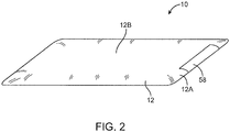
- FIG. 2 is a rear perspective view of device 10 of FIG. 1 showing how device 10 may have a relatively planar rear surface 12B and showing how dielectric antenna window 58 may be rectangular in shape with curved portions that match the shape of curved housing edges 12A (as an example).
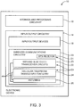
- FIG. 3 A schematic diagram of device 10 showing how device 10 may include one or more antennas 26 and transceiver circuits that communicate with antennas 26 is shown in FIG. 3 .
- electronic device 10 may include storage and processing circuitry 16.
- Storage and processing circuitry 16 may include one or more different types of storage such as hard disk drive storage, nonvolatile memory (e.g., flash memory or other electrically-programmable-read-only memory), volatile memory (e.g., static or dynamic random-access-memory), etc.
- Processing circuitry in storage and processing circuitry 16 may be used to control the operation of device 10.
- Processing circuitry 16 may be based on a processor such as a microprocessor and other suitable integrated circuits.
- storage and processing circuitry 16 may be used to run software on device 10, such as internet browsing applications, voice-over-internet-protocol (VOIP) telephone call applications, email applications, media playback applications, operating system functions, control functions for controlling radio-frequency power amplifiers and other radio-frequency transceiver circuitry, etc.
- Storage and processing circuitry 16 may be used in implementing suitable communications protocols.
- Communications protocols that may be implemented using storage and processing circuitry 16 include internet protocols, cellular telephone protocols, wireless local area network protocols (e.g., IEEE 802.11 protocols -- sometimes referred to as WiFi ® ), protocols for other short-range wireless communications links such as the Bluetooth ® protocol, etc.
- Input-output circuitry 14 may be used to allow data to be supplied to device 10 and to allow data to be provided from device 10 to external devices.
- Input-output devices 18 such as touch screens and other user input interface are examples of input-output circuitry 14.
- Input-output devices 18 may also include user input-output devices such as buttons, joysticks, click wheels, scrolling wheels, touch pads, key pads, keyboards, microphones, cameras, etc. A user can control the operation of device 10 by supplying commands through such user input devices.
- Display and audio devices may be included in devices 18 such as liquid-crystal display (LCD) screens, light-emitting diodes (LEDs), organic light-emitting diodes (OLEDs), and other components that present visual information and status data.
- Display and audio components in input-output devices 18 may also include audio equipment such as speakers and other devices for creating sound. If desired, input-output devices 18 may contain audio-video interface equipment such as jacks and other connectors for external headphones and monitors.
- Wireless communications circuitry 20 may include radio-frequency (RF) transceiver circuitry 23 formed from one or more integrated circuits, power amplifier circuitry, low-noise input amplifiers, passive RF components, one or more antennas, and other circuitry for handling RF wireless signals. Wireless signals can also be sent using light (e.g., using infrared communications).
- RF radio-frequency
- Wireless communications circuitry 20 may include radio-frequency transceiver circuits for handling multiple radio-frequency communications bands.
- circuitry 23 may include transceiver circuitry 22 that handles 2.4 GHz and 5 GHz bands for WiFi (IEEE 802.11) communications and the 2.4 GHz Bluetooth communications band.
- Circuitry 23 may also include cellular telephone transceiver circuitry 24 for handling wireless communications in cellular telephone bands such as the bands at 850 MHz, 900 MHz, 1800 MHz, and 1900 MHz, and 2100 MHz band (as examples).
- Wireless communications circuitry 20 can include circuitry for other short-range and long-range wireless links if desired.
- transceiver circuitry 23 may include global positioning system (GPS) receiver equipment 21, wireless circuitry for receiving radio and television signals, paging circuits, etc.
- GPS global positioning system
- WiFi and Bluetooth links and other short-range wireless links wireless signals are typically used to convey data over tens or hundreds of feet.
- cellular telephone links and other long-range links wireless signals are typically used to convey data over thousands of feet or miles.
- Wireless communications circuitry 20 may include antennas 26 such as an antenna or antennas located adjacent to antenna window 58 and under the inactive peripheral portion 54 of display 50.
- Antennas 26 may be single band antennas that each cover a particular desired communications band or may be multiband antennas.
- a multiband antenna may be used, for example, to cover multiple cellular telephone communications bands.
- a dual band antenna may be used to cover two WiFi bands (e.g., 2.4 GHz and 5 GHz).
- a single band antenna may be used to receive satellite navigation system signals such as Global Positioning System signals at 1575 MHz (as an example). Different types of antennas may be used for different bands and combinations of bands. For example, it may be desirable to form a dual band antenna for forming a local wireless link antenna, a multiband antenna for handling cellular telephone communications bands, and a single band antenna for forming a global positioning system antenna (as examples).
- Transmission line paths 44 may be used to convey radio-frequency signals between transceivers 23 and antennas 26.
- Radio-frequency transceivers such as radio-frequency transceivers 23 may be implemented using one or more integrated circuits and associated components (e.g., switching circuits, matching network components such as discrete inductors, capacitors, and resistors, and integrated circuit filter networks, etc.). These devices may be mounted on any suitable mounting structures. With one suitable arrangement, transceiver integrated circuits may be mounted on a printed circuit board.
- Paths 44 may be used to interconnect the transceiver integrated circuits and other components on the printed circuit board with antenna structures in device 10. Paths 44 may include any suitable conductive pathways over which radio-frequency signals may be conveyed including transmission line path structures such as coaxial cables, microstrip transmission lines, etc.
- Antennas 26 may, in general, be formed using any suitable antenna types.
- suitable antenna types for antennas 26 include antennas with resonating elements that are formed from patch antenna structures, inverted-F antenna structures, closed and open slot antenna structures, loop antenna structures, monopoles, dipoles, planar inverted-F antenna structures, hybrids of these designs, etc.
- part of housing 12 e.g., the portion of housing 12 in the vicinity of antenna window 58
- Antenna ground structures may also be formed from conductive traces on printed circuit boards, internal housing members such as frame members and structural internal housing plates, conductive portions of components such as connectors, and other conductive structures.
- antennas 26 may each include an antenna resonating element and an antenna ground.
- antenna resonating element substrate 62A includes antenna resonating element 64-1 and antenna resonating element 64-2.
- Antenna resonating elements 64-1 and 64-2 may be formed from a patterned conductor such as patterned copper, gold, or other metals.
- Substrate 62A may be formed from a flex circuit substrate such as a sheet of polyimide or another flexible polymer sheet.
- antenna resonating elements 64-1 and 64-2 form respective first and second antennas 26.
- antenna resonating element 64-3 on antenna resonating element substrate 62B may form another antenna 26 such as another cellular telephone antenna.
- Substrate 62B may be, for example, a flex circuit substrate and antenna resonating element 64-3 may be formed using a patterned metal trace on the flex circuit substrate.
- Components 60 such as a camera or other electronic component for device 10 may be interposed been substrates 62A and 62B.
- the antenna formed from antenna resonating element 64-3 may serve as a primary cellular telephone antenna for device 10 and antenna resonating element 64-1 may serve as a secondary cellular telephone antenna for device 10.
- the antenna formed from antenna resonating element 64-2 may serve as a satellite navigation system antenna such as a Global Positioning System antenna. This is merely illustrative.
- Antenna resonating elements 64-1, 64-2, and 64-3 and, if desired, additional antenna resonating elements in device 10 may be used in forming any suitable types of antennas.
- Antennas 26 may be connected to transceiver circuitry 23 (e.g., cellular telephone transceiver circuitry, satellite navigation system receiver circuitry, etc.) using transmission line paths 44.
- transceiver circuitry 23 e.g., cellular telephone transceiver circuitry, satellite navigation system receiver circuitry, etc.
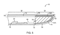
- FIG. 5 A cross-sectional side view of housing 12 of device 10 showing how antenna resonating element substrate 62A may be mounted under the surface of cover glass layer 68 in display 50 is shown in FIG. 5 .
- display 50 may include a display module (e.g., a liquid crystal display module or an organic light-emitting display module such as module 72 in active area 56).
- a layer of opaque material 66 such as black ink may hide antenna resonating element substrate 62A from view by a user of device 10.
- the antenna resonating elements on substrate 62A may be fed using respective antenna feeds and may form respective first and second antennas.
- FIG. 5 shows how each transmission line 44 in device 10 may have be coupled to a respective antenna using a respective antenna feed that has a positive antenna feed terminal such as terminal 76 and a ground antenna feed terminal such as terminal 78.
- Positive antenna feed terminals 76 may be coupled to traces on the antenna resonating element substrates.
- Ground antenna feed terminals may be coupled to conductive antenna ground structures such as housing structure 12.
- Transmission lines 44 may couple feed terminals 76 and 78 to radio-frequency transceiver circuitry 23 on printed circuit board 79.
- Antenna resonating element substrate 62A may be wrapped around a dielectric carrier such as carrier 70.
- Carrier 70 may be formed from any suitable dielectric material (e.g., a plastic such as a liquid crystal polymer or other suitable dielectric).
- carrier 70 may have opposing planar and curved surfaces.
- the planar upper surface of carrier 70 may be mounted against the planar inner surface of display cover glass 68.
- the curved lower surface of carrier 70 may be mounted against the mating curved surface of dielectric window 58.
- Other suitable configurations for carrier 70 may be used if desired.
- Antenna resonating element substrate 62A may, if desired, be attached to carrier 70 using adhesive (e.g., pressure sensitive adhesive).
- FIG. 7 is a rear perspective view of carrier 70.
- substrate 62A may be provided with features that help couple transmission lines 44 to the first and second antennas associated with carrier 70.
- substrate 62A may have a protrusion having a resonating element trace with a first opening such as opening 86-1.
- Screw 82-1 may pass through opening 86-1 and may screw into mating screw hole 80-1 in housing portion 12" to ground the trace and form ground antenna terminal 78-1 for the first antenna (e.g., the cellular telephone antenna).
- a parasitic antenna resonating element that is used to provide the cellular telephone antenna with high band coverage may be coupled to terminal 92. When mounted in device 10, terminal 92 may be grounded to conductive housing portion 12'.
- Substrate 62A may also have a protrusion with a resonating element trace that has a second opening such as opening 86-2.
- Screw 82-2 may pass through opening 86-2 and may screw into mating screw hole 80-2 in housing portion 12" to ground the trace and form ground antenna terminal 78-2 for the second antenna (e.g., the satellite navigation system antenna).
- Air-filled cavities in carrier 70 such as cavities 84 may facilitate formation of carrier 70 using injection molding techniques.
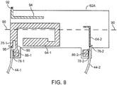
- FIG. 8 is a top view of an unwrapped version of substrate 62A, before substrate 62A is mounted to carrier 70. During mounting, substrate 62A is bent along longitudinal axis 90 and is wrapped around carrier 70 so as to cover the planar and curved surfaces of carrier 70.
- substrate 62A may have an elongated metal trace that forms antenna resonating element 64-2.
- Antenna resonating element 64-2 may be used to form a satellite navigation antenna resonating element for a satellite navigation antenna (e.g., a Global Positioning System antenna operating at 1575 MHz).
- Terminal 76-2 may be coupled to one end of the trace for antenna resonating element 64-2.
- Transmission line 44-1 may have a positive conductor that is coupled to terminal 76-2 and a ground conductor that is coupled to ground terminal 78-2 and the trace on the protruding portion of flex circuit substrate 62A that includes hole 86-2.
- substrate 62A may have a second antenna resonating element trace that is used to form antenna resonating element 64-1.
- Antenna resonating element 64-1 may be associated with a cellular telephone antenna such as a dual band cellular telephone antenna for receiving voice and non-voice wireless data over cellular telephone networks.
- Positive antenna feed terminal 76-1 may be coupled to leg 96 of antenna resonating element 64-2.
- Transmission line 44-1 may have a positive conductor that is coupled to terminal 76-1.
- Transmission line 44-1 may also have a ground conductor that is coupled to ground terminal 78-1.
- Ground terminal 78-1 may be formed from the portion of antenna resonating element 64-1 at the end of leg 98 that contains hole 86-1.
- Parasitic antenna resonating element 94 may be formed from a strip of conductor (i.e., a patterned metal trace) that is electrically isolated from trace 64-1 on substrate 62A and that is not directly feed by one of transmission lines 44-1 and 44-2. One end of parasitic antenna resonating element 94 may be grounded to housing 12 (i.e., housing portion 12' of FIG. 7 ) at terminal 92.
- FIG. 9 A graph of the response of the antennas formed using the antenna structures of FIG. 8 is shown in FIG. 9 .
- standing wave ratio SWR
- Solid line 100 shows the response of the cellular telephone antenna formed using antenna resonating element 64-1 and parasitic antenna resonating element 94. As shown by line 100, this antenna may exhibit resonant peaks in a low frequency band centered at frequency f1 (e.g., 850 MHz or 700 MHz or 900 MHz) and a high frequency band centered at frequency f2 (e.g., 1900 MHz or 1800 MHz or 2100 MHz).
- f1 e.g., 850 MHz or 700 MHz or 900 MHz
- a high frequency band centered at frequency f2 e.g., 1900 MHz or 1800 MHz or 2100 MHz.
- Dashed line 104 shows how the response of antenna resonating element 64-1 may be poor in the high-band associated with frequency f2 in the absence of parasitic antenna resonating element 94.
- the cellular telephone antenna may exhibit satisfactory response at frequency f2, as illustrated by solid line 100.
- Line 102 illustrates the response of the second antenna formed on substrate 64A (i.e., the Global Positioning System antenna formed using trace 64-2 of FIG. 8 ).
- substrate 62A may be formed on substrate 62A.
- substrate 62A include a cellular telephone antenna and a Global Positioning System antenna
- the present example involves an arrangement in which first and second antennas have first and second antenna resonating elements that are formed at longitudinally opposing ends of a common wrapped flex circuit substrate.
- a common flex circuit antenna resonating element substrate may be used to form three or more antenna resonating elements for three or more respective antennas.
Abstract
Description
- This application claims priority to United States patent application No.
13/038,300, filed March 1, 2011 - This relates generally to antennas, and, more particularly, to antennas for electronic devices.
- Electronic devices such as portable computers and handheld electronic devices are often provided with wireless communications capabilities. For example, electronic devices may use long-range wireless communications circuitry such as cellular telephone circuitry and short-range communications circuitry such as wireless local area network communications circuitry. Some devices are provided with the ability to receive other wireless signals such as Global Positioning System signals.
- It can be difficult to incorporate antennas successfully into an electronic device. Some electronic devices are manufactured with small form factors, so space for antennas is limited. In many electronic devices, the presence of electronic components in the vicinity of an antenna serves as a possible source of electromagnetic interference. Antenna operation can also be disrupted by nearby conductive structures. Considerations such as these can make it difficult to implement an antenna in an electronic device that contains conductive housing walls or other conductive structures that can potentially block radio-frequency signals.
- It would therefore be desirable to be able to provide improved antennas for wireless electronic devices.
- Antennas may be provided for electronic devices such as portable computers. A flexible antenna resonating element substrate may be wrapped around a dielectric carrier. The dielectric carrier may have first and second opposing surfaces that are covered by the wrapped substrate. The first surface may be a planar surface that is mounted against a display cover glass layer. The second surface may be a curved surface having a shape that matches a curved dielectric antenna window shape in a curved portion of the housing of an electronic device.
- The flexible antenna resonating element substrate may have a first antenna resonating element at one end and a second antenna resonating element at an opposing end. Conductive structures such as conductive housing structures may form antenna ground. The first antenna resonating element and the antenna ground may form a first antenna such as a cellular telephone antenna or other suitable antenna. The second antenna resonating element and the antenna ground may form a second antenna such as a satellite navigation system antenna or other suitable antenna.
- A parasitic antenna resonating element may form part of the first antenna. The first antenna may be configured to operate in first and second communications bands. The parasitic antenna resonating element may be used to ensure that the antenna covers the second communications band.
- Further features of the invention, its nature and various advantages will be more apparent from the accompanying drawings and the following detailed description of the preferred embodiments.
-
-
FIG. 1 is a front perspective view of an illustrative electronic device with antennas in accordance with an embodiment of the present invention. -
FIG. 2 is a rear perspective view of an illustrative electronic device with antennas in accordance with an embodiment of the present invention. -
FIG. 3 is a schematic diagram of an illustrative electronic device with antennas in accordance with an embodiment of the present invention. -
FIG. 4 is a rear view of an illustrative electronic device having antennas in accordance with an embodiment of the present invention. -
FIG. 5 is a cross-sectional side view of an illustrative electronic device with antennas in accordance with an embodiment of the present invention. -
FIG. 6 is a perspective view of an antenna resonating element substrate wrapped around a carrier in accordance with an embodiment of the present invention. -
FIG. 7 is an exploded perspective view showing housing portions and fasteners that may be used in mounting an antenna resonating element substrate and carrier within an electronic device in accordance with an embodiment of the present invention. -
FIG. 8 is a top view of an unwrapped antenna resonating element substrate of the type shown inFIG. 6 and 7 showing an illustrative pattern of conductive antenna traces that may be used in forming a pair of antennas in accordance with an embodiment of the present invention. -
FIG. 9 is a graph in which the standing-wave-ratio for an illustrative pair of antennas such as a cellular telephone antenna and satellite navigation system antenna formed on a substrate of the type shown inFIG. 8 have been plotted as a function of operating frequency in accordance with an embodiment of the present invention. - Electronic devices may be provided with wireless communications circuitry. The wireless communications circuitry may be used to support wireless communications in one or more wireless communications bands. For example, the wireless communications circuitry may transmit and receive signals in cellular telephone bands and other communications bands and may receive wireless signals in satellite navigation system bands.
- Space is at a premium in electronic devices such as portable electronic devices. Housings for these devices are sometimes constructed from conductive materials that block antenna signals. Arrangements in which antenna structures are formed behind a dielectric antenna window can help address these challenges. A dielectric window may be formed within an opening in the conductive housing wall. If desired, wireless signals can also be accommodate by forming all or most of an electronic device housing from a dielectric such as plastic. In some configurations, wireless signals can pass through dielectric structures such as the cover glass layers associated with a display. These configurations, other configurations for accommodating wireless signals in a device, or combinations of these configurations may be used in a wireless electronic device if desired.
- Antenna resonating elements for antennas may be formed in the vicinity of an antenna window and under a portion of a display cover layer. Portions of a conductive housing or other conductive structures may serve as antenna ground. The antenna can be fed using a positive antenna feed terminal that is coupled to the antenna resonating element and a ground antenna feed terminal that is coupled to the conductive housing. During operation, radio-frequency signals for the antenna can pass through the antenna window and other non-conducting housing structures such as part of the cover glass.
- The antennas may be formed from antenna resonating elements and conductive portions of the housing or other conductive structures that serve as antenna ground. The antenna resonating elements may be formed from conductive traces on a dielectric substrate. The conductive traces may be formed from copper or other metals. The dielectric substrate may be, for example, a flexible printed circuit. Flexible printed circuits, which are sometimes referred to as flex circuits, have conductive traces formed on a flexible dielectric substrate such as sheets of polyimide or other polymers.
- The antenna resonating element substrate may be mounted on a support structure. For example, a flexible antenna resonating element substrate that includes multiple antenna resonating elements for multiple antennas may be wrapped around a dielectric carrier such as a molded plastic carrier or other plastic support structure. Wrapping the antenna resonating substrate around the carrier in this way allows the antennas to be efficiently mounted within a small available housing volume.
- Antenna structures with configurations such as these can be mounted on any suitable exposed portion of a portable electronic device. For example, antennas can be provided on the front or top surface of the device. In a tablet computer, cellular telephone, or other device in which the front of the device is all or mostly occupied with conductive structures such as a touch screen display, it may be desirable to form at least part of the antenna window on a rear device surface. Other configurations are also possible (e.g., with antennas mounted in more confined locations, on device sidewalls, etc.). The use of antenna mounting locations in which at least part of a dielectric antenna window is formed in a conductive rear housing surface is sometimes described herein as an example, but, in general, any suitable antenna mounting location may be used in an electronic device if desired.
- An illustrative portable device that may include antenna structures with resonating element substrates that are wrapped around a carrier is shown in
FIG. 1 . In general, devices such asdevice 10 ofFIG. 1 may be any suitable electronic devices with wireless communications capabilities such as desktop computers, portable computers such as laptop computers and tablet computers, handheld electronic devices such as cellular telephones, smaller portable electronic devices such as wrist-watch devices, pendant devices, headphone devices, and earpiece devices, or other wearable or miniature devices. - As shown in
FIG. 1 ,device 10 may be a relatively thin device such as a tablet computer.Device 10 may have display such asdisplay 50 mounted on its front (top) surface.Housing 12 may have curved portions that form the edges ofdevice 10 and a relatively planar portion that forms the rear surface of device 10 (as an example). Housings with straight sidewalls and other configurations may also be used. The front surface of device 10 (i.e., the cover of display 50) may sometimes be referred to as forming the front housing surface ofdevice 12. - The cover of
display 50 may be formed from a layer of cover glass, a layer of plastic, or other materials. The cover layer fordisplay 50 may be radio transparent in its inactive edge region (i.e., away from the conductive portions of the display that include active pixel circuits). As a result, radio-frequency signals may be received by antenna structures that are mounted under an edge portion of the display cover layer and may be transmitted from the antenna structures through the edge portion of the display cover layer. In configurations in whichhousing 12 is formed form a metal or other conductive material, a dielectric window such asdielectric window 58 may be formed inhousing 12. Antenna structures fordevice 10 may be formed in the vicinity ofdielectric window 58, so that radio-frequency antenna signals can pass throughdielectric window 58 in addition to or instead of passing through the edge portions of the display cover layer. -
Device 10 may have user input-output devices such asbutton 59.Display 50 may be a touch screen display that is used in gathering user touch input. Capacitive touch sensors or other touch sensors for the display may be implemented using a touch panel that is mounted under a planar cover glass member on the surface ofdisplay 50, may be integrated onto the cover glass layer, or may be otherwise incorporated intodisplay 50. - The central portion of display 50 (shown as
region 56 inFIG. 1 ) may be an active region that is sensitive to touch input and that is used in displaying images to a user using an array of image pixels (e.g., liquid crystal display image pixels, organic light-emitting diode image pixels, or other display pixels). The peripheral regions ofdisplay 50 such asregions 54 may be inactive regions that are free from touch sensor electrodes and image pixels. A layer of material such as an opaque ink may be placed on the underside ofdisplay 50 in peripheral regions 54 (e.g., on the underside of the cover glass). This layer may be transparent to radio-frequency signals. The conductive touch sensor electrodes inregion 56 and the conductive structures associated with the array of image pixels in the display may tend to block radio-frequency signals. However, radio-frequency signals may pass through the cover glass and opaque ink in inactive display regions 54 (as an example). Radio-frequency signals may also pass throughantenna window 58. -
Housing 12 may be formed from one or more structures. For example,housing 12 may include an internal frame and planar housing walls that are mounted to the frame.Housing 12 may also be formed from a unitary block of material such as a cast or machined block of aluminum. Arrangements that use both of these approaches may also be used if desired. -
Housing 12 may be formed of any suitable materials including plastic, wood, glass, ceramics, metal, or other suitable materials, or a combination of these materials. In some situations, portions ofhousing 12 may be formed from a dielectric or other low-conductivity material, so as not to disturb the operation of conductive antenna elements that are located in proximity tohousing 12. In other situations,housing 12 may be formed from metal elements. An advantage of forminghousing 12 from metal or other structurally sound conductive materials is that this may improve device aesthetics and may help improve durability and portability. - With one suitable arrangement,
housing 12 may be formed from a metal such as aluminum or stainless steel. Portions ofhousing 12 in the vicinity ofantenna window 58 may serve as antenna ground.Antenna window 58 may be formed from a dielectric material such as polycarbonate (PC), acrylonitrile butadiene styrene (ABS), a PC/ABS blend, or other plastics (as examples).Window 58 may be attached tohousing 12 using adhesive, fasteners, or other suitable attachment mechanisms. To ensure thatdevice 10 has an attractive appearance, it may be desirable to formwindow 58 so that the exterior surfaces ofwindow 58 conform to the edge profile exhibited byhousing 12 in other portions ofdevice 10. For example, ifhousing 12 hasstraight edges 12A and a flat bottom surface,window 58 may be formed with a right-angle bend and vertical sidewalls. Ifhousing 12 hascurved edges 12A,window 58 may have a similarly curved surface. -
FIG. 2 is a rear perspective view ofdevice 10 ofFIG. 1 showing howdevice 10 may have a relatively planarrear surface 12B and showing howdielectric antenna window 58 may be rectangular in shape with curved portions that match the shape ofcurved housing edges 12A (as an example). - A schematic diagram of
device 10 showing howdevice 10 may include one ormore antennas 26 and transceiver circuits that communicate withantennas 26 is shown inFIG. 3 . As shown inFIG. 3 ,electronic device 10 may include storage andprocessing circuitry 16. Storage andprocessing circuitry 16 may include one or more different types of storage such as hard disk drive storage, nonvolatile memory (e.g., flash memory or other electrically-programmable-read-only memory), volatile memory (e.g., static or dynamic random-access-memory), etc. Processing circuitry in storage andprocessing circuitry 16 may be used to control the operation ofdevice 10.Processing circuitry 16 may be based on a processor such as a microprocessor and other suitable integrated circuits. With one suitable arrangement, storage andprocessing circuitry 16 may be used to run software ondevice 10, such as internet browsing applications, voice-over-internet-protocol (VOIP) telephone call applications, email applications, media playback applications, operating system functions, control functions for controlling radio-frequency power amplifiers and other radio-frequency transceiver circuitry, etc. Storage andprocessing circuitry 16 may be used in implementing suitable communications protocols. Communications protocols that may be implemented using storage andprocessing circuitry 16 include internet protocols, cellular telephone protocols, wireless local area network protocols (e.g., IEEE 802.11 protocols -- sometimes referred to as WiFi®), protocols for other short-range wireless communications links such as the Bluetooth® protocol, etc. - Input-
output circuitry 14 may be used to allow data to be supplied todevice 10 and to allow data to be provided fromdevice 10 to external devices. Input-output devices 18 such as touch screens and other user input interface are examples of input-output circuitry 14. Input-output devices 18 may also include user input-output devices such as buttons, joysticks, click wheels, scrolling wheels, touch pads, key pads, keyboards, microphones, cameras, etc. A user can control the operation ofdevice 10 by supplying commands through such user input devices. Display and audio devices may be included indevices 18 such as liquid-crystal display (LCD) screens, light-emitting diodes (LEDs), organic light-emitting diodes (OLEDs), and other components that present visual information and status data. Display and audio components in input-output devices 18 may also include audio equipment such as speakers and other devices for creating sound. If desired, input-output devices 18 may contain audio-video interface equipment such as jacks and other connectors for external headphones and monitors. -
Wireless communications circuitry 20 may include radio-frequency (RF)transceiver circuitry 23 formed from one or more integrated circuits, power amplifier circuitry, low-noise input amplifiers, passive RF components, one or more antennas, and other circuitry for handling RF wireless signals. Wireless signals can also be sent using light (e.g., using infrared communications). -
Wireless communications circuitry 20 may include radio-frequency transceiver circuits for handling multiple radio-frequency communications bands. For example,circuitry 23 may includetransceiver circuitry 22 that handles 2.4 GHz and 5 GHz bands for WiFi (IEEE 802.11) communications and the 2.4 GHz Bluetooth communications band.Circuitry 23 may also include cellulartelephone transceiver circuitry 24 for handling wireless communications in cellular telephone bands such as the bands at 850 MHz, 900 MHz, 1800 MHz, and 1900 MHz, and 2100 MHz band (as examples).Wireless communications circuitry 20 can include circuitry for other short-range and long-range wireless links if desired. For example,transceiver circuitry 23 may include global positioning system (GPS)receiver equipment 21, wireless circuitry for receiving radio and television signals, paging circuits, etc. In WiFi and Bluetooth links and other short-range wireless links, wireless signals are typically used to convey data over tens or hundreds of feet. In cellular telephone links and other long-range links, wireless signals are typically used to convey data over thousands of feet or miles. -
Wireless communications circuitry 20 may includeantennas 26 such as an antenna or antennas located adjacent toantenna window 58 and under the inactiveperipheral portion 54 ofdisplay 50.Antennas 26 may be single band antennas that each cover a particular desired communications band or may be multiband antennas. A multiband antenna may be used, for example, to cover multiple cellular telephone communications bands. If desired, a dual band antenna may be used to cover two WiFi bands (e.g., 2.4 GHz and 5 GHz). A single band antenna may be used to receive satellite navigation system signals such as Global Positioning System signals at 1575 MHz (as an example). Different types of antennas may be used for different bands and combinations of bands. For example, it may be desirable to form a dual band antenna for forming a local wireless link antenna, a multiband antenna for handling cellular telephone communications bands, and a single band antenna for forming a global positioning system antenna (as examples). -
Transmission line paths 44 may be used to convey radio-frequency signals betweentransceivers 23 andantennas 26. Radio-frequency transceivers such as radio-frequency transceivers 23 may be implemented using one or more integrated circuits and associated components (e.g., switching circuits, matching network components such as discrete inductors, capacitors, and resistors, and integrated circuit filter networks, etc.). These devices may be mounted on any suitable mounting structures. With one suitable arrangement, transceiver integrated circuits may be mounted on a printed circuit board.Paths 44 may be used to interconnect the transceiver integrated circuits and other components on the printed circuit board with antenna structures indevice 10.Paths 44 may include any suitable conductive pathways over which radio-frequency signals may be conveyed including transmission line path structures such as coaxial cables, microstrip transmission lines, etc. -
Antennas 26 may, in general, be formed using any suitable antenna types. Examples of suitable antenna types forantennas 26 include antennas with resonating elements that are formed from patch antenna structures, inverted-F antenna structures, closed and open slot antenna structures, loop antenna structures, monopoles, dipoles, planar inverted-F antenna structures, hybrids of these designs, etc. With one suitable arrangement, which is sometimes described herein as an example, part of housing 12 (e.g., the portion ofhousing 12 in the vicinity of antenna window 58) may form a ground structure for the antenna associated withwindow 58. Antenna ground structures may also be formed from conductive traces on printed circuit boards, internal housing members such as frame members and structural internal housing plates, conductive portions of components such as connectors, and other conductive structures. - A rear view of
electronic device 10 in the vicinity ofdielectric window 58 is shown inFIG. 4 . As shown inFIG. 4 ,antennas 26 may each include an antenna resonating element and an antenna ground. In the example ofFIG. 4 , antenna resonatingelement substrate 62A includes antenna resonating element 64-1 and antenna resonating element 64-2. Antenna resonating elements 64-1 and 64-2 may be formed from a patterned conductor such as patterned copper, gold, or other metals.Substrate 62A may be formed from a flex circuit substrate such as a sheet of polyimide or another flexible polymer sheet. In conjunction with nearby conductive structures such as portions ofhousing 12 or other ground structures that serve as antenna ground, antenna resonating elements 64-1 and 64-2 form respective first andsecond antennas 26. - At the lower portion of
antenna window 58 in the example ofFIG. 4 , antenna resonating element 64-3 on antenna resonatingelement substrate 62B may form anotherantenna 26 such as another cellular telephone antenna.Substrate 62B may be, for example, a flex circuit substrate and antenna resonating element 64-3 may be formed using a patterned metal trace on the flex circuit substrate.Components 60 such as a camera or other electronic component fordevice 10 may be interposed beensubstrates - With one suitable arrangement, the antenna formed from antenna resonating element 64-3 may serve as a primary cellular telephone antenna for
device 10 and antenna resonating element 64-1 may serve as a secondary cellular telephone antenna fordevice 10. The antenna formed from antenna resonating element 64-2 may serve as a satellite navigation system antenna such as a Global Positioning System antenna. This is merely illustrative. Antenna resonating elements 64-1, 64-2, and 64-3 and, if desired, additional antenna resonating elements indevice 10 may be used in forming any suitable types of antennas. -
Antennas 26 may be connected to transceiver circuitry 23 (e.g., cellular telephone transceiver circuitry, satellite navigation system receiver circuitry, etc.) usingtransmission line paths 44. - A cross-sectional side view of
housing 12 ofdevice 10 showing how antenna resonatingelement substrate 62A may be mounted under the surface ofcover glass layer 68 indisplay 50 is shown inFIG. 5 . As shown inFIG. 5 ,display 50 may include a display module (e.g., a liquid crystal display module or an organic light-emitting display module such asmodule 72 in active area 56). Ininactive area 54, a layer ofopaque material 66 such as black ink may hide antenna resonatingelement substrate 62A from view by a user ofdevice 10. - The antenna resonating elements on
substrate 62A (i.e., antenna resonating elements 64-1 and 64-2 ofFIG. 4 ) may be fed using respective antenna feeds and may form respective first and second antennas.FIG. 5 shows how eachtransmission line 44 indevice 10 may have be coupled to a respective antenna using a respective antenna feed that has a positive antenna feed terminal such asterminal 76 and a ground antenna feed terminal such asterminal 78. Positiveantenna feed terminals 76 may be coupled to traces on the antenna resonating element substrates. Ground antenna feed terminals may be coupled to conductive antenna ground structures such ashousing structure 12.Transmission lines 44 may couplefeed terminals frequency transceiver circuitry 23 on printedcircuit board 79. - Antenna resonating
element substrate 62A may be wrapped around a dielectric carrier such ascarrier 70.Carrier 70 may be formed from any suitable dielectric material (e.g., a plastic such as a liquid crystal polymer or other suitable dielectric). In housing configurations of the type shown inFIG. 5 in which a portion of the housing (i.e., antenna window 58) is curved,carrier 70 may have opposing planar and curved surfaces. The planar upper surface ofcarrier 70 may be mounted against the planar inner surface ofdisplay cover glass 68. The curved lower surface ofcarrier 70 may be mounted against the mating curved surface ofdielectric window 58. In housings with other shapes, other suitable configurations forcarrier 70 may be used if desired. Antenna resonatingelement substrate 62A may, if desired, be attached tocarrier 70 using adhesive (e.g., pressure sensitive adhesive). - A front perspective view of
carrier 70 showing how the curved lower surface and the opposing planar upper surface of the carrier may meet along a common axis (axis 90) that runs along the peripheral upper edge ofdevice 10 is shown inFIG. 6 . -
FIG. 7 is a rear perspective view ofcarrier 70. A shown inFIG. 7 ,substrate 62A may be provided with features that helpcouple transmission lines 44 to the first and second antennas associated withcarrier 70. In particular,substrate 62A may have a protrusion having a resonating element trace with a first opening such as opening 86-1. Screw 82-1 may pass through opening 86-1 and may screw into mating screw hole 80-1 inhousing portion 12" to ground the trace and form ground antenna terminal 78-1 for the first antenna (e.g., the cellular telephone antenna). A parasitic antenna resonating element that is used to provide the cellular telephone antenna with high band coverage may be coupled toterminal 92. When mounted indevice 10, terminal 92 may be grounded to conductive housing portion 12'.Substrate 62A may also have a protrusion with a resonating element trace that has a second opening such as opening 86-2. Screw 82-2 may pass through opening 86-2 and may screw into mating screw hole 80-2 inhousing portion 12" to ground the trace and form ground antenna terminal 78-2 for the second antenna (e.g., the satellite navigation system antenna). - Air-filled cavities in
carrier 70 such ascavities 84 may facilitate formation ofcarrier 70 using injection molding techniques. -
FIG. 8 is a top view of an unwrapped version ofsubstrate 62A, beforesubstrate 62A is mounted tocarrier 70. During mounting,substrate 62A is bent alonglongitudinal axis 90 and is wrapped aroundcarrier 70 so as to cover the planar and curved surfaces ofcarrier 70. - As shown in
FIG. 8 ,substrate 62A may have an elongated metal trace that forms antenna resonating element 64-2. Antenna resonating element 64-2 may be used to form a satellite navigation antenna resonating element for a satellite navigation antenna (e.g., a Global Positioning System antenna operating at 1575 MHz). Terminal 76-2 may be coupled to one end of the trace for antenna resonating element 64-2. Transmission line 44-1 may have a positive conductor that is coupled to terminal 76-2 and a ground conductor that is coupled to ground terminal 78-2 and the trace on the protruding portion offlex circuit substrate 62A that includes hole 86-2. - At the opposing end of
substrate 62A (i.e., the left-hand end in the configuration ofFIG. 8 ),substrate 62A may have a second antenna resonating element trace that is used to form antenna resonating element 64-1. Antenna resonating element 64-1 may be associated with a cellular telephone antenna such as a dual band cellular telephone antenna for receiving voice and non-voice wireless data over cellular telephone networks. Positive antenna feed terminal 76-1 may be coupled toleg 96 of antenna resonating element 64-2. Transmission line 44-1 may have a positive conductor that is coupled to terminal 76-1. Transmission line 44-1 may also have a ground conductor that is coupled to ground terminal 78-1. Ground terminal 78-1 may be formed from the portion of antenna resonating element 64-1 at the end ofleg 98 that contains hole 86-1. - Parasitic
antenna resonating element 94 may be formed from a strip of conductor (i.e., a patterned metal trace) that is electrically isolated from trace 64-1 onsubstrate 62A and that is not directly feed by one of transmission lines 44-1 and 44-2. One end of parasiticantenna resonating element 94 may be grounded to housing 12 (i.e., housing portion 12' ofFIG. 7 ) atterminal 92. - A graph of the response of the antennas formed using the antenna structures of
FIG. 8 is shown inFIG. 9 . In the graph ofFIG. 9 , standing wave ratio (SWR) has been plotted as a function of operating frequency.Solid line 100 shows the response of the cellular telephone antenna formed using antenna resonating element 64-1 and parasiticantenna resonating element 94. As shown byline 100, this antenna may exhibit resonant peaks in a low frequency band centered at frequency f1 (e.g., 850 MHz or 700 MHz or 900 MHz) and a high frequency band centered at frequency f2 (e.g., 1900 MHz or 1800 MHz or 2100 MHz). Dashedline 104 shows how the response of antenna resonating element 64-1 may be poor in the high-band associated with frequency f2 in the absence of parasiticantenna resonating element 94. When parasiticantenna resonating element 94 is present, however, the cellular telephone antenna may exhibit satisfactory response at frequency f2, as illustrated bysolid line 100.Line 102 illustrates the response of the second antenna formed on substrate 64A (i.e., the Global Positioning System antenna formed using trace 64-2 ofFIG. 8 ). - If desired, other types of antennas may be formed on
substrate 62A. The illustrative arrangement ofFIGS. 8 and9 in whichsubstrate 62A include a cellular telephone antenna and a Global Positioning System antenna is merely illustrative. Moreover, there may be more than two separate antennas formed on a common wrapped flex circuit substrate. The present example involves an arrangement in which first and second antennas have first and second antenna resonating elements that are formed at longitudinally opposing ends of a common wrapped flex circuit substrate. If desired, a common flex circuit antenna resonating element substrate may be used to form three or more antenna resonating elements for three or more respective antennas. - The invention can also be defined as shown in the following clauses:
- 1. An electronic device antenna structure, comprising:
- a plastic support structure having opposing first and second surfaces; and
- an antenna resonating element substrate having first and second antenna resonating elements for first and second respective antennas, wherein the antenna resonating element substrate is wrapped around the plastic support structure and covers the first and second surfaces.
- 2. The electronic device antenna structure defined in
clause 1 further comprising a parasitic antenna resonating element on the antenna resonating element substrate that forms part of the first antenna. - 3. The electronic device antenna structure defined in clause 2 wherein the parasitic antenna resonating element structure comprises a strip of conductor having a terminal that is connected to an electronic device housing.
- 4. The electronic device antenna structure defined in clause 2 wherein the first antenna is configured to operate in first and second cellular telephone communications bands.
- 5. The electronic device antenna structure defined in clause 4 wherein the second antenna is configured to operate in a satellite navigation system band.
- 6. The electronic device antenna structure defined in
clause 1 wherein the first surface comprises a planar surface, wherein the second surface comprises a curved surface, and wherein the antenna resonating element substrate comprises a flexible sheet of polymer that is attached with adhesive to the first and second surfaces. - 7. The electronic device antenna structure defined in
clause 1 wherein the first and second surfaces meet along an axis and wherein the antenna resonating element substrate is bent along the axis. - 8. The electronic device antenna structure defined in clause 7 wherein the axis runs along a longitudinal dimension of the antenna resonating element substrate, wherein the antenna resonating element substrate has first and second longitudinally opposing ends, wherein the first antenna resonating element is located at the first and, and wherein the second antenna resonating element is located at the second end.
- 9. An electronic device, comprising:
- a dielectric carrier having opposing first and second surfaces;
- a flexible antenna resonating element substrate that covers at least some of the first and second surfaces;
- a conductive housing that forms an antenna ground;
- a first antenna resonating element on the flexible antenna resonating element substrate, wherein the antenna ground and the first antenna resonating element form a first antenna; and
- a second antenna resonating element on the flexible antenna resonating element substrate, wherein the antenna ground and the second antenna resonating element form a second antenna.
- 10. The electronic device defined in clause 9 further comprising a dielectric window in the conductive housing, wherein the carrier is mounted adjacent to the dielectric window.
- 11. The electronic device defined in
clause 10 further comprising a display with a cover glass layer, wherein the carrier is mounted adjacent to the cover glass layer. - 12. The electronic device defined in clause 11 wherein the first surface comprises a planar surface and wherein the dielectric carrier is mounted so that the planar surface lies against the cover glass layer.
- 13. The electronic device defined in
clause 12 wherein the display has an active area that is surrounded by a peripheral inactive area, wherein an inner surface of the cover glass layer in the peripheral inactive area is peripheral inactive area is covered with an opaque masking layer, and wherein the planar surface is covered by the opaque masking layer. - 14. The electronic device defined in clause 13 wherein the dielectric window has a curved shape and wherein the second surface is curved to match the curved shape of the dielectric window.
- 15. The electronic device defined in clause 9 further comprising a parasitic antenna resonating element on the flexible antenna resonating element substrate adjacent to the first antenna resonating element, wherein the parasitic antenna resonating element forms part of the first antenna.
- 16. The electronic device defined in clause 15 further comprising a display cover glass layer and a dielectric window, wherein the dielectric carrier is interposed between the display cover glass and the dielectric window so that radio-frequency signals are received by the first and second antennas through the display cover glass and the dielectric window.
- 17. Apparatus, comprising:
- a dielectric carrier; and
- a flexible antenna resonating element substrate wrapped around the dielectric carrier and having first and second antenna resonating elements that form first and second antennas.
- 18. The apparatus defined in clause 17 wherein the dielectric carrier has first and second surfaces that meet along an axis, wherein the flexible antenna resonating substrate is bent over the carrier along the axis, and wherein the flexible antenna resonating element substrate covers the first and second surfaces.
- 19. The apparatus defined in
clause 18 further comprising a parasitic antenna resonating element on the flexible antenna resonating element substrate that forms part of the first antenna. - 20. The apparatus defined in clause 19 wherein the first antenna is configured to operate in at least two cellular telephone communications bands and wherein the second antenna is configured to operate in a satellite navigation system band.
- The foregoing is merely illustrative of the principles of this invention and various modifications can be made by those skilled in the art without departing from the scope and spirit of the invention.
Claims (14)
- An electronic device, comprising:a dielectric carrier having opposing first and second surfaces;a flexible antenna resonating element substrate that covers at least some of the first and second surfaces;a conductive housing that forms an antenna ground;a first antenna resonating element on the flexible antenna resonating element substrate, wherein the antenna ground and the first antenna resonating element form a first antenna; anda second antenna resonating element on the flexible antenna resonating element substrate, wherein the antenna ground and the second antenna resonating element form a second antenna.
- The electronic device defined in claim 1 further comprising a dielectric window in the conductive housing, wherein the carrier is mounted adjacent to the dielectric window.
- The electronic device defined in claim 2 further comprising a display with a cover glass layer, wherein the carrier is mounted adjacent to the cover glass layer.
- The electronic device defined in claim 3 wherein the first surface comprises a planar surface and wherein the dielectric carrier is mounted so that the planar surface lies against the cover glass layer.
- The electronic device defined in claim 4 wherein the display has an active area that is surrounded by a peripheral inactive area, wherein an inner surface of the cover glass layer in the peripheral inactive area is peripheral inactive area is covered with an opaque masking layer, and wherein the planar surface is covered by the opaque masking layer.
- The electronic device defined in claim 5 wherein the dielectric window has a curved shape and wherein the second surface is curved to match the curved shape of the dielectric window.
- The electronic device defined in claim 1 further comprising a parasitic antenna resonating element on the flexible antenna resonating element substrate adjacent to the first antenna resonating element, wherein the parasitic antenna resonating element forms part of the first antenna.
- The electronic device defined in claim 7 further comprising a display cover glass layer and a dielectric window, wherein the dielectric carrier is interposed between the display cover glass and the dielectric window so that radio-frequency signals are received by the first and second antennas through the display cover glass and the dielectric window.
- The electronic device defined in claim 7 wherein the parasitic antenna resonating element comprises a strip of conductor having a terminal that is connected to the conductive housing.
- The electronic device defined in claim 1 wherein the first antenna is configured to operate in first and second cellular telephone communications bands.
- The electronic device defined in claim 1 wherein the second antenna is configured to operate in a satellite navigation system band.
- The electronic device defined in claim 1 wherein the first surface comprises a planar surface, wherein the second surface comprises a curved surface, and wherein the flexible antenna resonating element substrate comprises a flexible sheet of polymer that is attached with adhesive to the first and second surfaces.
- The electronic device defined in claim 1 wherein the first and second surfaces meet along an axis and wherein the flexible antenna resonating element substrate is bent along the axis.
- The electronic device defined in claim 13 wherein the axis runs along a longitudinal dimension of the flexible antenna resonating element substrate, wherein the flexible antenna resonating element substrate has first and second longitudinally opposing ends, wherein the first antenna resonating element is located at the first and, and wherein the second antenna resonating element is located at the second end.
Applications Claiming Priority (1)
| Application Number | Priority Date | Filing Date | Title |
|---|---|---|---|
| US13/038,300 US8896488B2 (en) | 2011-03-01 | 2011-03-01 | Multi-element antenna structure with wrapped substrate |
Publications (3)
| Publication Number | Publication Date |
|---|---|
| EP2495806A2 true EP2495806A2 (en) | 2012-09-05 |
| EP2495806A3 EP2495806A3 (en) | 2013-08-21 |
| EP2495806B1 EP2495806B1 (en) | 2018-05-23 |
Family
ID=45756939
Family Applications (1)
| Application Number | Title | Priority Date | Filing Date |
|---|---|---|---|
| EP12157740.7A Active EP2495806B1 (en) | 2011-03-01 | 2012-03-01 | Multi-element antenna structure with wrapped substrate |
Country Status (9)
| Country | Link |
|---|---|
| US (1) | US8896488B2 (en) |
| EP (1) | EP2495806B1 (en) |
| JP (2) | JP5519716B2 (en) |
| KR (2) | KR101392650B1 (en) |
| CN (1) | CN102709684B (en) |
| AU (1) | AU2012200891B2 (en) |
| BR (1) | BR102012004456B1 (en) |
| TW (1) | TWI543443B (en) |
| WO (1) | WO2012118902A1 (en) |
Cited By (10)
| Publication number | Priority date | Publication date | Assignee | Title |
|---|---|---|---|---|
| WO2013184331A1 (en) * | 2012-06-06 | 2013-12-12 | Apple Inc. | Methods for forming elongated antennas with plastic support structures for electronic devices |
| EP2772987A3 (en) * | 2013-02-27 | 2014-12-03 | Samsung Electronics Co., Ltd. | Antenna for camera |
| US9318793B2 (en) | 2012-05-02 | 2016-04-19 | Apple Inc. | Corner bracket slot antennas |
| US9455489B2 (en) | 2011-08-30 | 2016-09-27 | Apple Inc. | Cavity antennas |
| WO2017001937A1 (en) * | 2015-01-07 | 2017-01-05 | Galtronics Corporation Ltd. | Compact antenna structure |
| WO2017169305A1 (en) * | 2016-03-29 | 2017-10-05 | 株式会社フジクラ | Film antenna and antenna device |
| WO2017222907A1 (en) * | 2016-06-20 | 2017-12-28 | Shure Acquisition Holdings, Inc. | Secondary antenna for wireless microphone |
| CN107665914A (en) * | 2016-07-28 | 2018-02-06 | 三星显示有限公司 | Display device for mobile electronic device |
| EP3553883A1 (en) * | 2018-04-09 | 2019-10-16 | LG Electronics Inc. | Mobile terminal |
| EP3614493A1 (en) * | 2018-08-24 | 2020-02-26 | Samsung Electronics Co., Ltd. | Antenna assembly comprising antennas formed on inclined side surface of printed circuit board and electronic device comprising the same |
Families Citing this family (90)
| Publication number | Priority date | Publication date | Assignee | Title |
|---|---|---|---|---|
| US8432322B2 (en) | 2009-07-17 | 2013-04-30 | Apple Inc. | Electronic devices with capacitive proximity sensors for proximity-based radio-frequency power control |
| EP2467772B1 (en) | 2009-08-21 | 2019-02-20 | Apple Inc. | Methods and apparatus for capacitive sensing |
| US8432678B2 (en) | 2010-01-06 | 2013-04-30 | Apple Inc. | Component assembly |
| US8952860B2 (en) | 2011-03-01 | 2015-02-10 | Apple Inc. | Antenna structures with carriers and shields |
| WO2012137026A1 (en) * | 2011-04-05 | 2012-10-11 | Sony Ericsson Mobile Communications Ab | Multi-band wireless terminals with metal backplates and multi-band antennae, and multi-band antenna systems with metal backplates and multi-band antennae |
| US9153856B2 (en) * | 2011-09-23 | 2015-10-06 | Apple Inc. | Embedded antenna structures |
| JP5284449B2 (en) * | 2011-11-29 | 2013-09-11 | 株式会社東芝 | Electronics |
| JP2013156965A (en) * | 2012-01-31 | 2013-08-15 | Toshiba Corp | Television receiver and electronic device |
| US9354748B2 (en) | 2012-02-13 | 2016-05-31 | Microsoft Technology Licensing, Llc | Optical stylus interaction |
| US8712233B2 (en) * | 2012-02-24 | 2014-04-29 | Apple Inc. | Electronic device assemblies |
| US9426905B2 (en) | 2012-03-02 | 2016-08-23 | Microsoft Technology Licensing, Llc | Connection device for computing devices |
| US9360893B2 (en) | 2012-03-02 | 2016-06-07 | Microsoft Technology Licensing, Llc | Input device writing surface |
| US9870066B2 (en) | 2012-03-02 | 2018-01-16 | Microsoft Technology Licensing, Llc | Method of manufacturing an input device |
| US9134807B2 (en) | 2012-03-02 | 2015-09-15 | Microsoft Technology Licensing, Llc | Pressure sensitive key normalization |
| US8873227B2 (en) | 2012-03-02 | 2014-10-28 | Microsoft Corporation | Flexible hinge support layer |
| USRE48963E1 (en) | 2012-03-02 | 2022-03-08 | Microsoft Technology Licensing, Llc | Connection device for computing devices |
| US8935774B2 (en) | 2012-03-02 | 2015-01-13 | Microsoft Corporation | Accessory device authentication |
| US9075566B2 (en) | 2012-03-02 | 2015-07-07 | Microsoft Technoogy Licensing, LLC | Flexible hinge spine |
| US9064654B2 (en) | 2012-03-02 | 2015-06-23 | Microsoft Technology Licensing, Llc | Method of manufacturing an input device |
| US20130300590A1 (en) | 2012-05-14 | 2013-11-14 | Paul Henry Dietz | Audio Feedback |
| US9073123B2 (en) | 2012-06-13 | 2015-07-07 | Microsoft Technology Licensing, Llc | Housing vents |
| US9459160B2 (en) | 2012-06-13 | 2016-10-04 | Microsoft Technology Licensing, Llc | Input device sensor configuration |
| US9684382B2 (en) | 2012-06-13 | 2017-06-20 | Microsoft Technology Licensing, Llc | Input device configuration having capacitive and pressure sensors |
| US8964379B2 (en) | 2012-08-20 | 2015-02-24 | Microsoft Corporation | Switchable magnetic lock |
| US8654030B1 (en) | 2012-10-16 | 2014-02-18 | Microsoft Corporation | Antenna placement |
| EP2908970B1 (en) | 2012-10-17 | 2018-01-03 | Microsoft Technology Licensing, LLC | Metal alloy injection molding protrusions |
| WO2014059618A1 (en) | 2012-10-17 | 2014-04-24 | Microsoft Corporation | Graphic formation via material ablation |
| WO2014059625A1 (en) | 2012-10-17 | 2014-04-24 | Microsoft Corporation | Metal alloy injection molding overflows |
| US9065175B2 (en) | 2012-10-18 | 2015-06-23 | Apple Inc. | Antenna structures and electrical components with grounding |
| UY35148A (en) | 2012-11-21 | 2014-05-30 | Amgen Inc | HETERODIMERIC IMMUNOGLOBULINS |
| TW201545630A (en) * | 2013-01-21 | 2015-12-01 | Wah Hong Ind Corp | Apparatus for a case for an electronic device |
| US10578499B2 (en) | 2013-02-17 | 2020-03-03 | Microsoft Technology Licensing, Llc | Piezo-actuated virtual buttons for touch surfaces |
| US9093752B2 (en) | 2013-03-08 | 2015-07-28 | Apple Inc. | Electronic device with capacitively loaded antenna |
| KR101406167B1 (en) * | 2013-03-25 | 2014-06-16 | 홍형복 | Manufacturing mold for case manufacturing of movable terminal, and manufacturing method for case that same |
| US9444130B2 (en) | 2013-04-10 | 2016-09-13 | Apple Inc. | Antenna system with return path tuning and loop element |
| US9496608B2 (en) * | 2013-04-17 | 2016-11-15 | Apple Inc. | Tunable multiband antenna with passive and active circuitry |
| US9257750B2 (en) | 2013-05-15 | 2016-02-09 | Apple Inc. | Electronic device with multiband antenna |
| JP6411712B2 (en) * | 2013-06-12 | 2018-10-24 | 株式会社三共 | Game machine |
| JP6411713B2 (en) * | 2013-06-12 | 2018-10-24 | 株式会社三共 | Game machine |
| KR20150004521A (en) * | 2013-07-03 | 2015-01-13 | 삼성전자주식회사 | Portable electronic device with antenna device |
| US9461674B2 (en) | 2013-10-09 | 2016-10-04 | Apple Inc. | Electronic device with antennas isolated using phase shifter |
| JP2015079399A (en) * | 2013-10-17 | 2015-04-23 | Necパーソナルコンピュータ株式会社 | Electronic device and enclosure structure thereof |
| US9448631B2 (en) | 2013-12-31 | 2016-09-20 | Microsoft Technology Licensing, Llc | Input device haptics and pressure sensing |
| JPWO2015108140A1 (en) * | 2014-01-20 | 2017-03-23 | 旭硝子株式会社 | Portable wireless device |
| CN110676574B (en) | 2014-02-12 | 2021-01-29 | 华为终端有限公司 | Antenna and mobile terminal |
| US9379445B2 (en) | 2014-02-14 | 2016-06-28 | Apple Inc. | Electronic device with satellite navigation system slot antennas |
| US9759854B2 (en) | 2014-02-17 | 2017-09-12 | Microsoft Technology Licensing, Llc | Input device outer layer and backlighting |
| US9583838B2 (en) | 2014-03-20 | 2017-02-28 | Apple Inc. | Electronic device with indirectly fed slot antennas |
| US9559425B2 (en) | 2014-03-20 | 2017-01-31 | Apple Inc. | Electronic device with slot antenna and proximity sensor |
| US10120420B2 (en) | 2014-03-21 | 2018-11-06 | Microsoft Technology Licensing, Llc | Lockable display and techniques enabling use of lockable displays |
| US9728858B2 (en) | 2014-04-24 | 2017-08-08 | Apple Inc. | Electronic devices with hybrid antennas |
| US9666952B2 (en) * | 2014-05-07 | 2017-05-30 | Panasonic Intellectual Property Management Co., Ltd. | Antenna device |
| US10228721B2 (en) | 2014-05-26 | 2019-03-12 | Apple Inc. | Portable computing system |
| US10133314B2 (en) | 2014-05-26 | 2018-11-20 | Apple Inc. | Portable computing system |
| US10324733B2 (en) | 2014-07-30 | 2019-06-18 | Microsoft Technology Licensing, Llc | Shutdown notifications |
| US9577318B2 (en) | 2014-08-19 | 2017-02-21 | Apple Inc. | Electronic device with fingerprint sensor and tunable hybrid antenna |
| US9424048B2 (en) | 2014-09-15 | 2016-08-23 | Microsoft Technology Licensing, Llc | Inductive peripheral retention device |
| CN207586791U (en) | 2014-09-30 | 2018-07-06 | 苹果公司 | Portable computing system |
| WO2016081072A2 (en) * | 2014-09-30 | 2016-05-26 | Apple Inc. | Portable computing system |
| KR102305975B1 (en) | 2014-10-22 | 2021-09-28 | 삼성전자주식회사 | Antenna apparatus for use in wireless devices |
| WO2016111829A1 (en) | 2015-01-09 | 2016-07-14 | Apple Inc. | Features of a flexible connector in a portable computing device |
| US10162390B2 (en) * | 2015-01-16 | 2018-12-25 | Apple Inc. | Hybrid acoustic EMI foam for use in a personal computer |
| US10218052B2 (en) | 2015-05-12 | 2019-02-26 | Apple Inc. | Electronic device with tunable hybrid antennas |
| US10222889B2 (en) | 2015-06-03 | 2019-03-05 | Microsoft Technology Licensing, Llc | Force inputs and cursor control |
| US10416799B2 (en) | 2015-06-03 | 2019-09-17 | Microsoft Technology Licensing, Llc | Force sensing and inadvertent input control of an input device |
| CN105141717B (en) * | 2015-07-31 | 2019-07-26 | 瑞声光电科技(苏州)有限公司 | Mobile terminal device |
| JPWO2017090417A1 (en) * | 2015-11-25 | 2018-09-13 | 東レエンジニアリング株式会社 | Enclosure with antenna, electronic device using the same, and manufacturing method of enclosure with antenna |
| US10141631B2 (en) * | 2015-12-11 | 2018-11-27 | Apple Inc. | Electronic device with antenna |
| US10061385B2 (en) | 2016-01-22 | 2018-08-28 | Microsoft Technology Licensing, Llc | Haptic feedback for a touch input device |
| US10490881B2 (en) | 2016-03-10 | 2019-11-26 | Apple Inc. | Tuning circuits for hybrid electronic device antennas |
| US9972892B2 (en) * | 2016-04-26 | 2018-05-15 | Apple Inc. | Electronic device with millimeter wave antennas on stacked printed circuits |
| US10367252B2 (en) | 2016-08-11 | 2019-07-30 | Apple Inc. | Broadband antenna |
| US10290946B2 (en) | 2016-09-23 | 2019-05-14 | Apple Inc. | Hybrid electronic device antennas having parasitic resonating elements |
| KR102558661B1 (en) * | 2016-11-22 | 2023-07-26 | 삼성전자주식회사 | Electronic device and method for operating the same |
| CN106876881B (en) * | 2017-03-27 | 2020-06-23 | 联想(北京)有限公司 | Mobile terminal |
| EP3625852B1 (en) * | 2017-05-15 | 2023-04-19 | Sony Group Corporation | Patch antenna for millimeter wave communications |
| US11605883B2 (en) | 2017-07-28 | 2023-03-14 | Samsung Electro-Mechanics Co., Ltd. | Antenna module including a flexible substrate |
| WO2019117941A1 (en) | 2017-12-15 | 2019-06-20 | Hewlett-Packard Development Company, L.P. | Antennas and connectors located in slots |
| CN110034402B (en) * | 2018-01-11 | 2021-11-23 | 深圳富泰宏精密工业有限公司 | Antenna structure and wireless communication device with same |
| KR102472237B1 (en) | 2018-03-09 | 2022-11-30 | 삼성전자주식회사 | Electronic device for including antenna |
| KR102484484B1 (en) | 2018-07-11 | 2023-01-04 | 삼성전자주식회사 | Electronic device comprising array antenna |
| KR102514547B1 (en) * | 2018-07-16 | 2023-03-27 | 삼성전자주식회사 | Display assembly including antenna and electronic device with the same |
| CN109088144B (en) * | 2018-08-23 | 2021-01-05 | 北京小米移动软件有限公司 | Antenna of mobile terminal and mobile terminal |
| WO2020130197A1 (en) * | 2018-12-20 | 2020-06-25 | 엘지전자 주식회사 | Antenna module and mobile terminal |
| WO2020184758A1 (en) * | 2019-03-13 | 2020-09-17 | 엘지전자 주식회사 | Robot |
| JP6971293B2 (en) * | 2019-12-12 | 2021-11-24 | Necパーソナルコンピュータ株式会社 | Electronics |
| JP7330143B2 (en) | 2020-06-25 | 2023-08-21 | 株式会社東芝 | disk device |
| JP7286594B2 (en) | 2020-07-30 | 2023-06-05 | 株式会社東芝 | disk device |
| CN112531333B (en) * | 2020-12-01 | 2023-03-24 | 湖北三江航天险峰电子信息有限公司 | inverted-F oscillator and missile-borne communication leading antenna comprising same |
| US20220336965A1 (en) * | 2021-04-20 | 2022-10-20 | Apple Inc. | Electronic Devices Having Bi-Directional Dielectric Resonator Antennas |
Family Cites Families (35)
| Publication number | Priority date | Publication date | Assignee | Title |
|---|---|---|---|---|
| US4546357A (en) * | 1983-04-11 | 1985-10-08 | The Singer Company | Furniture antenna system |
| EP0777295B1 (en) | 1995-11-29 | 2003-05-28 | Ntt Mobile Communications Network Inc. | Antenna device having two resonance frequencies |
| US6124831A (en) | 1999-07-22 | 2000-09-26 | Ericsson Inc. | Folded dual frequency band antennas for wireless communicators |
| US6285324B1 (en) | 1999-09-15 | 2001-09-04 | Lucent Technologies Inc. | Antenna package for a wireless communications device |
| SE9903483L (en) * | 1999-09-27 | 2000-11-27 | Allgon Ab | Antenna device |
| US6456250B1 (en) * | 2000-05-23 | 2002-09-24 | Telefonaktiebolaget L M Ericsson (Publ) | Multi frequency-band antenna |
| AU2001296131A1 (en) | 2000-10-13 | 2002-04-22 | Avantego Ab | Internal antenna arrangement |
| JP2002280821A (en) * | 2001-01-12 | 2002-09-27 | Furukawa Electric Co Ltd:The | Antenna system and terminal equipment |
| EP1378021A1 (en) | 2001-03-23 | 2004-01-07 | Telefonaktiebolaget LM Ericsson (publ) | A built-in, multi band, multi antenna system |
| US6664931B1 (en) | 2002-07-23 | 2003-12-16 | Motorola, Inc. | Multi-frequency slot antenna apparatus |
| JP2004096303A (en) * | 2002-08-30 | 2004-03-25 | Kyocera Corp | Control method for gain of antenna structure, antenna structure, and communication apparatus |
| JP2004201278A (en) * | 2002-12-06 | 2004-07-15 | Sharp Corp | Pattern antenna |
| US6903686B2 (en) | 2002-12-17 | 2005-06-07 | Sony Ericsson Mobile Communications Ab | Multi-branch planar antennas having multiple resonant frequency bands and wireless terminals incorporating the same |
| JP2004242179A (en) * | 2003-02-07 | 2004-08-26 | Mitsubishi Electric Corp | Antenna device for radio terminal |
| US6937192B2 (en) | 2003-04-02 | 2005-08-30 | Actiontec Electronics, Inc. | Method for fabrication of miniature lightweight antennas |
| US7064721B2 (en) | 2003-06-27 | 2006-06-20 | Delphi Technologies, Inc. | Mobile satellite radio antenna system |
| US7383067B2 (en) * | 2005-02-01 | 2008-06-03 | Research In Motion Limited | Mobile wireless communications device comprising integrated antenna and keyboard and related methods |
| JP4534199B2 (en) | 2005-02-01 | 2010-09-01 | 日立金属株式会社 | ANTENNA DEVICE AND COMMUNICATION DEVICE USING THE SAME |
| EP1686648B1 (en) * | 2005-02-01 | 2008-04-09 | Research In Motion Limited | Mobile wireless communications device comprising integrated antenna and keyboard and related methods |
| FI20055515A (en) | 2005-09-28 | 2007-07-06 | Selmic Oy | Attaching a leader structure to an object |
| WO2007051295A1 (en) * | 2005-11-01 | 2007-05-10 | Research In Motion Limited | Mobile wireless communications device including a wrap-around antenna assembly and related methods |
| JP4793701B2 (en) * | 2007-01-19 | 2011-10-12 | 株式会社村田製作所 | ANTENNA DEVICE AND RADIO COMMUNICATION DEVICE |
| JP2008193299A (en) | 2007-02-02 | 2008-08-21 | Iida:Kk | Inverted f antenna |
| US7876274B2 (en) * | 2007-06-21 | 2011-01-25 | Apple Inc. | Wireless handheld electronic device |
| US7612725B2 (en) | 2007-06-21 | 2009-11-03 | Apple Inc. | Antennas for handheld electronic devices with conductive bezels |
| US7830320B2 (en) | 2007-08-20 | 2010-11-09 | Ethertronics, Inc. | Antenna with active elements |
| US7864123B2 (en) | 2007-08-28 | 2011-01-04 | Apple Inc. | Hybrid slot antennas for handheld electronic devices |
| US7941116B2 (en) | 2007-11-29 | 2011-05-10 | Research In Motion Limited | Mobile wireless communications device antenna assembly with floating director elements on flexible substrate and related methods |
| US8044863B2 (en) | 2008-11-26 | 2011-10-25 | Research In Motion Limited | Low profile, folded antenna assembly for handheld communication devices |
| WO2010123733A1 (en) | 2009-04-21 | 2010-10-28 | Molex Incorporated | Three dimensional antenna |
| US8325094B2 (en) | 2009-06-17 | 2012-12-04 | Apple Inc. | Dielectric window antennas for electronic devices |
| EP2284946B1 (en) | 2009-07-17 | 2013-11-20 | BlackBerry Limited | Multi-slot antenna and mobile device |
| US8466839B2 (en) | 2009-07-17 | 2013-06-18 | Apple Inc. | Electronic devices with parasitic antenna resonating elements that reduce near field radiation |
| WO2011013438A1 (en) | 2009-07-27 | 2011-02-03 | シャープ株式会社 | Antenna device and wireless communication terminal |
| FI20095844A (en) | 2009-08-14 | 2011-02-15 | Perlos Oyj | The electronic device |
-
2011
- 2011-03-01 US US13/038,300 patent/US8896488B2/en not_active Expired - Fee Related
-
2012
- 2012-02-16 AU AU2012200891A patent/AU2012200891B2/en active Active
- 2012-02-22 KR KR1020120018126A patent/KR101392650B1/en active IP Right Grant
- 2012-02-22 JP JP2012036742A patent/JP5519716B2/en active Active
- 2012-02-23 CN CN201210114499.XA patent/CN102709684B/en active Active
- 2012-02-23 TW TW101106091A patent/TWI543443B/en active
- 2012-02-28 BR BR102012004456-0A patent/BR102012004456B1/en active IP Right Grant
- 2012-02-29 WO PCT/US2012/027153 patent/WO2012118902A1/en active Application Filing
- 2012-03-01 EP EP12157740.7A patent/EP2495806B1/en active Active
-
2014
- 2014-02-13 JP JP2014025917A patent/JP2014131321A/en active Pending
- 2014-02-18 KR KR1020140018463A patent/KR20140040783A/en not_active Application Discontinuation
Non-Patent Citations (1)
| Title |
|---|
| None |
Cited By (23)
| Publication number | Priority date | Publication date | Assignee | Title |
|---|---|---|---|---|
| US9455489B2 (en) | 2011-08-30 | 2016-09-27 | Apple Inc. | Cavity antennas |
| US9318793B2 (en) | 2012-05-02 | 2016-04-19 | Apple Inc. | Corner bracket slot antennas |
| US9186828B2 (en) | 2012-06-06 | 2015-11-17 | Apple Inc. | Methods for forming elongated antennas with plastic support structures for electronic devices |
| WO2013184331A1 (en) * | 2012-06-06 | 2013-12-12 | Apple Inc. | Methods for forming elongated antennas with plastic support structures for electronic devices |
| US9549103B2 (en) | 2013-02-27 | 2017-01-17 | Samsung Electronics Co., Ltd | Antenna for camera |
| EP2772987A3 (en) * | 2013-02-27 | 2014-12-03 | Samsung Electronics Co., Ltd. | Antenna for camera |
| CN107534211A (en) * | 2015-01-07 | 2018-01-02 | 盖尔创尼克斯有限公司 | Compact antenna structure |
| WO2017001937A1 (en) * | 2015-01-07 | 2017-01-05 | Galtronics Corporation Ltd. | Compact antenna structure |
| JP2017183920A (en) * | 2016-03-29 | 2017-10-05 | 株式会社フジクラ | Film antenna and antenna device |
| WO2017169305A1 (en) * | 2016-03-29 | 2017-10-05 | 株式会社フジクラ | Film antenna and antenna device |
| US10720691B2 (en) | 2016-03-29 | 2020-07-21 | Fujikura Ltd. | Film antenna and antenna device |
| TWI725198B (en) * | 2016-06-20 | 2021-04-21 | 美商舒爾獲得控股公司 | Secondary antenna for wireless microphone |
| WO2017222907A1 (en) * | 2016-06-20 | 2017-12-28 | Shure Acquisition Holdings, Inc. | Secondary antenna for wireless microphone |
| US10230153B2 (en) | 2016-06-20 | 2019-03-12 | Shure Acquisition Holdings, Inc. | Secondary antenna for wireless microphone |
| US11799191B2 (en) | 2016-06-20 | 2023-10-24 | Shure Acquisition Holdings, Inc. | Secondary antenna for wireless microphone |
| US11581625B2 (en) | 2016-06-20 | 2023-02-14 | Shure Acquisition Holdings, Inc. | Secondary antenna for wireless microphone |
| CN107665914A (en) * | 2016-07-28 | 2018-02-06 | 三星显示有限公司 | Display device for mobile electronic device |
| CN107665914B (en) * | 2016-07-28 | 2023-05-30 | 三星显示有限公司 | Display device for mobile electronic device |
| US10879585B2 (en) | 2018-04-09 | 2020-12-29 | Lg Electronics Inc. | Mobile terminal |
| EP3553883A1 (en) * | 2018-04-09 | 2019-10-16 | LG Electronics Inc. | Mobile terminal |
| US11011825B2 (en) | 2018-08-24 | 2021-05-18 | Samsung Electronics Co., Ltd. | Antenna assembly comprising antennas formed on inclined side surface of printed circuit board and electronic device comprising the same |
| US11515619B2 (en) | 2018-08-24 | 2022-11-29 | Samsung Electronics Co., Ltd. | Antenna assembly comprising antennas formed on inclined side surface of printed circuit board and electronic device comprising the same |
| EP3614493A1 (en) * | 2018-08-24 | 2020-02-26 | Samsung Electronics Co., Ltd. | Antenna assembly comprising antennas formed on inclined side surface of printed circuit board and electronic device comprising the same |
Also Published As
| Publication number | Publication date |
|---|---|
| KR101392650B1 (en) | 2014-05-07 |
| JP2014131321A (en) | 2014-07-10 |
| BR102012004456B1 (en) | 2022-03-08 |
| JP2012182791A (en) | 2012-09-20 |
| AU2012200891A1 (en) | 2012-09-20 |
| EP2495806B1 (en) | 2018-05-23 |
| AU2012200891B2 (en) | 2015-01-29 |
| WO2012118902A1 (en) | 2012-09-07 |
| JP5519716B2 (en) | 2014-06-11 |
| BR102012004456A2 (en) | 2013-10-01 |
| KR20120102513A (en) | 2012-09-18 |
| CN102709684B (en) | 2014-12-17 |
| CN102709684A (en) | 2012-10-03 |
| US8896488B2 (en) | 2014-11-25 |
| EP2495806A3 (en) | 2013-08-21 |
| TW201301658A (en) | 2013-01-01 |
| TWI543443B (en) | 2016-07-21 |
| KR20140040783A (en) | 2014-04-03 |
| US20120223866A1 (en) | 2012-09-06 |
Similar Documents
| Publication | Publication Date | Title |
|---|---|---|
| EP2495806B1 (en) | Multi-element antenna structure with wrapped substrate | |
| CN109494454B (en) | Electronic device with shared antenna structure and separate return paths | |
| US8952860B2 (en) | Antenna structures with carriers and shields | |
| EP2595242B1 (en) | Electronic devices with parasitic antenna resonating elements that reduce near field radiation | |
| EP2774215B1 (en) | Antenna with folded monopole and loop modes | |
| US9065175B2 (en) | Antenna structures and electrical components with grounding | |
| EP2507866B1 (en) | Bezel antenna | |
| US8896487B2 (en) | Cavity antennas for electronic devices | |
| US8325094B2 (en) | Dielectric window antennas for electronic devices | |
| US8269677B2 (en) | Dual-band cavity-backed antenna for integrated desktop computer | |
| US20170069954A1 (en) | Electronic Device Having Antenna on Grounded Speaker Box | |
| KR20120137422A (en) | Multiband antennas formed from bezel bands with gaps |
Legal Events
| Date | Code | Title | Description |
|---|---|---|---|
| PUAI | Public reference made under article 153(3) epc to a published international application that has entered the european phase |
Free format text: ORIGINAL CODE: 0009012 |
|
| 17P | Request for examination filed |
Effective date: 20120301 |
|
| AK | Designated contracting states |
Kind code of ref document: A2 Designated state(s): AL AT BE BG CH CY CZ DE DK EE ES FI FR GB GR HR HU IE IS IT LI LT LU LV MC MK MT NL NO PL PT RO RS SE SI SK SM TR |
|
| AX | Request for extension of the european patent |
Extension state: BA ME |
|
| PUAL | Search report despatched |
Free format text: ORIGINAL CODE: 0009013 |
|
| AK | Designated contracting states |
Kind code of ref document: A3 Designated state(s): AL AT BE BG CH CY CZ DE DK EE ES FI FR GB GR HR HU IE IS IT LI LT LU LV MC MK MT NL NO PL PT RO RS SE SI SK SM TR |
|
| AX | Request for extension of the european patent |
Extension state: BA ME |
|
| RIC1 | Information provided on ipc code assigned before grant |
Ipc: H01Q 5/00 20060101ALI20130718BHEP Ipc: H01Q 1/24 20060101AFI20130718BHEP Ipc: H01Q 9/42 20060101ALI20130718BHEP Ipc: H01Q 21/28 20060101ALI20130718BHEP Ipc: H01Q 1/38 20060101ALI20130718BHEP |
|
| 17Q | First examination report despatched |
Effective date: 20160920 |
|
| STAA | Information on the status of an ep patent application or granted ep patent |
Free format text: STATUS: EXAMINATION IS IN PROGRESS |
|
| GRAP | Despatch of communication of intention to grant a patent |
Free format text: ORIGINAL CODE: EPIDOSNIGR1 |
|
| STAA | Information on the status of an ep patent application or granted ep patent |
Free format text: STATUS: GRANT OF PATENT IS INTENDED |
|
| INTG | Intention to grant announced |
Effective date: 20180205 |
|
| GRAS | Grant fee paid |
Free format text: ORIGINAL CODE: EPIDOSNIGR3 |
|
| GRAA | (expected) grant |
Free format text: ORIGINAL CODE: 0009210 |
|
| STAA | Information on the status of an ep patent application or granted ep patent |
Free format text: STATUS: THE PATENT HAS BEEN GRANTED |
|
| AK | Designated contracting states |
Kind code of ref document: B1 Designated state(s): AL AT BE BG CH CY CZ DE DK EE ES FI FR GB GR HR HU IE IS IT LI LT LU LV MC MK MT NL NO PL PT RO RS SE SI SK SM TR |
|
| REG | Reference to a national code |
Ref country code: GB Ref legal event code: FG4D |
|
| REG | Reference to a national code |
Ref country code: CH Ref legal event code: EP |
|
| REG | Reference to a national code |
Ref country code: IE Ref legal event code: FG4D |
|
| REG | Reference to a national code |
Ref country code: AT Ref legal event code: REF Ref document number: 1002244 Country of ref document: AT Kind code of ref document: T Effective date: 20180615 |
|
| REG | Reference to a national code |
Ref country code: DE Ref legal event code: R096 Ref document number: 602012046536 Country of ref document: DE |
|
| REG | Reference to a national code |
Ref country code: CH Ref legal event code: PCOW Free format text: NEW ADDRESS: ONE APPLE PARK WAY, CUPERTINO CA 95014 (US) |
|
| RAP2 | Party data changed (patent owner data changed or rights of a patent transferred) |
Owner name: APPLE INC. |
|
| REG | Reference to a national code |
Ref country code: NL Ref legal event code: MP Effective date: 20180523 |
|
| REG | Reference to a national code |
Ref country code: LT Ref legal event code: MG4D |
|
| PG25 | Lapsed in a contracting state [announced via postgrant information from national office to epo] |
Ref country code: SE Free format text: LAPSE BECAUSE OF FAILURE TO SUBMIT A TRANSLATION OF THE DESCRIPTION OR TO PAY THE FEE WITHIN THE PRESCRIBED TIME-LIMIT Effective date: 20180523 Ref country code: BG Free format text: LAPSE BECAUSE OF FAILURE TO SUBMIT A TRANSLATION OF THE DESCRIPTION OR TO PAY THE FEE WITHIN THE PRESCRIBED TIME-LIMIT Effective date: 20180823 Ref country code: FI Free format text: LAPSE BECAUSE OF FAILURE TO SUBMIT A TRANSLATION OF THE DESCRIPTION OR TO PAY THE FEE WITHIN THE PRESCRIBED TIME-LIMIT Effective date: 20180523 Ref country code: NO Free format text: LAPSE BECAUSE OF FAILURE TO SUBMIT A TRANSLATION OF THE DESCRIPTION OR TO PAY THE FEE WITHIN THE PRESCRIBED TIME-LIMIT Effective date: 20180823 Ref country code: ES Free format text: LAPSE BECAUSE OF FAILURE TO SUBMIT A TRANSLATION OF THE DESCRIPTION OR TO PAY THE FEE WITHIN THE PRESCRIBED TIME-LIMIT Effective date: 20180523 Ref country code: LT Free format text: LAPSE BECAUSE OF FAILURE TO SUBMIT A TRANSLATION OF THE DESCRIPTION OR TO PAY THE FEE WITHIN THE PRESCRIBED TIME-LIMIT Effective date: 20180523 |
|
| PG25 | Lapsed in a contracting state [announced via postgrant information from national office to epo] |
Ref country code: GR Free format text: LAPSE BECAUSE OF FAILURE TO SUBMIT A TRANSLATION OF THE DESCRIPTION OR TO PAY THE FEE WITHIN THE PRESCRIBED TIME-LIMIT Effective date: 20180824 Ref country code: NL Free format text: LAPSE BECAUSE OF FAILURE TO SUBMIT A TRANSLATION OF THE DESCRIPTION OR TO PAY THE FEE WITHIN THE PRESCRIBED TIME-LIMIT Effective date: 20180523 Ref country code: HR Free format text: LAPSE BECAUSE OF FAILURE TO SUBMIT A TRANSLATION OF THE DESCRIPTION OR TO PAY THE FEE WITHIN THE PRESCRIBED TIME-LIMIT Effective date: 20180523 Ref country code: LV Free format text: LAPSE BECAUSE OF FAILURE TO SUBMIT A TRANSLATION OF THE DESCRIPTION OR TO PAY THE FEE WITHIN THE PRESCRIBED TIME-LIMIT Effective date: 20180523 Ref country code: RS Free format text: LAPSE BECAUSE OF FAILURE TO SUBMIT A TRANSLATION OF THE DESCRIPTION OR TO PAY THE FEE WITHIN THE PRESCRIBED TIME-LIMIT Effective date: 20180523 |
|
| REG | Reference to a national code |
Ref country code: AT Ref legal event code: MK05 Ref document number: 1002244 Country of ref document: AT Kind code of ref document: T Effective date: 20180523 |
|
| PG25 | Lapsed in a contracting state [announced via postgrant information from national office to epo] |
Ref country code: RO Free format text: LAPSE BECAUSE OF FAILURE TO SUBMIT A TRANSLATION OF THE DESCRIPTION OR TO PAY THE FEE WITHIN THE PRESCRIBED TIME-LIMIT Effective date: 20180523 Ref country code: CZ Free format text: LAPSE BECAUSE OF FAILURE TO SUBMIT A TRANSLATION OF THE DESCRIPTION OR TO PAY THE FEE WITHIN THE PRESCRIBED TIME-LIMIT Effective date: 20180523 Ref country code: EE Free format text: LAPSE BECAUSE OF FAILURE TO SUBMIT A TRANSLATION OF THE DESCRIPTION OR TO PAY THE FEE WITHIN THE PRESCRIBED TIME-LIMIT Effective date: 20180523 Ref country code: AT Free format text: LAPSE BECAUSE OF FAILURE TO SUBMIT A TRANSLATION OF THE DESCRIPTION OR TO PAY THE FEE WITHIN THE PRESCRIBED TIME-LIMIT Effective date: 20180523 Ref country code: PL Free format text: LAPSE BECAUSE OF FAILURE TO SUBMIT A TRANSLATION OF THE DESCRIPTION OR TO PAY THE FEE WITHIN THE PRESCRIBED TIME-LIMIT Effective date: 20180523 Ref country code: DK Free format text: LAPSE BECAUSE OF FAILURE TO SUBMIT A TRANSLATION OF THE DESCRIPTION OR TO PAY THE FEE WITHIN THE PRESCRIBED TIME-LIMIT Effective date: 20180523 Ref country code: SK Free format text: LAPSE BECAUSE OF FAILURE TO SUBMIT A TRANSLATION OF THE DESCRIPTION OR TO PAY THE FEE WITHIN THE PRESCRIBED TIME-LIMIT Effective date: 20180523 |
|
| REG | Reference to a national code |
Ref country code: DE Ref legal event code: R097 Ref document number: 602012046536 Country of ref document: DE |
|
| PG25 | Lapsed in a contracting state [announced via postgrant information from national office to epo] |
Ref country code: IT Free format text: LAPSE BECAUSE OF FAILURE TO SUBMIT A TRANSLATION OF THE DESCRIPTION OR TO PAY THE FEE WITHIN THE PRESCRIBED TIME-LIMIT Effective date: 20180523 Ref country code: SM Free format text: LAPSE BECAUSE OF FAILURE TO SUBMIT A TRANSLATION OF THE DESCRIPTION OR TO PAY THE FEE WITHIN THE PRESCRIBED TIME-LIMIT Effective date: 20180523 |
|
| PLBE | No opposition filed within time limit |
Free format text: ORIGINAL CODE: 0009261 |
|
| STAA | Information on the status of an ep patent application or granted ep patent |
Free format text: STATUS: NO OPPOSITION FILED WITHIN TIME LIMIT |
|
| 26N | No opposition filed |
Effective date: 20190226 |
|
| PG25 | Lapsed in a contracting state [announced via postgrant information from national office to epo] |
Ref country code: SI Free format text: LAPSE BECAUSE OF FAILURE TO SUBMIT A TRANSLATION OF THE DESCRIPTION OR TO PAY THE FEE WITHIN THE PRESCRIBED TIME-LIMIT Effective date: 20180523 |
|
| PG25 | Lapsed in a contracting state [announced via postgrant information from national office to epo] |
Ref country code: MC Free format text: LAPSE BECAUSE OF FAILURE TO SUBMIT A TRANSLATION OF THE DESCRIPTION OR TO PAY THE FEE WITHIN THE PRESCRIBED TIME-LIMIT Effective date: 20180523 |
|
| REG | Reference to a national code |
Ref country code: CH Ref legal event code: PL |
|
| GBPC | Gb: european patent ceased through non-payment of renewal fee |
Effective date: 20190301 |
|
| PG25 | Lapsed in a contracting state [announced via postgrant information from national office to epo] |
Ref country code: LU Free format text: LAPSE BECAUSE OF NON-PAYMENT OF DUE FEES Effective date: 20190301 Ref country code: AL Free format text: LAPSE BECAUSE OF FAILURE TO SUBMIT A TRANSLATION OF THE DESCRIPTION OR TO PAY THE FEE WITHIN THE PRESCRIBED TIME-LIMIT Effective date: 20180523 |
|
| REG | Reference to a national code |
Ref country code: BE Ref legal event code: MM Effective date: 20190331 |
|
| PG25 | Lapsed in a contracting state [announced via postgrant information from national office to epo] |
Ref country code: CH Free format text: LAPSE BECAUSE OF NON-PAYMENT OF DUE FEES Effective date: 20190331 Ref country code: IE Free format text: LAPSE BECAUSE OF NON-PAYMENT OF DUE FEES Effective date: 20190301 Ref country code: LI Free format text: LAPSE BECAUSE OF NON-PAYMENT OF DUE FEES Effective date: 20190331 Ref country code: GB Free format text: LAPSE BECAUSE OF NON-PAYMENT OF DUE FEES Effective date: 20190301 |
|
| PG25 | Lapsed in a contracting state [announced via postgrant information from national office to epo] |
Ref country code: BE Free format text: LAPSE BECAUSE OF NON-PAYMENT OF DUE FEES Effective date: 20190331 Ref country code: FR Free format text: LAPSE BECAUSE OF NON-PAYMENT OF DUE FEES Effective date: 20190331 |
|
| PG25 | Lapsed in a contracting state [announced via postgrant information from national office to epo] |
Ref country code: TR Free format text: LAPSE BECAUSE OF FAILURE TO SUBMIT A TRANSLATION OF THE DESCRIPTION OR TO PAY THE FEE WITHIN THE PRESCRIBED TIME-LIMIT Effective date: 20180523 |
|
| PG25 | Lapsed in a contracting state [announced via postgrant information from national office to epo] |
Ref country code: MT Free format text: LAPSE BECAUSE OF NON-PAYMENT OF DUE FEES Effective date: 20190301 Ref country code: PT Free format text: LAPSE BECAUSE OF FAILURE TO SUBMIT A TRANSLATION OF THE DESCRIPTION OR TO PAY THE FEE WITHIN THE PRESCRIBED TIME-LIMIT Effective date: 20180924 |
|
| PG25 | Lapsed in a contracting state [announced via postgrant information from national office to epo] |
Ref country code: CY Free format text: LAPSE BECAUSE OF FAILURE TO SUBMIT A TRANSLATION OF THE DESCRIPTION OR TO PAY THE FEE WITHIN THE PRESCRIBED TIME-LIMIT Effective date: 20180523 |
|
| PG25 | Lapsed in a contracting state [announced via postgrant information from national office to epo] |
Ref country code: IS Free format text: LAPSE BECAUSE OF FAILURE TO SUBMIT A TRANSLATION OF THE DESCRIPTION OR TO PAY THE FEE WITHIN THE PRESCRIBED TIME-LIMIT Effective date: 20180923 |
|
| PG25 | Lapsed in a contracting state [announced via postgrant information from national office to epo] |
Ref country code: HU Free format text: LAPSE BECAUSE OF FAILURE TO SUBMIT A TRANSLATION OF THE DESCRIPTION OR TO PAY THE FEE WITHIN THE PRESCRIBED TIME-LIMIT; INVALID AB INITIO Effective date: 20120301 |
|
| PG25 | Lapsed in a contracting state [announced via postgrant information from national office to epo] |
Ref country code: MK Free format text: LAPSE BECAUSE OF FAILURE TO SUBMIT A TRANSLATION OF THE DESCRIPTION OR TO PAY THE FEE WITHIN THE PRESCRIBED TIME-LIMIT Effective date: 20180523 |
|
| PGFP | Annual fee paid to national office [announced via postgrant information from national office to epo] |
Ref country code: DE Payment date: 20221230 Year of fee payment: 12 |
|
| P01 | Opt-out of the competence of the unified patent court (upc) registered |
Effective date: 20230523 |