EP2493015A1 - Mobile communication device and antenna structure thereof - Google Patents
Mobile communication device and antenna structure thereof Download PDFInfo
- Publication number
- EP2493015A1 EP2493015A1 EP11167067A EP11167067A EP2493015A1 EP 2493015 A1 EP2493015 A1 EP 2493015A1 EP 11167067 A EP11167067 A EP 11167067A EP 11167067 A EP11167067 A EP 11167067A EP 2493015 A1 EP2493015 A1 EP 2493015A1
- Authority
- EP
- European Patent Office
- Prior art keywords
- strip
- mobile communication
- communication device
- ground
- open end
- Prior art date
- Legal status (The legal status is an assumption and is not a legal conclusion. Google has not performed a legal analysis and makes no representation as to the accuracy of the status listed.)
- Granted
Links
Images


Classifications
-
- H—ELECTRICITY
- H01—ELECTRIC ELEMENTS
- H01Q—ANTENNAS, i.e. RADIO AERIALS
- H01Q1/00—Details of, or arrangements associated with, antennas
- H01Q1/36—Structural form of radiating elements, e.g. cone, spiral, umbrella; Particular materials used therewith
- H01Q1/38—Structural form of radiating elements, e.g. cone, spiral, umbrella; Particular materials used therewith formed by a conductive layer on an insulating support
-
- H—ELECTRICITY
- H01—ELECTRIC ELEMENTS
- H01Q—ANTENNAS, i.e. RADIO AERIALS
- H01Q1/00—Details of, or arrangements associated with, antennas
- H01Q1/12—Supports; Mounting means
- H01Q1/22—Supports; Mounting means by structural association with other equipment or articles
- H01Q1/24—Supports; Mounting means by structural association with other equipment or articles with receiving set
-
- H—ELECTRICITY
- H01—ELECTRIC ELEMENTS
- H01Q—ANTENNAS, i.e. RADIO AERIALS
- H01Q1/00—Details of, or arrangements associated with, antennas
- H01Q1/12—Supports; Mounting means
- H01Q1/22—Supports; Mounting means by structural association with other equipment or articles
- H01Q1/24—Supports; Mounting means by structural association with other equipment or articles with receiving set
- H01Q1/241—Supports; Mounting means by structural association with other equipment or articles with receiving set used in mobile communications, e.g. GSM
- H01Q1/242—Supports; Mounting means by structural association with other equipment or articles with receiving set used in mobile communications, e.g. GSM specially adapted for hand-held use
- H01Q1/243—Supports; Mounting means by structural association with other equipment or articles with receiving set used in mobile communications, e.g. GSM specially adapted for hand-held use with built-in antennas
-
- H—ELECTRICITY
- H01—ELECTRIC ELEMENTS
- H01Q—ANTENNAS, i.e. RADIO AERIALS
- H01Q5/00—Arrangements for simultaneous operation of antennas on two or more different wavebands, e.g. dual-band or multi-band arrangements
- H01Q5/30—Arrangements for providing operation on different wavebands
- H01Q5/307—Individual or coupled radiating elements, each element being fed in an unspecified way
- H01Q5/342—Individual or coupled radiating elements, each element being fed in an unspecified way for different propagation modes
- H01Q5/357—Individual or coupled radiating elements, each element being fed in an unspecified way for different propagation modes using a single feed point
-
- H—ELECTRICITY
- H01—ELECTRIC ELEMENTS
- H01Q—ANTENNAS, i.e. RADIO AERIALS
- H01Q5/00—Arrangements for simultaneous operation of antennas on two or more different wavebands, e.g. dual-band or multi-band arrangements
- H01Q5/30—Arrangements for providing operation on different wavebands
- H01Q5/378—Combination of fed elements with parasitic elements
-
- H—ELECTRICITY
- H01—ELECTRIC ELEMENTS
- H01Q—ANTENNAS, i.e. RADIO AERIALS
- H01Q7/00—Loop antennas with a substantially uniform current distribution around the loop and having a directional radiation pattern in a plane perpendicular to the plane of the loop
Definitions
- the present invention relates to mobile communication device comprising an antenna structure according to the pre-characterizing clauses of claim 1.
- Mobile communication devices are required to be light and small, such that small size, multi-band operations, as well as the integration of an internal antenna and other electronic elements on the system circuit board of the device becomes an essential design consideration.
- conventional antennas in mobile communication devices are directly disposed in the no-ground section of the system circuit board of the device, such that coupling effects between the antenna and the grounding plane can be reduced and sufficient operating bandwidth can be provided to cover the wideband WWAN operation.
- WWAN antenna is mostly disposed on a single no-ground section of the system circuit board, which may reduce the design freedom of the internal electronic elements of the mobile communication device.
- the present invention aims at providing a mobile communication device comprising an antenna structure to solve the abovementioned problems of integration of a built-in antenna with electronic elements functioning as a data transmission port, such that a goal of covering multi-band operation can be achieved.
- the antenna structure may include a grounding element and an antenna element.
- the grounding element may include a main ground and a protruded ground, wherein the protruded ground is electrically connected to an edge of the main ground.
- the antenna element is disposed on the substrate.
- the antenna element may include a feeding portion and a radiating portion.
- the feeding portion may include a feeding point, a first strip and a second strip. The feeding point is electrically connected to a signal source being disposed on the grounding element.
- the first strip and the second strip are both connected to the feeding point, and open ends of the first strip and the second strip are extended toward opposite directions.
- a projection which is generated by projecting the feeding portion onto a plane where the grounding element is located, and the projection comprises a partial section of the protruded ground.
- the radiating portion may include a shorting point, a first open end and a second open end. The shorting point is electrically connected to the protruded ground by a short-circuiting strip. There is a first coupling gap between the first strip and a first section of the radiating portion having the first open end, and there is a second coupling gap between the second strip and a second section of the radiating portion having the second open end.
- the present invention includes the following advantages.
- a quarter-wavelength resonant mode can be excited at the lower frequency (such as near 750 MHz) and a higher-order resonant mode can be excited at the higher frequencies (such as near 2700 MHz).
- a quarter-wavelength resonant mode can be excited at the lower frequencies (such as near 1000 MHz), and then these two lower-frequency resonant modes can be combined to form a wide first (lower-frequency) operating band at least covering from about 704 MHz to 960 MHz.
- a length of the first strip of the feeding portion is different from a length of the second strip of the feeding portion, each of them is able to form a quarter-wavelength resonant mode at the higher frequencies (such as near 1 950 MHz and 2300 MHz), respectively.
- these two higher-frequency resonant modes can be combined with the higher-order resonant mode (such as near 2700 MHz) excited by the first coupling gap in order to form a wide second (higher-frequency) operating band at least covering from about 1 710 MHz to 2690 MHz.
- FIG. 1 is a diagram illustrating a mobile communication device and an antenna structure disposed therein according to a first embodiment of the present invention.
- the mobile communication device 1 may include an antenna structure, wherein the antenna structure may include a grounding element 10 and an antenna element 11.
- the ground element 10 may include a main ground 101 and a protruded ground 102, wherein the protruded ground 102 is electrically connected to an edge of the main ground 101.
- the antenna element 11 is disposed on a substrate 12.
- the antenna element 11 may include a feeding portion 1 3 and a radiating portion 14.
- the feeding portion 1 3 may include a feeding point 131, a first strip 1 34 and a second strip 1 35.
- the feeding point 131 is electrically connected to a signal source 133 being disposed on the grounding element 10 through a metal wire 1 32.
- the first strip 1 34 and the second strip 135 are both connected to the feeding point 131, and open ends of the first strip 1 34 and the second strip 1 35 are extended toward opposite directions.
- a length of the first strip 1 34 from its open end to the feeding point 131 is larger than 0.2 wavelength of the highest operating frequency of the second operating band; and/or a length of the second strip 135 from its open end to the feeding point 131 is larger than 0.2 wavelength of the highest operating frequency of the second operating band.
- a projection is generated by projecting the feeding portion 1 3 onto a plane where the grounding element 10 is located, and the projection comprises a partial section of the protruded ground 102.
- the radiating portion 14 may include a shorting point 141 , a first open end 1 5 and a second open end 16. The shorting point 141 is electrically connected to the protruded ground 102 by a short-circuiting strip 142.
- first coupling gap 1 7 between a first section 151 of the radiating portion 14 having the first open end 1 5 and the first strip 1 34
- second coupling gap 18 between a second section 161 of the radiating portion 14 having the second open end 1 6 and the second strip 1 35.
- first coupling gap 17 is smaller than 2 mm
- second coupling gap 18 is smaller than 2 mm.
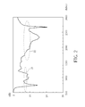
- FIG. 2 is a diagram illustrating the measured return loss of the mobile communication device and the antenna structure disposed therein according to a first embodiment of the present invention.
- the metal path from the first open end 1 5 which is short-circuited to the protruded ground 102 through the short-circuiting strip 142 is excited by the first coupling gap 17, such that a quarter-wavelength resonant mode can be excited at the lower frequency (such as near 750 MHz) and a higher-order resonant mode can be excited at the higher frequencies (such as near 2700 MHz).
- the metal path from the second open end 16 which is short-circuited to the protruded ground 102 through the short-circuiting strip 142, is excited by the second coupling gap 18, such that a quarter-wavelength resonant mode can be excited at the lower frequencies (such as, 1000 MHz nearby).
- these two lower-frequency resonant modes can be combined to form a wide first (lower-frequency) operating band (such as, the first operating band 21 shown in FIG. 2 ) at least covering from about 704 MHz to 960 MHz.
- each of them is able to form a quarter-wavelength resonant mode at the higher frequencies (such as, 1950 MHz and 2300 MHz nearby), respectively.
- these two higher-frequency resonant modes can be combined with the higher-order resonant mode (such as near 2700 MHz) excited by the first coupling gap 17 by exciting the metal path from the first open end 1 5 which is short-circuited to the protruded ground 102 through the short-circuiting strip 142 in order to form a wide second (higher-frequency) operating band (such as, the first operating band 22 shown in FIG.
- the first operating band 21 may cover the three-band LTE700/GSM850/900 operation
- the second operating band 22 may cover the five-band GSM1 800/1 900/UMTS/LTE2300/2500 operation, thereby the antenna structure can cover the eight-band LTE/WWAN operation. Therefore, the antenna structure of the mobile communication device can cover operating bands of all mobile communication systems at present.
- the antenna structure of the present invention also has a simple structure and is easy to manufacture, which can satisfy practical applications.
- the grounding element 10 of the antenna structure and the substrate 12 are located on different planes of three-dimensional space.
- the main ground 101 and the protruded ground 102 of the grounding element 10 are located on a first plane (such as, the XY plane shown in FIG. 1 );
- the substrate 12 comprises a first partial section 121 and a second partial section 1 22 forming an L shape, the first partial section 121 of the substrate 1 2 having the short-circuiting strip 142 is located on a second plane (such as, the XZ plane shown in FIG. 1 ) perpendicular to the first plane, and the second partial section 122 of the substrate 12 having the antenna element 11 is located on a third plane (such as, another XY plane shown in FIG. 1 ) parallel to the first plane.
- FIG. 2 is a diagram illustrating the measured return loss of the mobile communication device and the antenna structure disposed therein according to a first embodiment of the present invention.
- the size of the mobile communication device 1 is as follows: the main ground 101 has a length of 105 mm and a width of 55 mm; the protruded ground 102 has a length of 10 mm and a width of 10 mm; the second partial section 122 of the substrate 12 which is parallel to the protruded ground 102 has a length of 55 mm, a width of 10 mm, and a thickness of 0.8 mm; the first partial section 121 of the substrate 12 which is perpendicular to the protruded ground 102 has a length of 55 mm, a width of 8 mm, and a thickness of 0.8 mm.
- the first operating band 21 may cover the three-band LTE700/GSM850/900 operation (from about 704 MHz to 960 MHz), and the second operating band 22 may cover the five-band GSM1800/1900/UMTS/LTE2300/2500 operation (from about 1710 MHz to 2690 MHz), thereby the antenna structure can satisfy requirements of the eight-band LTE/WWAN operation.
- the size of the protruded ground 102 is capable of configuring with a USB connector, such that the integration of the antenna and other electronic elements functioning as a data transmission port of the mobile communication device can be achieved.
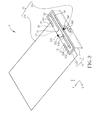
- FIG. 3 is a diagram illustrating a mobile communication device 3 and an antenna structure disposed therein according to a second embodiment of the present invention.
- the structure of the mobile communication device 3 shown in the second embodiment is similar to that of the mobile communication device 1 shown in the first embodiment, and the difference between them is that a radiating portion 34 of the antenna structure of the mobile communication device 3 shown in FIG.
- the shorting point 341 is electrically connected to the protruded ground 102 through a short-circuiting strip 342, wherein the short-circuiting strip 342 includes at least two bends, and a length of the short-circuiting strip 342 is at least 1.5 times that of a distance between the shorting point 341 and the protruded ground 102.
- the short-circuiting strip 342 By bending the short-circuiting strip 342, the length of the short-circuiting strip 342 can be extended in order to adjust the resonant modes of the antenna element 11 and reduce the overall size of the antenna.
- the structure of the mobile communication device 3 of the second embodiment is similar to that of the mobile communication device 1 of the first embodiment, and forms two similar wide operating bands covering the eight-band LTE/WWAN operation.
- FIG. 4 is a diagram illustrating a mobile communication device and an antenna structure disposed therein according to a third embodiment of the present invention.
- the structure of the mobile communication device 4 shown in the third embodiment is similar to that of the mobile communication device 1 shown in the first embodiment, and the difference between them is that an electronic element 49 functioning as a data transmission port can be disposed on the second surface of the protruded ground 102 of the mobile communication device 4 shown in FIG. 4 , which is opposite to the first surface of the protruded ground 102 used for accommodating the antenna element 11, such that the electronic element 49 can provide a signal transmission interface for communicating the mobile communication device 4 with an external equipment.
- the abovementioned electronic element 49 can be implemented by a USB connector, but this in no way should be considered as a limitation of the present invention.
- the architecture of the mobile communication device 43 of the third embodiment is similar to that of the mobile communication device 1 of the first embodiment, and forms two similar wide operating bands covering the eight-band LTE/WWAN operation.
- the number of the bends of the radiating portion and/or the short-circuiting strip is not limited, and the bending direction, the bending angle, and the bending shape of the bends should not be considered as a limitation of the present invention.
- a mobile communication device and its antenna structure which include an antenna capable of forming two wide operating bands.
- Such antenna has a simple structure as well as a protruded ground suitable for integrating with electronic elements functioning as a data transmission port.
- the two operating bands of the antenna may cover the three-band LTE700/GSM850/900 operation (from about 704 MHz to 960 MHz) and the five-band GSM1 800/1 900/UMTS/LTE2300/2500 operation (from about 1 71 0 MHz to 2690 MHz), respectively, thereby covering operating bands of all mobile communication systems at present.
Landscapes
- Engineering & Computer Science (AREA)
- Computer Networks & Wireless Communication (AREA)
- Support Of Aerials (AREA)
- Details Of Aerials (AREA)
- Telephone Set Structure (AREA)
- Waveguide Aerials (AREA)
Abstract
Description
- The present invention relates to mobile communication device comprising an antenna structure according to the pre-characterizing clauses of claim 1.
- Mobile communication devices are required to be light and small, such that small size, multi-band operations, as well as the integration of an internal antenna and other electronic elements on the system circuit board of the device becomes an essential design consideration. However, in order to obtain wideband operation and perform the integration of an internal antenna and other electronic elements on the system circuit board of the device, conventional antennas in mobile communication devices are directly disposed in the no-ground section of the system circuit board of the device, such that coupling effects between the antenna and the grounding plane can be reduced and sufficient operating bandwidth can be provided to cover the wideband WWAN operation. However, such WWAN antenna is mostly disposed on a single no-ground section of the system circuit board, which may reduce the design freedom of the internal electronic elements of the mobile communication device.
- In the prior art, such as
U.S. Patent No. 7,768,466 B2 with the invention entitled "Multiband folded loop antenna", a mobile antenna occupying three-dimensional space is disclosed, whose antenna is disposed on a single no-ground section to achieve wideband operation. However, by adopting such antenna configuration, the integration of the antenna and other electronic elements functioning as a data transmission port (inter alia a USB connector) of the mobile communication device cannot be achieved, which results in an inefficient configuration of the internal space of the mobile communication device. In addition, its operating band cannot cover the eight-band LTE/WWAN operation, including LTE700/GSM850/900/1800/1900/UMTS/LTE2300/2500, which cannot satisfy requirements of covering operating bands of all mobile communication systems at present. - Hence, how to provide a mobile communication device with two wide operating bands at least covering from about 704 MHz to 960 MHz and from about 1 710 MHz to 2690 MHz to satisfy the eight-band LTE/WWAN operation and perform the integration of an internal antenna and other electronic elements on the system circuit board of the device has become an important topic in this field.
- This in mind, the present invention aims at providing a mobile communication device comprising an antenna structure to solve the abovementioned problems of integration of a built-in antenna with electronic elements functioning as a data transmission port, such that a goal of covering multi-band operation can be achieved.
- This is achieved by a mobile communication device comprising an antenna structure according to claim 1. The dependent claims pertain to corresponding further developments and improvements.
- As will be seen more clearly from the detailed description following below, the claimed mobile communication device comprising an antenna structure is provided. The antenna structure may include a grounding element and an antenna element. The grounding element may include a main ground and a protruded ground, wherein the protruded ground is electrically connected to an edge of the main ground. The antenna element is disposed on the substrate. The antenna element may include a feeding portion and a radiating portion. The feeding portion may include a feeding point, a first strip and a second strip. The feeding point is electrically connected to a signal source being disposed on the grounding element. The first strip and the second strip are both connected to the feeding point, and open ends of the first strip and the second strip are extended toward opposite directions. In addition, a projection which is generated by projecting the feeding portion onto a plane where the grounding element is located, and the projection comprises a partial section of the protruded ground. The radiating portion may include a shorting point, a first open end and a second open end. The shorting point is electrically connected to the protruded ground by a short-circuiting strip. There is a first coupling gap between the first strip and a first section of the radiating portion having the first open end, and there is a second coupling gap between the second strip and a second section of the radiating portion having the second open end.
- The present invention includes the following advantages. By using the first coupling gap between the first section of the radiating portion having the first open end and the first strip of the feeding portion, a quarter-wavelength resonant mode can be excited at the lower frequency (such as near 750 MHz) and a higher-order resonant mode can be excited at the higher frequencies (such as near 2700 MHz). In addition, by using the second coupling gap between the second section of the radiating portion having the second open end and the second strip of the feeding portion, a quarter-wavelength resonant mode can be excited at the lower frequencies (such as near 1000 MHz), and then these two lower-frequency resonant modes can be combined to form a wide first (lower-frequency) operating band at least covering from about 704 MHz to 960 MHz. Moreover, since a length of the first strip of the feeding portion is different from a length of the second strip of the feeding portion, each of them is able to form a quarter-wavelength resonant mode at the higher frequencies (such as near 1 950 MHz and 2300 MHz), respectively. Then, these two higher-frequency resonant modes can be combined with the higher-order resonant mode (such as near 2700 MHz) excited by the first coupling gap in order to form a wide second (higher-frequency) operating band at least covering from about 1 710 MHz to 2690 MHz.
- In the following, the invention is further illustrated by way of example, taking reference to the accompanying drawings. Thereof
-
FIG. 1 is a diagram illustrating a mobile communication device and an antenna structure disposed therein according to a first embodiment of the present invention; -
FIG. 2 is a diagram illustrating the measured return loss of the mobile communication device and the antenna structure disposed therein according to a first embodiment of the present invention; -
FIG. 3 is a diagram illustrating a mobile communication device and an antenna structure disposed therein according to a second embodiment of the present invention; and -
FIG. 4 is a diagram illustrating a mobile communication device and an antenna structure disposed therein according to a third embodiment of the present invention. - The following description is of the best-contemplated mode of carrying out the present invention. A detailed description is given in the following embodiments with reference to the accompanying drawings.
- Certain terms are used throughout the description and following claims to refer to particular components. As one skilled in the art will appreciate, manufacturers may refer to a component by different names. This document does not intend to distinguish between components that differ in name but not function. In the following description and in the claims, the terms "include" and "comprise" are used in an open-ended fashion, and thus should be interpreted to mean "include, but not limited to ...". Also, the term "couple" is intended to mean either an indirect or direct electrical connection. Accordingly, if one device is coupled to another device, that connection may be through a direct electrical connection, or through an indirect electrical connection via other devices and connections.
-
FIG. 1 is a diagram illustrating a mobile communication device and an antenna structure disposed therein according to a first embodiment of the present invention. In this embodiment, the mobile communication device 1 may include an antenna structure, wherein the antenna structure may include agrounding element 10 and anantenna element 11. Theground element 10 may include amain ground 101 and aprotruded ground 102, wherein theprotruded ground 102 is electrically connected to an edge of themain ground 101. - Furthermore, the
antenna element 11 is disposed on asubstrate 12. Theantenna element 11 may include a feeding portion 1 3 and aradiating portion 14. The feeding portion 1 3 may include afeeding point 131, a first strip 1 34 and a second strip 1 35. Thefeeding point 131 is electrically connected to asignal source 133 being disposed on thegrounding element 10 through a metal wire 1 32. The first strip 1 34 and thesecond strip 135 are both connected to thefeeding point 131, and open ends of the first strip 1 34 and the second strip 1 35 are extended toward opposite directions. A length of the first strip 1 34 from its open end to thefeeding point 131 is larger than 0.2 wavelength of the highest operating frequency of the second operating band; and/or a length of thesecond strip 135 from its open end to thefeeding point 131 is larger than 0.2 wavelength of the highest operating frequency of the second operating band. In addition, a projection is generated by projecting the feeding portion 1 3 onto a plane where thegrounding element 10 is located, and the projection comprises a partial section of theprotruded ground 102. The radiatingportion 14 may include ashorting point 141 , a first open end 1 5 and a secondopen end 16. Theshorting point 141 is electrically connected to theprotruded ground 102 by a short-circuiting strip 142. Be noted that there is a first coupling gap 1 7 between afirst section 151 of theradiating portion 14 having the first open end 1 5 and the first strip 1 34, and there is asecond coupling gap 18 between asecond section 161 of theradiating portion 14 having the second open end 1 6 and the second strip 1 35. Herein thefirst coupling gap 17 is smaller than 2 mm, and thesecond coupling gap 18 is smaller than 2 mm. - Please refer to
FIG. 1 together withFIG. 2. FIG. 2 is a diagram illustrating the measured return loss of the mobile communication device and the antenna structure disposed therein according to a first embodiment of the present invention. In this embodiment, by using the first strip 1 34 of thefeeding portion 13, the metal path from the first open end 1 5 which is short-circuited to theprotruded ground 102 through the short-circuiting strip 142 is excited by thefirst coupling gap 17, such that a quarter-wavelength resonant mode can be excited at the lower frequency (such as near 750 MHz) and a higher-order resonant mode can be excited at the higher frequencies (such as near 2700 MHz). In addition, by using thesecond strip 135 of the feedingportion 13, the metal path from the secondopen end 16 which is short-circuited to theprotruded ground 102 through the short-circuiting strip 142, is excited by thesecond coupling gap 18, such that a quarter-wavelength resonant mode can be excited at the lower frequencies (such as, 1000 MHz nearby). Then, these two lower-frequency resonant modes can be combined to form a wide first (lower-frequency) operating band (such as, thefirst operating band 21 shown inFIG. 2 ) at least covering from about 704 MHz to 960 MHz. Moreover, since a length of the first strip 1 34 of the feeding portion 1 3 is different from a length of thesecond strip 135 of the feedingportion 13, each of them is able to form a quarter-wavelength resonant mode at the higher frequencies (such as, 1950 MHz and 2300 MHz nearby), respectively. Then, these two higher-frequency resonant modes can be combined with the higher-order resonant mode (such as near 2700 MHz) excited by thefirst coupling gap 17 by exciting the metal path from the first open end 1 5 which is short-circuited to theprotruded ground 102 through the short-circuiting strip 142 in order to form a wide second (higher-frequency) operating band (such as, thefirst operating band 22 shown inFIG. 2 ) at least covering from about 1 710 MHz to 2690 MHz. Thefirst operating band 21 may cover the three-band LTE700/GSM850/900 operation, and thesecond operating band 22 may cover the five-band GSM1 800/1 900/UMTS/LTE2300/2500 operation, thereby the antenna structure can cover the eight-band LTE/WWAN operation. Therefore, the antenna structure of the mobile communication device can cover operating bands of all mobile communication systems at present. The antenna structure of the present invention also has a simple structure and is easy to manufacture, which can satisfy practical applications. - In this embodiment, the
grounding element 10 of the antenna structure and thesubstrate 12 are located on different planes of three-dimensional space. For example, themain ground 101 and theprotruded ground 102 of thegrounding element 10 are located on a first plane (such as, the XY plane shown inFIG. 1 ); thesubstrate 12 comprises a firstpartial section 121 and a second partial section 1 22 forming an L shape, the firstpartial section 121 of the substrate 1 2 having the short-circuiting strip 142 is located on a second plane (such as, the XZ plane shown inFIG. 1 ) perpendicular to the first plane, and the secondpartial section 122 of thesubstrate 12 having theantenna element 11 is located on a third plane (such as, another XY plane shown inFIG. 1 ) parallel to the first plane. -
FIG. 2 is a diagram illustrating the measured return loss of the mobile communication device and the antenna structure disposed therein according to a first embodiment of the present invention. In this embodiment, the size of the mobile communication device 1 is as follows: themain ground 101 has a length of 105 mm and a width of 55 mm; theprotruded ground 102 has a length of 10 mm and a width of 10 mm; the secondpartial section 122 of thesubstrate 12 which is parallel to theprotruded ground 102 has a length of 55 mm, a width of 10 mm, and a thickness of 0.8 mm; the firstpartial section 121 of thesubstrate 12 which is perpendicular to theprotruded ground 102 has a length of 55 mm, a width of 8 mm, and a thickness of 0.8 mm. According to the experimental results and a 6-dB return-loss definition, thefirst operating band 21 may cover the three-band LTE700/GSM850/900 operation (from about 704 MHz to 960 MHz), and thesecond operating band 22 may cover the five-band GSM1800/1900/UMTS/LTE2300/2500 operation (from about 1710 MHz to 2690 MHz), thereby the antenna structure can satisfy requirements of the eight-band LTE/WWAN operation. The size of theprotruded ground 102 is capable of configuring with a USB connector, such that the integration of the antenna and other electronic elements functioning as a data transmission port of the mobile communication device can be achieved. - Please refer to
FIG. 3. FIG. 3 is a diagram illustrating amobile communication device 3 and an antenna structure disposed therein according to a second embodiment of the present invention. The structure of themobile communication device 3 shown in the second embodiment is similar to that of the mobile communication device 1 shown in the first embodiment, and the difference between them is that a radiatingportion 34 of the antenna structure of themobile communication device 3 shown inFIG. 3 has ashorting point 341, and theshorting point 341 is electrically connected to theprotruded ground 102 through a short-circuiting strip 342, wherein the short-circuiting strip 342 includes at least two bends, and a length of the short-circuiting strip 342 is at least 1.5 times that of a distance between theshorting point 341 and theprotruded ground 102. By bending the short-circuiting strip 342, the length of the short-circuiting strip 342 can be extended in order to adjust the resonant modes of theantenna element 11 and reduce the overall size of the antenna. Moreover, the structure of themobile communication device 3 of the second embodiment is similar to that of the mobile communication device 1 of the first embodiment, and forms two similar wide operating bands covering the eight-band LTE/WWAN operation. - Please refer to
FIG. 4. FIG. 4 is a diagram illustrating a mobile communication device and an antenna structure disposed therein according to a third embodiment of the present invention. The structure of the mobile communication device 4 shown in the third embodiment is similar to that of the mobile communication device 1 shown in the first embodiment, and the difference between them is that anelectronic element 49 functioning as a data transmission port can be disposed on the second surface of theprotruded ground 102 of the mobile communication device 4 shown inFIG. 4 , which is opposite to the first surface of theprotruded ground 102 used for accommodating theantenna element 11, such that theelectronic element 49 can provide a signal transmission interface for communicating the mobile communication device 4 with an external equipment. The abovementionedelectronic element 49 can be implemented by a USB connector, but this in no way should be considered as a limitation of the present invention. Moreover, the architecture of the mobile communication device 43 of the third embodiment is similar to that of the mobile communication device 1 of the first embodiment, and forms two similar wide operating bands covering the eight-band LTE/WWAN operation. - The number of the bends of the radiating portion and/or the short-circuiting strip is not limited, and the bending direction, the bending angle, and the bending shape of the bends should not be considered as a limitation of the present invention.
- In summary, a mobile communication device and its antenna structure are provided, which include an antenna capable of forming two wide operating bands. Such antenna has a simple structure as well as a protruded ground suitable for integrating with electronic elements functioning as a data transmission port. Besides, the two operating bands of the antenna may cover the three-band LTE700/GSM850/900 operation (from about 704 MHz to 960 MHz) and the five-band GSM1 800/1 900/UMTS/LTE2300/2500 operation (from about 1 71 0 MHz to 2690 MHz), respectively, thereby covering operating bands of all mobile communication systems at present.
- All combinations and sub-combinations of above-described features also belong to the invention.
Claims (8)
- A mobile communication device (1) comprising an antenna structure, the antenna structure characterized by:a grounding element (10), comprising a main ground (101) and a protruded ground (102), wherein the protruded ground (102) is electrically connected to an edge of the main ground (101); andan antenna element (11), disposed on a substrate (12), the antenna element (11) comprising:a feeding portion (13), comprising:a feeding point (131), electrically connected to a signal source (133) being disposed on the grounding element (10); anda first strip (134) and a second strip (135), wherein the first strip (134) and the second strip (135) are both connected to the feeding point (131), open ends of the first strip (134) and the second strip (135) are extended toward opposite directions, a projection is generated by projecting the feeding portion (13) onto a plane where the grounding element (10) is located, and the projection comprises a partial section of the protruded ground (102); anda radiating portion (14), comprising:a shorting point (141), electrically connected to the protruded ground (102) by a short-circuiting strip (142) ; anda first open end (15) and a second open end (16);wherein there is a first coupling gap (17) between the first strip (134) and a first section (151) of the radiating portion (14) having the first open end (15), and there is a second coupling gap (18) between the second strip (135) and a second section (161) of the radiating portion (14) having the second open end (16).
- The mobile communication device (4) according to claim 1, further characterized in that the protruded ground (102) is used for accommodating an electronic element (49) functioning as a data transmission port of the mobile communication device (4) .
- The mobile communication device (3) according to claim 1, further characterized in that the short-circuiting strip (342) comprises at least two bends, and a length of the short-circuiting strip (342) is at least 1.5 times that of a distance between the shorting point (341) and the protruded ground (102).
- The mobile communication device (1, 3, 4) according to claim 1, further characterized in that a length of the first strip (134) from its open end to the feeding point (131) is larger than 0.2 wavelength of the highest operating frequency of the second operating band.
- The mobile communication device (1, 3, 4) according to claim 1, further characterized in that a length of the second strip (135) from its open end to the feeding point (131) is larger than 0.2 wavelength of the highest operating frequency of the second operating band.
- The mobile communication device (1, 3, 4) according to claim 1, further characterized in that a length of the first strip (134) is different from a length of the second strip (135).
- The mobile communication device (1) according to claim 1, further characterized in that the first coupling gap (17) is smaller than 2 mm, and the second coupling gap (18) is smaller than 2 mm.
- The mobile communication device (1) according to claim 1, further characterized in that the main ground (101) and the protruded ground (102) are located on a first plane, the substrate (12) comprises a first partial section (121) and a second partial section (122) forming an L shape, the first partial section (121) of the substrate (12) having the short-circuiting strip (142) is located on a second plane perpendicular to the first plane, and the second partial section (122) of the substrate (12) having the antenna element (11) is located on a third plane parallel to the first plane.
Applications Claiming Priority (1)
| Application Number | Priority Date | Filing Date | Title |
|---|---|---|---|
| TW100106391A TWI450441B (en) | 2011-02-25 | 2011-02-25 | Mobile communication device and antenna structure thereof |
Publications (2)
| Publication Number | Publication Date |
|---|---|
| EP2493015A1 true EP2493015A1 (en) | 2012-08-29 |
| EP2493015B1 EP2493015B1 (en) | 2016-06-29 |
Family
ID=45715283
Family Applications (1)
| Application Number | Title | Priority Date | Filing Date |
|---|---|---|---|
| EP11167067.5A Active EP2493015B1 (en) | 2011-02-25 | 2011-05-23 | Mobile communication device and antenna structure thereof |
Country Status (6)
| Country | Link |
|---|---|
| US (1) | US8684272B2 (en) |
| EP (1) | EP2493015B1 (en) |
| JP (1) | JP5323886B2 (en) |
| KR (1) | KR101231016B1 (en) |
| AU (1) | AU2012200663A1 (en) |
| TW (1) | TWI450441B (en) |
Cited By (5)
| Publication number | Priority date | Publication date | Assignee | Title |
|---|---|---|---|---|
| CN103403962A (en) * | 2012-10-17 | 2013-11-20 | 华为终端有限公司 | Multimode broadband antenna module and wireless terminal |
| CN103682586A (en) * | 2012-09-26 | 2014-03-26 | 深圳富泰宏精密工业有限公司 | Antenna structure |
| CN104124524A (en) * | 2013-04-26 | 2014-10-29 | 深圳富泰宏精密工业有限公司 | Antenna structure and wireless communication device provided with same |
| CN108449897A (en) * | 2018-03-19 | 2018-08-24 | 广东欧珀移动通信有限公司 | Housing, antenna assembly and electronic equipment |
| CN115347371A (en) * | 2021-05-12 | 2022-11-15 | Oppo广东移动通信有限公司 | Antenna assembly and electronic equipment |
Families Citing this family (20)
| Publication number | Priority date | Publication date | Assignee | Title |
|---|---|---|---|---|
| US9276317B1 (en) * | 2012-03-02 | 2016-03-01 | Amazon Technologies, Inc. | Quad-mode antenna |
| TWI508367B (en) * | 2012-09-27 | 2015-11-11 | Ind Tech Res Inst | Communication device and method for designing antenna element thereof |
| FR3003697B1 (en) * | 2013-03-20 | 2015-04-10 | Aviwest | BROADBAND MULTI-ANTENNA SYSTEM CONSISTING OF AT LEAST TWO ANTENNAS OF THE SAME SHAPE AND SAME DIMENSION. |
| CN104134869B (en) * | 2013-04-30 | 2019-11-01 | 深圳富泰宏精密工业有限公司 | Antenna structure and wireless communication device with the antenna structure |
| KR102036046B1 (en) * | 2013-05-29 | 2019-10-24 | 삼성전자 주식회사 | Antenna device and electric device having the same |
| US10044110B2 (en) * | 2013-07-01 | 2018-08-07 | Qualcomm Incorporated | Antennas with shared grounding structure |
| TWI530019B (en) * | 2013-08-30 | 2016-04-11 | 華碩電腦股份有限公司 | Electronic device |
| CN104577338B (en) * | 2013-10-09 | 2019-06-18 | 深圳富泰宏精密工业有限公司 | Antenna module and wireless communication device with the antenna module |
| CN104681928A (en) * | 2013-11-30 | 2015-06-03 | 深圳富泰宏精密工业有限公司 | Multi-frequency antenna structure |
| KR102162810B1 (en) * | 2014-03-14 | 2020-10-07 | 삼성전자주식회사 | Method of Providing Antenna by Using Component Included in Device |
| CN104241822B (en) * | 2014-09-12 | 2017-02-22 | 昆山联滔电子有限公司 | Planar antenna |
| TWI590524B (en) * | 2014-10-15 | 2017-07-01 | 宏碁股份有限公司 | Antenna system |
| TWI594498B (en) * | 2015-03-16 | 2017-08-01 | 南臺科技大學 | Multi-frequency monopole antenna for tablet and botebook computers |
| US20170149136A1 (en) * | 2015-11-20 | 2017-05-25 | Taoglas Limited | Eight-frequency band antenna |
| CN106816706B (en) * | 2015-11-30 | 2020-07-14 | 深圳富泰宏精密工业有限公司 | Antenna structure and wireless communication device using the same |
| TWI593167B (en) * | 2015-12-08 | 2017-07-21 | 財團法人工業技術研究院 | Antenna array |
| WO2019017322A1 (en) * | 2017-07-20 | 2019-01-24 | パナソニックIpマネジメント株式会社 | Multiband compatible antenna and wireless communication device |
| TWI679809B (en) * | 2018-10-18 | 2019-12-11 | 啓碁科技股份有限公司 | Antenna structure and electronic device |
| CN109980341B (en) * | 2019-03-05 | 2020-12-25 | 惠州Tcl移动通信有限公司 | Antenna and intelligent terminal |
| TWI845052B (en) * | 2022-12-07 | 2024-06-11 | 廣達電腦股份有限公司 | Antenna structure |
Citations (3)
| Publication number | Priority date | Publication date | Assignee | Title |
|---|---|---|---|---|
| EP1439604A1 (en) * | 2003-01-15 | 2004-07-21 | Filtronic LK Oy | Multiband antenna |
| US20070008228A1 (en) * | 2005-07-11 | 2007-01-11 | Kabushiki Kaisha Toshiba | Antenna device, mobile terminal and RFID tag |
| US7768466B2 (en) | 2008-04-09 | 2010-08-03 | Acer Incorporated | Multiband folded loop antenna |
Family Cites Families (13)
| Publication number | Priority date | Publication date | Assignee | Title |
|---|---|---|---|---|
| JPH0738325A (en) | 1993-07-19 | 1995-02-07 | Hitachi Cable Ltd | Wideband dipole antenna |
| JP4346964B2 (en) | 2003-06-09 | 2009-10-21 | 峰光電子株式会社 | Multifrequency T-shaped antenna |
| KR100619695B1 (en) | 2004-06-23 | 2006-09-08 | 엘지전자 주식회사 | Antenna and portable terminal with same |
| JP2006319629A (en) | 2005-05-12 | 2006-11-24 | Tyco Electronics Amp Kk | Flat antenna |
| JP2006319767A (en) | 2005-05-13 | 2006-11-24 | Sony Corp | Planar antenna |
| JP4558598B2 (en) | 2005-07-14 | 2010-10-06 | 日本アンテナ株式会社 | Planar antenna |
| JP4645603B2 (en) | 2007-02-22 | 2011-03-09 | 株式会社村田製作所 | Antenna structure and wireless communication apparatus including the same |
| JP5032962B2 (en) | 2007-11-30 | 2012-09-26 | 富士通コンポーネント株式会社 | Antenna device |
| JP4871949B2 (en) | 2007-12-20 | 2012-02-08 | 原田工業株式会社 | Patch antenna device |
| TWI343675B (en) * | 2008-03-06 | 2011-06-11 | Univ Nat Sun Yat Sen | A multiband antenna |
| KR100980218B1 (en) | 2008-03-31 | 2010-09-06 | 주식회사 에이스테크놀로지 | Internal Antenna Providing Impedance Maching for Multi Band |
| TWI360914B (en) * | 2008-05-23 | 2012-03-21 | Univ Nat Sun Yat Sen | A mobile communication device antenna |
| JP2011010017A (en) | 2009-06-25 | 2011-01-13 | Midori Anzen Co Ltd | Dipole antenna unit and its module |
-
2011
- 2011-02-25 TW TW100106391A patent/TWI450441B/en active
- 2011-04-20 US US13/091,096 patent/US8684272B2/en active Active
- 2011-05-04 KR KR1020110042443A patent/KR101231016B1/en not_active Expired - Fee Related
- 2011-05-12 JP JP2011107377A patent/JP5323886B2/en not_active Expired - Fee Related
- 2011-05-23 EP EP11167067.5A patent/EP2493015B1/en active Active
-
2012
- 2012-02-06 AU AU2012200663A patent/AU2012200663A1/en not_active Abandoned
Patent Citations (3)
| Publication number | Priority date | Publication date | Assignee | Title |
|---|---|---|---|---|
| EP1439604A1 (en) * | 2003-01-15 | 2004-07-21 | Filtronic LK Oy | Multiband antenna |
| US20070008228A1 (en) * | 2005-07-11 | 2007-01-11 | Kabushiki Kaisha Toshiba | Antenna device, mobile terminal and RFID tag |
| US7768466B2 (en) | 2008-04-09 | 2010-08-03 | Acer Incorporated | Multiband folded loop antenna |
Cited By (7)
| Publication number | Priority date | Publication date | Assignee | Title |
|---|---|---|---|---|
| CN103682586A (en) * | 2012-09-26 | 2014-03-26 | 深圳富泰宏精密工业有限公司 | Antenna structure |
| CN103682586B (en) * | 2012-09-26 | 2018-06-19 | 深圳富泰宏精密工业有限公司 | Antenna structure |
| CN103403962A (en) * | 2012-10-17 | 2013-11-20 | 华为终端有限公司 | Multimode broadband antenna module and wireless terminal |
| US9300041B2 (en) | 2012-10-17 | 2016-03-29 | Huawei Device Co., Ltd. | Multimode broadband antenna module and wireless terminal |
| CN104124524A (en) * | 2013-04-26 | 2014-10-29 | 深圳富泰宏精密工业有限公司 | Antenna structure and wireless communication device provided with same |
| CN108449897A (en) * | 2018-03-19 | 2018-08-24 | 广东欧珀移动通信有限公司 | Housing, antenna assembly and electronic equipment |
| CN115347371A (en) * | 2021-05-12 | 2022-11-15 | Oppo广东移动通信有限公司 | Antenna assembly and electronic equipment |
Also Published As
| Publication number | Publication date |
|---|---|
| US8684272B2 (en) | 2014-04-01 |
| KR20120098367A (en) | 2012-09-05 |
| EP2493015B1 (en) | 2016-06-29 |
| TW201236272A (en) | 2012-09-01 |
| JP2012178810A (en) | 2012-09-13 |
| JP5323886B2 (en) | 2013-10-23 |
| US20120218163A1 (en) | 2012-08-30 |
| AU2012200663A1 (en) | 2012-09-13 |
| TWI450441B (en) | 2014-08-21 |
| KR101231016B1 (en) | 2013-02-07 |
Similar Documents
| Publication | Publication Date | Title |
|---|---|---|
| EP2493015B1 (en) | Mobile communication device and antenna structure thereof | |
| EP2493011A1 (en) | Mobile communication device and antenna structure therein | |
| CN104795623B (en) | Mobile device and manufacturing method thereof | |
| EP2555320B1 (en) | Communication electronic device and antenna structure therein | |
| US9325059B2 (en) | Communication device and antenna structure thereof | |
| EP2509158B1 (en) | Communication electronic device and antenna structure thereof | |
| EP2445053A1 (en) | Mobile communication device and antenna | |
| TWI619314B (en) | Multiple frequency antenna | |
| EP2610967B1 (en) | Communication device and antenna structure therein | |
| EP2511978A1 (en) | Mobile communication device and antenna structure therein | |
| CN113078449A (en) | Antenna structure and wireless communication device with same | |
| US8947314B2 (en) | Mobile communication device and built-in antenna integrated with a ground portion thereof | |
| US11329382B1 (en) | Antenna structure | |
| CN112397888A (en) | mobile device | |
| CN102683829B (en) | Mobile communication device and antenna structure thereof | |
| EP2662925A1 (en) | Communication device and antenna structure therein | |
| US9306274B2 (en) | Antenna device and antenna mounting method | |
| CN113078444A (en) | Antenna structure and wireless communication device with same | |
| US20140357203A1 (en) | Antenna structure and wireless communication device using the same | |
| US20140210673A1 (en) | Dual-band antenna of wireless communication apparatus | |
| CN113078445A (en) | Antenna structure and wireless communication device with same | |
| US9748633B2 (en) | Antenna structure |
Legal Events
| Date | Code | Title | Description |
|---|---|---|---|
| PUAI | Public reference made under article 153(3) epc to a published international application that has entered the european phase |
Free format text: ORIGINAL CODE: 0009012 |
|
| AK | Designated contracting states |
Kind code of ref document: A1 Designated state(s): AL AT BE BG CH CY CZ DE DK EE ES FI FR GB GR HR HU IE IS IT LI LT LU LV MC MK MT NL NO PL PT RO RS SE SI SK SM TR |
|
| AX | Request for extension of the european patent |
Extension state: BA ME |
|
| 17P | Request for examination filed |
Effective date: 20130227 |
|
| 17Q | First examination report despatched |
Effective date: 20130515 |
|
| GRAP | Despatch of communication of intention to grant a patent |
Free format text: ORIGINAL CODE: EPIDOSNIGR1 |
|
| INTG | Intention to grant announced |
Effective date: 20160203 |
|
| GRAS | Grant fee paid |
Free format text: ORIGINAL CODE: EPIDOSNIGR3 |
|
| GRAA | (expected) grant |
Free format text: ORIGINAL CODE: 0009210 |
|
| AK | Designated contracting states |
Kind code of ref document: B1 Designated state(s): AL AT BE BG CH CY CZ DE DK EE ES FI FR GB GR HR HU IE IS IT LI LT LU LV MC MK MT NL NO PL PT RO RS SE SI SK SM TR |
|
| REG | Reference to a national code |
Ref country code: GB Ref legal event code: FG4D |
|
| REG | Reference to a national code |
Ref country code: CH Ref legal event code: EP |
|
| REG | Reference to a national code |
Ref country code: AT Ref legal event code: REF Ref document number: 809751 Country of ref document: AT Kind code of ref document: T Effective date: 20160715 |
|
| REG | Reference to a national code |
Ref country code: IE Ref legal event code: FG4D |
|
| REG | Reference to a national code |
Ref country code: DE Ref legal event code: R096 Ref document number: 602011027694 Country of ref document: DE |
|
| REG | Reference to a national code |
Ref country code: LT Ref legal event code: MG4D |
|
| PG25 | Lapsed in a contracting state [announced via postgrant information from national office to epo] |
Ref country code: FI Free format text: LAPSE BECAUSE OF FAILURE TO SUBMIT A TRANSLATION OF THE DESCRIPTION OR TO PAY THE FEE WITHIN THE PRESCRIBED TIME-LIMIT Effective date: 20160629 Ref country code: LT Free format text: LAPSE BECAUSE OF FAILURE TO SUBMIT A TRANSLATION OF THE DESCRIPTION OR TO PAY THE FEE WITHIN THE PRESCRIBED TIME-LIMIT Effective date: 20160629 Ref country code: NO Free format text: LAPSE BECAUSE OF FAILURE TO SUBMIT A TRANSLATION OF THE DESCRIPTION OR TO PAY THE FEE WITHIN THE PRESCRIBED TIME-LIMIT Effective date: 20160929 |
|
| REG | Reference to a national code |
Ref country code: NL Ref legal event code: MP Effective date: 20160629 |
|
| PG25 | Lapsed in a contracting state [announced via postgrant information from national office to epo] |
Ref country code: HR Free format text: LAPSE BECAUSE OF FAILURE TO SUBMIT A TRANSLATION OF THE DESCRIPTION OR TO PAY THE FEE WITHIN THE PRESCRIBED TIME-LIMIT Effective date: 20160629 Ref country code: RS Free format text: LAPSE BECAUSE OF FAILURE TO SUBMIT A TRANSLATION OF THE DESCRIPTION OR TO PAY THE FEE WITHIN THE PRESCRIBED TIME-LIMIT Effective date: 20160629 Ref country code: SE Free format text: LAPSE BECAUSE OF FAILURE TO SUBMIT A TRANSLATION OF THE DESCRIPTION OR TO PAY THE FEE WITHIN THE PRESCRIBED TIME-LIMIT Effective date: 20160629 Ref country code: NL Free format text: LAPSE BECAUSE OF FAILURE TO SUBMIT A TRANSLATION OF THE DESCRIPTION OR TO PAY THE FEE WITHIN THE PRESCRIBED TIME-LIMIT Effective date: 20160629 Ref country code: LV Free format text: LAPSE BECAUSE OF FAILURE TO SUBMIT A TRANSLATION OF THE DESCRIPTION OR TO PAY THE FEE WITHIN THE PRESCRIBED TIME-LIMIT Effective date: 20160629 Ref country code: GR Free format text: LAPSE BECAUSE OF FAILURE TO SUBMIT A TRANSLATION OF THE DESCRIPTION OR TO PAY THE FEE WITHIN THE PRESCRIBED TIME-LIMIT Effective date: 20160930 |
|
| REG | Reference to a national code |
Ref country code: AT Ref legal event code: MK05 Ref document number: 809751 Country of ref document: AT Kind code of ref document: T Effective date: 20160629 |
|
| PG25 | Lapsed in a contracting state [announced via postgrant information from national office to epo] |
Ref country code: RO Free format text: LAPSE BECAUSE OF FAILURE TO SUBMIT A TRANSLATION OF THE DESCRIPTION OR TO PAY THE FEE WITHIN THE PRESCRIBED TIME-LIMIT Effective date: 20160629 Ref country code: EE Free format text: LAPSE BECAUSE OF FAILURE TO SUBMIT A TRANSLATION OF THE DESCRIPTION OR TO PAY THE FEE WITHIN THE PRESCRIBED TIME-LIMIT Effective date: 20160629 Ref country code: IT Free format text: LAPSE BECAUSE OF FAILURE TO SUBMIT A TRANSLATION OF THE DESCRIPTION OR TO PAY THE FEE WITHIN THE PRESCRIBED TIME-LIMIT Effective date: 20160629 Ref country code: IS Free format text: LAPSE BECAUSE OF FAILURE TO SUBMIT A TRANSLATION OF THE DESCRIPTION OR TO PAY THE FEE WITHIN THE PRESCRIBED TIME-LIMIT Effective date: 20161029 Ref country code: SK Free format text: LAPSE BECAUSE OF FAILURE TO SUBMIT A TRANSLATION OF THE DESCRIPTION OR TO PAY THE FEE WITHIN THE PRESCRIBED TIME-LIMIT Effective date: 20160629 Ref country code: CZ Free format text: LAPSE BECAUSE OF FAILURE TO SUBMIT A TRANSLATION OF THE DESCRIPTION OR TO PAY THE FEE WITHIN THE PRESCRIBED TIME-LIMIT Effective date: 20160629 |
|
| PG25 | Lapsed in a contracting state [announced via postgrant information from national office to epo] |
Ref country code: BE Free format text: LAPSE BECAUSE OF FAILURE TO SUBMIT A TRANSLATION OF THE DESCRIPTION OR TO PAY THE FEE WITHIN THE PRESCRIBED TIME-LIMIT Effective date: 20160629 Ref country code: AT Free format text: LAPSE BECAUSE OF FAILURE TO SUBMIT A TRANSLATION OF THE DESCRIPTION OR TO PAY THE FEE WITHIN THE PRESCRIBED TIME-LIMIT Effective date: 20160629 Ref country code: SM Free format text: LAPSE BECAUSE OF FAILURE TO SUBMIT A TRANSLATION OF THE DESCRIPTION OR TO PAY THE FEE WITHIN THE PRESCRIBED TIME-LIMIT Effective date: 20160629 Ref country code: PL Free format text: LAPSE BECAUSE OF FAILURE TO SUBMIT A TRANSLATION OF THE DESCRIPTION OR TO PAY THE FEE WITHIN THE PRESCRIBED TIME-LIMIT Effective date: 20160629 Ref country code: PT Free format text: LAPSE BECAUSE OF FAILURE TO SUBMIT A TRANSLATION OF THE DESCRIPTION OR TO PAY THE FEE WITHIN THE PRESCRIBED TIME-LIMIT Effective date: 20161031 Ref country code: ES Free format text: LAPSE BECAUSE OF FAILURE TO SUBMIT A TRANSLATION OF THE DESCRIPTION OR TO PAY THE FEE WITHIN THE PRESCRIBED TIME-LIMIT Effective date: 20160629 |
|
| REG | Reference to a national code |
Ref country code: DE Ref legal event code: R097 Ref document number: 602011027694 Country of ref document: DE |
|
| REG | Reference to a national code |
Ref country code: FR Ref legal event code: PLFP Year of fee payment: 7 |
|
| PLBE | No opposition filed within time limit |
Free format text: ORIGINAL CODE: 0009261 |
|
| STAA | Information on the status of an ep patent application or granted ep patent |
Free format text: STATUS: NO OPPOSITION FILED WITHIN TIME LIMIT |
|
| PG25 | Lapsed in a contracting state [announced via postgrant information from national office to epo] |
Ref country code: DK Free format text: LAPSE BECAUSE OF FAILURE TO SUBMIT A TRANSLATION OF THE DESCRIPTION OR TO PAY THE FEE WITHIN THE PRESCRIBED TIME-LIMIT Effective date: 20160629 |
|
| 26N | No opposition filed |
Effective date: 20170330 |
|
| PG25 | Lapsed in a contracting state [announced via postgrant information from national office to epo] |
Ref country code: SI Free format text: LAPSE BECAUSE OF FAILURE TO SUBMIT A TRANSLATION OF THE DESCRIPTION OR TO PAY THE FEE WITHIN THE PRESCRIBED TIME-LIMIT Effective date: 20160629 Ref country code: LU Free format text: LAPSE BECAUSE OF NON-PAYMENT OF DUE FEES Effective date: 20170531 Ref country code: BG Free format text: LAPSE BECAUSE OF FAILURE TO SUBMIT A TRANSLATION OF THE DESCRIPTION OR TO PAY THE FEE WITHIN THE PRESCRIBED TIME-LIMIT Effective date: 20160929 |
|
| REG | Reference to a national code |
Ref country code: CH Ref legal event code: PL |
|
| PG25 | Lapsed in a contracting state [announced via postgrant information from national office to epo] |
Ref country code: MC Free format text: LAPSE BECAUSE OF FAILURE TO SUBMIT A TRANSLATION OF THE DESCRIPTION OR TO PAY THE FEE WITHIN THE PRESCRIBED TIME-LIMIT Effective date: 20160629 |
|
| REG | Reference to a national code |
Ref country code: IE Ref legal event code: MM4A |
|
| PG25 | Lapsed in a contracting state [announced via postgrant information from national office to epo] |
Ref country code: CH Free format text: LAPSE BECAUSE OF NON-PAYMENT OF DUE FEES Effective date: 20170531 Ref country code: LI Free format text: LAPSE BECAUSE OF NON-PAYMENT OF DUE FEES Effective date: 20170531 |
|
| PG25 | Lapsed in a contracting state [announced via postgrant information from national office to epo] |
Ref country code: LU Free format text: LAPSE BECAUSE OF NON-PAYMENT OF DUE FEES Effective date: 20170523 |
|
| REG | Reference to a national code |
Ref country code: FR Ref legal event code: PLFP Year of fee payment: 8 |
|
| PG25 | Lapsed in a contracting state [announced via postgrant information from national office to epo] |
Ref country code: IE Free format text: LAPSE BECAUSE OF NON-PAYMENT OF DUE FEES Effective date: 20170523 |
|
| PG25 | Lapsed in a contracting state [announced via postgrant information from national office to epo] |
Ref country code: MT Free format text: LAPSE BECAUSE OF NON-PAYMENT OF DUE FEES Effective date: 20170523 |
|
| PG25 | Lapsed in a contracting state [announced via postgrant information from national office to epo] |
Ref country code: AL Free format text: LAPSE BECAUSE OF FAILURE TO SUBMIT A TRANSLATION OF THE DESCRIPTION OR TO PAY THE FEE WITHIN THE PRESCRIBED TIME-LIMIT Effective date: 20160629 |
|
| PG25 | Lapsed in a contracting state [announced via postgrant information from national office to epo] |
Ref country code: HU Free format text: LAPSE BECAUSE OF FAILURE TO SUBMIT A TRANSLATION OF THE DESCRIPTION OR TO PAY THE FEE WITHIN THE PRESCRIBED TIME-LIMIT; INVALID AB INITIO Effective date: 20110523 |
|
| PG25 | Lapsed in a contracting state [announced via postgrant information from national office to epo] |
Ref country code: CY Free format text: LAPSE BECAUSE OF NON-PAYMENT OF DUE FEES Effective date: 20160629 |
|
| PG25 | Lapsed in a contracting state [announced via postgrant information from national office to epo] |
Ref country code: MK Free format text: LAPSE BECAUSE OF FAILURE TO SUBMIT A TRANSLATION OF THE DESCRIPTION OR TO PAY THE FEE WITHIN THE PRESCRIBED TIME-LIMIT Effective date: 20160629 |
|
| REG | Reference to a national code |
Ref country code: DE Ref legal event code: R082 Ref document number: 602011027694 Country of ref document: DE Representative=s name: STRAUS, ALEXANDER, DIPL.-CHEM.UNIV. DR.PHIL., DE Ref country code: DE Ref legal event code: R082 Ref document number: 602011027694 Country of ref document: DE Representative=s name: 2K PATENT- UND RECHTSANWAELTE PARTNERSCHAFT MB, DE |
|
| PG25 | Lapsed in a contracting state [announced via postgrant information from national office to epo] |
Ref country code: TR Free format text: LAPSE BECAUSE OF FAILURE TO SUBMIT A TRANSLATION OF THE DESCRIPTION OR TO PAY THE FEE WITHIN THE PRESCRIBED TIME-LIMIT Effective date: 20160629 |
|
| REG | Reference to a national code |
Ref country code: FR Ref legal event code: PLFP Year of fee payment: 13 |
|
| REG | Reference to a national code |
Ref country code: DE Ref legal event code: R082 Ref document number: 602011027694 Country of ref document: DE Representative=s name: STRAUS, ALEXANDER, DIPL.-CHEM.UNIV. DR.PHIL., DE |
|
| PGFP | Annual fee paid to national office [announced via postgrant information from national office to epo] |
Ref country code: DE Payment date: 20250325 Year of fee payment: 15 |
|
| PGFP | Annual fee paid to national office [announced via postgrant information from national office to epo] |
Ref country code: GB Payment date: 20250401 Year of fee payment: 15 |
|
| PGFP | Annual fee paid to national office [announced via postgrant information from national office to epo] |
Ref country code: FR Payment date: 20250401 Year of fee payment: 15 |