EP2492977A2 - Light emitting diode - Google Patents
Light emitting diode Download PDFInfo
- Publication number
- EP2492977A2 EP2492977A2 EP11174876A EP11174876A EP2492977A2 EP 2492977 A2 EP2492977 A2 EP 2492977A2 EP 11174876 A EP11174876 A EP 11174876A EP 11174876 A EP11174876 A EP 11174876A EP 2492977 A2 EP2492977 A2 EP 2492977A2
- Authority
- EP
- European Patent Office
- Prior art keywords
- light emitting
- encapsulation layer
- emitting diode
- layer
- refractive index
- Prior art date
- Legal status (The legal status is an assumption and is not a legal conclusion. Google has not performed a legal analysis and makes no representation as to the accuracy of the status listed.)
- Withdrawn
Links
Images


Classifications
-
- H—ELECTRICITY
- H10—SEMICONDUCTOR DEVICES; ELECTRIC SOLID-STATE DEVICES NOT OTHERWISE PROVIDED FOR
- H10H—INORGANIC LIGHT-EMITTING SEMICONDUCTOR DEVICES HAVING POTENTIAL BARRIERS
- H10H20/00—Individual inorganic light-emitting semiconductor devices having potential barriers, e.g. light-emitting diodes [LED]
- H10H20/80—Constructional details
- H10H20/84—Coatings, e.g. passivation layers or antireflective coatings
-
- C—CHEMISTRY; METALLURGY
- C09—DYES; PAINTS; POLISHES; NATURAL RESINS; ADHESIVES; COMPOSITIONS NOT OTHERWISE PROVIDED FOR; APPLICATIONS OF MATERIALS NOT OTHERWISE PROVIDED FOR
- C09K—MATERIALS FOR MISCELLANEOUS APPLICATIONS, NOT PROVIDED FOR ELSEWHERE
- C09K11/00—Luminescent materials, e.g. electroluminescent or chemiluminescent
- C09K11/08—Luminescent materials, e.g. electroluminescent or chemiluminescent containing inorganic luminescent materials
- C09K11/0883—Arsenides; Nitrides; Phosphides
-
- H—ELECTRICITY
- H10—SEMICONDUCTOR DEVICES; ELECTRIC SOLID-STATE DEVICES NOT OTHERWISE PROVIDED FOR
- H10H—INORGANIC LIGHT-EMITTING SEMICONDUCTOR DEVICES HAVING POTENTIAL BARRIERS
- H10H20/00—Individual inorganic light-emitting semiconductor devices having potential barriers, e.g. light-emitting diodes [LED]
- H10H20/80—Constructional details
- H10H20/85—Packages
- H10H20/851—Wavelength conversion means
- H10H20/8511—Wavelength conversion means characterised by their material, e.g. binder
- H10H20/8512—Wavelength conversion materials
-
- H—ELECTRICITY
- H10—SEMICONDUCTOR DEVICES; ELECTRIC SOLID-STATE DEVICES NOT OTHERWISE PROVIDED FOR
- H10H—INORGANIC LIGHT-EMITTING SEMICONDUCTOR DEVICES HAVING POTENTIAL BARRIERS
- H10H20/00—Individual inorganic light-emitting semiconductor devices having potential barriers, e.g. light-emitting diodes [LED]
- H10H20/80—Constructional details
- H10H20/85—Packages
- H10H20/851—Wavelength conversion means
- H10H20/8511—Wavelength conversion means characterised by their material, e.g. binder
- H10H20/8512—Wavelength conversion materials
- H10H20/8513—Wavelength conversion materials having two or more wavelength conversion materials
-
- H—ELECTRICITY
- H10—SEMICONDUCTOR DEVICES; ELECTRIC SOLID-STATE DEVICES NOT OTHERWISE PROVIDED FOR
- H10H—INORGANIC LIGHT-EMITTING SEMICONDUCTOR DEVICES HAVING POTENTIAL BARRIERS
- H10H20/00—Individual inorganic light-emitting semiconductor devices having potential barriers, e.g. light-emitting diodes [LED]
- H10H20/80—Constructional details
- H10H20/85—Packages
- H10H20/852—Encapsulations
- H10H20/854—Encapsulations characterised by their material, e.g. epoxy or silicone resins
Definitions
- the invention is a light emitting diode ("LED").
- a LED is basically made of a semiconductor junction of a p-type and an n-type, and is an element using a light emitting semiconductor emitting energy corresponding to a band gap of the semiconductor as a light formed by the combination of electrons and holes under a voltage application.
- the LED has various merits such as a small size and a light weight, a longer lifetime, less heat production, and a high response speed compared with a conventional light bulb, and thereby is used for various electrical and electronic products.
- the LED generally includes an LED chip, and a sealant to protect the LED chip.
- the sealant is conventionally formed of a material such as silicon resin, however it has weak protection against moisture.
- the refractive index of the material used in the structure of the LED is much larger than the refractive index of the atmosphere such that reflection is seriously generated, thereby decreasing light efficiency.
- Exemplary embodiments of the present invention provides a light emitting diode ("LED”) including a coating layer preventing light loss by reflection and having moisture resistance.
- LED light emitting diode
- a exemplary embodiment of the present invention provides a LED including a substrate, a light emitting unit on the substrate and generating light, an encapsulation layer covering the light emitting unit, and a coating layer including an organic material and on the encapsulation layer.
- a refractive index of the coating layer is greater than a refractive index of air and less than a refractive index of the encapsulation layer.
- the coating layer may include at least one of oleic acid, palmitic acid, eicosenoic acid, and erucic acid.
- the encapsulation layer may include a phosphor therein.
- the phosphor may be an oxide group compound or a nitride group compound.
- the phosphor may include a nitride crystal or oxynitride crystal including europium (Eu) among a crystal having a ⁇ type silicon nitride (Si 3 N 4 ) crystal structure.
- the phosphor may include at least one of (Ba,Sr,Ca) 2 SiO 4 :Eu 2 +, Ba 2 MgSi 2 O 7 :Eu 2 +, Ba 2 ZnSi 2 O 7 :Eu 2 +, BaAl 2 O 4 :Eu 2 +, SrAl 2 O 4 :Eu 2 +, BaMgAl 10 O 17 :Eu 2 +, Mn 2 +, and BaMg 2 Al 16 O 27 :Eu 2 + of a green wavelength range.
- the phosphor may include at least one of BaMg 2 Al 16 O 27 :EU 2 +, Sr 4 Al 14 O 25 :Eu 2 +, BaAl 18 O 13 :Eu 2 +, (Sr,Mg,Ca,Ba) 5 (PO 4 ) 3 Cl:Eu 2 +, and Sr 2 Si 3 O 8 - 2SrCl 2 :Eu 2 + of a blue wavelength range.
- the phosphor may include at least one of Y 2 O 3 :Eu 3 +, Bi 3 +, (Sr,Ca,Ba,Mg,Zn) 2 P 2 O 7 :Eu 2 +, Mn 2 +, (Ca,Sr,Ba,Mg,Zn) 10 (PO 4 ) 6 (F,Cl,Br,OH) 2 :Eu 2 +, Mn 2 +, (Gd,Y,Lu,La) 2 O 3 :Eu 3 +, Bi 3 +, (Gd,Y,Lu,La)BO 3 :Eu 3 +, Bi 3 +, (Gd,Y, Lu, La) (P,V)O 4 :Eu 3 +, Bi 3 +, (Ba,Sr,Ca)MgP 2 O:Eu 2 +, Mn 2 +, (Y,Lu) 2 WO 6 :Eu 3 +, Mo 6 +, (Sr,Ca,Ba,Mg,Zn) 2 SiO 4 :Eu
- the encapsulation layer may include an epoxy resin or silicon resin.
- the light which is generated by the light emitting unit may pass through the encapsulation layer and the coating layer in sequence.
- the coating layer may include a lower layer, and an upper layer disposed on the lower layer.
- the upper layer includes a material having a lower refractive index than a material of the lower layer.
- a mold frame may be on an upper surface of the substrate, and the light emitting unit and the encapsulation layer may be inside the mold frame.
- the coating layer may be extended from the encapsulation layer and may overlap a portion of a lateral side of the mold frame.
- the encapsulation layer may include dual layers having different refractive indexes.
- the encapsulation layer may include a lower encapsulation layer covering the light emitting unit, and an upper encapsulation layer on the lower encapsulation layer.
- a refractive index of the upper encapsulation layer is smaller than a refractive index of the lower encapsulation layer.
- the coating layer may include a material having strong moisture resistance.
- the coating layer reduces the difference between the refractive index of the LED and the refractive index of the atmosphere such that reliability and light efficiency may be simultaneously improved.
- first, second, third, etc. may be used herein to describe various elements, components, regions, layers and/or sections, these elements, components, regions, layers and/or sections should not be limited by these terms. These terms are only used to distinguish one element, component, region, layer or section from another region, layer or section. Thus, a first element, component, region, layer or section discussed below could be termed a second element, component, region, layer or section without departing from the teachings of the invention.
- spatially relative terms such as “lower,” “upper” and the like, may be used herein for ease of description to describe the relationship of one element or feature to another element(s) or feature(s) as illustrated in the figures. It will be understood that the spatially relative terms are intended to encompass different orientations of the device in use or operation, in addition to the orientation depicted in the figures. For example, if the device in the figures is turned over, elements described as “lower” relative to other elements or features would then be oriented “upper” relative to the other elements or features. Thus, the exemplary term “below” can encompass both an orientation of above and below. The device may be otherwise oriented (rotated 90 degrees or at other orientations) and the spatially relative descriptors used herein interpreted accordingly.
- Embodiments of the invention are described herein with reference to cross-section illustrations that are schematic illustrations of idealized embodiments (and intermediate structures) of the invention. As such, variations from the shapes of the illustrations as a result, for example, of manufacturing techniques and/or tolerances, are to be expected. Thus, embodiments of the invention should not be construed as limited to the particular shapes of regions illustrated herein but are to include deviations in shapes that result, for example, from manufacturing.
- FIG. 1 is a cross-sectional view of an exemplary embodiment of a light emitting diode (“LED”) according to the invention.
- LED light emitting diode
- a LED 1 according to the illustrated exemplary embodiment includes a substrate 100, a mold frame 120 on and overlapping an outer part of the substrate 100, and a light emitting unit 140 positioned on an exposed portion substrate 100 enclosed by the mold frame 120.
- the substrate 100 and the mold frame 120 may be integrally formed, such that the substrate 100 and the mold frame 120 collectively form a single, unitary, indivisible member.
- a package 150 including the substrate 100 and the mold frame 120 functions to protect the light emitting unit 140 from external moisture.
- the LED 1 includes an encapsulation layer 200 completely filling the space between the mold frame 120 and the light emitting unit 140.
- the encapsulation layer 200 includes a phosphor 180 dispersed therein.
- the light emitting unit 140 also includes a light emitting chip and a lead pattern, and may include wiring connecting the light emitting chip and the lead pattern to each other.
- the lead pattern as an electrode pattern functions to apply external power to the light emitting chip.
- the light emitting chip as a horizontal type of light emitting chip in which an N-type electrode and a P-type electrode on a same plane is mounted on the lead pattern.
- a vertical type of light emitting chip including an upper P-type electrode and a lower N-type electrode may also be used.
- the encapsulation layer 200 functions to protect the light emitting unit 140 by encapsulating the light emitting unit 140, and the phosphor 180 dispersed inside the encapsulation layer 200 includes green phosphor and red phosphor that are mixed, thereby emitting red and green light according when light is incident thereto.
- the light emitting unit 140 may be a blue light emitting chip, and blue light emitted from the blue light emitting chip, red light, and green light are mixed, thereby outputting white light.
- the phosphor 180 included in the LED 1 according to the illustrated exemplary embodiment may include an oxide group compound or a nitride group compound.
- the phosphor 180 according to the illustrated exemplary embodiment may include a crystal of a nitride or an oxynitride including europium (Eu) among a crystal structure of a ⁇ type of silicon nitride (Si 3 N 4 ).
- the phosphor 180 may include at least one of (Ba,Sr,Ca) 2 SiO 4 -Eu 2 +, Ba 2 MgSi 2 O 7 :Eu 2 +, Ba 2 ZnSi 2 O 7 :Eu 2 + , BaAl 2 O 4 :Eu 2 +, SrAl 2 O 4 :Eu 2 +, BaMgAl 10 O 17 :Eu 2 +, Mn 2 +, and BaMg 2 Al 16 O 27 :Eu 2 + that are included in a green wavelength range.
- the materials for the above-described phosphor 180 may be used alone or as a mixture.
- the phosphor 180 may include at least one of BaMg 2 Al 16 O 27 :Eu 2 +, Sr 4 Al 14 O 25 :Eu 2 +,BaAl 18 O 13 :Eu 2 +, (Sr,Mg,Ca,Ba) 5 (PO 4 ) 3 Cl:Eu 2 +, and Sr 2 Si 3 O 8 ⁇ 2SrCl 2 :Eu 2 + that are included in a blue wavelength range.
- the phosphor 180 may include at least one of Y 2 O 3 :Eu 3 +, Bi 3 +, (Sr,Ca,Ba,Mg,Zn) 2 P 2 O 7 :Eu 2 +, Mn 2 +, (Ca,Sr,Ba,Mg,Zn) 10 (PO 4 ) 6 (F,Cl,Br,OH) 2 :Eu 2 +, Mn 2 +, (Gd,Y,Lu,La) 2 O 3 :Eu 3 +, Bi 3 +, (Gd,Y,Lu,La)BO 3 :Eu 3 +, Bi 3 +, (Gd,Y,Lu,La)(P,V)O 4 :Eu 3 +, Bi 3 +, (Ba,Sr,Ca)MgP 2 O 7 :Eu 2 +, Mn 2 +, (Y,Lu) 2 WO 6 :Eu 3 +, Mo 6 +, (Sr,Ca,Ba,Mg,Zn
- the phosphor 180 according to the illustrated exemplary embodiment including the materials described above has excellent thermal stability and optimized spectrum matching along with a color filter for a liquid crystal display ("LCD”), thereby realizing excellent luminance and color reproducibility.
- LCD liquid crystal display
- the encapsulation layer 200 may include a transparent silicon resin or epoxy resin, and an opaque resin of a degree that light may pass according to usage of the LED.
- the LED 1 includes a coating layer 300 directly on the encapsulation layer 200.
- the coating layer 300 covers the encapsulation layer 200 and the mold frame 120, and although not shown, the coating layer 300 is extended to cover the side of the package 150.
- the LED 1 includes a space formed by the mold frame 120, the light emitting unit 140 and the coating layer 300, and the encapsulation layer 200 completely fills the space.
- the coating layer 300 may include an organic material having a refractive index between the refractive index of the light emitting unit 140 and the refractive index of the atmosphere.
- the coating layer 300 may include at least one of oleic acid, palmitic acid, eicosenoic acid, and erucic acid shown in Table 1 below.
- Table 1 Title Molecular formula Structure Refractive Index Oleic acid C 18 H 34 O 2 1.454 Palmitic acid C 16 H 32 O 2 1.425 Eicosenoic acid C 20 H 38 O 2 1.456 Erucic acid C 22 H 42 O 2 1.457
- the materials of the coating layer 300 according to the illustrated exemplary embodiment include many hydrophobic functional groups such that penetration of external moisture into the light emitting unit 140 may be reduced or effectively prevented.
- the luminance of a non-coated LED is 7.90 candelas (cd)
- the luminance of a LED that is coated with oleic acid according to the illustrated exemplary embodiment is 8.24 cd, thereby being improved by about 4% over the non-coated LED.
- the coating layer 300 has a refractive index between the refractive index of air of 1 and the refractive index of the encapsulation layer 200 including silicon resin of about 1.54, such that the degree of total reflection may be reduced when the light generated from the light emitting unit 140 passes through the encapsulation layer 200 and is incident to the air.
- a critical angle an angle at which total reflection is generated by which the light generated by the light emitting unit 140 passes through the encapsulation layer 200 and is emitted to the air may be increased.
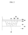
- FIG. 2 is a cross-sectional view of another exemplary embodiment of a LED according to the invention.
- the LED 1 according to the exemplary embodiment of FIG. 2 mostly has the same constitution as the LED according to the exemplary embodiment of FIG. 1 . Accordingly, only portions having differences from the LED according to the exemplary embodiment of FIG. 1 will be described. The remaining portions may be applied with the description of the exemplary embodiment of FIG. 1 .
- a coating layer 300 according to the illustrated exemplary embodiment includes a lower layer 300a, and an upper layer 300b positioned directly on the lower layer 300a.
- the upper layer 300b may include a material having a lower refractive index than the lower layer 300a.
- the coating layer 300 according to the illustrated exemplary embodiment is not limited to the dual-layer structure including the lower layer 300a and the upper layer 300b, and may include a plurality of layers having refractive indexes that are gradually decreased closer to the air from the encapsulation layer 200. The light efficiency may be further improved through this structure.
- the encapsulation layer 200 includes a lower encapsulation layer 200a covering all exposed surfaces of the light emitting unit 140, and an upper encapsulation layer 200b positioned directly on the lower encapsulation layer 200a.
- the upper encapsulation layer 200b may have a lower refractive index than the lower encapsulation layer 200a.
- the light emitting chip included in the light emitting unit 140 may include gallium nitride (GaN), whereby the refractive index of the light emitting unit 140 is about 2.32.
- GaN gallium nitride
- the refractive index of the lower encapsulation layer 200a may be about 2.0 and the refractive index of the upper encapsulation layer 200b may be about 1.7.
- the encapsulation layer 200 is not limited to the dual-layer structure including the lower encapsulation layer 200a and the upper encapsulation layer 200b, and may include a plurality of layers having refractive indexes that are gradually decreased closer to the coating layer 300 from the light emitting unit 140. The light efficiency may be further improved through this structure.
- FIG. 3 is a cross-sectional view of another exemplary embodiment of a LED according to the invention.
- the structure of the coating layer 300 covers an entire of an upper surface of the LED 1 and a portion of side surfaces of the package 150.
- the coating layer 300 may overlap an entire of the side surfaces of the package 150, or may only overlap a portion of the side surfaces as illustrated in FIG. 3 .
- the coating layer according to the exemplary embodiment of FIG. 1 only overlaps an entire of the upper surface of the LED 1.
- Upper and lateral portions of the coating layer 300 collectively form a single, unitary, indivisible member.
Landscapes
- Chemical & Material Sciences (AREA)
- Inorganic Chemistry (AREA)
- Engineering & Computer Science (AREA)
- Materials Engineering (AREA)
- Organic Chemistry (AREA)
- Led Device Packages (AREA)
- Electroluminescent Light Sources (AREA)
Abstract
Description
- The invention is a light emitting diode ("LED").
- A LED is basically made of a semiconductor junction of a p-type and an n-type, and is an element using a light emitting semiconductor emitting energy corresponding to a band gap of the semiconductor as a light formed by the combination of electrons and holes under a voltage application. The LED has various merits such as a small size and a light weight, a longer lifetime, less heat production, and a high response speed compared with a conventional light bulb, and thereby is used for various electrical and electronic products.
- The LED generally includes an LED chip, and a sealant to protect the LED chip. The sealant is conventionally formed of a material such as silicon resin, however it has weak protection against moisture.
- Also, the refractive index of the material used in the structure of the LED is much larger than the refractive index of the atmosphere such that reflection is seriously generated, thereby decreasing light efficiency.
- The above information disclosed in this Background section is only for enhancement of understanding of the background of the invention and therefore it may contain information that does not form the prior art that is already known in this country to a person of ordinary skill in the art.
- Exemplary embodiments of the present invention provides a light emitting diode ("LED") including a coating layer preventing light loss by reflection and having moisture resistance.
- A exemplary embodiment of the present invention provides a LED including a substrate, a light emitting unit on the substrate and generating light, an encapsulation layer covering the light emitting unit, and a coating layer including an organic material and on the encapsulation layer. A refractive index of the coating layer is greater than a refractive index of air and less than a refractive index of the encapsulation layer.
- The coating layer may include at least one of oleic acid, palmitic acid, eicosenoic acid, and erucic acid.
- The encapsulation layer may include a phosphor therein.
- The phosphor may be an oxide group compound or a nitride group compound.
- The phosphor may include a nitride crystal or oxynitride crystal including europium (Eu) among a crystal having a β type silicon nitride (Si3N4) crystal structure.
- The phosphor may include at least one of (Ba,Sr,Ca)2SiO4:Eu2+, Ba2MgSi2O7:Eu2+, Ba2ZnSi2O7:Eu2+, BaAl2O4:Eu2+, SrAl2O4:Eu2+, BaMgAl10O17:Eu2+, Mn2+, and BaMg2Al16O27:Eu2+ of a green wavelength range.
- The phosphor may include at least one of BaMg2Al16O27:EU2+, Sr4Al14O25:Eu2+, BaAl18O13:Eu2+, (Sr,Mg,Ca,Ba)5(PO4)3Cl:Eu2+, and Sr2Si3O8 - 2SrCl2:Eu2+ of a blue wavelength range.
- The phosphor may include at least one of Y2O3:Eu3+, Bi3+, (Sr,Ca,Ba,Mg,Zn)2P2O7:Eu2+, Mn2+, (Ca,Sr,Ba,Mg,Zn)10 (PO4)6(F,Cl,Br,OH)2:Eu2+, Mn2+, (Gd,Y,Lu,La)2O3:Eu3+, Bi3+, (Gd,Y,Lu,La)BO3:Eu3+, Bi3+, (Gd,Y, Lu, La) (P,V)O4:Eu3+, Bi3+, (Ba,Sr,Ca)MgP2O:Eu2+, Mn2+, (Y,Lu)2WO6:Eu3+, Mo6+, (Sr,Ca,Ba,Mg,Zn)2SiO4:Eu2+, and Mn2+ as an oxide group, or (Sr,Ca)AlSiN3:Eu2+, (Ba,Sr,Ca)2Si5N8:Eu2+, or (Ba,Sr,Ca)2Sio4-xNy:Eu2+ as a nitride group of a red wavelength range.
- The encapsulation layer may include an epoxy resin or silicon resin.
- The light which is generated by the light emitting unit may pass through the encapsulation layer and the coating layer in sequence.
- The coating layer may include a lower layer, and an upper layer disposed on the lower layer. The upper layer includes a material having a lower refractive index than a material of the lower layer.
- A mold frame may be on an upper surface of the substrate, and the light emitting unit and the encapsulation layer may be inside the mold frame.
- The coating layer may be extended from the encapsulation layer and may overlap a portion of a lateral side of the mold frame.
- The encapsulation layer may include dual layers having different refractive indexes.
- The encapsulation layer may include a lower encapsulation layer covering the light emitting unit, and an upper encapsulation layer on the lower encapsulation layer. A refractive index of the upper encapsulation layer is smaller than a refractive index of the lower encapsulation layer.
- In exemplary embodiments of the invention, the coating layer may include a material having strong moisture resistance. The coating layer reduces the difference between the refractive index of the LED and the refractive index of the atmosphere such that reliability and light efficiency may be simultaneously improved.
- The above and other features of this disclosure will become more apparent by describing in further detail exemplary embodiments thereof with reference to the accompanying drawings, in which:
-
FIG. 1 is a cross-sectional view of an exemplary embodiment of a light emitting diode ("LED") according to the invention. -
FIG. 2 is a cross-sectional view of another exemplary embodiment of a LED according to the invention. -
FIG. 3 is a cross-sectional view of another exemplary embodiment of a LED according to the invention. - The invention will be described more fully hereinafter with reference to the accompanying drawings, in which exemplary embodiments of the invention are shown. However, it is to be understood that the invention is not limited to the disclosed embodiments, but, on the contrary, is intended to cover various modifications. As those skilled in the art would realize, the described embodiments may be modified in various different ways, all without departing from the spirit or scope of the invention.
- In the drawings, the thickness of layers, films, panels, regions, etc., are exaggerated for clarity. It will be understood that when an element such as a layer, film, region, or substrate is referred to as being "on" another element, it can be directly on the other element or intervening elements may also be present. Like reference numerals designate like elements throughout the specification.
- It will be understood that, although the terms first, second, third, etc., may be used herein to describe various elements, components, regions, layers and/or sections, these elements, components, regions, layers and/or sections should not be limited by these terms. These terms are only used to distinguish one element, component, region, layer or section from another region, layer or section. Thus, a first element, component, region, layer or section discussed below could be termed a second element, component, region, layer or section without departing from the teachings of the invention.
- Spatially relative terms, such as "lower," "upper" and the like, may be used herein for ease of description to describe the relationship of one element or feature to another element(s) or feature(s) as illustrated in the figures. It will be understood that the spatially relative terms are intended to encompass different orientations of the device in use or operation, in addition to the orientation depicted in the figures. For example, if the device in the figures is turned over, elements described as "lower" relative to other elements or features would then be oriented "upper" relative to the other elements or features. Thus, the exemplary term "below" can encompass both an orientation of above and below. The device may be otherwise oriented (rotated 90 degrees or at other orientations) and the spatially relative descriptors used herein interpreted accordingly.
- The terminology used herein is for the purpose of describing particular embodiments only and is not intended to be limiting of the invention. As used herein, the singular forms "a," "an" and "the" are intended to include the plural forms as well, unless the context clearly indicates otherwise. It will be further understood that the terms "comprises" and/or "comprising," when used in this specification, specify the presence of stated features, integers, steps, operations, elements, and/or components, but do not preclude the presence or addition of one or more other features, integers, steps, operations, elements, components, and/or groups thereof.
- Embodiments of the invention are described herein with reference to cross-section illustrations that are schematic illustrations of idealized embodiments (and intermediate structures) of the invention. As such, variations from the shapes of the illustrations as a result, for example, of manufacturing techniques and/or tolerances, are to be expected. Thus, embodiments of the invention should not be construed as limited to the particular shapes of regions illustrated herein but are to include deviations in shapes that result, for example, from manufacturing.
- Unless otherwise defined, all terms (including technical and scientific terms) used herein have the same meaning as commonly understood by one of ordinary skill in the art to which this invention belongs. It will be further understood that terms, such as those defined in commonly used dictionaries, should be interpreted as having a meaning that is consistent with their meaning in the context of the relevant art and will not be interpreted in an idealized or overly formal sense unless expressly so defined herein.
- All methods described herein can be performed in a suitable order unless otherwise indicated herein or otherwise clearly contradicted by context. The use of any and all examples, or exemplary language (e.g., "such as"), is intended merely to better illustrate the invention and does not pose a limitation on the scope of the invention unless otherwise claimed. No language in the specification should be construed as indicating any non-claimed element as essential to the practice of the invention as used herein.
- Hereinafter, the invention will be described in detail with reference to the accompanying drawings.
-
FIG. 1 is a cross-sectional view of an exemplary embodiment of a light emitting diode ("LED") according to the invention. - Referring to
FIG. 1 , aLED 1 according to the illustrated exemplary embodiment includes asubstrate 100, amold frame 120 on and overlapping an outer part of thesubstrate 100, and alight emitting unit 140 positioned on an exposedportion substrate 100 enclosed by themold frame 120. Thesubstrate 100 and themold frame 120 may be integrally formed, such that thesubstrate 100 and themold frame 120 collectively form a single, unitary, indivisible member. - A
package 150 including thesubstrate 100 and themold frame 120 functions to protect thelight emitting unit 140 from external moisture. - The
LED 1 includes anencapsulation layer 200 completely filling the space between themold frame 120 and thelight emitting unit 140. Theencapsulation layer 200 includes aphosphor 180 dispersed therein. - Although not shown, the
light emitting unit 140 also includes a light emitting chip and a lead pattern, and may include wiring connecting the light emitting chip and the lead pattern to each other. The lead pattern as an electrode pattern functions to apply external power to the light emitting chip. - The light emitting chip as a horizontal type of light emitting chip in which an N-type electrode and a P-type electrode on a same plane is mounted on the lead pattern. A vertical type of light emitting chip including an upper P-type electrode and a lower N-type electrode may also be used.
- The
encapsulation layer 200 functions to protect thelight emitting unit 140 by encapsulating thelight emitting unit 140, and thephosphor 180 dispersed inside theencapsulation layer 200 includes green phosphor and red phosphor that are mixed, thereby emitting red and green light according when light is incident thereto. Thelight emitting unit 140 may be a blue light emitting chip, and blue light emitted from the blue light emitting chip, red light, and green light are mixed, thereby outputting white light. - The
phosphor 180 included in theLED 1 according to the illustrated exemplary embodiment may include an oxide group compound or a nitride group compound. Thephosphor 180 according to the illustrated exemplary embodiment may include a crystal of a nitride or an oxynitride including europium (Eu) among a crystal structure of a β type of silicon nitride (Si3N4). - The
phosphor 180 according to the illustrated exemplary embodiment may include at least one of (Ba,Sr,Ca)2SiO4-Eu2+, Ba2MgSi2O7:Eu2+, Ba2ZnSi2O7:Eu2 +, BaAl2O4:Eu2+, SrAl2O4:Eu2+, BaMgAl10O17:Eu2+, Mn2+, and BaMg2Al16O27:Eu2+ that are included in a green wavelength range. The materials for the above-describedphosphor 180 may be used alone or as a mixture. - The
phosphor 180 according to another exemplary embodiment may include at least one of BaMg2Al16O27:Eu2+, Sr4Al14O25:Eu2+,BaAl18O13:Eu2+, (Sr,Mg,Ca,Ba)5(PO4)3Cl:Eu2+, and Sr2Si3O8 · 2SrCl2:Eu2+ that are included in a blue wavelength range. - The
phosphor 180 according to another exemplary embodiment may include at least one of Y2O3:Eu3+, Bi3+, (Sr,Ca,Ba,Mg,Zn)2P2O7:Eu2+, Mn2+, (Ca,Sr,Ba,Mg,Zn)10(PO4)6(F,Cl,Br,OH)2:Eu2+, Mn2+, (Gd,Y,Lu,La)2O3:Eu3+, Bi3+, (Gd,Y,Lu,La)BO3:Eu3+, Bi3+, (Gd,Y,Lu,La)(P,V)O4:Eu3+, Bi3+, (Ba,Sr,Ca)MgP2O7:Eu2+, Mn2+, (Y,Lu)2WO6:Eu3+, Mo6+, (Sr,Ca,Ba,Mg,Zn)2SiO4:Eu2+ and Mn2+ among the oxide group, or (Sr,Ca)AlSiN3:Eu2+, (Ba,Sr,Ca)2Si5N8:Eu2+, and (Ba7Sr,Ca)2SiO4-xNy:Eu2+ among the nitride group, which are included in a red wavelength range. - The
phosphor 180 according to the illustrated exemplary embodiment including the materials described above has excellent thermal stability and optimized spectrum matching along with a color filter for a liquid crystal display ("LCD"), thereby realizing excellent luminance and color reproducibility. - The
encapsulation layer 200 may include a transparent silicon resin or epoxy resin, and an opaque resin of a degree that light may pass according to usage of the LED. - The
LED 1 according to the illustrated exemplary embodiment includes acoating layer 300 directly on theencapsulation layer 200. Thecoating layer 300 covers theencapsulation layer 200 and themold frame 120, and although not shown, thecoating layer 300 is extended to cover the side of thepackage 150. TheLED 1 includes a space formed by themold frame 120, thelight emitting unit 140 and thecoating layer 300, and theencapsulation layer 200 completely fills the space. - The
coating layer 300 according to the illustrated exemplary embodiment may include an organic material having a refractive index between the refractive index of thelight emitting unit 140 and the refractive index of the atmosphere. - The
coating layer 300 according to the illustrated exemplary embodiment may include at least one of oleic acid, palmitic acid, eicosenoic acid, and erucic acid shown in Table 1 below.[Table 1] Title Molecular formula Structure Refractive Index Oleic acid C18H34O2 
1.454 Palmitic acid C16H32O2 
1.425 Eicosenoic acid C20 H38O2 
1.456 Erucic acid C22H42O2 
1.457 - The materials of the
coating layer 300 according to the illustrated exemplary embodiment include many hydrophobic functional groups such that penetration of external moisture into thelight emitting unit 140 may be reduced or effectively prevented. As an experimental result, the luminance of a non-coated LED is 7.90 candelas (cd), however the luminance of a LED that is coated with oleic acid according to the illustrated exemplary embodiment is 8.24 cd, thereby being improved by about 4% over the non-coated LED. - Also, the
coating layer 300 has a refractive index between the refractive index of air of 1 and the refractive index of theencapsulation layer 200 including silicon resin of about 1.54, such that the degree of total reflection may be reduced when the light generated from thelight emitting unit 140 passes through theencapsulation layer 200 and is incident to the air. In other words, a critical angle (an angle at which total reflection is generated) by which the light generated by thelight emitting unit 140 passes through theencapsulation layer 200 and is emitted to the air may be increased. -
FIG. 2 is a cross-sectional view of another exemplary embodiment of a LED according to the invention. - The
LED 1 according to the exemplary embodiment ofFIG. 2 mostly has the same constitution as the LED according to the exemplary embodiment ofFIG. 1 . Accordingly, only portions having differences from the LED according to the exemplary embodiment ofFIG. 1 will be described. The remaining portions may be applied with the description of the exemplary embodiment ofFIG. 1 . - A
coating layer 300 according to the illustrated exemplary embodiment includes alower layer 300a, and anupper layer 300b positioned directly on thelower layer 300a. Theupper layer 300b may include a material having a lower refractive index than thelower layer 300a. Thecoating layer 300 according to the illustrated exemplary embodiment is not limited to the dual-layer structure including thelower layer 300a and theupper layer 300b, and may include a plurality of layers having refractive indexes that are gradually decreased closer to the air from theencapsulation layer 200. The light efficiency may be further improved through this structure. - The
encapsulation layer 200 according to the illustrated exemplary embodiment includes alower encapsulation layer 200a covering all exposed surfaces of thelight emitting unit 140, and anupper encapsulation layer 200b positioned directly on thelower encapsulation layer 200a. Here, theupper encapsulation layer 200b may have a lower refractive index than thelower encapsulation layer 200a. The light emitting chip included in thelight emitting unit 140 may include gallium nitride (GaN), whereby the refractive index of thelight emitting unit 140 is about 2.32. Here, the refractive index of thelower encapsulation layer 200a may be about 2.0 and the refractive index of theupper encapsulation layer 200b may be about 1.7. - The
encapsulation layer 200 according to the illustrated exemplary embodiment is not limited to the dual-layer structure including thelower encapsulation layer 200a and theupper encapsulation layer 200b, and may include a plurality of layers having refractive indexes that are gradually decreased closer to thecoating layer 300 from thelight emitting unit 140. The light efficiency may be further improved through this structure. -
FIG. 3 is a cross-sectional view of another exemplary embodiment of a LED according to the invention. - Referring to
FIG. 3 , the structure of thecoating layer 300 covers an entire of an upper surface of theLED 1 and a portion of side surfaces of thepackage 150. Thecoating layer 300 may overlap an entire of the side surfaces of thepackage 150, or may only overlap a portion of the side surfaces as illustrated inFIG. 3 . In contrast, the coating layer according to the exemplary embodiment ofFIG. 1 only overlaps an entire of the upper surface of theLED 1. Upper and lateral portions of thecoating layer 300 collectively form a single, unitary, indivisible member. - While this invention has been described in connection with what is presently considered to be practical exemplary embodiments, it is to be understood that the invention is not limited to the disclosed embodiments, but, on the contrary, is intended to cover various modifications and equivalent arrangements included within the spirit and scope of the appended claims.
Claims (15)
- A light emitting diode comprising:a substrate;a light emitting unit on the substrate and generating light;an encapsulation layer covering the light emitting unit; anda coating layer including an organic material and on the encapsulation layer,wherein a refractive index of the coating layer is greater than a refractive index of air and less than a refractive index of the encapsulation layer.
- The light emitting diode of claim 1, wherein
the coating layer includes at least one of oleic acid, palmitic acid, eicosenoic acid, and erucic acid. - The light emitting diode of claim 2, wherein
the encapsulation layer includes a phosphor therein. - The light emitting diode of claim 3, wherein
the phosphor is an oxide group compound or a nitride group compound. - The light emitting diode of claim 4, wherein
the phosphor includes a nitride crystal or oxynitride crystal comprising europium (Eu) among a crystal having a β type silicon nitride (Si3N4) crystal structure. - The light emitting diode of claim 4, wherein
the phosphor includes at least one of (Ba,Sr,Ca)2SiO4:Eu2+, Ba2MgSi2O7:Eu2+, Ba2ZnSi2O7:Eu2+, BaAl2O4:Eu2+, SrAl2O4:Eu2+, BaMgAl10O17:Eu2+, Mn2+, and BaMg2Al16O27:Eu2+ of a green wavelength range. - The light emitting diode of claim 4, wherein
the phosphor includes at least one of BaMg2Al16O27:Eu2+, Sr4Al14O25:Eu2+, BaAl18O13:Eu2+, (Sr,Mg,Ca,Ba)5(PO4)3Cl:Eu2+, and Sr2Si3O8 - 2SrCl2:Eu2+ of a blue wavelength range. - The light emitting diode of claim 4, wherein
the phosphor includes at least one of Y2O3:Eu3+, Bi3+,
(Sr,Ca,Ba,Mg,Zn)2P2O7:Eu2 +, Mn2+, (Ca,Sr,Ba,Mg,Zn)10(PO4)6(F,Cl,Br,OH)2:Eu2+, Mn2+, (Gd,Y,Lu,La)2O3:Eu3+, Bi3+, (Gd,Y,Lu,La)BO3:Eu3+, Bi3+, (Gd,Y,Lu,La)(P,V)O4:Eu3+, Bi3+, (Ba,Sr,Ca)MgP2O7:Eu2+, Mn2+, (Y,Lu)2WO6:Eu3+, Mo6+, (Sr,Ca,Ba,Mg,Zn)2SiO4:Eu2+, and Mn2+ as an oxide group, or (Sr,Ca)AlSiN3:Eu2+, (Ba,Sr,Ca)2Si5N8:Eu2+, or (Ba,Sr,Ca)2SiO4-xNy:Eu2+ as a nitride group of a red wavelength range. - The light emitting diode of claim 1, wherein
the encapsulation layer includes an epoxy resin or silicon resin. - The light emitting diode of claim 9, wherein
the light which is generated by the light emitting unit passes through the encapsulation layer and the coating layer in sequence. - The light emitting diode of claim 1, wherein
the coating layer includes a lower layer, and an upper layer disposed on the lower layer, and
the upper layer includes a material having a lower refractive index than a material of the lower layer. - The light emitting diode of claim 1,
further comprising a mold frame on an upper surface of the substrate,
and
the light emitting unit and the encapsulation layer are inside the mold frame. - The light emitting diode of claim 12, wherein
the coating layer is extended from the encapsulation layer and overlaps a portion of a lateral side of the mold frame. - The light emitting diode of claim 1, wherein
the encapsulation layer includes dual layers having different refractive indexes. - The light emitting diode of claim 14, wherein
the encapsulation layer includes a lower encapsulation layer covering the light emitting unit, and
an upper encapsulation layer on the lower encapsulation layer, and
a refractive index of the upper encapsulation layer is smaller than a refractive index of the lower encapsulation layer.
Applications Claiming Priority (1)
| Application Number | Priority Date | Filing Date | Title |
|---|---|---|---|
| KR1020110017063A KR20120097697A (en) | 2011-02-25 | 2011-02-25 | Light emitting diode |
Publications (2)
| Publication Number | Publication Date |
|---|---|
| EP2492977A2 true EP2492977A2 (en) | 2012-08-29 |
| EP2492977A3 EP2492977A3 (en) | 2014-01-08 |
Family
ID=44508833
Family Applications (1)
| Application Number | Title | Priority Date | Filing Date |
|---|---|---|---|
| EP11174876.0A Withdrawn EP2492977A3 (en) | 2011-02-25 | 2011-07-21 | Light emitting diode |
Country Status (5)
| Country | Link |
|---|---|
| US (1) | US20120217522A1 (en) |
| EP (1) | EP2492977A3 (en) |
| JP (1) | JP5823228B2 (en) |
| KR (1) | KR20120097697A (en) |
| CN (1) | CN102651447B (en) |
Families Citing this family (4)
| Publication number | Priority date | Publication date | Assignee | Title |
|---|---|---|---|---|
| JP2016001702A (en) * | 2014-06-12 | 2016-01-07 | 大日本印刷株式会社 | Lead frame with resin and method for manufacturing the same, and led package and method for manufacturing the same |
| CN104124326B (en) * | 2014-08-13 | 2017-02-22 | 弗洛里光电材料(苏州)有限公司 | Semiconductor light emitting device optical encapsulation structure |
| KR101706843B1 (en) * | 2015-03-20 | 2017-02-16 | 전남대학교산학협력단 | Phosphor, Method of fabricating the same, and Light Emitting Device of using the same |
| KR102626391B1 (en) * | 2018-02-27 | 2024-01-17 | 삼성디스플레이 주식회사 | Display device |
Family Cites Families (17)
| Publication number | Priority date | Publication date | Assignee | Title |
|---|---|---|---|---|
| JPH06151977A (en) * | 1992-11-11 | 1994-05-31 | Sharp Corp | Optical semiconductor device |
| DE10220583B4 (en) * | 2002-03-27 | 2007-07-05 | Osram Opto Semiconductors Gmbh | Optoelectronic component |
| US6809471B2 (en) * | 2002-06-28 | 2004-10-26 | General Electric Company | Phosphors containing oxides of alkaline-earth and Group-IIIB metals and light sources incorporating the same |
| US7224000B2 (en) * | 2002-08-30 | 2007-05-29 | Lumination, Llc | Light emitting diode component |
| US6924233B1 (en) * | 2004-03-19 | 2005-08-02 | Agilent Technologies, Inc. | Phosphor deposition methods |
| JP2006135225A (en) * | 2004-11-09 | 2006-05-25 | Toshiba Corp | Light emitting device |
| WO2007018039A1 (en) * | 2005-08-05 | 2007-02-15 | Matsushita Electric Industrial Co., Ltd. | Semiconductor light-emitting device |
| JP2007116131A (en) * | 2005-09-21 | 2007-05-10 | Sanyo Electric Co Ltd | LED light emitting device |
| JP4415972B2 (en) * | 2005-09-22 | 2010-02-17 | ソニー株式会社 | Method for producing metal oxide nanoparticles |
| WO2007088501A1 (en) * | 2006-01-31 | 2007-08-09 | Koninklijke Philips Electronics N.V. | White light source |
| US7655486B2 (en) * | 2006-05-17 | 2010-02-02 | 3M Innovative Properties Company | Method of making light emitting device with multilayer silicon-containing encapsulant |
| CA2600900A1 (en) * | 2006-09-21 | 2008-03-21 | Nippon Sheet Glass Company, Limited | Transmissive diffraction grating, and spectral separation element and spectroscope using the same |
| US20090032088A1 (en) * | 2007-08-03 | 2009-02-05 | Mario Rabinowitz | Sealants for Solar Energy Concentrators and Similar Equipment |
| KR101592836B1 (en) * | 2008-02-07 | 2016-02-05 | 미쓰비시 가가꾸 가부시키가이샤 | Semiconductor light emitting device, backlighting device, color image display device and phosphor used for those devices |
| JP5766386B2 (en) * | 2008-08-29 | 2015-08-19 | 株式会社東芝 | Light emitting device and light emitting device |
| KR100982990B1 (en) * | 2008-09-03 | 2010-09-17 | 삼성엘이디 주식회사 | wavelength conversion plate and light emitting device using the same |
| WO2010126606A2 (en) * | 2009-05-01 | 2010-11-04 | Nanosys, Inc. | Functionalized matrixes for dispersion of nanostructures |
-
2011
- 2011-02-25 KR KR1020110017063A patent/KR20120097697A/en not_active Abandoned
- 2011-07-05 US US13/176,150 patent/US20120217522A1/en not_active Abandoned
- 2011-07-21 EP EP11174876.0A patent/EP2492977A3/en not_active Withdrawn
- 2011-09-27 JP JP2011210444A patent/JP5823228B2/en not_active Expired - Fee Related
- 2011-10-10 CN CN201110305126.6A patent/CN102651447B/en not_active Expired - Fee Related
Non-Patent Citations (1)
| Title |
|---|
| None |
Also Published As
| Publication number | Publication date |
|---|---|
| CN102651447A (en) | 2012-08-29 |
| EP2492977A3 (en) | 2014-01-08 |
| KR20120097697A (en) | 2012-09-05 |
| CN102651447B (en) | 2016-05-04 |
| US20120217522A1 (en) | 2012-08-30 |
| JP5823228B2 (en) | 2015-11-25 |
| JP2012178540A (en) | 2012-09-13 |
Similar Documents
| Publication | Publication Date | Title |
|---|---|---|
| US9634203B2 (en) | Light emitting device, surface light source, liquid crystal display device, and method for manufacturing light emitting device | |
| CN102110682B (en) | Light-emitting device and method for producing the same | |
| US9831396B2 (en) | Light emitting device including light emitting element with phosphor | |
| JP6549165B2 (en) | Light source device and light emitting device | |
| JP6149487B2 (en) | LIGHT EMITTING DEVICE MANUFACTURING METHOD AND LIGHT EMITTING DEVICE | |
| EP3410497B1 (en) | Light-emitting device and method of manufacturing same | |
| US20190348580A1 (en) | Light emitting device | |
| US11313536B2 (en) | Light emitting device | |
| US11489099B2 (en) | Light-emitting device | |
| US11664406B2 (en) | Light-emitting device | |
| KR20150007885A (en) | Phosphor and light emitting device having thereof | |
| KR20120025367A (en) | Light emitting device | |
| EP2492977A2 (en) | Light emitting diode | |
| US7804237B2 (en) | Luminescence conversion of LED including two phosphors | |
| KR102512806B1 (en) | Light emitting device and preparation method thereof | |
| US8994049B2 (en) | Light emitting component and manufacturing method thereof | |
| KR102509024B1 (en) | Light emitting device and lighting apparatus having thereof | |
| EP2682447A2 (en) | Method of manufacturing nanophosphors, light emitting diode and method of manufacturing light emitting diode | |
| KR102135626B1 (en) | Light emitting device having uv light diode | |
| KR20140063066A (en) | Phosphor compositions | |
| KR20140063067A (en) | Phosphor compositions | |
| JP2017220530A (en) | Manufacturing method of light-emitting device |
Legal Events
| Date | Code | Title | Description |
|---|---|---|---|
| PUAI | Public reference made under article 153(3) epc to a published international application that has entered the european phase |
Free format text: ORIGINAL CODE: 0009012 |
|
| 17P | Request for examination filed |
Effective date: 20120329 |
|
| AK | Designated contracting states |
Kind code of ref document: A2 Designated state(s): AL AT BE BG CH CY CZ DE DK EE ES FI FR GB GR HR HU IE IS IT LI LT LU LV MC MK MT NL NO PL PT RO RS SE SI SK SM TR |
|
| AX | Request for extension of the european patent |
Extension state: BA ME |
|
| RAP1 | Party data changed (applicant data changed or rights of an application transferred) |
Owner name: SAMSUNG ELECTRONICS CO., LTD. |
|
| RAP1 | Party data changed (applicant data changed or rights of an application transferred) |
Owner name: SAMSUNG DISPLAY CO., LTD. |
|
| PUAL | Search report despatched |
Free format text: ORIGINAL CODE: 0009013 |
|
| AK | Designated contracting states |
Kind code of ref document: A3 Designated state(s): AL AT BE BG CH CY CZ DE DK EE ES FI FR GB GR HR HU IE IS IT LI LT LU LV MC MK MT NL NO PL PT RO RS SE SI SK SM TR |
|
| AX | Request for extension of the european patent |
Extension state: BA ME |
|
| RIC1 | Information provided on ipc code assigned before grant |
Ipc: H01L 33/44 20100101AFI20131205BHEP Ipc: H01L 33/56 20100101ALN20131205BHEP Ipc: H01L 33/50 20100101ALN20131205BHEP |
|
| RAP1 | Party data changed (applicant data changed or rights of an application transferred) |
Owner name: SAMSUNG DISPLAY CO., LTD. |
|
| 17Q | First examination report despatched |
Effective date: 20160224 |
|
| STAA | Information on the status of an ep patent application or granted ep patent |
Free format text: STATUS: THE APPLICATION IS DEEMED TO BE WITHDRAWN |
|
| 18D | Application deemed to be withdrawn |
Effective date: 20180201 |