EP2492926A1 - Resistive voltage divider with high voltage ratio - Google Patents
Resistive voltage divider with high voltage ratio Download PDFInfo
- Publication number
- EP2492926A1 EP2492926A1 EP11001577A EP11001577A EP2492926A1 EP 2492926 A1 EP2492926 A1 EP 2492926A1 EP 11001577 A EP11001577 A EP 11001577A EP 11001577 A EP11001577 A EP 11001577A EP 2492926 A1 EP2492926 A1 EP 2492926A1
- Authority
- EP
- European Patent Office
- Prior art keywords
- trace
- resistor
- voltage divider
- resistors
- voltage
- Prior art date
- Legal status (The legal status is an assumption and is not a legal conclusion. Google has not performed a legal analysis and makes no representation as to the accuracy of the status listed.)
- Granted
Links
Images


Classifications
-
- H—ELECTRICITY
- H01—ELECTRIC ELEMENTS
- H01C—RESISTORS
- H01C13/00—Resistors not provided for elsewhere
- H01C13/02—Structural combinations of resistors
-
- G—PHYSICS
- G01—MEASURING; TESTING
- G01R—MEASURING ELECTRIC VARIABLES; MEASURING MAGNETIC VARIABLES
- G01R15/00—Details of measuring arrangements of the types provided for in groups G01R17/00 - G01R29/00, G01R33/00 - G01R33/26 or G01R35/00
- G01R15/04—Voltage dividers
-
- H—ELECTRICITY
- H01—ELECTRIC ELEMENTS
- H01C—RESISTORS
- H01C17/00—Apparatus or processes specially adapted for manufacturing resistors
- H01C17/22—Apparatus or processes specially adapted for manufacturing resistors adapted for trimming
- H01C17/23—Apparatus or processes specially adapted for manufacturing resistors adapted for trimming by opening or closing resistor geometric tracks of predetermined resistive values, e.g. snapistors
-
- H—ELECTRICITY
- H01—ELECTRIC ELEMENTS
- H01C—RESISTORS
- H01C7/00—Non-adjustable resistors formed as one or more layers or coatings; Non-adjustable resistors made from powdered conducting material or powdered semi-conducting material with or without insulating material
-
- H—ELECTRICITY
- H02—GENERATION; CONVERSION OR DISTRIBUTION OF ELECTRIC POWER
- H02M—APPARATUS FOR CONVERSION BETWEEN AC AND AC, BETWEEN AC AND DC, OR BETWEEN DC AND DC, AND FOR USE WITH MAINS OR SIMILAR POWER SUPPLY SYSTEMS; CONVERSION OF DC OR AC INPUT POWER INTO SURGE OUTPUT POWER; CONTROL OR REGULATION THEREOF
- H02M3/00—Conversion of DC power input into DC power output
- H02M3/02—Conversion of DC power input into DC power output without intermediate conversion into AC
- H02M3/04—Conversion of DC power input into DC power output without intermediate conversion into AC by static converters
- H02M3/06—Conversion of DC power input into DC power output without intermediate conversion into AC by static converters using resistors or capacitors, e.g. potential divider
-
- H—ELECTRICITY
- H02—GENERATION; CONVERSION OR DISTRIBUTION OF ELECTRIC POWER
- H02M—APPARATUS FOR CONVERSION BETWEEN AC AND AC, BETWEEN AC AND DC, OR BETWEEN DC AND DC, AND FOR USE WITH MAINS OR SIMILAR POWER SUPPLY SYSTEMS; CONVERSION OF DC OR AC INPUT POWER INTO SURGE OUTPUT POWER; CONTROL OR REGULATION THEREOF
- H02M5/00—Conversion of AC power input into AC power output, e.g. for change of voltage, for change of frequency, for change of number of phases
- H02M5/02—Conversion of AC power input into AC power output, e.g. for change of voltage, for change of frequency, for change of number of phases without intermediate conversion into DC
- H02M5/04—Conversion of AC power input into AC power output, e.g. for change of voltage, for change of frequency, for change of number of phases without intermediate conversion into DC by static converters
- H02M5/06—Conversion of AC power input into AC power output, e.g. for change of voltage, for change of frequency, for change of number of phases without intermediate conversion into DC by static converters using impedances
-
- H—ELECTRICITY
- H03—ELECTRONIC CIRCUITRY
- H03L—AUTOMATIC CONTROL, STARTING, SYNCHRONISATION OR STABILISATION OF GENERATORS OF ELECTRONIC OSCILLATIONS OR PULSES
- H03L7/00—Automatic control of frequency or phase; Synchronisation
- H03L7/06—Automatic control of frequency or phase; Synchronisation using a reference signal applied to a frequency- or phase-locked loop
- H03L7/08—Details of the phase-locked loop
- H03L7/085—Details of the phase-locked loop concerning mainly the frequency- or phase-detection arrangement including the filtering or amplification of its output signal
- H03L7/087—Details of the phase-locked loop concerning mainly the frequency- or phase-detection arrangement including the filtering or amplification of its output signal using at least two phase detectors or a frequency and phase detector in the loop
Definitions
- the invention relates to a resistive voltage divider which comprises at least a first and a second resistor electrically connected in series and made of an electrically resistive film material applied in form of a trace onto an insulating substrate and where the divider's voltage ratio has a value between one hundred and one million.
- the voltage divider may consist in its simplest form of just two serial resistors, one with a high resistance value and the other with a low resistance value.
- the one or both of the serial resistors can be replaced by resistive networks having respective equivalent resistance values. These resistors or corresponding resistor networks may in the following also be called high and low ohmic resistors, respectively.
- resistors by bringing a noninsulating, electrically resistive film or foil material, such as metal film or metal foil, e.g. nickel chromium, cermet film , e.g. tantalum nitride, ruthenium dioxide, bismuth ruthenate, carbon film, or a film of composite material based on a mixture of glass and cermet onto an insulating substrate.
- a noninsulating, electrically resistive film or foil material such as metal film or metal foil, e.g. nickel chromium, cermet film , e.g. tantalum nitride, ruthenium dioxide, bismuth ruthenate, carbon film, or a film of composite material based on a mixture of glass and cermet onto an insulating substrate.
- the electrically resistive film material may consist of multiple layers of different of the above named materials.
- the insulating substrate can be ceramic, silicon, glass or some other synthetic material, and the film material is applied to the substrate by methods such as sputtering (thin film), screen and stencil printing (thick film) or direct printing through a nozzle (thick film).
- the insulating substrate may have the form of a flat planar sheet or of a cylinder, and accordingly the resistive film is deposited either onto a two-dimensional planar surface or onto a three-dimensional axially symmetric surface.
- both the high and low ohmic resistors are brought onto the same substrate.
- highly conductive structures with considerable lower resistivity than the film material of the resistors are deposited on the substrate as well.
- the highly conductive structures are intended to be used as contacting terminals, and they are placed on the substrate in such a way that the resistive film material of the resistors overlaps partly with them.
- meandering form means that the trace is not just a straight line but curved in such a way that a long length is achieved on a small substrate area.
- the meandering form may look for example like a square wave, a triangle wave, a sine wave or something more irregular like a serpentine, a zigzag or - in the three-dimensional case - a helical form.
- the low resistance value of the low ohmic resistor is commonly obtained by arranging the resistive film material in a short and wide trace.
- the above described resistive voltage dividers can be used for a wide range of voltage levels, from low over medium up to high voltage applications. While the present invention originates from the area of medium voltage sensors, such as the KEVCD and KEVA sensor types by ABB, which are commonly applicable to a voltage range between 3.6 kV and 36 kV, its area of application is not limited to this voltage range.
- resistive voltage divider as described above which has a voltage ratio up to one million and is compact in its size.
- the high voltage ratio is significantly increased by replacing the commonly known short and wide trace of the low ohmic resistor by a network of at least two resistors electrically connected in parallel.
- the invention suggests arranging the two contacting terminals of the low ohmic resistor in an interdigitated manner, without the terminals touching each other of course.
- the traces of the two resistors each overlap at their respective ends with one of the contacting terminals, either partly or fully.
- the two contacting terminals are both arranged in a kind of comb-shaped form, their teeth being arranged in an interdigitated manner without touching each other and the multiple resistors are placed between the teeth and overlap with the teeth.
- these two resistors are arranged in the following way.
- the trace of the second resistor overlaps on one end at least in part with a first protrusion of a first contacting terminal and on the other end with a first boundary of a first recess provided in a second contacting terminal
- the trace of the third resistor overlaps on one end at least in part with the first protrusion and on the other end with a second boundary of the first recess, where the first and the second boundaries face each other.
- any suitable number of further resistors can be placed in parallel with the second and third resistors by just adding more teeth to the comb-shapes of the two contacting terminals.
- the invention suggests that in addition the trace of a fourth resistor overlaps on one end at least in part with the second boundary of the first recess and on the other end with a second protrusion of the first contacting terminal.
- An embodiment with four parallel resistors is achieved by arranging a fifth resistor such that its trace overlaps on one end at least in part with the second protrusion and on the other end with a third boundary of a second recess provided in the second contacting terminal, where the second and third boundaries face each other and are both part of the second recess.
- High voltage ratios can also be achieved by using significantly different resistive film materials for the high and low ohmic resistors, as is known from the art. However, this results in additional process steps and errors during the manufacturing of the voltage divider and accordingly in increased costs and reduced accuracy.
- the inventors have realized that the use of different resistive film materials in addition deteriorates the initial accuracy, the temperature stability and the long term stability of the voltage ratio. This is due to the fact that with different materials it is more difficult to achieve good initial accuracy of the voltage ratio, so that post-processing operations, such as laser trimming of one or of both the high and low ohmic resistors, are required to adjust the accuracy. Furthermore, it can no longer be ensured that the drifting of the operating characteristics of both the high and the low ohmic resistors occur in the same direction and with possibly the same amount so that the ratio of the resistance values and thereby the divider's voltage ratio can no longer be maintained at its initial value over changing temperature or over a long period of time.
- the parallel resistor traces of the low ohmic resistor may have differing lengths, depending on the distances between the teeth of the comb-shaped contacting terminals.
- the second and further resistors have a similar trace length, meaning that the trace lengths may vary within certain limits around a predefined average trace length.
- a preferred limit is that the shortest trace length may not be shorter than half of the longest trace length.
- a further advantage can be achieved when the drifting characteristics of the high and low ohmic resistors in the voltage divider are matched even further, thereby allowing for a further improved temperature stability and long term stability of the voltage ratio.
- Using the same resistive film material is already a first important step in that direction.
- the inventors have taken into account different effects, which may influence the initial value and/or the drifting characteristics of the voltage ratio.
- further embodiments of the invention are described, where the high and low ohmic resistors are designed in such a way that the effects occur in all resistors to possibly the same extent.
- edge effect occurring at the lateral edges of the trace.
- the lateral edges of the trace are usually not straight and cut sharply, but rather gradually decreasing towards the outer ends.
- the composition and/or the structure of the electrically resistive film material are slightly altered with respect to the region in the middle of the trace. Accordingly, it can be noted that with decreasing trace width the edge effect plays a larger role in affecting the trace resistance per unit length compared to the expected resistance of an ideal trace with rectangular cross section and homogenous composition and structure.
- the resistors In order to have the same amount of influence of the edge effect on the resistance value of the high and low ohmic resistors, it is therefore advantageous to provide the resistors with the same trace width, thereby ensuring superior matching of their resistance values and accordingly improved initial accuracy, temperature stability and long term stability.
- it is suggested to design the high and low ohmic resistors such that they have a similar trace width, meaning that the trace widths may vary within certain limits around a predefined average trace width.
- a preferred limit is that the narrowest trace width may not be narrower than half of the widest trace width.
- the high and low ohmic resistors have preferably the same trace width
- This concept can be extended as far as required by design criteria of the voltage divider, i.e. multiple rows of resistor traces may be placed geometrically in parallel, all of them overlapping with the teeth of the comb-shapes of the contacting terminals.
- Anisotropic stresses may be more pronounced for three-dimensional, e.g. cylindrical, voltage dividers, than for two-dimensional, flat voltage dividers.
- the term dominant trace segment is used for those parts of a meandering trace which are of considerable length, opposed to just the bends, and which have the highest impact on the overall resistance value of that trace compared to other trace segments. In case of a straight line, the dominant trace segment and the trace itself are the same.
- the voltage divider of Fig. 1 is known from the art, where the high ohmic resistor with a resistance value R 1 has a long and narrow trace with multiple bends and where the low ohmic resistor with a resistance value R 2 has a short and wide trace.
- the high ohmic resistor is placed between a third contacting terminal A and a first contacting terminal B and the low ohmic resistor between the first contacting terminal B and a second contacting terminal C.
- the resistive film material used for the high and low ohmic resistors differs here.
- FIG. 2 An equivalent schematic electrical diagram of the voltage divider of Fig. 1 is shown in Fig. 2 .
- a voltage divider is for example used in voltage sensors for the medium voltage range between 3.6 kV and 36 kV, such as the KEVCD and KEVA sensor types by ABB.
- an input voltage U in which represents the quantity to be measured, is applied between the third and second contacting terminals A and C, and an output voltage U out , having a much smaller value usually reduced by a factor equal to the voltage divider's ratio (R 1 + R 2 )/R 2 , is then delivered to an electronic circuitry in order to be processed and transformed into a measurement value.
- a first embodiment of the invention is schematically shown in Fig. 3 , where the high ohmic resistor and the low ohmic resistor are made of the same electrically resistive film material and where the resistance value R 4 of the low ohmic resistor is achieved by a network of two electrically parallel resistors.
- the high ohmic resistor may also be called first resistor and has a resistance value R 3 .
- the first contacting terminal B has a first protrusion 2 which extends into a first recess made within the second contacting terminal C, where the first recess has a first boundary 1 and a second boundary 3 that face each other.
- a wide and straight trace line extends from the first boundary 1 across the first protrusion 2 to the second boundary 3 and overlaps partly with the boundaries, thereby forming a second resistor between first boundary 1 and first protrusion 2 and a third resistor between first protrusion 2 and second boundary 3.
- the second and third resistors are electrically connected in parallel, as is shown in the schematic electrical diagram of Fig. 4 .
- the resulting resistance value of this parallel connection is the resistance value R 4 of the low ohmic resistor, and the voltage ratio of the divider is (R 3 + R 4 )/R 4 .
- the resistance value R 4 is decreased compared to R 2 of Fig.
- a second, third and fourth embodiment are shown, where the voltage ratio is further increased by connecting a fourth and fifth resistor in parallel with the second and third resistors.
- a second protrusion 4 extends into a second recess having a third boundary 5 and sharing the second boundary 3 with the first recess. From Figs. 5, 6 and 7 , it becomes apparent that the first and second contacting terminals B and C have a comb-shaped form with their teeth being arranged in an interdigitated manner without touching each other.
- a thick and straight trace line extends between the outer boundaries, here the first boundary 1 and the third boundary 5, overlapping with them in part as well as overlapping wholly with the inner boundary 3 and the two protrusions 2 and 4.
- the second resistor 12 (see Fig. 6 ) is again formed between the first protrusion 2 and the first boundary 1and the third resistor 13 is formed between the first protrusion 2 and the second boundary 3.
- the fourth resistor 14 is formed between the second boundary 3 and the second protrusion 4 and the fifth resistor 15 between the second protrusion 4 and the third boundary 5.
- the trace of the high ohmic resistor which is also called the first resistor is indicated in Fig. 6 by reference 10.
- the resistance value R 6 of the low ohmic resistor which is made up by the parallel network of the second, third, fourth and fifth resistors, is further reduced compared to the resistance value R 4 of the first embodiment, thereby increasing the voltage ratio (R 5 + R 6 )/R 6 .
- the high ohmic resistors in Figs. 5, 6 and 7 are no longer formed as a square wave, but as meandering forms with round corners at the bends. Accordingly, the corresponding resistance values R 5 , R 7 and R 9 , respectively, differ slightly from the resistance value R 3 of the first embodiment.
- the dominant traces 6 of the high ohmic resistor in Fig. 5 include with the resistor traces 11 of the low ohmic resistor an angle of zero degrees.
- this angle has a value above zero and below thirty degrees.
- the fourth embodiment of Fig. 7 shows a special design solution for the interface areas between the trace of the high ohmic resistor and the third and first contacting terminals A and B.
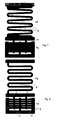
- the fifth embodiment shown in Fig. 8 differs from the second embodiment of Fig. 5 in that the low ohmic resistor is formed by the electrical network of twenty resistors connected in parallel. This is achieved by placing four further trace lines geometrically in parallel with the trace line 7 which comprises the second, third, fourth and fifth resistors.
- the resistive film material of the resistor traces overlaps at least in part with the corresponding contacting terminals A, B and C, respectively, by being placed on top of the contacting terminals.
- the overlap may of course be achieved by putting the contacting terminals on top.
- Fig. 8 shows a schematic cross-section view of a real resistor trace depicted with a solid line, compared to an ideal resistor trace shown with a dotted line.
- Reference 8 indicates the resistive film material and reference 9 the insulating substrate.
- the arrows indicate the areas at the edges of the trace width where the so called edge effects occur. The size of these areas is approximately the same for all trace widths which means that the real resistance value differs more from the ideal resistance value for smaller trace widths.
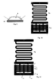
- Figs. 9 shows a schematic cross-section view of a real resistor trace depicted with a solid line, compared to an ideal resistor trace shown with a dotted line.
- Reference 8 indicates the resistive film material and reference 9 the insulating substrate.
- the arrows indicate the areas at the edges of the trace width where the so called edge effects occur. The size of these areas is approximately the same for all trace widths which means that the real resistance value differs more from the ideal resistance value for smaller trace widths.
- both the high and low ohmic resistors of Fig. 8 are provided with the same trace width.
- Figs. 10 and 11 the voltage divider according to a sixth and seventh embodiment, respectively, is shown.
- one of the resistor traces belonging to the low ohmic resistor is interrupted by cutting it in two pieces, as indicated by the solid arrow. In that way, one of the resistors of the corresponding parallel resistor network is eliminated, thereby increasing the resistance value by one increment from the value R 8 (see Fig. 8 ) to the value R 10 .
- the second protrusion 4 is cut in two pieces, thereby eliminating all the eight resistors which overlap with the second protrusion 4 from the resistor network, resulting in a resistance value R 11 which is twice as big as the value R 8 .
- the adjustment of the resistance value of a film resistor by erasing part of the resistive film material is known in the art as trimming. It may be noted that the design of the low ohmic resistor as a network of parallel resistor traces allows the trimming in a kind of digital manner by taking away whole resistors from the resistor network, opposed to analogue trimming which is achieved by erasing the resistive film material of a resistor trace only partly, as for example described in US 7,079,004 . Analogue trimming leaves behind cutting edges within the resistor's film material which may alter the microstructure of the material and may induce stresses, both usually affecting the stability of the resistance value. These negative effects can be avoided by applying digital trimming instead.
Landscapes
- Engineering & Computer Science (AREA)
- Microelectronics & Electronic Packaging (AREA)
- Physics & Mathematics (AREA)
- Power Engineering (AREA)
- Manufacturing & Machinery (AREA)
- General Physics & Mathematics (AREA)
- Electromagnetism (AREA)
- Non-Adjustable Resistors (AREA)
- Semiconductor Integrated Circuits (AREA)
- Stabilization Of Oscillater, Synchronisation, Frequency Synthesizers (AREA)
- Apparatuses And Processes For Manufacturing Resistors (AREA)
Abstract
Description
- The invention relates to a resistive voltage divider which comprises at least a first and a second resistor electrically connected in series and made of an electrically resistive film material applied in form of a trace onto an insulating substrate and where the divider's voltage ratio has a value between one hundred and one million. The voltage divider may consist in its simplest form of just two serial resistors, one with a high resistance value and the other with a low resistance value. In more advanced cases, the one or both of the serial resistors can be replaced by resistive networks having respective equivalent resistance values. These resistors or corresponding resistor networks may in the following also be called high and low ohmic resistors, respectively.
- Different techniques are known to manufacture resistors by bringing a noninsulating, electrically resistive film or foil material, such as metal film or metal foil, e.g. nickel chromium, cermet film , e.g. tantalum nitride, ruthenium dioxide, bismuth ruthenate, carbon film, or a film of composite material based on a mixture of glass and cermet onto an insulating substrate. In rare cases, the electrically resistive film material may consist of multiple layers of different of the above named materials. The insulating substrate can be ceramic, silicon, glass or some other synthetic material, and the film material is applied to the substrate by methods such as sputtering (thin film), screen and stencil printing (thick film) or direct printing through a nozzle (thick film). The insulating substrate may have the form of a flat planar sheet or of a cylinder, and accordingly the resistive film is deposited either onto a two-dimensional planar surface or onto a three-dimensional axially symmetric surface. In the voltage divider, both the high and low ohmic resistors are brought onto the same substrate. In addition, highly conductive structures with considerable lower resistivity than the film material of the resistors are deposited on the substrate as well. The highly conductive structures are intended to be used as contacting terminals, and they are placed on the substrate in such a way that the resistive film material of the resistors overlaps partly with them.
- In order to achieve voltage ratios of significantly more than unity and at the same time to reduce the size of the voltage divider, it is known to arrange the resistive film material of the high ohmic resistor in a long and narrow trace, where the trace is shaped like a meandering form. The term meandering form means that the trace is not just a straight line but curved in such a way that a long length is achieved on a small substrate area. The meandering form may look for example like a square wave, a triangle wave, a sine wave or something more irregular like a serpentine, a zigzag or - in the three-dimensional case - a helical form. This is for example described in
US 5,521,576 for thick film resistors and inUS 7,079,004 B2 for thin film AC voltage dividers. As is disclosed there as well, the low resistance value of the low ohmic resistor is commonly obtained by arranging the resistive film material in a short and wide trace. - In general, the above described resistive voltage dividers can be used for a wide range of voltage levels, from low over medium up to high voltage applications. While the present invention originates from the area of medium voltage sensors, such as the KEVCD and KEVA sensor types by ABB, which are commonly applicable to a voltage range between 3.6 kV and 36 kV, its area of application is not limited to this voltage range.
- For medium and high voltage applications of up to one megavolt, voltage ratios of up to several hundred thousand are commonly required in order to step down the quantity which is to be measured to the voltage level of the processing electronics. A possibility to achieve higher voltage ratios is to increase the length of the high ohmic resistor. However, there are limits with respect to the available substrate area and the acceptable size of the voltage divider. It is also possible to reduce the length of the trace of the low ohmic resistor. However, there are technological limitations for the minimum trace length and for the minimum spacing between the connecting terminals. Even though these possibilities exist, it needs to be ascertained that currently, resistive dividers with voltage ratios above twenty thousand are hardly available. Thus, their application in voltage sensors rated for voltage ranges in excess of 36 kV has been limited up to now.
- Accordingly, it is an object of the present invention to provide a resistive voltage divider as described above which has a voltage ratio up to one million and is compact in its size.
- The high voltage ratio is significantly increased by replacing the commonly known short and wide trace of the low ohmic resistor by a network of at least two resistors electrically connected in parallel. In order to maintain a compact size, the invention suggests arranging the two contacting terminals of the low ohmic resistor in an interdigitated manner, without the terminals touching each other of course. The traces of the two resistors each overlap at their respective ends with one of the contacting terminals, either partly or fully. For more than two parallel resistors, the two contacting terminals are both arranged in a kind of comb-shaped form, their teeth being arranged in an interdigitated manner without touching each other and the multiple resistors are placed between the teeth and overlap with the teeth.
- In a specific embodiment of the network of two parallel resistors, in the following called a second and a third resistor, these two resistors are arranged in the following way. The trace of the second resistor overlaps on one end at least in part with a first protrusion of a first contacting terminal and on the other end with a first boundary of a first recess provided in a second contacting terminal, and the trace of the third resistor overlaps on one end at least in part with the first protrusion and on the other end with a second boundary of the first recess, where the first and the second boundaries face each other.
- Any suitable number of further resistors can be placed in parallel with the second and third resistors by just adding more teeth to the comb-shapes of the two contacting terminals. For an embodiment with three parallel resistors, the invention suggests that in addition the trace of a fourth resistor overlaps on one end at least in part with the second boundary of the first recess and on the other end with a second protrusion of the first contacting terminal.
- An embodiment with four parallel resistors is achieved by arranging a fifth resistor such that its trace overlaps on one end at least in part with the second protrusion and on the other end with a third boundary of a second recess provided in the second contacting terminal, where the second and third boundaries face each other and are both part of the second recess.
- High voltage ratios can also be achieved by using significantly different resistive film materials for the high and low ohmic resistors, as is known from the art. However, this results in additional process steps and errors during the manufacturing of the voltage divider and accordingly in increased costs and reduced accuracy.
- The inventors have realized that the use of different resistive film materials in addition deteriorates the initial accuracy, the temperature stability and the long term stability of the voltage ratio. This is due to the fact that with different materials it is more difficult to achieve good initial accuracy of the voltage ratio, so that post-processing operations, such as laser trimming of one or of both the high and low ohmic resistors, are required to adjust the accuracy. Furthermore, it can no longer be ensured that the drifting of the operating characteristics of both the high and the low ohmic resistors occur in the same direction and with possibly the same amount so that the ratio of the resistance values and thereby the divider's voltage ratio can no longer be maintained at its initial value over changing temperature or over a long period of time.
- To overcome these drawbacks, it is suggested in a preferred embodiment of the invention to always use the same resistive film material for all the resistors in the divider. In case of composite materials, this means for example to use not only the same kind of composite but the same composite with exactly the same resistivity. As a result, the initial accuracy, the temperature and the long term stability of the voltage ratio are increased, and the manufacturing of the high and low ohmic resistors may occur within one and the same series of process steps, which not only is more cost effective but also leads to the same trace thickness for the high and the low ohmic resistors, thereby increasing the accuracy even further.
- The parallel resistor traces of the low ohmic resistor may have differing lengths, depending on the distances between the teeth of the comb-shaped contacting terminals. However, in a special embodiment, the second and further resistors have a similar trace length, meaning that the trace lengths may vary within certain limits around a predefined average trace length. A preferred limit is that the shortest trace length may not be shorter than half of the longest trace length.
- A further advantage can be achieved when the drifting characteristics of the high and low ohmic resistors in the voltage divider are matched even further, thereby allowing for a further improved temperature stability and long term stability of the voltage ratio. Using the same resistive film material is already a first important step in that direction. In that respect, the inventors have taken into account different effects, which may influence the initial value and/or the drifting characteristics of the voltage ratio. In the following, further embodiments of the invention are described, where the high and low ohmic resistors are designed in such a way that the effects occur in all resistors to possibly the same extent.
- One important effect which has an impact on the resistance values is the so called edge effect occurring at the lateral edges of the trace.. When looking at the cross section of a typical trace, the lateral edges of the trace are usually not straight and cut sharply, but rather gradually decreasing towards the outer ends. In the edge region of the trace, it is likely that the composition and/or the structure of the electrically resistive film material are slightly altered with respect to the region in the middle of the trace. Accordingly, it can be noted that with decreasing trace width the edge effect plays a larger role in affecting the trace resistance per unit length compared to the expected resistance of an ideal trace with rectangular cross section and homogenous composition and structure. In order to have the same amount of influence of the edge effect on the resistance value of the high and low ohmic resistors, it is therefore advantageous to provide the resistors with the same trace width, thereby ensuring superior matching of their resistance values and accordingly improved initial accuracy, temperature stability and long term stability. However, it may be necessary to make compromises between the trace width and, for example, the available substrate area or the desired resistance values. In these cases, it is suggested to design the high and low ohmic resistors such that they have a similar trace width, meaning that the trace widths may vary within certain limits around a predefined average trace width. A preferred limit is that the narrowest trace width may not be narrower than half of the widest trace width.
- In an embodiment, where the high and low ohmic resistors have preferably the same trace width, it is suggested to place at least one further resistor trace geometrically in parallel with the trace of the second resistor, where the ends of its trace overlap at least in part with the first protrusion and the first boundary, respectively. This concept can be extended as far as required by design criteria of the voltage divider, i.e. multiple rows of resistor traces may be placed geometrically in parallel, all of them overlapping with the teeth of the comb-shapes of the contacting terminals.
- Further effects which play a role in affecting the resistivity of the resistive film material are related to the fabrication techniques. For example, when the resistors are screen printed using thick film technology, the direction of the mechanical movement of the screen over the insulating surface establishes a certain anisotropic behaviour of the resulting trace resistance per unit length, depending on the printing direction. Anisotropic behaviour is also unavoidable when thin film technology is used, since the sputtering angle over the substrate area is not perfectly perpendicular and constant but varies slightly. In addition, mechanical stresses which may occur during the fabrication, in particular during packaging and when electrical connections are made to the contacting terminals, as well as during the lifetime of the voltage divider are often of anisotropic nature. Anisotropic stresses may be more pronounced for three-dimensional, e.g. cylindrical, voltage dividers, than for two-dimensional, flat voltage dividers. In order to affect the high and low ohmic resistors in the same anisotropic way, it is suggested in a further embodiment of the invention to arrange dominant trace segments of the resistors with approximately the same orientation and where the dominant trace segments enclose an angle between zero and maximum thirty degrees The term dominant trace segment is used for those parts of a meandering trace which are of considerable length, opposed to just the bends, and which have the highest impact on the overall resistance value of that trace compared to other trace segments. In case of a straight line, the dominant trace segment and the trace itself are the same.
- Further embodiments of the invention will become apparent from the appended drawings and the corresponding description.
- Fig. 1
- shows a resistive voltage divider known from the art with high and low ohmic resistors,
- Fig. 2
- shows a schematic electrical diagram of the use of a resistive voltage divider for measurement purposes,
- Fig. 3
- shows a first embodiment of a resistive voltage divider according to the invention,
- Fig. 4
- shows a schematic electrical diagram of the first embodiment,
- Figs. 5
- to 8 show further embodiments of a resistive voltage divider according to the invention,
- Fig. 9
- shows a schematic cross-section view of a resistor trace,
- Figs. 10
- and 11 exemplify the trimming of a low ohmic resistor.
- The voltage divider of
Fig. 1 is known from the art, where the high ohmic resistor with a resistance value R1 has a long and narrow trace with multiple bends and where the low ohmic resistor with a resistance value R2 has a short and wide trace. The high ohmic resistor is placed between a third contacting terminal A and a first contacting terminal B and the low ohmic resistor between the first contacting terminal B and a second contacting terminal C. The resistive film material used for the high and low ohmic resistors differs here. - An equivalent schematic electrical diagram of the voltage divider of
Fig. 1 is shown inFig. 2 . Such a voltage divider is for example used in voltage sensors for the medium voltage range between 3.6 kV and 36 kV, such as the KEVCD and KEVA sensor types by ABB. In voltage sensors, an input voltage Uin, which represents the quantity to be measured, is applied between the third and second contacting terminals A and C, and an output voltage Uout, having a much smaller value usually reduced by a factor equal to the voltage divider's ratio (R1+ R2)/R2, is then delivered to an electronic circuitry in order to be processed and transformed into a measurement value. - A first embodiment of the invention is schematically shown in
Fig. 3 , where the high ohmic resistor and the low ohmic resistor are made of the same electrically resistive film material and where the resistance value R4 of the low ohmic resistor is achieved by a network of two electrically parallel resistors. The high ohmic resistor may also be called first resistor and has a resistance value R3. InFig. 3 , it can be seen that the first contacting terminal B has afirst protrusion 2 which extends into a first recess made within the second contacting terminal C, where the first recess has afirst boundary 1 and asecond boundary 3 that face each other. A wide and straight trace line extends from thefirst boundary 1 across thefirst protrusion 2 to thesecond boundary 3 and overlaps partly with the boundaries, thereby forming a second resistor betweenfirst boundary 1 andfirst protrusion 2 and a third resistor betweenfirst protrusion 2 andsecond boundary 3. By this arrangement, the second and third resistors are electrically connected in parallel, as is shown in the schematic electrical diagram ofFig. 4 . The resulting resistance value of this parallel connection is the resistance value R4 of the low ohmic resistor, and the voltage ratio of the divider is (R3+ R4)/R4. The resistance value R4 is decreased compared to R2 ofFig. 1 , due to the parallel connection of two resistor traces with approximately the same length and width as the one resistor trace ofFig. 1 , thereby increasing the voltage ratio, in case that the resistance values R3 and R1 of the high ohmic resistors are about the same. - In
Figs. 5, 6 and7 , a second, third and fourth embodiment are shown, where the voltage ratio is further increased by connecting a fourth and fifth resistor in parallel with the second and third resistors. As can be seen in all three figures, in addition to thefirst protrusion 2 and the first recess with first andsecond boundaries second protrusion 4 extends into a second recess having athird boundary 5 and sharing thesecond boundary 3 with the first recess. FromFigs. 5, 6 and7 , it becomes apparent that the first and second contacting terminals B and C have a comb-shaped form with their teeth being arranged in an interdigitated manner without touching each other. Again, a thick and straight trace line extends between the outer boundaries, here thefirst boundary 1 and thethird boundary 5, overlapping with them in part as well as overlapping wholly with theinner boundary 3 and the twoprotrusions Fig. 6 ) is again formed between thefirst protrusion 2 and the first boundary 1and thethird resistor 13 is formed between thefirst protrusion 2 and thesecond boundary 3. Thefourth resistor 14 is formed between thesecond boundary 3 and thesecond protrusion 4 and thefifth resistor 15 between thesecond protrusion 4 and thethird boundary 5. In order to be absolutely clear, the trace of the high ohmic resistor which is also called the first resistor is indicated inFig. 6 byreference 10. - The resistance value R6 of the low ohmic resistor, which is made up by the parallel network of the second, third, fourth and fifth resistors, is further reduced compared to the resistance value R4 of the first embodiment, thereby increasing the voltage ratio (R5+ R6)/R6. The high ohmic resistors in
Figs. 5, 6 and7 are no longer formed as a square wave, but as meandering forms with round corners at the bends. Accordingly, the corresponding resistance values R5, R7 and R9, respectively, differ slightly from the resistance value R3 of the first embodiment. Thedominant traces 6 of the high ohmic resistor inFig. 5 include with the resistor traces 11 of the low ohmic resistor an angle of zero degrees. InFigs. 6 and7 , this angle has a value above zero and below thirty degrees. Apart from that, the fourth embodiment ofFig. 7 shows a special design solution for the interface areas between the trace of the high ohmic resistor and the third and first contacting terminals A and B. - The fifth embodiment shown in
Fig. 8 differs from the second embodiment ofFig. 5 in that the low ohmic resistor is formed by the electrical network of twenty resistors connected in parallel. This is achieved by placing four further trace lines geometrically in parallel with thetrace line 7 which comprises the second, third, fourth and fifth resistors. - In all the embodiments shown in
Figs. 3 and5 to 8 , the resistive film material of the resistor traces overlaps at least in part with the corresponding contacting terminals A, B and C, respectively, by being placed on top of the contacting terminals. In the alternative, the overlap may of course be achieved by putting the contacting terminals on top. - In
Fig. 8 , the accuracy and long term stability of the voltage ratio (R5+ R6)/R6 can be ensured in an even better way by using in addition the same trace width.Fig. 9 shows a schematic cross-section view of a real resistor trace depicted with a solid line, compared to an ideal resistor trace shown with a dotted line.Reference 8 indicates the resistive film material andreference 9 the insulating substrate. The arrows indicate the areas at the edges of the trace width where the so called edge effects occur. The size of these areas is approximately the same for all trace widths which means that the real resistance value differs more from the ideal resistance value for smaller trace widths. In case ofFigs. 5, 6 and7 , where the trace width of the low ohmic resistor is much larger than the trace width of the respective high ohmic resistors, the resistance values R5, R7 and R9 are more strongly affected by the edge effect than the resistance value R6. Therefore, in order to match the impact of the edge effect on the resistance values, both the high and low ohmic resistors ofFig. 8 are provided with the same trace width. - In
Figs. 10 and 11 , the voltage divider according to a sixth and seventh embodiment, respectively, is shown. InFig. 10 , one of the resistor traces belonging to the low ohmic resistor is interrupted by cutting it in two pieces, as indicated by the solid arrow. In that way, one of the resistors of the corresponding parallel resistor network is eliminated, thereby increasing the resistance value by one increment from the value R8 (seeFig. 8 ) to the value R10. InFig. 11 , thesecond protrusion 4 is cut in two pieces, thereby eliminating all the eight resistors which overlap with thesecond protrusion 4 from the resistor network, resulting in a resistance value R11 which is twice as big as the value R8. The adjustment of the resistance value of a film resistor by erasing part of the resistive film material is known in the art as trimming. It may be noted that the design of the low ohmic resistor as a network of parallel resistor traces allows the trimming in a kind of digital manner by taking away whole resistors from the resistor network, opposed to analogue trimming which is achieved by erasing the resistive film material of a resistor trace only partly, as for example described inUS 7,079,004 . Analogue trimming leaves behind cutting edges within the resistor's film material which may alter the microstructure of the material and may induce stresses, both usually affecting the stability of the resistance value. These negative effects can be avoided by applying digital trimming instead.
Claims (14)
- A resistive voltage divider comprising at least a first (10) and a second (12) resistor electrically connected in series, made of an electrically resistive film material (8) and each applied in form of a trace onto an insulating substrate (9), where the divider's voltage ratio has a value between one hundred and one million,
characterised in that
a third resistor (13) is electrically connected in parallel with the second resistor, the trace of the second (12) and of the third resistor (13) each overlap on one end at least in part with a first contacting terminal (B) and on the respective other end at least in part with a second contacting terminal (C), where the first and second contacting terminals are arranged in an interdigitated manner. - The voltage divider of claim 1, where the trace of the second resistor (12) overlaps on one end at least in part with a first protrusion (2) of the first contacting terminal (B) and on the other end at least in part with a first boundary (1) of a first recess provided in the second contacting terminal (C), and the trace of the third resistor (13) overlaps on one end at least in part with the first protrusion (2) and on the other end at least in part with a second boundary (3) of the first recess, where the first (1) and the second (3) boundaries face each other.
- The voltage divider according to claim 2, where the trace of a fourth (14) resistor overlaps on one end at least in part with the second boundary (3) of the first recess and on the other end at least in part with a second protrusion (4) of the first contacting terminal (B).
- The voltage divider according to claim 3, where the trace of a fifth resistor (15) overlaps on one end at least in part with the second protrusion (4) and on the other end at least in part with a third boundary (5) of a second recess provided in the second contacting terminal (C), where the second (3) and third (5) boundaries face each other and are both part of the second recess.
- The voltage divider according to any of claims 1 to 4, where the trace of at least one further resistor is placed geometrically in parallel with the trace (7) of the second resistor and where the ends of its trace overlap at least in part with the first protrusion (2) and the first boundary (1), respectively.
- The voltage divider according to any of claims 1 to 5, where the resistors are made of the same electrically resistive film material (8),
- The voltage divider according to any of claims 1 to 6, where the second and further resistors have a similar trace length.
- The voltage divider according to any of claims 1 to 7, where the resistors have a similar trace width.
- The voltage divider according to any of claims 1 to 8, where the first resistor (10) is arranged in the shape of a meandering form.
- The voltage divider according to any of claims 1 to 9, where dominant trace segments (6, 11) of the resistors are arranged with approximately the same orientation and where the dominant trace segments (6, 11) enclose an angle between zero and maximum thirty degrees.
- The voltage divider according to any of claims 1 to 10, where the trace of the second and/or of any further resistor is cut in two pieces for trimming purposes.
- The voltage divider according to any of claims 1 to 11, where the first and/or any further protrusion is cut in two pieces for trimming purposes.
- The voltage divider according to any of claims 1 to 12, where the first and/or any further boundary is cut in two pieces for trimming purposes.
- A voltage sensor comprising a voltage divider according to any of claims 1 to 13.
Priority Applications (6)
| Application Number | Priority Date | Filing Date | Title |
|---|---|---|---|
| EP11001577.3A EP2492926B1 (en) | 2011-02-25 | 2011-02-25 | Resistive voltage divider with high voltage ratio |
| PCT/EP2012/000779 WO2012113557A1 (en) | 2011-02-25 | 2012-02-23 | Resistive voltage divider with high voltage ratio |
| CN201280010178.3A CN103493153B (en) | 2011-02-25 | 2012-02-23 | Resistive voltage divider with high voltage ratio |
| BR112013021399A BR112013021399A2 (en) | 2011-02-25 | 2012-02-23 | resistive voltage divider with high voltage ratio |
| US14/010,035 US20130346004A1 (en) | 2011-02-25 | 2013-08-26 | Phase-locked loop |
| US14/962,685 US9583242B2 (en) | 2011-02-25 | 2015-12-08 | Resistive voltage divider with high voltage ratio |
Applications Claiming Priority (1)
| Application Number | Priority Date | Filing Date | Title |
|---|---|---|---|
| EP11001577.3A EP2492926B1 (en) | 2011-02-25 | 2011-02-25 | Resistive voltage divider with high voltage ratio |
Publications (2)
| Publication Number | Publication Date |
|---|---|
| EP2492926A1 true EP2492926A1 (en) | 2012-08-29 |
| EP2492926B1 EP2492926B1 (en) | 2013-07-10 |
Family
ID=44279002
Family Applications (1)
| Application Number | Title | Priority Date | Filing Date |
|---|---|---|---|
| EP11001577.3A Active EP2492926B1 (en) | 2011-02-25 | 2011-02-25 | Resistive voltage divider with high voltage ratio |
Country Status (5)
| Country | Link |
|---|---|
| US (2) | US20130346004A1 (en) |
| EP (1) | EP2492926B1 (en) |
| CN (1) | CN103493153B (en) |
| BR (1) | BR112013021399A2 (en) |
| WO (1) | WO2012113557A1 (en) |
Families Citing this family (15)
| Publication number | Priority date | Publication date | Assignee | Title |
|---|---|---|---|---|
| EP2492697B1 (en) | 2011-02-25 | 2013-04-03 | Abb Ag | Resistive voltage divider with improved phase accuracy |
| EP2492925B1 (en) | 2011-02-25 | 2013-08-07 | Abb Ag | Resistive voltage divider made of a resistive film material on an insulating substrate |
| EP2492926B1 (en) * | 2011-02-25 | 2013-07-10 | Abb Ag | Resistive voltage divider with high voltage ratio |
| BR112013021594A2 (en) | 2011-02-25 | 2016-11-16 | Abb Ag | resistive structure and resistive voltage divider arrangement |
| EP2698920A1 (en) * | 2012-08-13 | 2014-02-19 | ABB Technology AG | Phase-locked loop |
| US10386396B2 (en) * | 2015-10-06 | 2019-08-20 | Sparq Systems Inc. | Hybrid PLL for grid synchronization in distributed generation |
| EP3611518A1 (en) * | 2018-08-15 | 2020-02-19 | 3M Innovative Properties Company | Sensor mat |
| CN111384852A (en) * | 2018-12-27 | 2020-07-07 | 元壤实业(上海)有限公司 | A vehicle remote input and output module power supply device |
| CN109859917A (en) * | 2019-01-26 | 2019-06-07 | 上海乐野网络科技有限公司 | The total base structure used may be selected in a kind of different model device |
| US11226244B2 (en) * | 2019-01-30 | 2022-01-18 | Sensata Technologies, Inc. | Automotive exhaust gas sensor with two calibration portions |
| CN113841056B (en) * | 2019-05-29 | 2024-06-28 | 三菱电机株式会社 | Pressure dividing device |
| KR102300015B1 (en) * | 2019-12-12 | 2021-09-09 | 삼성전기주식회사 | Resistor component |
| DE102020122923A1 (en) | 2020-09-02 | 2022-03-03 | Tdk Electronics Ag | Sensor element and method for manufacturing a sensor element |
| DE102022126523B3 (en) * | 2022-10-12 | 2023-09-21 | Tdk Electronics Ag | Sensor element and method for producing a sensor element |
| DE102022005060B4 (en) * | 2022-10-12 | 2025-09-04 | Tdk Electronics Ag | Sensor element and method for producing a sensor element |
Citations (4)
| Publication number | Priority date | Publication date | Assignee | Title |
|---|---|---|---|---|
| DE4123249A1 (en) * | 1991-07-13 | 1993-01-28 | Degussa | Trimming of valves of electrical thin film resistors - measuring leakage currents at photo-masking stage to indicate where material is to be removed by laser prior to etching |
| US5521576A (en) | 1993-10-06 | 1996-05-28 | Collins; Franklyn M. | Fine-line thick film resistors and resistor networks and method of making same |
| US6111494A (en) * | 1996-08-03 | 2000-08-29 | Robert Bosch Gmbh | Adjustable voltage divider produced by hybrid technology |
| US7079004B2 (en) | 2003-10-10 | 2006-07-18 | Agilent Technologies, Inc. | Precision thin film AC voltage divider |
Family Cites Families (15)
| Publication number | Priority date | Publication date | Assignee | Title |
|---|---|---|---|---|
| GB735889A (en) | 1952-11-06 | 1955-08-31 | George Victor Planer | Improvements in or relating to electrical resistors |
| GB1539774A (en) | 1977-07-11 | 1979-02-07 | Welwyn Electric Ltd | Electrical resistors |
| US5231372A (en) | 1991-10-09 | 1993-07-27 | Caddock Electronics, Inc. | Method of manufacturing high-voltage and/or high-power thick-film screen-printed cylindrical resistors having small sizes, low voltage coefficients, and low inductance, and resistor thus manufactured |
| DE19537155A1 (en) | 1995-10-06 | 1997-04-10 | Daimler Benz Aerospace Ag | Voltage divider for high voltages |
| US5929746A (en) * | 1995-10-13 | 1999-07-27 | International Resistive Company, Inc. | Surface mounted thin film voltage divider |
| JPH11274600A (en) | 1998-03-20 | 1999-10-08 | Fujitsu Ltd | Method of manufacturing magnetoresistive element |
| DE19841164A1 (en) | 1998-09-09 | 2000-03-16 | Abb Research Ltd | Voltage divider for measuring high direct current voltages in areas subject to high frequency interference; has tuning capacitor to balance capacitive divider voltages with those of resistive divider |
| DE60016380T2 (en) | 1999-10-29 | 2005-10-27 | Koninklijke Philips Electronics N.V. | RESISTANCE ARRANGEMENT AND CATHODE RAY TUBES |
| CN2842865Y (en) * | 2005-09-16 | 2006-11-29 | 李健 | Highvoltage resistance potential divider |
| CN101577161B (en) * | 2009-05-26 | 2012-04-18 | 北京七一八友晟电子有限公司 | High-voltage precision resistor divider and manufacturing method thereof |
| EP2492697B1 (en) * | 2011-02-25 | 2013-04-03 | Abb Ag | Resistive voltage divider with improved phase accuracy |
| BR112013021594A2 (en) * | 2011-02-25 | 2016-11-16 | Abb Ag | resistive structure and resistive voltage divider arrangement |
| EP2492925B1 (en) * | 2011-02-25 | 2013-08-07 | Abb Ag | Resistive voltage divider made of a resistive film material on an insulating substrate |
| EP2492926B1 (en) * | 2011-02-25 | 2013-07-10 | Abb Ag | Resistive voltage divider with high voltage ratio |
| EP2698920A1 (en) * | 2012-08-13 | 2014-02-19 | ABB Technology AG | Phase-locked loop |
-
2011
- 2011-02-25 EP EP11001577.3A patent/EP2492926B1/en active Active
-
2012
- 2012-02-23 BR BR112013021399A patent/BR112013021399A2/en not_active Application Discontinuation
- 2012-02-23 WO PCT/EP2012/000779 patent/WO2012113557A1/en not_active Ceased
- 2012-02-23 CN CN201280010178.3A patent/CN103493153B/en active Active
-
2013
- 2013-08-26 US US14/010,035 patent/US20130346004A1/en not_active Abandoned
-
2015
- 2015-12-08 US US14/962,685 patent/US9583242B2/en active Active
Patent Citations (4)
| Publication number | Priority date | Publication date | Assignee | Title |
|---|---|---|---|---|
| DE4123249A1 (en) * | 1991-07-13 | 1993-01-28 | Degussa | Trimming of valves of electrical thin film resistors - measuring leakage currents at photo-masking stage to indicate where material is to be removed by laser prior to etching |
| US5521576A (en) | 1993-10-06 | 1996-05-28 | Collins; Franklyn M. | Fine-line thick film resistors and resistor networks and method of making same |
| US6111494A (en) * | 1996-08-03 | 2000-08-29 | Robert Bosch Gmbh | Adjustable voltage divider produced by hybrid technology |
| US7079004B2 (en) | 2003-10-10 | 2006-07-18 | Agilent Technologies, Inc. | Precision thin film AC voltage divider |
Also Published As
| Publication number | Publication date |
|---|---|
| CN103493153A (en) | 2014-01-01 |
| WO2012113557A1 (en) | 2012-08-30 |
| US20160093423A1 (en) | 2016-03-31 |
| EP2492926B1 (en) | 2013-07-10 |
| BR112013021399A2 (en) | 2016-10-18 |
| US20130346004A1 (en) | 2013-12-26 |
| CN103493153B (en) | 2017-02-15 |
| US9583242B2 (en) | 2017-02-28 |
Similar Documents
| Publication | Publication Date | Title |
|---|---|---|
| EP2492926B1 (en) | Resistive voltage divider with high voltage ratio | |
| EP2492697B1 (en) | Resistive voltage divider with improved phase accuracy | |
| EP2492925B1 (en) | Resistive voltage divider made of a resistive film material on an insulating substrate | |
| US11562838B2 (en) | Resistor with temperature coefficient of resistance (TCR) compensation | |
| CN106104710A (en) | Patch resistor and manufacture method thereof | |
| JP6618248B2 (en) | Resistor and manufacturing method thereof | |
| JP4460442B2 (en) | Four-terminal resistor | |
| JP2025071599A (en) | Chip Resistors | |
| CN115376768B (en) | chip resistor | |
| WO2024162186A1 (en) | Chip resistor | |
| CN121444181A (en) | Chip resistors | |
| JP2002075703A (en) | Resistor and its manufacturing method |
Legal Events
| Date | Code | Title | Description |
|---|---|---|---|
| PUAI | Public reference made under article 153(3) epc to a published international application that has entered the european phase |
Free format text: ORIGINAL CODE: 0009012 |
|
| AK | Designated contracting states |
Kind code of ref document: A1 Designated state(s): AL AT BE BG CH CY CZ DE DK EE ES FI FR GB GR HR HU IE IS IT LI LT LU LV MC MK MT NL NO PL PT RO RS SE SI SK SM TR |
|
| AX | Request for extension of the european patent |
Extension state: BA ME |
|
| 17P | Request for examination filed |
Effective date: 20120807 |
|
| GRAP | Despatch of communication of intention to grant a patent |
Free format text: ORIGINAL CODE: EPIDOSNIGR1 |
|
| INTG | Intention to grant announced |
Effective date: 20130412 |
|
| GRAS | Grant fee paid |
Free format text: ORIGINAL CODE: EPIDOSNIGR3 |
|
| GRAA | (expected) grant |
Free format text: ORIGINAL CODE: 0009210 |
|
| AK | Designated contracting states |
Kind code of ref document: B1 Designated state(s): AL AT BE BG CH CY CZ DE DK EE ES FI FR GB GR HR HU IE IS IT LI LT LU LV MC MK MT NL NO PL PT RO RS SE SI SK SM TR |
|
| REG | Reference to a national code |
Ref country code: GB Ref legal event code: FG4D |
|
| REG | Reference to a national code |
Ref country code: AT Ref legal event code: REF Ref document number: 621368 Country of ref document: AT Kind code of ref document: T Effective date: 20130715 Ref country code: CH Ref legal event code: EP |
|
| REG | Reference to a national code |
Ref country code: IE Ref legal event code: FG4D |
|
| REG | Reference to a national code |
Ref country code: DE Ref legal event code: R096 Ref document number: 602011002223 Country of ref document: DE Effective date: 20130905 |
|
| PG25 | Lapsed in a contracting state [announced via postgrant information from national office to epo] |
Ref country code: SI Free format text: LAPSE BECAUSE OF FAILURE TO SUBMIT A TRANSLATION OF THE DESCRIPTION OR TO PAY THE FEE WITHIN THE PRESCRIBED TIME-LIMIT Effective date: 20130710 |
|
| REG | Reference to a national code |
Ref country code: NO Ref legal event code: T2 Effective date: 20130710 |
|
| REG | Reference to a national code |
Ref country code: AT Ref legal event code: MK05 Ref document number: 621368 Country of ref document: AT Kind code of ref document: T Effective date: 20130710 |
|
| REG | Reference to a national code |
Ref country code: NL Ref legal event code: VDEP Effective date: 20130710 |
|
| REG | Reference to a national code |
Ref country code: LT Ref legal event code: MG4D |
|
| PG25 | Lapsed in a contracting state [announced via postgrant information from national office to epo] |
Ref country code: LT Free format text: LAPSE BECAUSE OF FAILURE TO SUBMIT A TRANSLATION OF THE DESCRIPTION OR TO PAY THE FEE WITHIN THE PRESCRIBED TIME-LIMIT Effective date: 20130710 Ref country code: SE Free format text: LAPSE BECAUSE OF FAILURE TO SUBMIT A TRANSLATION OF THE DESCRIPTION OR TO PAY THE FEE WITHIN THE PRESCRIBED TIME-LIMIT Effective date: 20130710 Ref country code: PT Free format text: LAPSE BECAUSE OF FAILURE TO SUBMIT A TRANSLATION OF THE DESCRIPTION OR TO PAY THE FEE WITHIN THE PRESCRIBED TIME-LIMIT Effective date: 20131111 Ref country code: HR Free format text: LAPSE BECAUSE OF FAILURE TO SUBMIT A TRANSLATION OF THE DESCRIPTION OR TO PAY THE FEE WITHIN THE PRESCRIBED TIME-LIMIT Effective date: 20130710 Ref country code: IS Free format text: LAPSE BECAUSE OF FAILURE TO SUBMIT A TRANSLATION OF THE DESCRIPTION OR TO PAY THE FEE WITHIN THE PRESCRIBED TIME-LIMIT Effective date: 20131110 Ref country code: AT Free format text: LAPSE BECAUSE OF FAILURE TO SUBMIT A TRANSLATION OF THE DESCRIPTION OR TO PAY THE FEE WITHIN THE PRESCRIBED TIME-LIMIT Effective date: 20130710 Ref country code: CY Free format text: LAPSE BECAUSE OF FAILURE TO SUBMIT A TRANSLATION OF THE DESCRIPTION OR TO PAY THE FEE WITHIN THE PRESCRIBED TIME-LIMIT Effective date: 20130911 Ref country code: BE Free format text: LAPSE BECAUSE OF FAILURE TO SUBMIT A TRANSLATION OF THE DESCRIPTION OR TO PAY THE FEE WITHIN THE PRESCRIBED TIME-LIMIT Effective date: 20130710 |
|
| PG25 | Lapsed in a contracting state [announced via postgrant information from national office to epo] |
Ref country code: ES Free format text: LAPSE BECAUSE OF FAILURE TO SUBMIT A TRANSLATION OF THE DESCRIPTION OR TO PAY THE FEE WITHIN THE PRESCRIBED TIME-LIMIT Effective date: 20131021 Ref country code: GR Free format text: LAPSE BECAUSE OF FAILURE TO SUBMIT A TRANSLATION OF THE DESCRIPTION OR TO PAY THE FEE WITHIN THE PRESCRIBED TIME-LIMIT Effective date: 20131011 Ref country code: FI Free format text: LAPSE BECAUSE OF FAILURE TO SUBMIT A TRANSLATION OF THE DESCRIPTION OR TO PAY THE FEE WITHIN THE PRESCRIBED TIME-LIMIT Effective date: 20130710 Ref country code: LV Free format text: LAPSE BECAUSE OF FAILURE TO SUBMIT A TRANSLATION OF THE DESCRIPTION OR TO PAY THE FEE WITHIN THE PRESCRIBED TIME-LIMIT Effective date: 20130710 Ref country code: PL Free format text: LAPSE BECAUSE OF FAILURE TO SUBMIT A TRANSLATION OF THE DESCRIPTION OR TO PAY THE FEE WITHIN THE PRESCRIBED TIME-LIMIT Effective date: 20130710 Ref country code: NL Free format text: LAPSE BECAUSE OF FAILURE TO SUBMIT A TRANSLATION OF THE DESCRIPTION OR TO PAY THE FEE WITHIN THE PRESCRIBED TIME-LIMIT Effective date: 20130710 |
|
| PG25 | Lapsed in a contracting state [announced via postgrant information from national office to epo] |
Ref country code: CY Free format text: LAPSE BECAUSE OF FAILURE TO SUBMIT A TRANSLATION OF THE DESCRIPTION OR TO PAY THE FEE WITHIN THE PRESCRIBED TIME-LIMIT Effective date: 20130710 |
|
| PG25 | Lapsed in a contracting state [announced via postgrant information from national office to epo] |
Ref country code: RO Free format text: LAPSE BECAUSE OF FAILURE TO SUBMIT A TRANSLATION OF THE DESCRIPTION OR TO PAY THE FEE WITHIN THE PRESCRIBED TIME-LIMIT Effective date: 20130710 Ref country code: EE Free format text: LAPSE BECAUSE OF FAILURE TO SUBMIT A TRANSLATION OF THE DESCRIPTION OR TO PAY THE FEE WITHIN THE PRESCRIBED TIME-LIMIT Effective date: 20130710 Ref country code: DK Free format text: LAPSE BECAUSE OF FAILURE TO SUBMIT A TRANSLATION OF THE DESCRIPTION OR TO PAY THE FEE WITHIN THE PRESCRIBED TIME-LIMIT Effective date: 20130710 Ref country code: SK Free format text: LAPSE BECAUSE OF FAILURE TO SUBMIT A TRANSLATION OF THE DESCRIPTION OR TO PAY THE FEE WITHIN THE PRESCRIBED TIME-LIMIT Effective date: 20130710 |
|
| PLBE | No opposition filed within time limit |
Free format text: ORIGINAL CODE: 0009261 |
|
| STAA | Information on the status of an ep patent application or granted ep patent |
Free format text: STATUS: NO OPPOSITION FILED WITHIN TIME LIMIT |
|
| 26N | No opposition filed |
Effective date: 20140411 |
|
| REG | Reference to a national code |
Ref country code: DE Ref legal event code: R097 Ref document number: 602011002223 Country of ref document: DE Effective date: 20140411 |
|
| PG25 | Lapsed in a contracting state [announced via postgrant information from national office to epo] |
Ref country code: MC Free format text: LAPSE BECAUSE OF FAILURE TO SUBMIT A TRANSLATION OF THE DESCRIPTION OR TO PAY THE FEE WITHIN THE PRESCRIBED TIME-LIMIT Effective date: 20130710 Ref country code: LU Free format text: LAPSE BECAUSE OF FAILURE TO SUBMIT A TRANSLATION OF THE DESCRIPTION OR TO PAY THE FEE WITHIN THE PRESCRIBED TIME-LIMIT Effective date: 20140225 |
|
| REG | Reference to a national code |
Ref country code: CH Ref legal event code: PL |
|
| PG25 | Lapsed in a contracting state [announced via postgrant information from national office to epo] |
Ref country code: LI Free format text: LAPSE BECAUSE OF NON-PAYMENT OF DUE FEES Effective date: 20140228 Ref country code: CH Free format text: LAPSE BECAUSE OF NON-PAYMENT OF DUE FEES Effective date: 20140228 |
|
| REG | Reference to a national code |
Ref country code: IE Ref legal event code: MM4A |
|
| PG25 | Lapsed in a contracting state [announced via postgrant information from national office to epo] |
Ref country code: IE Free format text: LAPSE BECAUSE OF NON-PAYMENT OF DUE FEES Effective date: 20140225 |
|
| REG | Reference to a national code |
Ref country code: FR Ref legal event code: PLFP Year of fee payment: 6 |
|
| PG25 | Lapsed in a contracting state [announced via postgrant information from national office to epo] |
Ref country code: MT Free format text: LAPSE BECAUSE OF FAILURE TO SUBMIT A TRANSLATION OF THE DESCRIPTION OR TO PAY THE FEE WITHIN THE PRESCRIBED TIME-LIMIT Effective date: 20130710 |
|
| PG25 | Lapsed in a contracting state [announced via postgrant information from national office to epo] |
Ref country code: SM Free format text: LAPSE BECAUSE OF FAILURE TO SUBMIT A TRANSLATION OF THE DESCRIPTION OR TO PAY THE FEE WITHIN THE PRESCRIBED TIME-LIMIT Effective date: 20130710 |
|
| PG25 | Lapsed in a contracting state [announced via postgrant information from national office to epo] |
Ref country code: RS Free format text: LAPSE BECAUSE OF FAILURE TO SUBMIT A TRANSLATION OF THE DESCRIPTION OR TO PAY THE FEE WITHIN THE PRESCRIBED TIME-LIMIT Effective date: 20130710 Ref country code: BG Free format text: LAPSE BECAUSE OF FAILURE TO SUBMIT A TRANSLATION OF THE DESCRIPTION OR TO PAY THE FEE WITHIN THE PRESCRIBED TIME-LIMIT Effective date: 20130710 |
|
| PG25 | Lapsed in a contracting state [announced via postgrant information from national office to epo] |
Ref country code: TR Free format text: LAPSE BECAUSE OF FAILURE TO SUBMIT A TRANSLATION OF THE DESCRIPTION OR TO PAY THE FEE WITHIN THE PRESCRIBED TIME-LIMIT Effective date: 20130710 Ref country code: HU Free format text: LAPSE BECAUSE OF FAILURE TO SUBMIT A TRANSLATION OF THE DESCRIPTION OR TO PAY THE FEE WITHIN THE PRESCRIBED TIME-LIMIT; INVALID AB INITIO Effective date: 20110225 |
|
| REG | Reference to a national code |
Ref country code: FR Ref legal event code: PLFP Year of fee payment: 7 |
|
| REG | Reference to a national code |
Ref country code: FR Ref legal event code: PLFP Year of fee payment: 8 |
|
| PG25 | Lapsed in a contracting state [announced via postgrant information from national office to epo] |
Ref country code: MK Free format text: LAPSE BECAUSE OF FAILURE TO SUBMIT A TRANSLATION OF THE DESCRIPTION OR TO PAY THE FEE WITHIN THE PRESCRIBED TIME-LIMIT Effective date: 20130710 |
|
| PG25 | Lapsed in a contracting state [announced via postgrant information from national office to epo] |
Ref country code: AL Free format text: LAPSE BECAUSE OF FAILURE TO SUBMIT A TRANSLATION OF THE DESCRIPTION OR TO PAY THE FEE WITHIN THE PRESCRIBED TIME-LIMIT Effective date: 20130710 |
|
| PGFP | Annual fee paid to national office [announced via postgrant information from national office to epo] |
Ref country code: GB Payment date: 20260219 Year of fee payment: 16 |
|
| PGFP | Annual fee paid to national office [announced via postgrant information from national office to epo] |
Ref country code: NO Payment date: 20260220 Year of fee payment: 16 Ref country code: DE Payment date: 20260218 Year of fee payment: 16 |
|
| PGFP | Annual fee paid to national office [announced via postgrant information from national office to epo] |
Ref country code: IT Payment date: 20260224 Year of fee payment: 16 |
|
| PGFP | Annual fee paid to national office [announced via postgrant information from national office to epo] |
Ref country code: FR Payment date: 20260218 Year of fee payment: 16 |
|
| PGFP | Annual fee paid to national office [announced via postgrant information from national office to epo] |
Ref country code: CZ Payment date: 20260218 Year of fee payment: 16 |