EP2490352B1 - Apparatus and method for control the driving amplitude of differential quadrature phase shift keying transmitter - Google Patents
Apparatus and method for control the driving amplitude of differential quadrature phase shift keying transmitter Download PDFInfo
- Publication number
- EP2490352B1 EP2490352B1 EP10788981.8A EP10788981A EP2490352B1 EP 2490352 B1 EP2490352 B1 EP 2490352B1 EP 10788981 A EP10788981 A EP 10788981A EP 2490352 B1 EP2490352 B1 EP 2490352B1
- Authority
- EP
- European Patent Office
- Prior art keywords
- driver
- change
- drain voltage
- mosfet
- controlling
- Prior art date
- Legal status (The legal status is an assumption and is not a legal conclusion. Google has not performed a legal analysis and makes no representation as to the accuracy of the status listed.)
- Active
Links
Images


Classifications
-
- H—ELECTRICITY
- H04—ELECTRIC COMMUNICATION TECHNIQUE
- H04B—TRANSMISSION
- H04B10/00—Transmission systems employing electromagnetic waves other than radio-waves, e.g. infrared, visible or ultraviolet light, or employing corpuscular radiation, e.g. quantum communication
- H04B10/50—Transmitters
- H04B10/516—Details of coding or modulation
- H04B10/548—Phase or frequency modulation
- H04B10/556—Digital modulation, e.g. differential phase shift keying [DPSK] or frequency shift keying [FSK]
- H04B10/5561—Digital phase modulation
-
- H—ELECTRICITY
- H04—ELECTRIC COMMUNICATION TECHNIQUE
- H04B—TRANSMISSION
- H04B10/00—Transmission systems employing electromagnetic waves other than radio-waves, e.g. infrared, visible or ultraviolet light, or employing corpuscular radiation, e.g. quantum communication
- H04B10/50—Transmitters
- H04B10/501—Structural aspects
- H04B10/503—Laser transmitters
- H04B10/505—Laser transmitters using external modulation
- H04B10/5053—Laser transmitters using external modulation using a parallel, i.e. shunt, combination of modulators
-
- H—ELECTRICITY
- H04—ELECTRIC COMMUNICATION TECHNIQUE
- H04B—TRANSMISSION
- H04B10/00—Transmission systems employing electromagnetic waves other than radio-waves, e.g. infrared, visible or ultraviolet light, or employing corpuscular radiation, e.g. quantum communication
- H04B10/50—Transmitters
- H04B10/501—Structural aspects
- H04B10/503—Laser transmitters
- H04B10/505—Laser transmitters using external modulation
- H04B10/5057—Laser transmitters using external modulation using a feedback signal generated by analysing the optical output
-
- H—ELECTRICITY
- H04—ELECTRIC COMMUNICATION TECHNIQUE
- H04B—TRANSMISSION
- H04B10/00—Transmission systems employing electromagnetic waves other than radio-waves, e.g. infrared, visible or ultraviolet light, or employing corpuscular radiation, e.g. quantum communication
- H04B10/50—Transmitters
- H04B10/501—Structural aspects
- H04B10/503—Laser transmitters
- H04B10/505—Laser transmitters using external modulation
- H04B10/5057—Laser transmitters using external modulation using a feedback signal generated by analysing the optical output
- H04B10/50572—Laser transmitters using external modulation using a feedback signal generated by analysing the optical output to control the modulating signal amplitude including amplitude distortion
-
- H—ELECTRICITY
- H04—ELECTRIC COMMUNICATION TECHNIQUE
- H04B—TRANSMISSION
- H04B10/00—Transmission systems employing electromagnetic waves other than radio-waves, e.g. infrared, visible or ultraviolet light, or employing corpuscular radiation, e.g. quantum communication
- H04B10/50—Transmitters
- H04B10/501—Structural aspects
- H04B10/503—Laser transmitters
- H04B10/505—Laser transmitters using external modulation
- H04B10/5057—Laser transmitters using external modulation using a feedback signal generated by analysing the optical output
- H04B10/50575—Laser transmitters using external modulation using a feedback signal generated by analysing the optical output to control the modulator DC bias
Definitions
- the present invention relates to the communications equipment, and more particularly, to an apparatus and a method for controlling driving amplitude of a differential quadrature phase shift keying transmitter.
- DQPSK Downlink Phase Shift Keying
- MZM Machine-Zender Modulator
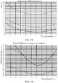
- FIG. 1 is a schematic diagram of influence of modulating driving amplitude
- FIG. 1A is a schematic diagram of an OSNR (Optical Signal Noise Ratio) tolerance curve.
- ---------- denotes the OSNR tolerance curve when the optical filter bandwidth is 75GHz (BER 1e-12).
- FIG. 1B is a schematic diagram of a dispersion tolerance curve in simulation, and in FIG.
- the curves of the OSNR tolerance and the back to back 2dB OSNR cost dispersion tolerance following the change of modulating the driving amplitude are shown in FIG. 1 .
- the OSNR tolerance and the 2dB OSNR cost dispersion tolerance remain stable at first, and then increase rapidly, but the increasing rate is slower than that at the decreasing of the driving amplitude; and when the driving amplitude increases to 1.5Vpi, compared with the Vpi, it brings that the OSNR cost is almost 2dB, which is much larger than the case of NRZ-DPSK.
- the change of the driving amplitude has relatively large influence on the NRZ-DQPSK performance, and when the driving amplitude is 1.1Vpi, although the dispersion tolerance is minimum, its OSNR performance is the best.
- the driving amplitude is 1.1Vpi, although the dispersion tolerance is minimum, its OSNR performance is the best.
- the NRZ-DQPSK system with rate of 40Gb/s a superior OSNR performance is more concerned, thus the best driving amplitude is taken as 1.1Vpi. Therefore, the stability of the driving amplitude has a large influence on the OSNR performance of the NRZ-DQPSK transmitter, and the driving amplitude needs to be controlled strictly.
- FIG. 2 is a block diagram of a structure of a feedback control apparatus of a DQPSK transmitter.
- the CW denotes the continuous spectrum light source of the unmodulated signal
- the driver I and the driver Q denote drivers of two upper and lower Mach-Zender modulators of the DQPSK modulator
- the Bias 1, Bias 2 and Bias 3 are the bias point 1, the bias point 2 and the bias point 3.
- the light emitted from the CW is modulated by the DQPSK modulator to generate a modulated optical signal to output, wherein, a part of the modulated optical signal is used to control the states of the modulator, the driver I and the driver Q.
- the disadvantage of the related art is that: since the DQPSK transmitter needs to control the three bias points of the modulator, the control circuit is relatively complicated already, then, if the driving amplitude is controlled by using the conventional method in which the pilot signal is added and by the time division multiplexing mode, the control circuit is very large, and adding the pilot signal might introduce a certain amount of OSNR cost.
- US2007/019968A1 discloses a method for adequately controlling the DC bias of each of the optical modulating sections of an optical modulator even while the optical modulator is operating in normal mode and even with a simple structure.
- WO2007/104022A2 discloses a method, which includes computer program products, implementing and using techniques for controlling three or more nested modulators in an optical signal application.
- the technical problem to be solved in the present invention is to provide an apparatus according to claim 1 and a method according to claim 7 for controlling driving amplitude of a differential quadrature phase shift keying transmitter, so as to simplify the complexity of the control circuit of the DQPSK transmitter. Further improvements and embodiments are provided in the dependent claims.
- an apparatus for controlling driving amplitude of a DQPSK transmitter which comprises: a first bias point, a second bias point, a third bias point, a driver I, a driver Q, and a DQPSK modulator for modulating an optical signal emitted by the CW, the apparatus also comprises:
- the driver I feedback control unit comprises:
- the driver Q feedback control unit comprises:
- the temperature compensation curve is obtained according to the driving amplitude of an output signal of the driver and the drain voltage of the MOSFET of the driver.
- the driver I feedback control unit comprises:
- driver Q feedback control unit comprises:
- Also provided is a method for controlling driving amplitude of a DQPSK transmitter which comprises:
- controlling the driving amplitude of the driver I according to the temperature change of the driver I comprises:
- the temperature compensation curve is obtained according to the driving amplitude of an output signal of the driver and the drain voltage of the MOSFET of the driver.
- controlling the driving amplitude of the driver I according to the temperature change of the driver I comprises:
- the beneficial effects of the present invention are as follows: in the implementation of the present invention, since the modulator feedback control unit is connected with the first bias point, the second bias point and the third bias point, the first bias point, the second bias point and the third bias point are controlled according to a part of the optical signal modulated by the DQPSK modulator; however, the part of the modulated optical signal is not used to control the states of the driver I of the driver Q any more; meanwhile, the driving amplitudes of the driver I and the driver Q are controlled according to the temperature changes of the driver I and the driver Q, rather than controlled by the modulator feedback control unit, so that the driver amplitude control circuit is separated from the feedback control of the DQPSK modulator, and the driving amplitude of the driver is controlled through the temperature change of the driver. Therefore, compared with the related art, the present invention can simplify the complexity of the control circuit of the DQPSK transmitter. Moreover, there is no need to add the pilot signal on the driving amplitude of the driver, thus no extra OSNR cost is created.
- embodiments of the present invention provide a new technique for monitoring and controlling the driving amplitude, to simplify multiple intercoupling control circuits of the DQPSK transmitter, and to get rid of the mode in which the original driving amplitude control needs to use the modulator to feed back, but some signals of the driver itself are only needed to act as the feedback signals to control the driving amplitude.
- the specific embodiments of the present invention will be illustrated in combination with the accompanying drawings.
- FIG. 3 is a structural diagram of an apparatus for controlling driving amplitude of a DQPSK transmitter.
- the apparatus comprises: the first bias point Bias1, the second bias point Bias2, the third bias point Bias3, the driver I, the driver Q, and the DQPSK modulator which modulates the optical signal emitted from the CW, and the apparatus also comprises:
- the modulator feedback control unit does not detach a part of the modulated optical signal to control the states of the driver I and the driver Q
- the driver amplitude control circuit is separated from the feedback control of the DQPSK modulator, and other feedback signals are used to control the driving amplitude, that is: the driving amplitude of the driver is controlled according to the temperature change of the driver.
- FIG. 4 is a schematic diagram of a driver feedback control in a direct compensation mode.
- the driver has three levels, and each level is considered as a MOSFET (Metal Oxide Semiconductor Field Effect Transistor); VD3 is a drain voltage of the third-level MOSFET, VD2 is a drain voltage of the second-level MOSFET, and VD1 is a drain voltage of the first-level MOSFET.
- MOSFET Metal Oxide Semiconductor Field Effect Transistor
- the DC-DC is a switching power supply converter
- Vin is an input voltage converted by the DC-DC power supply.
- the TEMP SENSOR is a temperature sensor.
- the VG is a gate voltage of the MOSFET.
- the DAC is a Digital to Analog Converter.
- the driving amplitude of this driver is related to the VD3, thus the temperature sensor can be used to detect the temperature of the driver, and then a temperature compensation algorithm is used to change the feedback network of DC-DC, thus changing the value of the VD3, so as to ensure the driving amplitude of the driver unchanged.
- the process is that: the temperature sensor firstly detects the temperature of the driver, and calculates an offset of the VD3 by using the temperature compensation algorithm, then the DAC feeds back the offset to the DC-DC, and then the DC-DC controls the output voltage so as to change the value of the VD3.
- the driver I and the driver Q can individually use the temperature control circuit to control the driving amplitude.
- the modulator feedback control unit can use any control mode which will not affect the driver control circuit.
- FIG. 5 is a schematic diagram of a temperature compensation curve in a direct compensation mode.
- EYE-AMP is the driving amplitude of the output signal of the driver
- C is the Celsius temperature
- VD is the drain voltage of the MOSFET of the driver.
- the temperature compensation curve can be used to change the feedback network of the DC-DC, that is, the temperature compensation curve can be obtained according to the driving amplitude of the output signal of the driver and the drain voltage of the MOSFET of the driver, so as to be used for temperature compensation.
- control for the driver I and/or the driver Q can be as follows.
- the driver I feedback control unit can comprise:
- the driver Q feedback control unit can comprise:
- FIG. 6 is a schematic diagram of a driver feedback control in an indirect compensation mode.
- the driver has three levels, wherein, the VD3 is the drain voltage of the third-level MOSFET, the VD2 is the drain voltage of the second-level MOSFET, and the VD1 is the drain voltage of the first-level MOSFET.
- the DC-DC is a switching power supply converter
- Vin is the input voltage converted by the DC-DC power supply.
- the Current Monitor is a current monitor.
- the VG is the gate voltage of the MOSFET.
- the DAC is a Digital to Analog Converter.
- the driving amplitude of the driver changes due to the influence of the temperature
- the current through the VD3 might change, so that whether the driving amplitude of the driver changes can be indirectly detected by monitoring the current of the VD3. If the current change is monitored, then the current of the VD3 can be corrected by changing the voltage of the VG3, to guarantee the current of the VD3 unchanged, thus the driving amplitude of the driver is controlled.
- the driver I and the driver Q can individually use the temperature control circuit to control the driving amplitude.
- the modulator feedback control unit can use any control mode which will not affect the driver control circuit.
- control for the driver I and/or the driver Q can be as follows.
- the driver I feedback control unit can comprise:
- the driver Q feedback control unit can comprise:
- the control mode of the direct compensation mode is simple, and the feedback control can be executed as long as the whole temperature range of the compensation curve of the driver is known.
- the control mode of the indirect compensation mode is relatively complicated, and the feedback control is executed which is required to use the current monitoring mode.
- the control accuracy of the indirect compensation mode is higher than that of the direct compensation mode, and the driving amplitude can be controlled by monitoring the tiny change in current.
- different control modes can be applied according to different application scenarios.
- the direct compensation and indirect compensation are taken for example to illustrate in the implementation, but in theory, other modes might be also used, as long as the driving amplitude of the driver can be controlled according to the temperature change of the driver; and the direct compensation and the indirect compensation are only used to teach those skilled in the art how to implement the present invention, which are not intended to user the two modes only, and in the implementation process, an appropriate mode might be determined in combination with the practical requirement.
- the embodiments of the present invention also provides a method for controlling the driving amplitude of the DQPSK transmitter. Since the principle of this method to solve the problem is similar to the apparatus for controlling the driving amplitude of the DQPSK transmitter, the implementation of this method can refer to the implementation of the apparatus and the repeated places are not repeated here.
- FIG. 7 is a diagram of an implementation process of a method for controlling driving amplitude of a DQPSK transmitter, and as shown in FIG. 7 , the following steps can be comprised when controlling the driving amplitude:
- controlling the driving amplitude of the driver I according to the temperature change of the driver I can comprise:
- controlling the driving amplitude of the driver Q according to the temperature change of the driver Q can comprise:
- the temperature compensation curve can be obtained according to the driving amplitude of the output signal of the driver and the drain voltage of the MOSFET of the driver.
- controlling the driving amplitude of the driver I according to the temperature change of the driver I can comprise:
- controlling the driving amplitude of the driver Q according to the temperature change of the driver Q can comprise:
- the modulator feedback control unit is used to control the voltages of the three bias points of the DQPSK modulator
- the driver feedback control unit is used to individually control the driving amplitude of the driver.
- the present invention can simplify the complexity of the control circuit of the DQPSK transmitter.
- the present invention does not need to add the pilot signal on the driving amplitude of the driver, thus no extra OSNR cost would be created.
Landscapes
- Physics & Mathematics (AREA)
- Electromagnetism (AREA)
- Engineering & Computer Science (AREA)
- Computer Networks & Wireless Communication (AREA)
- Signal Processing (AREA)
- Optics & Photonics (AREA)
- Optical Communication System (AREA)
- Optical Modulation, Optical Deflection, Nonlinear Optics, Optical Demodulation, Optical Logic Elements (AREA)
- Control Of Temperature (AREA)
Description
- The present invention relates to the communications equipment, and more particularly, to an apparatus and a method for controlling driving amplitude of a differential quadrature phase shift keying transmitter.
- A lot of new modulation techniques, such as DPSK (Differential Phase Shift Keying), DQPSK (Differential Quadrature Phase Shift Keying), and so on, are applied in the optical communication, and the DQPSK coding occupies an important position in the 40G optical communication system because it can reduce the requirements on rate, dispersion and PMD (polarization mode dispersion) of electrical devices. When a DQPSK transmitter modulates to generate a NRZ-DQPSK (Non-Return-to-Zero- DQPSK) signal by using an MZM (Mach-Zender Modulator), the effect due to the change of the driving amplitude is much bigger than the NRZ-DPSK.
-
FIG. 1 is a schematic diagram of influence of modulating driving amplitude, wherein,FIG. 1A is a schematic diagram of an OSNR (Optical Signal Noise Ratio) tolerance curve. InFIG. 1A , ― denotes the OSNR tolerance curve when the optical filter bandwidth is 37.5GHz (bit error rate (BER)=1e-4); - · - · denotes the OSNR tolerance curve when the optical filter bandwidth is 75GHz (BER=1e-4); and ---------- denotes the OSNR tolerance curve when the optical filter bandwidth is 75GHz (BER=1e-12).FIG. 1B is a schematic diagram of a dispersion tolerance curve in simulation, and inFIG. 1B , ― denotes the dispersion tolerance curve when the optical filter bandwidth is 37.5GHz (BER=1e-4); - · - · denotes the dispersion tolerance curve when the optical filter bandwidth is 75GHz (BER=1e-4); and ---------- denotes the dispersion tolerance curve when the optical filter bandwidth is 75GHz (BER=1e-12). In different optical filter bandwidths (37.5GHz and 75GHz), the curves of the OSNR tolerance and the back to back 2dB OSNR cost dispersion tolerance following the change of modulating the driving amplitude are shown inFIG. 1 . - It can be seen from
FIG. 1 that, when the driving amplitude is less than Vpi, in the two optical filter bandwidths (37.5GHz and 75GHz), with the decreasing of the driving amplitude, both the OSNR tolerance and the 2dB OSNR cost dispersion tolerance increase rapidly, and when the driving amplitude is reduced to 0.5Vpi, compared with the Vpi, it brings that the OSNR cost is more than 4dB, which is much larger than the case of NRZ-DPSK. When the driving amplitude is larger than Vpi, in the two optical filter bandwidths (37.5GHz and 75GHz), with the increasing of the driving amplitude, the OSNR tolerance and the 2dB OSNR cost dispersion tolerance remain stable at first, and then increase rapidly, but the increasing rate is slower than that at the decreasing of the driving amplitude; and when the driving amplitude increases to 1.5Vpi, compared with the Vpi, it brings that the OSNR cost is almost 2dB, which is much larger than the case of NRZ-DPSK. - The change of the driving amplitude has relatively large influence on the NRZ-DQPSK performance, and when the driving amplitude is 1.1Vpi, although the dispersion tolerance is minimum, its OSNR performance is the best. For the NRZ-DQPSK system with rate of 40Gb/s, a superior OSNR performance is more concerned, thus the best driving amplitude is taken as 1.1Vpi. Therefore, the stability of the driving amplitude has a large influence on the OSNR performance of the NRZ-DQPSK transmitter, and the driving amplitude needs to be controlled strictly.
-
FIG. 2 is a block diagram of a structure of a feedback control apparatus of a DQPSK transmitter. InFIG. 2 , the CW denotes the continuous spectrum light source of the unmodulated signal, the driver I and the driver Q denote drivers of two upper and lower Mach-Zender modulators of the DQPSK modulator, theBias 1, Bias 2 and Bias 3 are thebias point 1, thebias point 2 and the bias point 3. As shown inFIG. 2 , the light emitted from the CW is modulated by the DQPSK modulator to generate a modulated optical signal to output, wherein, a part of the modulated optical signal is used to control the states of the modulator, the driver I and the driver Q. - The disadvantage of the related art is that: since the DQPSK transmitter needs to control the three bias points of the modulator, the control circuit is relatively complicated already, then, if the driving amplitude is controlled by using the conventional method in which the pilot signal is added and by the time division multiplexing mode, the control circuit is very large, and adding the pilot signal might introduce a certain amount of OSNR cost.
- The document
US2007/019968A1 discloses a method for adequately controlling the DC bias of each of the optical modulating sections of an optical modulator even while the optical modulator is operating in normal mode and even with a simple structure. - The document
US2004/247225A1 discloses optical modulators with reduced temperature dependence on bias control. A set of bias electrodes is arranged relative to a set of RF electrodes in a manner which results in the operating point of the device remaining relatively constant as a function of temperature. - The document
WO2007/104022A2 discloses a method, which includes computer program products, implementing and using techniques for controlling three or more nested modulators in an optical signal application. - The technical problem to be solved in the present invention is to provide an apparatus according to
claim 1 and a method according to claim 7 for controlling driving amplitude of a differential quadrature phase shift keying transmitter, so as to simplify the complexity of the control circuit of the DQPSK transmitter. Further improvements and embodiments are provided in the dependent claims. - Also provided is an apparatus for controlling driving amplitude of a DQPSK transmitter, which comprises: a first bias point, a second bias point, a third bias point, a driver I, a driver Q, and a DQPSK modulator for modulating an optical signal emitted by the CW, the apparatus also comprises:
- a modulator feedback control unit, which is connected with the first bias point, the second bias point and the third bias point, and is configured to control the first bias point, the second bias point and the third bias point according to a part of the optical signal modulated by the DQPSK modulator;
- a driver I feedback control unit, which is connected with the driver I and is configured to control the driving amplitude of the driver I according to temperature change of the driver I; and
- a driver Q feedback control unit, which is connected with the driver Q and is configured to control the driving amplitude of the driver Q according to temperature change of the driver Q.
- Preferably, the driver I feedback control unit comprises:
- a first temperature sensor, which is connected with the driver I and is configured to detect the temperature change of the driver I; and
- a first direct compensation module, which is configured to compensate in light of a temperature compensation curve and according to the temperature change of the driver I, and after obtaining an offset of a drain voltage of a third-level metal oxide semiconductor field effect transistor (MOSFET) of the driver I, feed back the offset to a switching power supply converter connected with the driver I, so as to control change of the drain voltage of the third-level MOSFET of the driver I.
- Preferably, the driver Q feedback control unit comprises:
- a second temperature sensor, which is connected with the driver Q and is configured to detect the temperature change of the driver Q; and
- a second direct compensation module, which is configured to compensate in light of a temperature compensation curve and according to the temperature change of the driver Q, and after obtaining an offset of a drain voltage of a third-level MOSFET of the driver Q, feed back the offset to a switching power supply converter connected with the driver Q, so as to control change of the drain voltage of the third-level MOSFET of the driver Q.
- Preferably, the temperature compensation curve is obtained according to the driving amplitude of an output signal of the driver and the drain voltage of the MOSFET of the driver.
- Preferably, the driver I feedback control unit comprises:
- a first current monitoring module, which is connected with a drain voltage of a third-level MOSFET of the driver I and is configured to monitor current change of the drain voltage of the third-level MOSFET of the driver I; and
- a first indirect compensation module, which is configured to control voltage change of a gate voltage of the third-level MOSFET according to the current change of the drain voltage of the third-level MOSFET of the driver I, and control the current change of the drain voltage of the third-level MOSFET by controlling the voltage change of the gate voltage of the third-level MOSFET.
- Preferably the driver Q feedback control unit comprises:
- a second current monitoring module, which is connected with a drain voltage of a third-level MOSFET of the driver Q and is configured to monitor current change of the drain voltage of the third-level MOSFET of the driver Q; and
- a second indirect compensation module, which is configured to control voltage change of a gate voltage of the third-level MOSFET according to the current change of the drain voltage of the third-level MOSFET of the driver Q, and control the current change of the drain voltage of the third-level MOSFET by controlling the voltage change of the gate voltage of the third-level MOSFET.
- Also provided is a method for controlling driving amplitude of a DQPSK transmitter, which comprises:
- modulating, by a DQPSK modulator, an optical signal emitted from a CW;
- connecting a modulator feedback control unit with a first bias point, a second bias point and a third bias point, and controlling, by the modulator feedback control unit, the first bias point, the second bias point and the third bias point according to a part of the optical signal modulated by the DQPSK modulator;
- controlling the driving amplitude of a driver I according to temperature change of the driver I;
- controlling the driving amplitude of a driver Q according to temperature change of the driver Q.
- Preferably, controlling the driving amplitude of the driver I according to the temperature change of the driver I comprises:
- detecting the temperature change of the driver I;
- compensating in light of a temperature compensation curve and according to the temperature change of the driver I, and after obtaining an offset of a drain voltage of a third-level metal oxide semiconductor field effect transistor (MOSFET) of the driver I, feeding back the offset to a switching power supply converter connected with the driver I, so as to control change of the drain voltage of the third-level MOSFET of the driver I;
- and/or,
- controlling the driving amplitude of the driver Q according to the temperature change of the driver Q comprises:
- detecting the temperature change of the driver Q;
- compensating in light of a temperature compensation curve and according to the temperature change of the driver Q, and after obtaining an offset of a drain voltage of a third-level MOSFET of the driver Q, feeding back the offset to a switching power supply converter connected with the driver Q, so as to control change of the drain voltage of the third-level MOSFET of the driver Q.
- Preferably, the temperature compensation curve is obtained according to the driving amplitude of an output signal of the driver and the drain voltage of the MOSFET of the driver.
- Preferably, controlling the driving amplitude of the driver I according to the temperature change of the driver I comprises:
- monitoring current change of a drain voltage of a third-level MOSFET of the driver I;
- controlling voltage change of a gate voltage of the third-level MOSFET according to the current change of the drain voltage of the third-level MOSFET of the driver I, and controlling the current change of the drain voltage of the third-level MOSFET by controlling the voltage change of the gate voltage of the third-level MOSFET;
- and/or,
- controlling the driving amplitude of the driver Q according to the temperature change of the driver Q comprises:
- monitoring current change of a drain voltage of a third-level MOSFET of the driver Q;
- controlling voltage change of a gate voltage of the third-level MOSFET according to the current change of the drain voltage of the third-level MOSFET of the driver Q, and controlling the current change of the drain voltage of the third-level MOSFET by controlling the voltage change of the gate voltage of the third-level MOSFET.
- The beneficial effects of the present invention are as follows:
in the implementation of the present invention, since the modulator feedback control unit is connected with the first bias point, the second bias point and the third bias point, the first bias point, the second bias point and the third bias point are controlled according to a part of the optical signal modulated by the DQPSK modulator; however, the part of the modulated optical signal is not used to control the states of the driver I of the driver Q any more; meanwhile, the driving amplitudes of the driver I and the driver Q are controlled according to the temperature changes of the driver I and the driver Q, rather than controlled by the modulator feedback control unit, so that the driver amplitude control circuit is separated from the feedback control of the DQPSK modulator, and the driving amplitude of the driver is controlled through the temperature change of the driver. Therefore, compared with the related art, the present invention can simplify the complexity of the control circuit of the DQPSK transmitter. Moreover, there is no need to add the pilot signal on the driving amplitude of the driver, thus no extra OSNR cost is created. -
-
FIG. 1 is a schematic diagram of influence of modulating driving amplitude in the related art, wherein:FIG. 1A is a schematic diagram of an OSNR tolerance curve, andFIG. 1B is a schematic diagram of a dispersion tolerance curve in simulation; -
FIG. 2 is a block diagram of a structure of a feedback control apparatus of a DQPSK transmitter in the related art; -
FIG. 3 is a structural diagram of an apparatus for controlling driving amplitude of a DQPSK transmitter in accordance with an embodiment of the present invention; -
FIG. 4 is a schematic diagram of a driver feedback control in a direct compensation mode in accordance with an embodiment of the present invention; -
FIG. 5 is a schematic diagram of a temperature compensation curve in a direct compensation mode in accordance with an embodiment of the present invention; -
FIG. 6 is a schematic diagram of a driver feedback control in an indirect compensation mode in accordance with an embodiment of the present invention; -
FIG. 7 is a flow chart of a method for controlling driving amplitude of a DQPSK transmitter in accordance with an embodiment of the present invention. - Since a DQPSK transmitter needs to control three bias points of a modulator, the control circuit is relatively complicated already, then, if the driving amplitude is controlled by using the conventional method in which the pilot signal is added and by the time division multiplexing mode, the control circuit is very large, and at the same time adding the pilot signal might introduce a certain amount of OSNR cost. Therefore, embodiments of the present invention provide a new technique for monitoring and controlling the driving amplitude, to simplify multiple intercoupling control circuits of the DQPSK transmitter, and to get rid of the mode in which the original driving amplitude control needs to use the modulator to feed back, but some signals of the driver itself are only needed to act as the feedback signals to control the driving amplitude. In the following, the specific embodiments of the present invention will be illustrated in combination with the accompanying drawings.
-
FIG. 3 is a structural diagram of an apparatus for controlling driving amplitude of a DQPSK transmitter. As shown inFIG. 3 , the apparatus comprises: the first bias point Bias1, the second bias point Bias2, the third bias point Bias3, the driver I, the driver Q, and the DQPSK modulator which modulates the optical signal emitted from the CW, and the apparatus also comprises: - a modulator feedback control unit, which is connected with the first bias point, the second bias point and the third bias point and is used to control the first bias point, the second bias point and the third bias point according to a part of the optical signal modulated by the DQPSK modulator; wherein, the part of the optical signal is about 10%;
- the driver I feedback control unit, which is connected with the driver I and is used to control the driving amplitude of the driver I according to the temperature change of the driver I;
- the driver Q feedback control unit, which is connected with the driver Q and is used to control the driving amplitude of the driver Q according to the temperature change of the driver Q.
- From the aforementioned scheme, it can be seen that the modulator feedback control unit does not detach a part of the modulated optical signal to control the states of the driver I and the driver Q, the driver amplitude control circuit is separated from the feedback control of the DQPSK modulator, and other feedback signals are used to control the driving amplitude, that is: the driving amplitude of the driver is controlled according to the temperature change of the driver.
- In the implementation, considering that the existing high-speed drivers of which the signal bandwidth is up to 30-40GHz almost use a multi-polar FET (field effect transistor) amplifier serial structure, the amplifier gain will change with the change of the temperature, which will lead to the change of the driving amplitude. Therefore, different embodiments of controlling the driving amplitude by using the temperature are provided in the following.
-
FIG. 4 is a schematic diagram of a driver feedback control in a direct compensation mode. InFIG. 4 , the driver has three levels, and each level is considered as a MOSFET (Metal Oxide Semiconductor Field Effect Transistor); VD3 is a drain voltage of the third-level MOSFET, VD2 is a drain voltage of the second-level MOSFET, and VD1 is a drain voltage of the first-level MOSFET. - The DC-DC is a switching power supply converter, Vin is an input voltage converted by the DC-DC power supply.
- The TEMP SENSOR is a temperature sensor.
- The VG is a gate voltage of the MOSFET.
- The DAC is a Digital to Analog Converter.
- As shown in
FIG. 4 , in the direct compensation mode, the driving amplitude of this driver is related to the VD3, thus the temperature sensor can be used to detect the temperature of the driver, and then a temperature compensation algorithm is used to change the feedback network of DC-DC, thus changing the value of the VD3, so as to ensure the driving amplitude of the driver unchanged. Specifically, the process is that: the temperature sensor firstly detects the temperature of the driver, and calculates an offset of the VD3 by using the temperature compensation algorithm, then the DAC feeds back the offset to the DC-DC, and then the DC-DC controls the output voltage so as to change the value of the VD3. The driver I and the driver Q can individually use the temperature control circuit to control the driving amplitude. The modulator feedback control unit can use any control mode which will not affect the driver control circuit. -
FIG. 5 is a schematic diagram of a temperature compensation curve in a direct compensation mode. InFIG. 5 , EYE-AMP is the driving amplitude of the output signal of the driver, C is the Celsius temperature, and VD is the drain voltage of the MOSFET of the driver. As shown inFIG. 5 , the temperature compensation curve can be used to change the feedback network of the DC-DC, that is, the temperature compensation curve can be obtained according to the driving amplitude of the output signal of the driver and the drain voltage of the MOSFET of the driver, so as to be used for temperature compensation. - From the aforementioned embodiment, it can be seen that in the specific implementation, the control for the driver I and/or the driver Q can be as follows.
- The driver I feedback control unit can comprise:
- a first temperature sensor, which is connected with the driver I and is used to detect the temperature change of the driver I;
- a first direct compensation module, which is used to compensate in light of the temperature compensation curve and according to the temperature change of the driver I to obtain the offset of the VD3, and then feed back the offset of the VD3 to the switching power supply converter DC-DC, so as to control the change of the drain voltage VD3 of the third-level MOSFET.
- The driver Q feedback control unit can comprise:
- a second temperature sensor, which is connected with the driver Q and is used to detect the temperature change of the driver Q;
- a second direct compensation module, which is used to compensate in light of the temperature compensation curve and according to the temperature change of the driver Q, and then feed back to the switching power supply converter DC-DC, so as to control the change of the drain voltage VD3 of the third-level MOSFET.
-
FIG. 6 is a schematic diagram of a driver feedback control in an indirect compensation mode. InFIG. 6 , the driver has three levels, wherein, the VD3 is the drain voltage of the third-level MOSFET, the VD2 is the drain voltage of the second-level MOSFET, and the VD1 is the drain voltage of the first-level MOSFET. - The DC-DC is a switching power supply converter, the Vin is the input voltage converted by the DC-DC power supply.
- The Current Monitor is a current monitor.
- The VG is the gate voltage of the MOSFET.
- The DAC is a Digital to Analog Converter.
- As shown in
FIG. 6 , in the indirect compensation mode, if the driving amplitude of the driver changes due to the influence of the temperature, then the current through the VD3 might change, so that whether the driving amplitude of the driver changes can be indirectly detected by monitoring the current of the VD3. If the current change is monitored, then the current of the VD3 can be corrected by changing the voltage of the VG3, to guarantee the current of the VD3 unchanged, thus the driving amplitude of the driver is controlled. The driver I and the driver Q can individually use the temperature control circuit to control the driving amplitude. The modulator feedback control unit can use any control mode which will not affect the driver control circuit. - From the aforementioned embodiment, in the specific implementation it can be seen that, the control for the driver I and/or the driver Q can be as follows.
- The driver I feedback control unit can comprise:
- a first current monitoring module, which is connected with the VD3 of the driver I and is used to monitor the current change of the VD3 of the driver I;
- a first indirect compensation module, which is used to control the voltage change of the gate voltage VG3 of the third-level MOSFET according to the current change of the VD3 of the driver I, and control the current change of the drain voltage VD3 of the third-level MOSFET by controlling the voltage change of the VG3.
- The driver Q feedback control unit can comprise:
- a second current monitoring module, which is connected with the VD3 of the driver Q and is used to monitor the current change of the VD3 of the driver Q;
- a second indirect compensation module, which is used to control the voltage change of the VG3 according to the current change of the VD3 of the driver Q, and control the current change of the drain voltage VD3 of the third-level MOSFET by controlling the voltage change of the VG3.
- In the aforementioned embodiment, the control mode of the direct compensation mode is simple, and the feedback control can be executed as long as the whole temperature range of the compensation curve of the driver is known. The control mode of the indirect compensation mode is relatively complicated, and the feedback control is executed which is required to use the current monitoring mode. However, the control accuracy of the indirect compensation mode is higher than that of the direct compensation mode, and the driving amplitude can be controlled by monitoring the tiny change in current. In the specific implementation, different control modes can be applied according to different application scenarios.
- The direct compensation and indirect compensation are taken for example to illustrate in the implementation, but in theory, other modes might be also used, as long as the driving amplitude of the driver can be controlled according to the temperature change of the driver; and the direct compensation and the indirect compensation are only used to teach those skilled in the art how to implement the present invention, which are not intended to user the two modes only, and in the implementation process, an appropriate mode might be determined in combination with the practical requirement.
- Based on the same inventive concept, the embodiments of the present invention also provides a method for controlling the driving amplitude of the DQPSK transmitter. Since the principle of this method to solve the problem is similar to the apparatus for controlling the driving amplitude of the DQPSK transmitter, the implementation of this method can refer to the implementation of the apparatus and the repeated places are not repeated here.
-
FIG. 7 is a diagram of an implementation process of a method for controlling driving amplitude of a DQPSK transmitter, and as shown inFIG. 7 , the following steps can be comprised when controlling the driving amplitude: - in
step 701, the DQPSK modulator modulates the optical signal emitted from the CW; - in
step 702, the modulator feedback control unit is connected with the first bias point, the second bias point and the third bias point, and controls the first bias point, the second bias point and the third bias point according to a part of the optical signal modulated by the DQPSK modulator; - in
step 703, the driving amplitude of the driver I is controlled according to the temperature change of the driver I; - in
step 704, the driving amplitude of the driver Q is controlled according to the temperature change of the driver Q. - In the implementation, there is no necessary timing requirement among
steps - In the implementation, controlling the driving amplitude of the driver I according to the temperature change of the driver I can comprise:
- detecting the temperature change of the driver I;
- compensating in light of the temperature compensation curve and according to the temperature change of the driver I, and then feeding back to the switching power supply converter DC-DC, so as to control the change of the drain voltage VD3 of the third-level MOSFET.
- In the implementation, controlling the driving amplitude of the driver Q according to the temperature change of the driver Q can comprise:
- detecting the temperature change of the driver Q;
- compensating in light of the temperature compensation curve and according to the temperature change of the driver Q, and then feeding back to the switching power supply converter DC-DC, so as to control the change of the drain voltage VD3 of the third-level MOSFET.
- In the implementation, the temperature compensation curve can be obtained according to the driving amplitude of the output signal of the driver and the drain voltage of the MOSFET of the driver.
- In the implementation, controlling the driving amplitude of the driver I according to the temperature change of the driver I can comprise:
- monitoring the current change of the VD3 of the driver I;
- controlling the voltage change of the gate voltage VG3 of the third-level MOSFET according to the current change of the VD3 of the driver I, and controlling the current change of the drain voltage VD3 of the third-level MOSFET by controlling the voltage change of the VG3.
- In the implementation, controlling the driving amplitude of the driver Q according to the temperature change of the driver Q can comprise:
- monitoring the current change of the VD3 of the driver Q;
- controlling the voltage change of the VG3 according to the current change of the VD3 of the driver Q, and controlling the current change of the drain voltage VD3 of the third-level MOSFET by controlling the voltage change of the VG3.
- From the aforementioned embodiment, it can be seen that, in the technical solution provided in the embodiments of the present invention, since the modulator feedback control unit is used to control the voltages of the three bias points of the DQPSK modulator, the driver feedback control unit is used to individually control the driving amplitude of the driver. Compared with the related art, the present invention can simplify the complexity of the control circuit of the DQPSK transmitter. Moreover, the present invention does not need to add the pilot signal on the driving amplitude of the driver, thus no extra OSNR cost would be created.
- Although the preferred embodiments of the present invention are described, once those skilled in the art acquire the basic creative concept, they can make additional changes and modifications on these embodiments. Therefore, the appended claims intend to include the preferred embodiments as well as all changes and modifications that fall into the scope of the present invention.
- Obviously, those skilled in the art can make various modifications and variations on the present invention, without departing from the scope of the present invention. Thus, if these modifications and variations of the present invention fall into the scope of the claims of the present invention and its equivalent technologies, then the present invention also intends to include these modifications and variations into.
Claims (10)
- An apparatus for controlling driving amplitude of a differential quadrature phase shift keying, DQPSK, transmitter, characterized by comprising: a first bias point, a second bias point, a third bias point, a driver I, a driver Q, and a DQPSK modulator for modulating an optical signal emitted by a continuous wave light source, CW, of an unmodulated signal, wherein, the apparatus further comprises:
a modulator feedback control unit, a driver I feedback control unit and a driver Q feedback control unit; wherein,the modulator feedback control unit is connected with the first bias point, the second bias point and the third bias point, and is configured to control the voltages of the first bias point, the voltages of the second bias point and the voltages of the third bias point according to a part of the optical signal modulated by the DQPSK modulator;the driver I feedback control unit is connected with the driver I and is configured to control the driving amplitude of the driver I according to temperature change of the driver I; andthe driver Q feedback control unit is connected with the driver Q and is configured to control the driving amplitude of the driver Q according to temperature change of the driver Q. - The apparatus of claim 1, wherein, the driver I feedback control unit comprises a first temperature sensor and a first direct compensation module; wherein,
the first temperature sensor is connected with the driver I and is configured to detect the temperature change of the driver I; and
the first direct compensation module is configured to compensate in light of a temperature compensation curve and according to the temperature change of the driver I, and after obtaining an offset of a drain voltage of a third-level metal oxide semiconductor field effect transistor, MOSFET, of the driver I, feed back the offset to a switching power supply converter connected with the driver I, so as to control change of the drain voltage of the third-level MOSFET of the driver I. - The apparatus of claim 1, wherein, the driver Q feedback control unit comprises a second temperature sensor and a second direct compensation module; wherein,
the second temperature sensor is connected with the driver Q and is configured to detect the temperature change of the driver Q; and
the second direct compensation module is configured to compensate in light of a temperature compensation curve and according to the temperature change of the driver Q, and after obtaining an offset of a drain voltage of a third-level MOSFET of the driver Q, feed back the offset to a switching power supply converter connected with the driver Q, so as to control change of the drain voltage of the third-level MOSFET of the driver Q. - The apparatus of claim 2 or 3, wherein, the temperature compensation curve is obtained according to the driving amplitude of an output signal of the driver and the drain voltage of the MOSFET of the driver.
- The apparatus of claim 1, wherein, the driver I feedback control unit comprises a first current monitoring module and a first indirect compensation module; wherein,
the first current monitoring module is connected with a drain voltage of a third-level MOSFET of the driver I and is configured to monitor current change of the drain voltage of the third-level MOSFET of the driver I; and
the first indirect compensation module is configured to control voltage change of a gate voltage of the third-level MOSFET according to the current change of the drain voltage of the third-level MOSFET of the driver I, and control the current change of the drain voltage of the third-level MOSFET by controlling the voltage change of the gate voltage of the third-level MOSFET. - The apparatus of claim 1, wherein, the driver Q feedback control unit comprises a second current monitoring module and a second indirect compensation module; wherein,
the second current monitoring module is connected with a drain voltage of a third-level MOSFET of the driver Q and is configured to monitor current change of the drain voltage of the third-level MOSFET of the driver Q; and
the second indirect compensation module is configured to control voltage change of a gate voltage of the third-level MOSFET according to the current change of the drain voltage of the third-level MOSFET of the driver Q, and control the current change of the drain voltage of the third-level MOSFET by controlling the voltage change of the gate voltage of the third-level MOSFET. - A method for controlling driving amplitude of a differential quadrature phase shift keying, DQPSK, transmitter, characterized by comprising:Modulating (701), by a DQPSK modulator, an optical signal emitted from a CW;connecting a modulator feedback control unit with a first bias point, a second bias point and a third bias point of said DQPSK modulator, and controlling, by the modulator feedback control unit, the voltages of the first bias point, the voltages of the second bias point and the voltages of the third bias point according to a part of the optical signal modulated by the DQPSK modulator (702);controlling the driving amplitude of a driver I according to temperature change of the driver I (703);controlling the driving amplitude of a driver Q according to temperature change of the driver Q (704).
- The method of claim 7, wherein, controlling the driving amplitude of the driver I according to the temperature change of the driver I comprises:detecting the temperature change of the driver I;compensating in light of a temperature compensation curve and according to the temperature change of the driver I, and after obtaining an offset of a drain voltage of a third-level metal oxide semiconductor field effect transistor, MOSFET, of the driver I, feeding back the offset to a switching power supply converter connected with the driver I, so as to control change of the drain voltage of the third-level MOSFET of the driver I;and/or,controlling the driving amplitude of the driver Q according to the temperature change of the driver Q comprises:detecting the temperature change of the driver Q;compensating in light of a temperature compensation curve and according to the temperature change of the driver Q, and after obtaining an offset of a drain voltage of a third-level MOSFET of the driver Q, feeding back the offset to a switching power supply converter connected with the driver Q, so as to control change of the drain voltage of the third-level MOSFET of the driver Q.
- The method of claim 8, wherein, the temperature compensation curve is obtained according to the driving amplitude of an output signal of the driver and the drain voltage of the MOSFET of the driver.
- The method of claim 7, wherein, controlling the driving amplitude of the driver I according to the temperature change of the driver I comprises:monitoring current change of a drain voltage of a third-level MOSFET of the driver I;controlling voltage change of a gate voltage of the third-level MOSFET according to the current change of the drain voltage of the third-level MOSFET of the driver I, and controlling the current change of the drain voltage of the third-level MOSFET by controlling the voltage change of the gate voltage of the third-level MOSFET;and/or,controlling the driving amplitude of the driver Q according to the temperature change of the driver Q comprises:monitoring current change of a drain voltage of a third-level MOSFET of the driver Q;controlling voltage change of a gate voltage of the third-level MOSFET according to the current change of the drain voltage of the third-level MOSFET of the driver Q, and controlling the current change of the drain voltage of the third-level MOSFET by controlling the voltage change of the gate voltage of the third-level MOSFET.
Applications Claiming Priority (2)
| Application Number | Priority Date | Filing Date | Title |
|---|---|---|---|
| CN2009101783239A CN101674138B (en) | 2009-10-16 | 2009-10-16 | Driving magnitude control device of differential quadrature phase shift keying transmitter and method |
| PCT/CN2010/074513 WO2010145585A1 (en) | 2009-10-16 | 2010-06-25 | Apparatus and method for control the driving amplitude of differential quadrature phase shift keying transmitter |
Publications (3)
| Publication Number | Publication Date |
|---|---|
| EP2490352A1 EP2490352A1 (en) | 2012-08-22 |
| EP2490352A4 EP2490352A4 (en) | 2016-06-29 |
| EP2490352B1 true EP2490352B1 (en) | 2018-10-17 |
Family
ID=42021158
Family Applications (1)
| Application Number | Title | Priority Date | Filing Date |
|---|---|---|---|
| EP10788981.8A Active EP2490352B1 (en) | 2009-10-16 | 2010-06-25 | Apparatus and method for control the driving amplitude of differential quadrature phase shift keying transmitter |
Country Status (6)
| Country | Link |
|---|---|
| US (1) | US20120207483A1 (en) |
| EP (1) | EP2490352B1 (en) |
| JP (1) | JP2013507855A (en) |
| KR (1) | KR20120083467A (en) |
| CN (1) | CN101674138B (en) |
| WO (1) | WO2010145585A1 (en) |
Families Citing this family (10)
| Publication number | Priority date | Publication date | Assignee | Title |
|---|---|---|---|---|
| CN101674138B (en) * | 2009-10-16 | 2013-07-03 | 中兴通讯股份有限公司 | Driving magnitude control device of differential quadrature phase shift keying transmitter and method |
| CN102340468B (en) * | 2010-07-14 | 2015-08-12 | 中兴通讯股份有限公司 | The control method of drive signal amplitude and device, DQPSK transmitter system |
| CN102055406B (en) * | 2010-10-22 | 2014-08-13 | 中兴通讯股份有限公司 | Method and device for processing time sequence difference of driver |
| US9344194B2 (en) * | 2013-02-21 | 2016-05-17 | Fujitsu Limited | System and method for monitoring and control of an optical modulator for an M-QAM transmitter |
| CN104485997B (en) * | 2014-12-09 | 2017-04-12 | 华中科技大学 | Control system and method of bias voltage of IQ optical modulator |
| JP6601212B2 (en) * | 2015-12-24 | 2019-11-06 | 住友電気工業株式会社 | Optical transmitter |
| JP2017116746A (en) * | 2015-12-24 | 2017-06-29 | 富士通株式会社 | Optical transmitter and control method |
| US10861565B2 (en) * | 2018-12-31 | 2020-12-08 | Micron Technology, Inc. | Functional signal line overdrive |
| WO2022137517A1 (en) * | 2020-12-25 | 2022-06-30 | Nec Corporation | Optical transmitter and method of transmitting an optical signal |
| JP2024058965A (en) * | 2022-10-17 | 2024-04-30 | 日本電気株式会社 | Method and program for controlling transmitter and nested modulator in optical communication system |
Family Cites Families (16)
| Publication number | Priority date | Publication date | Assignee | Title |
|---|---|---|---|---|
| WO1994029962A1 (en) * | 1993-06-08 | 1994-12-22 | National Semiconductor Corporation | Cmos btl compatible bus and transmission line driver |
| JP3736953B2 (en) * | 1997-10-20 | 2006-01-18 | 富士通株式会社 | Electroabsorption optical modulator drive circuit and optical transmitter using the same |
| US6922045B2 (en) * | 2002-02-13 | 2005-07-26 | Primarion, Inc. | Current driver and method of precisely controlling output current |
| JP4083657B2 (en) * | 2003-03-28 | 2008-04-30 | 住友大阪セメント株式会社 | Bias control method and apparatus for optical modulator |
| US6978056B2 (en) * | 2003-06-04 | 2005-12-20 | Covega, Inc. | Waveguide modulators having bias control with reduced temperature dependence |
| JP4527993B2 (en) * | 2004-01-28 | 2010-08-18 | 日本放送協会 | Light modulation apparatus and light modulation method |
| DE602005005697T2 (en) * | 2005-11-25 | 2009-04-30 | Alcatel Lucent | Fiber optic transmission system, transmitter and receiver for DQPSK modulated signals and associated stabilization method |
| JP4781094B2 (en) * | 2005-11-30 | 2011-09-28 | 富士通株式会社 | Optical transmitter |
| US20070212075A1 (en) * | 2006-03-09 | 2007-09-13 | Yy Labs, Inc. | Dual-parallel-mz modulator bias control |
| CN101043269B (en) * | 2006-03-22 | 2011-01-05 | 富士通株式会社 | I-Q Quadrature Modulation Transmitter and Its Device and Method for Monitoring Phase Offset Between I-Q Channels |
| JP5405716B2 (en) * | 2006-09-29 | 2014-02-05 | 富士通株式会社 | Optical transmitter |
| US7733193B2 (en) * | 2007-11-01 | 2010-06-08 | Ciena Corporation | Systems and methods for DQPSK modulator control using selectively inserted dither tone |
| CN101276067A (en) * | 2008-05-05 | 2008-10-01 | 中兴通讯股份有限公司 | Dynamic control method and device for lithium niobate modulator |
| CN101453271A (en) * | 2008-09-03 | 2009-06-10 | 沈红 | Fast burst light transmitting method |
| JP5169710B2 (en) * | 2008-10-10 | 2013-03-27 | 富士通株式会社 | Optical receiver and dispersion compensation sequence control method |
| CN101674138B (en) * | 2009-10-16 | 2013-07-03 | 中兴通讯股份有限公司 | Driving magnitude control device of differential quadrature phase shift keying transmitter and method |
-
2009
- 2009-10-16 CN CN2009101783239A patent/CN101674138B/en active Active
-
2010
- 2010-06-25 WO PCT/CN2010/074513 patent/WO2010145585A1/en not_active Ceased
- 2010-06-25 US US13/501,595 patent/US20120207483A1/en not_active Abandoned
- 2010-06-25 JP JP2012533464A patent/JP2013507855A/en active Pending
- 2010-06-25 KR KR1020127012604A patent/KR20120083467A/en not_active Ceased
- 2010-06-25 EP EP10788981.8A patent/EP2490352B1/en active Active
Non-Patent Citations (1)
| Title |
|---|
| None * |
Also Published As
| Publication number | Publication date |
|---|---|
| EP2490352A1 (en) | 2012-08-22 |
| JP2013507855A (en) | 2013-03-04 |
| WO2010145585A1 (en) | 2010-12-23 |
| EP2490352A4 (en) | 2016-06-29 |
| US20120207483A1 (en) | 2012-08-16 |
| CN101674138A (en) | 2010-03-17 |
| KR20120083467A (en) | 2012-07-25 |
| CN101674138B (en) | 2013-07-03 |
Similar Documents
| Publication | Publication Date | Title |
|---|---|---|
| EP2490352A1 (en) | Apparatus and method for control the driving amplitude of differential quadrature phase shift keying transmitter | |
| US7773283B2 (en) | Optical modulation device and optical modulation method | |
| US9244328B2 (en) | Optical modulator and optical modulation control method | |
| US8098998B2 (en) | Optical transmitter | |
| EP2530855B1 (en) | Optical transmitter, control method for the same, and optical transmission system | |
| EP1906564A1 (en) | Optical transmitter | |
| US9853736B2 (en) | Optical transmitter and bias control method for optical modulator | |
| JP6217152B2 (en) | Optical transmitter and method for controlling optical transmitter | |
| US8693887B2 (en) | Optical transmitter and optical transmission system | |
| US20090324252A1 (en) | Optical Transmitter | |
| Tatsumi et al. | A compact low-power 224-Gb/s DP-16QAM modulator module with InP-based modulator and linear driver ICs | |
| JP5811531B2 (en) | Optical transmitter, optical communication system, and optical transmission method | |
| US6542280B2 (en) | Return-to-zero optical modulator with configurable pulse width | |
| CN112005159B (en) | Light modulator | |
| CN215732674U (en) | Laser driver and chip | |
| WO2006048944A1 (en) | Optical transmitter and optical communication system | |
| CN103391138B (en) | For the fast initialization numeral automatic optical power control circuit of laser driver | |
| HK1171290B (en) | Apparatus and method for control the driving amplitude of differential quadrature phase shift keying transmitter | |
| HK1171290A (en) | Apparatus and method for control the driving amplitude of differential quadrature phase shift keying transmitter | |
| US7630651B2 (en) | Method and apparatus for controlling bias point of optical transmitter | |
| US7257332B2 (en) | Optical transmitter and its control method | |
| US20120082467A1 (en) | Optical transmitter, optical transmission device, and method of controlling optical transmitter | |
| JPWO2014097503A1 (en) | Optical modulator, optical transmitter, optical transmission / reception system, and optical modulator control method | |
| JP4884338B2 (en) | Optical modulator driver adjustment device and adjustment method | |
| JP2017125867A (en) | Light transmitter, and source voltage control method |
Legal Events
| Date | Code | Title | Description |
|---|---|---|---|
| PUAI | Public reference made under article 153(3) epc to a published international application that has entered the european phase |
Free format text: ORIGINAL CODE: 0009012 |
|
| 17P | Request for examination filed |
Effective date: 20120322 |
|
| AK | Designated contracting states |
Kind code of ref document: A1 Designated state(s): AL AT BE BG CH CY CZ DE DK EE ES FI FR GB GR HR HU IE IS IT LI LT LU LV MC MK MT NL NO PL PT RO SE SI SK SM TR |
|
| DAX | Request for extension of the european patent (deleted) | ||
| REG | Reference to a national code |
Ref country code: HK Ref legal event code: DE Ref document number: 1171290 Country of ref document: HK |
|
| REG | Reference to a national code |
Ref country code: DE Ref legal event code: R079 Ref document number: 602010054443 Country of ref document: DE Free format text: PREVIOUS MAIN CLASS: H04B0010155000 Ipc: H04B0010500000 |
|
| RA4 | Supplementary search report drawn up and despatched (corrected) |
Effective date: 20160531 |
|
| RIC1 | Information provided on ipc code assigned before grant |
Ipc: H04B 10/50 20130101AFI20160524BHEP Ipc: H04B 10/556 20130101ALI20160524BHEP |
|
| GRAP | Despatch of communication of intention to grant a patent |
Free format text: ORIGINAL CODE: EPIDOSNIGR1 |
|
| STAA | Information on the status of an ep patent application or granted ep patent |
Free format text: STATUS: GRANT OF PATENT IS INTENDED |
|
| INTG | Intention to grant announced |
Effective date: 20180525 |
|
| GRAS | Grant fee paid |
Free format text: ORIGINAL CODE: EPIDOSNIGR3 |
|
| GRAA | (expected) grant |
Free format text: ORIGINAL CODE: 0009210 |
|
| STAA | Information on the status of an ep patent application or granted ep patent |
Free format text: STATUS: THE PATENT HAS BEEN GRANTED |
|
| AK | Designated contracting states |
Kind code of ref document: B1 Designated state(s): AL AT BE BG CH CY CZ DE DK EE ES FI FR GB GR HR HU IE IS IT LI LT LU LV MC MK MT NL NO PL PT RO SE SI SK SM TR |
|
| REG | Reference to a national code |
Ref country code: GB Ref legal event code: FG4D |
|
| REG | Reference to a national code |
Ref country code: CH Ref legal event code: EP |
|
| REG | Reference to a national code |
Ref country code: IE Ref legal event code: FG4D |
|
| REG | Reference to a national code |
Ref country code: DE Ref legal event code: R096 Ref document number: 602010054443 Country of ref document: DE Ref country code: AT Ref legal event code: REF Ref document number: 1055239 Country of ref document: AT Kind code of ref document: T Effective date: 20181115 |
|
| REG | Reference to a national code |
Ref country code: NL Ref legal event code: MP Effective date: 20181017 |
|
| REG | Reference to a national code |
Ref country code: LT Ref legal event code: MG4D |
|
| REG | Reference to a national code |
Ref country code: AT Ref legal event code: MK05 Ref document number: 1055239 Country of ref document: AT Kind code of ref document: T Effective date: 20181017 |
|
| PG25 | Lapsed in a contracting state [announced via postgrant information from national office to epo] |
Ref country code: NL Free format text: LAPSE BECAUSE OF FAILURE TO SUBMIT A TRANSLATION OF THE DESCRIPTION OR TO PAY THE FEE WITHIN THE PRESCRIBED TIME-LIMIT Effective date: 20181017 |
|
| PG25 | Lapsed in a contracting state [announced via postgrant information from national office to epo] |
Ref country code: FI Free format text: LAPSE BECAUSE OF FAILURE TO SUBMIT A TRANSLATION OF THE DESCRIPTION OR TO PAY THE FEE WITHIN THE PRESCRIBED TIME-LIMIT Effective date: 20181017 Ref country code: LT Free format text: LAPSE BECAUSE OF FAILURE TO SUBMIT A TRANSLATION OF THE DESCRIPTION OR TO PAY THE FEE WITHIN THE PRESCRIBED TIME-LIMIT Effective date: 20181017 Ref country code: PL Free format text: LAPSE BECAUSE OF FAILURE TO SUBMIT A TRANSLATION OF THE DESCRIPTION OR TO PAY THE FEE WITHIN THE PRESCRIBED TIME-LIMIT Effective date: 20181017 Ref country code: BG Free format text: LAPSE BECAUSE OF FAILURE TO SUBMIT A TRANSLATION OF THE DESCRIPTION OR TO PAY THE FEE WITHIN THE PRESCRIBED TIME-LIMIT Effective date: 20190117 Ref country code: AT Free format text: LAPSE BECAUSE OF FAILURE TO SUBMIT A TRANSLATION OF THE DESCRIPTION OR TO PAY THE FEE WITHIN THE PRESCRIBED TIME-LIMIT Effective date: 20181017 Ref country code: IS Free format text: LAPSE BECAUSE OF FAILURE TO SUBMIT A TRANSLATION OF THE DESCRIPTION OR TO PAY THE FEE WITHIN THE PRESCRIBED TIME-LIMIT Effective date: 20190217 Ref country code: NO Free format text: LAPSE BECAUSE OF FAILURE TO SUBMIT A TRANSLATION OF THE DESCRIPTION OR TO PAY THE FEE WITHIN THE PRESCRIBED TIME-LIMIT Effective date: 20190117 Ref country code: ES Free format text: LAPSE BECAUSE OF FAILURE TO SUBMIT A TRANSLATION OF THE DESCRIPTION OR TO PAY THE FEE WITHIN THE PRESCRIBED TIME-LIMIT Effective date: 20181017 Ref country code: HR Free format text: LAPSE BECAUSE OF FAILURE TO SUBMIT A TRANSLATION OF THE DESCRIPTION OR TO PAY THE FEE WITHIN THE PRESCRIBED TIME-LIMIT Effective date: 20181017 Ref country code: LV Free format text: LAPSE BECAUSE OF FAILURE TO SUBMIT A TRANSLATION OF THE DESCRIPTION OR TO PAY THE FEE WITHIN THE PRESCRIBED TIME-LIMIT Effective date: 20181017 |
|
| PG25 | Lapsed in a contracting state [announced via postgrant information from national office to epo] |
Ref country code: AL Free format text: LAPSE BECAUSE OF FAILURE TO SUBMIT A TRANSLATION OF THE DESCRIPTION OR TO PAY THE FEE WITHIN THE PRESCRIBED TIME-LIMIT Effective date: 20181017 Ref country code: SE Free format text: LAPSE BECAUSE OF FAILURE TO SUBMIT A TRANSLATION OF THE DESCRIPTION OR TO PAY THE FEE WITHIN THE PRESCRIBED TIME-LIMIT Effective date: 20181017 Ref country code: GR Free format text: LAPSE BECAUSE OF FAILURE TO SUBMIT A TRANSLATION OF THE DESCRIPTION OR TO PAY THE FEE WITHIN THE PRESCRIBED TIME-LIMIT Effective date: 20190118 Ref country code: PT Free format text: LAPSE BECAUSE OF FAILURE TO SUBMIT A TRANSLATION OF THE DESCRIPTION OR TO PAY THE FEE WITHIN THE PRESCRIBED TIME-LIMIT Effective date: 20190217 |
|
| REG | Reference to a national code |
Ref country code: DE Ref legal event code: R097 Ref document number: 602010054443 Country of ref document: DE |
|
| PG25 | Lapsed in a contracting state [announced via postgrant information from national office to epo] |
Ref country code: IT Free format text: LAPSE BECAUSE OF FAILURE TO SUBMIT A TRANSLATION OF THE DESCRIPTION OR TO PAY THE FEE WITHIN THE PRESCRIBED TIME-LIMIT Effective date: 20181017 Ref country code: DK Free format text: LAPSE BECAUSE OF FAILURE TO SUBMIT A TRANSLATION OF THE DESCRIPTION OR TO PAY THE FEE WITHIN THE PRESCRIBED TIME-LIMIT Effective date: 20181017 Ref country code: CZ Free format text: LAPSE BECAUSE OF FAILURE TO SUBMIT A TRANSLATION OF THE DESCRIPTION OR TO PAY THE FEE WITHIN THE PRESCRIBED TIME-LIMIT Effective date: 20181017 |
|
| PLBE | No opposition filed within time limit |
Free format text: ORIGINAL CODE: 0009261 |
|
| STAA | Information on the status of an ep patent application or granted ep patent |
Free format text: STATUS: NO OPPOSITION FILED WITHIN TIME LIMIT |
|
| PG25 | Lapsed in a contracting state [announced via postgrant information from national office to epo] |
Ref country code: EE Free format text: LAPSE BECAUSE OF FAILURE TO SUBMIT A TRANSLATION OF THE DESCRIPTION OR TO PAY THE FEE WITHIN THE PRESCRIBED TIME-LIMIT Effective date: 20181017 Ref country code: RO Free format text: LAPSE BECAUSE OF FAILURE TO SUBMIT A TRANSLATION OF THE DESCRIPTION OR TO PAY THE FEE WITHIN THE PRESCRIBED TIME-LIMIT Effective date: 20181017 Ref country code: SK Free format text: LAPSE BECAUSE OF FAILURE TO SUBMIT A TRANSLATION OF THE DESCRIPTION OR TO PAY THE FEE WITHIN THE PRESCRIBED TIME-LIMIT Effective date: 20181017 Ref country code: SM Free format text: LAPSE BECAUSE OF FAILURE TO SUBMIT A TRANSLATION OF THE DESCRIPTION OR TO PAY THE FEE WITHIN THE PRESCRIBED TIME-LIMIT Effective date: 20181017 |
|
| 26N | No opposition filed |
Effective date: 20190718 |
|
| PG25 | Lapsed in a contracting state [announced via postgrant information from national office to epo] |
Ref country code: SI Free format text: LAPSE BECAUSE OF FAILURE TO SUBMIT A TRANSLATION OF THE DESCRIPTION OR TO PAY THE FEE WITHIN THE PRESCRIBED TIME-LIMIT Effective date: 20181017 |
|
| PG25 | Lapsed in a contracting state [announced via postgrant information from national office to epo] |
Ref country code: MC Free format text: LAPSE BECAUSE OF FAILURE TO SUBMIT A TRANSLATION OF THE DESCRIPTION OR TO PAY THE FEE WITHIN THE PRESCRIBED TIME-LIMIT Effective date: 20181017 |
|
| REG | Reference to a national code |
Ref country code: CH Ref legal event code: PL |
|
| REG | Reference to a national code |
Ref country code: BE Ref legal event code: MM Effective date: 20190630 |
|
| PG25 | Lapsed in a contracting state [announced via postgrant information from national office to epo] |
Ref country code: TR Free format text: LAPSE BECAUSE OF FAILURE TO SUBMIT A TRANSLATION OF THE DESCRIPTION OR TO PAY THE FEE WITHIN THE PRESCRIBED TIME-LIMIT Effective date: 20181017 |
|
| PG25 | Lapsed in a contracting state [announced via postgrant information from national office to epo] |
Ref country code: IE Free format text: LAPSE BECAUSE OF NON-PAYMENT OF DUE FEES Effective date: 20190625 |
|
| PG25 | Lapsed in a contracting state [announced via postgrant information from national office to epo] |
Ref country code: LI Free format text: LAPSE BECAUSE OF NON-PAYMENT OF DUE FEES Effective date: 20190630 Ref country code: BE Free format text: LAPSE BECAUSE OF NON-PAYMENT OF DUE FEES Effective date: 20190630 Ref country code: CH Free format text: LAPSE BECAUSE OF NON-PAYMENT OF DUE FEES Effective date: 20190630 Ref country code: LU Free format text: LAPSE BECAUSE OF NON-PAYMENT OF DUE FEES Effective date: 20190625 |
|
| PG25 | Lapsed in a contracting state [announced via postgrant information from national office to epo] |
Ref country code: FR Free format text: LAPSE BECAUSE OF NON-PAYMENT OF DUE FEES Effective date: 20190630 |
|
| PG25 | Lapsed in a contracting state [announced via postgrant information from national office to epo] |
Ref country code: CY Free format text: LAPSE BECAUSE OF FAILURE TO SUBMIT A TRANSLATION OF THE DESCRIPTION OR TO PAY THE FEE WITHIN THE PRESCRIBED TIME-LIMIT Effective date: 20181017 |
|
| PG25 | Lapsed in a contracting state [announced via postgrant information from national office to epo] |
Ref country code: MT Free format text: LAPSE BECAUSE OF FAILURE TO SUBMIT A TRANSLATION OF THE DESCRIPTION OR TO PAY THE FEE WITHIN THE PRESCRIBED TIME-LIMIT Effective date: 20181017 Ref country code: HU Free format text: LAPSE BECAUSE OF FAILURE TO SUBMIT A TRANSLATION OF THE DESCRIPTION OR TO PAY THE FEE WITHIN THE PRESCRIBED TIME-LIMIT; INVALID AB INITIO Effective date: 20100625 |
|
| PG25 | Lapsed in a contracting state [announced via postgrant information from national office to epo] |
Ref country code: MK Free format text: LAPSE BECAUSE OF FAILURE TO SUBMIT A TRANSLATION OF THE DESCRIPTION OR TO PAY THE FEE WITHIN THE PRESCRIBED TIME-LIMIT Effective date: 20181017 |
|
| PGFP | Annual fee paid to national office [announced via postgrant information from national office to epo] |
Ref country code: GB Payment date: 20260408 Year of fee payment: 17 |
|
| PGFP | Annual fee paid to national office [announced via postgrant information from national office to epo] |
Ref country code: DE Payment date: 20260331 Year of fee payment: 17 |