EP2487814A1 - Dual-polarization QPSK demodulator - Google Patents
Dual-polarization QPSK demodulator Download PDFInfo
- Publication number
- EP2487814A1 EP2487814A1 EP12154705A EP12154705A EP2487814A1 EP 2487814 A1 EP2487814 A1 EP 2487814A1 EP 12154705 A EP12154705 A EP 12154705A EP 12154705 A EP12154705 A EP 12154705A EP 2487814 A1 EP2487814 A1 EP 2487814A1
- Authority
- EP
- European Patent Office
- Prior art keywords
- optical
- signal
- qpsk demodulator
- receive
- output
- Prior art date
- Legal status (The legal status is an assumption and is not a legal conclusion. Google has not performed a legal analysis and makes no representation as to the accuracy of the status listed.)
- Granted
Links
Images




Classifications
-
- H—ELECTRICITY
- H04—ELECTRIC COMMUNICATION TECHNIQUE
- H04B—TRANSMISSION
- H04B10/00—Transmission systems employing electromagnetic waves other than radio-waves, e.g. infrared, visible or ultraviolet light, or employing corpuscular radiation, e.g. quantum communication
- H04B10/60—Receivers
- H04B10/66—Non-coherent receivers, e.g. using direct detection
- H04B10/67—Optical arrangements in the receiver
- H04B10/676—Optical arrangements in the receiver for all-optical demodulation of the input optical signal
- H04B10/677—Optical arrangements in the receiver for all-optical demodulation of the input optical signal for differentially modulated signal, e.g. DPSK signals
-
- H—ELECTRICITY
- H04—ELECTRIC COMMUNICATION TECHNIQUE
- H04B—TRANSMISSION
- H04B10/00—Transmission systems employing electromagnetic waves other than radio-waves, e.g. infrared, visible or ultraviolet light, or employing corpuscular radiation, e.g. quantum communication
- H04B10/60—Receivers
- H04B10/61—Coherent receivers
Definitions
- the present invention generally relates to optical communication systems. More particularly, some example embodiments relate to a dual-polarization (“DP”)-quadrature phase shift keyed (“QPSK”) demodulator that may be used in some optical communication systems.
- DP dual-polarization
- QPSK quadrature phase shift keyed
- an optoelectronic m odule such as a transceiver or transponder module at one network node converts electrical data into optical data for transmission on the optical channel.
- another transceiver module receives the optical signal, and converts the signal into an electrical signal.
- Transceivers are equipped with transmit and receive channels, such that bi-directional communication is possible.
- CMOS Complementary Metal Oxide Semiconductor
- each lane may be increased and/or the number of lanes may be increased.
- 66B/64B encoding has been contemplated as being used to encode each lane of 10 Gigabits per second. This would result in each of the 10 lanes of electrical traffic being at an actual data rate of 10.3125 Gigabits per second.
- the 10 lanes of electrical traffic are serialized down to perhaps 4 lanes of optical data, each at a data rate of 25.78125 Gigabits per second, which includes the overhead for 66B/64B encoding.
- These 4 lanes of optical data may then be multiplexed onto a signal fiber using Wavelength Division Multiplexing ("WDM").
- WDM Wavelength Division Multiplexing
- Ethernet data may be transported over longer distances by Dense Wavelength Division Multiplexing (“DWDM”) systems.
- DWDM Dense Wavelength Division Multiplexing
- OTU4 Open Telecommunication Union 4
- FEC Forward Error Correction
- the resulting fiber data rate is approximately 112 Gigabits per second.
- the system (hereinafter called the "100G DWDM OTU4 system") is contemplated as including two primary components, a Forward Error Correction capable MAC layer (called hereinafter an "OTU4/FEC processor") and a 100G DWDM capable transponder.
- a Forward Error Correction capable MAC layer called hereinafter an "OTU4/FEC processor”
- a 100G DWDM capable transponder In each of the transmit and receive channels, there are 10 lanes of 11 Gigabits per second data that are communicated using the OIF SFI-S interface specification. There is also an eleventh de-skew lane to align all 10 data lanes for serial data transmission.
- DP-QPSK Dual-Polarization Quadrature Phase-Shift Keying
- the 112 Gigabit per second data stream is contemplated to be divided into four 28Gb/s data streams, and modulates both I and Q phases of two orthogonally polarized optical carriers having the same wavelength that are transmitted as a single DP-QPSK signal.
- an incoming DP-QPSK signal is separated into two orthogonally polarized optical carriers that are processed by a DP-QPSK demodulator to extract the modulation of the I and Q phases of each of the orthogonally polarized optical signals.
- Some example embodiments generally relate to a DP-QPSK demodulator.
- a DP-QPSK demodulator includes first, second and third polarization beam splitters ("PBSs") and first, second and third half waveplates ("HWPs").
- the first HWP is positioned to receive an output of the first PBS.
- the second PBS is positioned to receive an output of the first HWP.
- the second HWP is positioned to receive an output of the second PBS.
- the third PBS is positioned to receive an output of the second HWP.
- the third HWP is positioned to receive an output of the third PBS.
- an optoelectronic module includes a DP-QPSK demodulator, a plurality of optical detectors, and a digital signal processor ("DSP").
- the DP-QPSK demodulator includes first, second and third PBSs and first, second and third HWPs.
- the first HWP is positioned to receive an output of the first PBS.
- the second PBS is positioned to receive an output of the first HWP.
- the second HWP is positioned to receive an output of the second PBS.
- the third PBS is positioned to receive an output of the second HWP.
- the third HWP is positioned to receive an output of the third PBS.
- the optical detectors are positioned to receive a plurality of optical signals output by the DP-QPSK demodulator and are configured to convert the plurality of optical signals to a plurality of electrical signals.
- the DSP is electrically coupled to respective outputs of the plurality of optical detectors.
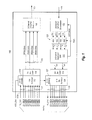
- Figure 1 illustrates a transponder system including a two-channel DP-QPSK modulator and a two-channel DP-QPSK demodulator according to some embodiments
- Figure 2 illustrates an example conceptualization for the two-channel DP-QPSK modulator of the transponder system of Figure 1 according to some embodiments
- Figure 3 illustrates a resulting four symbol IQ constellation graph according to some embodiments
- Figure 4 illustrates an example conceptualization for the two-channel DP-QPSK demodulator of the transponder system of Figure 1 according to some embodiments
- Figures 5A-5B illustrate aspects of a receive system including a DP-QPSK demodulator according to some embodiments
- Figure 6A illustrates a perspective view of an example DP-QPSK demodulator such as may be implemented in the transponder system of Figure 1 ;
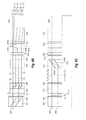
- Figure 6B illustrates a top view of the DP-QPSK demodulator of Figure 6A ;
- Figure 6C illustrates a side view of the DP-QPSK demodulator of Figure 6A ;
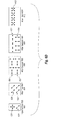
- Figure 6D illustrates various polarization states associated with various signals at various points during passage through the DP-QPSK demodulator of Figure 6A
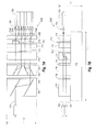
- Figure 7A illustrates a top view of another embodiment of a DP-QPSK demodulator such as may be implemented in the transponder system of Figure 1 ;
- Figure 7B illustrates a side view of the DP-QPSK demodulator of Figure 7A ;
- Figure 7C illustrates a top view of yet another embodiment of a DP-QPSK demodulator such as may be implemented in the transponder system of Figure 1 ;
- Figure 7D illustrates a side view of the DP-QPSK demodulator of Figure 7C .
- FIG. 1 illustrates a transponder system 100 (hereinafter "system 100") in which some embodiments disclosed herein may be implemented.
- system 100 is discussed below in an example implementation as a 100G DWDM OTU4 system, with the understanding that the system 100 is not confined to implementation as a 100G DWDM OTU4 system, but may be adapted to suit any particular network standard, data rate, or the like. While the system 100 will be described in some detail, the system 100 is not intended to limit the present disclosure and is merely provided as an example of a system in which some embodiments can be implemented. Moreover, in some embodiments, the elements of system 100 may be packaged as an optoelectronic module.
- the system 100 receives 11 lanes (labeled collectively 111) of 11 Gigabits per second data.
- One lane 111A is received into an SFI-S decoder 112, and the remaining 10 lanes are received into a 10:4 serializer 113.
- the SFI-S decoder 112 and the serializer 113 receive a reference clock signal REF_CLK in order to maintain proper timing.
- the data is reduced to four lanes (labeled collectively 115) of 28 Gigabit per second data after being properly encoded using pre-coder 114.
- a two-channel DP-QPSK modulator 116 applies DP-QPSK modulation to the four lanes of data to thereby modulate all four lanes of data onto a single optical fiber 117.
- the modulation is accomplished by using both an X polarization and an orthogonal Y polarization of the optical signal as orthogonal information transport mechanisms, and also by using the in-phase and quadrature-phase portions of each polarization.
- a receive optical signal (at a 112 Gigabit per second data rate) is received from the optical fiber 121 into a two-channel DP-QPSK demodulator 122.
- the received optical signal may be formulated by another network node in the same manner as the optical signal that was transmitted by DP-QPSK modulator 116.
- the two-channel DP-QPSK demodulator 122 extracts four components of the optical signal as follows: 1) an in-phase portion of the signal that had X polarization (labeled X-I), 2) a quadrature-phase portion of the signal that had X polarization (labeled X-Q), 3) an in-phase portion of the signal that had Y polarization (labeled Y-I), and 4) a quadrature-phase portion of the signal that had Y polarization (labeled Y-Q).
- Each of the X and Y polarizations has a bit rate of 56 Gigabits per second, and a symbol rate of 28 Gigasymbols per second, the symbols each representing two bits of information.
- the four demodulated data signals X-I, X-Q, Y-I and Y-Q are then quantized by a bank of four Analog-to-Digital Converters ("ADCs") 123. Each ADC quantizes the corresponding demodulated data signal into an n1 bit digital signal, which is then provided to a two-channel baseband Digital Signal Processor (“DSP”) 124.
- a local oscillator control signal "LO Control” is provided by the DSP 124 to the demodulator 122 thereby enabling a coherent receiver architecture.
- the DSP 124 identifies a corresponding point in an IQ symbol constellation chart for each of the X and Y polarizations, and outputs the corresponding 2 bit sequence for each.
- the bit sequences are decoded by the decoder 125, after which the 4:10 deserializer 126 and SFI-S encoder 127 deserializes the bits into 11 lanes (referenced collectively as 128) of SFI-S encoded data, each at approximately 11 Gigabits per second.
- FIG. 2 illustrates an example conceptualization 200 for the two-channel DP-QPSK modulator 116 of Figure 1 .
- There are two polarization branches in Figure 2 an X polarization branch represented by the upper circuitry, and a Y polarization branch represented by the lower circuitry.
- Portions of a local oscillator (“LO") signal provided by a distributed feedback (“DFB”) laser 201 or other LO source are fed into each polarization branch via the use of a power splitter 202.
- LO local oscillator
- DFB distributed feedback
- the continuous waveform from the DFB 201 is fed into a hybrid IQ circuit 211, which essentially causes a continuous in-phase waveform to be provided to an in-phase modulator 212A, and a 90 degree phase shifted version of the continuous waveform (i.e., a quadrature-phase waveform) to be provided to the quadrature-phase modulator 212B.
- a distinct 28 Gigabit per second signal is fed into each of the in-phase modulator 212A and the quadrature-phase modulator 212B causing appropriate phase shift keying of the optical signal.
- the in-phase and quadrature-phase keyed optical signals are then summed using optical summer 213.
- the Y branch includes hybrid IQ circuit 221, in-phase modulator 222A, quadrature-phase modulator 222B, and summer 223, which may essentially be the same as the respective components 211, 212A, 212B, and 213 of the X branch. However, the Y branch receives its own distinct pair of 28 Gigabits per second signals for appropriate phase shift keying.
- an X to Y rotator 224 is provided to represent the summed keyed optical signals output by summer 223 using Y polarization. The X polarized signal and the Y polarized signal are then summed using optical summer 203, after which the summed optical signal may then be transmitted onto an optical fiber.
- Figure 3 illustrates a four symbol constellation IQ graph 300 that results from each of the Y polarization signal and the X polarization signal.
- the magnitude of the in-phase component and the quadrature-phase component is calculated. Based on that information, the closest symbol point is selected from the IQ graph 300.
- the corresponding 2 bit symbol (herein m1 is equal to 2) is then output to the decoder 125. This is done for each of the X and Y polarization signals.
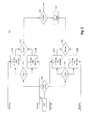
- Figure 4 illustrates an example conceptualization 400 for the two-channel demodulator 122 of Figure 1 .
- the optical signal is received into the X Y splitter 401, which provides the X polarized portion of the optical signal to the I/Q hybrid mixer 411 to start the X branch of demodulation.
- the X Y splitter 401 also provides the Y polarized portion of the optical signal to the Y to X rotator 402, which rotates the polarization of that optical signal to X polarization. That optical signal is provided to the I/Q hybrid mixer 421 to start the Y branch of demodulation.
- the X and Y polarization optical signals are mixed in I/Q Hybrids 411 and 421 respectively with a continuous waveform LO signal provided by a DFB laser 402 via the power splitter 403 with the timing of the continuous waveform controlled by the LO Control signal.
- the resulting mixed signals are then provided to corresponding optical detectors 412A, 412B, 422A and 422B.
- Each corresponding electrical signal may be adjusted to a normalized level by respective Variable Gain Amplifiers ("VGAs”) 413A, 413B 423A and 423B, after which they are subjected to clock recovery 414A, 414B, 424A and 424B.
- VGAs Variable Gain Amplifiers
- the clock recovery elements 414A, 414B, 424A and 424B should be viewed as functional transformations only, since the clock recovery may be provided for all channels using a single clock recovery circuit. This results in signals X-I, X-Q, Y-I and Y-Q described in Figure 1 .
- the VGA and Clock Recovery performance may be improved by using error signals derived in a corresponding two-channel Baseband DSP, such as the two-channel Baseband DSP 124 of Figure 1 .
- optical detectors 412A, 412B, 422A, 422B of Figure 4 may be implemented as four single-ended optical-to-electrical (hereinafter "opto-electrical") converters.
- suitable opto-electrical converters include, for instance, positive-intrinsic-negative (“PIN”) photodiodes, or the like.
- PIN positive-intrinsic-negative
- each of optical detectors 412A, 412B, 422A, 422B may include a pair of balanced opto-electrical converters.
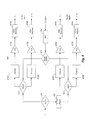
- FIG 5A illustrates a receive system 500 according to some embodiments.
- the receive system 500 may be implemented in a transponder system, such as the system 100 of Figure 1 .
- the receive system 500 may correspond to at least a portion of the receive side of system 100, including the two-channel DP-QPSK demodulator 122, ADCs 123 and two-channel Baseband DSP 124.
- the receive system 500 includes DP-QPSK demodulator 502, a plurality of optical detectors 504, a plurality of amplifiers 506, a plurality of ADCs 508, and DSP 510.
- the optical detectors 504 may include, for instance, four single-ended opto-electrical converters, or eight balanced opto-electrical converters arranged in pairs, or any other suitable configuration.
- the demodulator 502 is configured to receive a DP-QPSK optical signal 512 and an LO optical signal 514 generated by a local oscillator 516 such as a DFB laser.
- a local oscillator 516 such as a DFB laser.
- Each of DP-QPSK optical signal 512 and LO optical signal 514 is split into two components by one or more polarization beam splitters (“PBS”) 518.
- PBS polarization beam splitters
- the DP-QPSK optical signal 512 is split into a first component 512A having a first polarization state (e.g., X polarization) and a second component 512B having a second polarization state (e.g., Y polarization) that is orthogonal to the first polarization state.
- the first component 512A is provided to a first 90 degree hybrid mixer 522A.
- the second component 512B is provided to a second 90 degree hybrid mixer 522B.
- the LO optical signal 514 is also split into first and second components 514A, 514B that are respectively provided to the first and second 90 degree hybrid mixers 522A, 522B.
- the first 90 degree hybrid mixer 522A is configured to perform four 90 degree phase stepped interferences between the first component 512A of the DP-QPSK optical signal 512 and the first component 514A of the LO optical signal 514.
- the first 90 degree hybrid mixer 522A is configured to output four interference signals, including two in-phase signals S x + L x and S x - L x , and two quadrature-phase signals S x + jL x and S x - jL x .
- the "x" subscript denotes that these interference signals are associated with the X-polarized first component 512A of the DP-QPSK optical signal 512.
- the interference signals S x + L x , S x - L x , S x + jL x and S x - jL x output by the first 90 degree hybrid mixer 522A are converted to electrical signals by two pairs 504A, 504B of balanced opto-electrical converters included in the optical detectors 504.
- the first 90 degree hybrid mixer 522A may be configured to output two interference signals, including a single in-phase signal and a single quadrature-phase signal, and provide the two interference signals to two single-ended opto-electrical converters (not shown) included in the optical detectors 504.
- the second 90 degree hybrid mixer 522B is configured to perform four 90 degree phase stepped interferences between the second component 512B of the DP-QPSK optical signal 512 and the second component 514A of the LO optical signal 514.
- the second 90 degree hybrid mixer 522B is configured to output four interference signals, including two in-phase signals S y + L y and S y - L y , and two quadrature-phase signals S y + jL y and S y - jL y .
- the "y" subscript denotes that these interference signals are associated with the Y-polarized second component 512B of the DP-QPSK optical signal 512.
- the interference signals S y + L y , S y - L y , S y + jL y and S y - jL y output by the second 90 degree hybrid mixer 522B are converted to electrical signals by two pairs 504C, 504D of balanced opto-electrical converters included in the optical detectors 504.
- the second 90 degree hybrid mixer 522B may be configured to output two interference signals, including a single in-phase signal and a single quadrature-phase signal, and provide the two interference signals to two single-ended opto-electrical converters (not shown) included in the optical detectors 504.
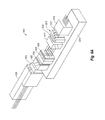
- Figure 6A-6C an example DP-QPSK demodulator 600 is illustrated according to some embodiments.
- Figure 6A is a perspective view
- Figure 6B is a top view
- Figure 6C is a side view of the DP-QPSK demodulator 600.
- the DP-QPSK demodulator 600 includes a first polarization beam splitter ("PBS") 602, a first half waveplate ("HWP") 604, a second PBS 606, a second HWP 608, a third PBS 610, and a third HWP 612.
- the DP-QPSK demodulator 600 further includes a quarter waveplate (“QWP) 614, an optical path compensator 616, and a beam displacer ("BD”) 618.
- QWP quarter waveplate
- BD beam displacer
- the foregoing components of DP-QPSK demodulator 600 may be formed on or otherwise coupled to a substrate 619.
- the substrate 619 may include fused silica or other suitable substrate material.
- the first HWP 604 is positioned to receive an output of the first PBS 602.
- the first HWP 604 may be coupled to the first PBS 602.
- the second PBS 606 is positioned to receive an output of the first HWP 604.
- the second HWP 608 is positioned to receive an output of the second PBS 606.
- the second HWP 608 may be coupled to the second PBS 606.
- the third PBS 610 is positioned to receive an output of the second HWP 608.
- the third HWP 612 is positioned to receive an output of the third PBS 610.
- the optical path compensator 616 is positioned between the third PBS 610 and the third HWP 612.
- the QWP 614 is positioned between the third PBS 610 and the optical path compensator 616.
- the QWP 614 is coupled to the optical path compensator 616.
- the BD 618 is positioned to receive an output of the third HWP 612.
- the third HWP 612 is coupled to the BD 618.
- a fiber array 620 contains a signal mode fiber and polarization-maintaining ("PM") fiber, which may be provided for signal and LO optical inputs. Alternately or additionally, a lens array 624 may be provided for beam collimating.
- PM polarization-maintaining
- a single DP-QPSK signal 626 enters the first PBS 602.
- the first PBS 602 divides the DP-QPSK signal 626 into signal components S x and S y having orthogonal X and Y polarization states.
- the DP-QPSK signal 626 includes first and second orthogonally polarized signal components S x and S y that share a common optical signal path.
- the first PBS 602 separates the signal components S x and S y onto separate signal paths.
- the orthogonal polarization states X and Y at the input of the first PBS 602 are illustrated at 628 in Figure 6D .
- the signal components S x and S y pass through the first HWP 604.
- a first portion of the first HWP 604 through which the signal component S x passes is oriented at about 22.5 degrees
- a second portion of the first HWP 604 through which the signal component S y passes is oriented at about -22.5 degrees.
- the term "oriented at” refers to the orientation of the optical axis angle of a waveplate crystal with respect to the horizontal line.
- the first HWP 604 rotates the polarization states 628 ( Figure 6D ) of the signal components S x and S y to the polarization states denoted at 629 in Figure 6D .
- the second PBS 606 divides signal component S x into two signal components S x1 and S x2 on separate signal paths and having orthogonal polarizations (e.g., horizontal and vertical polarizations, respectively). Additionally, the second PBS 606 divides signal component S y into two signal components S y1 and S y2 on separate signal paths and having orthogonal polarizations (e.g., horizontal and vertical polarizations, respectively).
- the respective polarization states of signal components S x1 , S x2 , S y1 and S y2 at the output of the second PBS 606 are denoted at 630 in Figure 6D .
- the signal components S x1 , S x2 , S y1 and S y2 next pass through the second HWP 608.
- the second HWP 608 rotates the polarization states 630 of the signal components S x1 , S x2 , S y1 and S y2 to the polarization states denoted at 631 in Figure 6D .
- a single LO signal 632 enters the first PBS 602.
- the LO signal 632 may have a linear polarization state such as the polarization state denoted at 634 in Figure 6D .
- the first PBS 602 divides the LO signal 632 into LO components L x and L y ( Figure 6C ) on separate signal paths and having orthogonal X and Y polarization states.
- the signal paths of the LO components L x and L y may generally be similar to the signal paths of signal components S x and S y shown in Figure 6B , although vertically displaced therebelow in the illustrated embodiment.
- the LO components L x and L y pass through the first HWP 604.
- LO component L x passes through the first portion of the first HWP 604, which is oriented at about 22.5 degrees
- LO component L y passes through the second portion of the first HWP 604, which is oriented at about -22.5 degrees.
- the first HWP 604 rotates the polarization states 628 ( Figure 6D ) of the LO components L x and L y to the polarization states denoted at 636 in Figure 6D .
- the second PBS 606 divides LO component L x into two components L x1 and L x2 ( Figure 6C ) on separate signal paths and having orthogonal polarizations (e.g., horizontal and vertical polarizations, respectively). Additionally, the second PBS 606 divides LO component L y into two components L y1 and L y2 ( Figure 6C ) on separate signal paths and having orthogonal polarizations (e.g., horizontal and vertical polarizations, respectively).
- the respective polarization states of components L x1 , L x2 , L y1 and L y2 at the output of the second PBS 606 are denoted at 637 in Figure 6D .
- the signal paths of components L x1 , L x2 , L y1 and L y2 may generally be similar to the signal paths of signal components S x1 , S x2 , S y1 and S y2 shown in Figure 6B , although vertically displaced therebelow in the illustrated embodiment.
- the components L x1 , L x2 , L y1 and L y2 next pass through the second HWP 608.
- portions of the second HWP 608 through which signal components S x1 , S y1 and components L x2 , L y2 pass are oriented at about 0 degrees
- portions of the second HWP 608 through which signal components S x2 , S y2 and components L x1 , L y1 pass are oriented at about 45 degrees.
- the second HWP 608 rotates the polarization states 637 of the components L x1 , L x2 , L y1 and L y2 to the polarization states denoted at 638 in Figure 6D .
- the polarization states 638 of components L x1 , L x2 , L y1 and L y2 are orthogonal to the polarization states 631 of signal components S x1 , S x2 , S y1 and S y2 .
- the third PBS 610 includes first and second interfaces 610A, 610B.
- the third PBS 610 may be configured such that the signal components S x1 , S x2 , S y1 and S y2 are transmitted through the first interface 610A.
- the third PB S 610 may be further configured to reflect components L x1 , L x2 , L y1 and L y2 at both the second and first interfaces 610B, 610A so as to redirect components L x1 , L x2 , L y1 and L y2 such that they occupy the same signal paths as signal components S x1 , S x2 , S y1 and S y2 .
- the components L x1 , L x2 , L y1 and L y2 are orthogonal to the polarization states 631 of signal components S x1 , S x2 , S y1 and S y2 , the components L x1 , L x2 , L y1 , and L y2 do not interfere with signal components S x1 , S x2 , S y1 and Sy 2 , despite sharing common signal paths.
- a first signal pair 640A including signal component S x2 and component L x2 passes through QWP 614.
- a second signal pair 640B including signal component S y1 and component L y1 also passes through QWP 614.
- the QWP 614 is oriented at about 0 degrees.
- a third signal pair 640C includes signal component S x1 and component L x1 and a fourth signal pair 640D includes signal component S y2 and component L y2 .
- the QWP 614 may be configured to produce a 90 degree phase difference between signal pairs 640A, 640B and signal pairs 640C, 640D.
- the first, second, third and fourth signals pairs 640A-640D pass through the compensator 616.
- the compensator 616 is configured to compensate for the different time delays experienced by the different signal components S x1 , S x2 , S y1 and S y2 due to different path lengths traveled through the DP-QPSK demodulator 600 such that they all have the same time delay after exiting the DP-QPSK demodulator 600.
- the compensator 616 may include crown glass or other suitable material.
- the compensator 616 includes a borosilicate glass composition.
- the compensator 616 may include a compensator commonly referred to as a bk7 compensator marketed by the Schott AG company.
- the signal pairs 640A-640D next pass through the third HWP 612.
- the third HWP 612 is oriented at about 22.5 degrees.
- the third HWP 612 rotates the polarization states of the signal pairs 640A-640D to the polarization states denoted at 642 in Figure 6D .
- the polarization state for each signal pair 640A-640D includes a first polarization state corresponding to component L x1 , L x2 , L y1 or L y2 , and a second polarization state corresponding to signal component S x1 , S x2 , S y1 or S y2 , respectively, the second polarization state being orthogonal to the first polarization state.
- the signal pairs 640A-640D enter the BD 618.
- the BD 618 divides the signal component S x1 into two components having orthogonal polarization states, e.g., vertical and horizontal polarization states, on separate signal paths.
- the two components of signal component S x1 may have substantially equal power in some embodiments.
- the BD 618 divides the component L x1 into two components having orthogonal polarization states, e.g., vertical and horizontal polarization states, on separate signal paths that are the same as the signal paths of the components of signal component S x1 .
- the two components of component L x1 may have substantially equal power in some embodiments.
- the components of signal component S x1 may interfere constructively and destructively with the respective components of component L x1 after being polarization-matched by the BD 618.
- constructive interference occurs between the components of each of signal component S x1 and component L x1 having the vertical polarization state to produce in-phase signal S x + L x ( Figure 6B ).
- destructive interference occurs between the components of each of signal component S x1 and component L x1 having the horizontal polarization state to produce in-phase signal S x - L x ( Figure 6B ).
- In-phase signals S x + L x and S x - L x may then be provided to a pair of balanced opto-electrical converters (not shown).
- the BD 618 divides each of signal components S x2 , S y1 and S y2 into two components having orthogonal polarization states on separate signal paths and divides each of components L x2 , L y1 and L y2 into two components having orthogonal polarization states on respective separate signal paths. Then, the components of signal component S x2 , S y1 and S y2 constructively and destructively interfere with the respective components of component L x2 , L y1 and L y2 .
- the DP-QPSK demodulator 600 of Figures 6A-6C is merely illustrative of a DP-QPSK according to some embodiments.
- Various adjustments and modifications can be made to the DP-QPSK demodulator 600 of Figures 6A-6C within the scope of the disclosed embodiments.
- Figures 7A-7B include a top view and a side view of an alternative embodiment of a DP-QPSK demodulator 700A that is similar in some respects to the DP-QPSK demodulator 600 of Figures 6A-6C .
- the DP-QPSK demodulator 700A includes a first PBS 702, a first HWP 704, a second PBS 706, a second HWP 708, a third PBS 710, and a third HWP 712.
- the DP-QPSK demodulator 700A further includes a QWP 714, an optical path compensator 716, and a BD 718.
- the first HWP 704 is positioned to receive an output of the first PBS 702.
- the first HWP 704 may be coupled to the first PBS 702.
- the second PBS 706 is positioned to receive an output of the first HWP 704.
- the second HWP 708 is positioned to receive an output of the second PBS 706.
- the second HWP 708 may be coupled to the second PBS 706.
- the third PBS 710 is positioned to receive an output of the second HWP 708.
- the third HWP 712 is positioned to receive an output of the third PBS 710.
- the third HWP 712 may be coupled to the optical path compensator 716.
- the optical path compensator 716 is positioned to receive an output of the third PBS 710.
- the QWP 714 is positioned between the third PBS 710 and the optical path compensator 716.
- the QWP 714 is coupled to the third HWP 712.
- the BD 718 is positioned to receive an output of the optical path compensator 716.
- the foregoing components of DP-QPSK demodulator 700A may be formed on or otherwise coupled to a substrate 719 ( Figure 7B ).
- the substrate 719 may include fused silica or other suitable substrate material.
- the DP-QPSK demodulator 700A is generally analogous to the operation of the DP-QPSK demodulator 600 of Figures 6A-6C and will not be described in detail.
- the DP-QPSK demodulator is configured to perform phase stepped interferences between both an X-polarization component and a Y-polarization component of an incoming DP-QPSK signal 720 and an LO signal 722 to produce four in-phase signals 724 ( Figure 7A ), including a first pair 724A (e.g., S x + L x and S x - L x ) from the X-polarization component, and a second pair 724B (e.g., S y + L y and S y - L y ) from the Y-polarization component, and to produce four quadrature-phase signals 726 ( Figure 7A ), including a first pair 726A (e.g., S x + jL x and S x -
- the DP-QPSK demodulator 700A may further include a plurality of optical fibers 728 positioned to receive the paired optical signals 724A, 726A, 724B, 726B that are output from the BD 718.
- the optical fibers 728 may include an 8 x 125 micrometer (“ ⁇ m”) ribbon fiber in some embodiments.
- the DP-QPSK demodulator 700A may further include a lens array 730 positioned between the BD 718 and the optical fibers 728.
- the DP-QPSK demodulator 700A has a length I ( Figure 7B ) of about 14 millimeters ("mm"), a height h ( Figure 7B ) of about 2 mm, and a width w ( Figure 7A ) of about 2.4 mm.
- Figures 7C-7D illustrate another alternative embodiment of a DP-QPSK demodulator 700B according to some embodiments.
- Figure 7C is a top view and Figure 7D is a side view of the DP-QPSK demodulator 700B.
- the DP-QPSK demodulator 700B is similar in some respects to the DP-QPSK demodulator 700A of Figures 7A-7B and like reference numbers denote like elements. Additional details regarding the arrangement and operation of the DP-QPSK demodulator 700B of Figures 7C-7D are provided above with respect to the DP-QPSK demodulator 700A of Figures 7A-7B .
- the DP-QPSK demodulator 700B may further include a plurality of balanced opto-electrical converters 732 positioned to receive the paired optical signals 724A, 726A, 724B, 726B that are output from the BD 718.
- the lens array 730 may be positioned between the BD 718 and the balanced opto-electrical converters 732.
Landscapes
- Physics & Mathematics (AREA)
- Electromagnetism (AREA)
- Engineering & Computer Science (AREA)
- Computer Networks & Wireless Communication (AREA)
- Signal Processing (AREA)
- Optical Communication System (AREA)
Abstract
Description
- The present invention generally relates to optical communication systems. More particularly, some example embodiments relate to a dual-polarization ("DP")-quadrature phase shift keyed ("QPSK") demodulator that may be used in some optical communication systems.
- Communication technology has transformed our world. As the amount of information communicated over networks has increased, high speed transmission has become ever more critical. High speed communications often rely on the presence of high bandwidth capacity links between network nodes. For optical links, an optoelectronic m odule such as a transceiver or transponder module at one network node converts electrical data into optical data for transmission on the optical channel. At the other network node, another transceiver module receives the optical signal, and converts the signal into an electrical signal. Transceivers are equipped with transmit and receive channels, such that bi-directional communication is possible.
- Presently, standards are being developed for optical links at a staggering speed of 100 Gigabits per second (sometimes abbreviated as "100G"). In fact, the Institute for Electrical and Electronics Engineers, Inc. (often referred to as "IEEE" for short), a leading professional association in the art of networking technologies, has recently voted that the next generation of Ethernet technology will be 100 Gigabit Ethernet as well as some support for 40 Gigabit Ethernet, and has established several task forces to develop appropriate standards that are yet under development.
- Currently, 100G Single Mode Fiber ("SMF") and Multi Mode Fiber ("MMF") standards for Ethernet optical link applications are under development. In general, however, on the transmit side, it is presently contemplated that such high speed transmitters will include a Media Access Control ("MAC") component that provides data electrically to an optical transmitter. However, since 100 Gigabits per second is simply too fast for present Complementary Metal Oxide Semiconductor ("CMOS") electrical I/O technology, the 100 Gigabits of electrical data will be provided in several independent electrical lanes.
- For instance, perhaps 10 lanes of 10 Gigabits per second of data will be provided from the MAC component to the transmitter. If there were additional overhead used for encoding or error correction, perhaps the data rate for each lane may be increased and/or the number of lanes may be increased. For instance, 66B/64B encoding has been contemplated as being used to encode each lane of 10 Gigabits per second. This would result in each of the 10 lanes of electrical traffic being at an actual data rate of 10.3125 Gigabits per second.
- In the transmitter, the 10 lanes of electrical traffic are serialized down to perhaps 4 lanes of optical data, each at a data rate of 25.78125 Gigabits per second, which includes the overhead for 66B/64B encoding. These 4 lanes of optical data may then be multiplexed onto a signal fiber using Wavelength Division Multiplexing ("WDM").
- Ethernet data may be transported over longer distances by Dense Wavelength Division Multiplexing ("DWDM") systems. Currently, standards are under development for defining the use of DWDM technology for transporting 100G Ethernet data. The standard is referred to as OTU4 and encapsulates the Ethernet data in a payload which is then Forward Error Correction ("FEC") encoded. The resulting fiber data rate is approximately 112 Gigabits per second.
- The system (hereinafter called the "100G DWDM OTU4 system") is contemplated as including two primary components, a Forward Error Correction capable MAC layer (called hereinafter an "OTU4/FEC processor") and a 100G DWDM capable transponder. In each of the transmit and receive channels, there are 10 lanes of 11 Gigabits per second data that are communicated using the OIF SFI-S interface specification. There is also an eleventh de-skew lane to align all 10 data lanes for serial data transmission.
- One of the modulation technologies considered in this 100G DWDM OTU4 system is Dual-Polarization Quadrature Phase-Shift Keying (called "DP-QPSK" for short). The 112 Gigabit per second data stream is contemplated to be divided into four 28Gb/s data streams, and modulates both I and Q phases of two orthogonally polarized optical carriers having the same wavelength that are transmitted as a single DP-QPSK signal.
- On the receive side, an incoming DP-QPSK signal is separated into two orthogonally polarized optical carriers that are processed by a DP-QPSK demodulator to extract the modulation of the I and Q phases of each of the orthogonally polarized optical signals.
- The subject matter claimed herein is not limited to embodiments that solve any disadvantages or that operate only in environments such as those described above. Rather, this background is only provided to illustrate one exemplary technology area where some embodiments described herein may be practiced.
- Some example embodiments generally relate to a DP-QPSK demodulator.
- In an embodiment, a DP-QPSK demodulator includes first, second and third polarization beam splitters ("PBSs") and first, second and third half waveplates ("HWPs"). The first HWP is positioned to receive an output of the first PBS. The second PBS is positioned to receive an output of the first HWP. The second HWP is positioned to receive an output of the second PBS. The third PBS is positioned to receive an output of the second HWP. The third HWP is positioned to receive an output of the third PBS.
- In an embodiment, an optoelectronic module includes a DP-QPSK demodulator, a plurality of optical detectors, and a digital signal processor ("DSP"). The DP-QPSK demodulator includes first, second and third PBSs and first, second and third HWPs. The first HWP is positioned to receive an output of the first PBS. The second PBS is positioned to receive an output of the first HWP. The second HWP is positioned to receive an output of the second PBS. The third PBS is positioned to receive an output of the second HWP. The third HWP is positioned to receive an output of the third PBS. The optical detectors are positioned to receive a plurality of optical signals output by the DP-QPSK demodulator and are configured to convert the plurality of optical signals to a plurality of electrical signals. The DSP is electrically coupled to respective outputs of the plurality of optical detectors.
- This Summary is provided to introduce a selection of concepts in a simplified form that are further described below in the Detailed Description. This Summary is not intended to identify key features or essential characteristics of the claimed subject matter, nor is it intended to be used as an aid in determining the scope of the claimed subject matter.
- Additional features and advantages of the invention will be set forth in the description which follows, and in part will be obvious from the description, or may be learned by the practice of the invention. The features and advantages of the invention may be realized and obtained by means of the instruments and combinations particularly pointed out in the appended claims. These and other features of the present invention will become more fully apparent from the following description and appended claims, or may be learned by the practice of the invention as set forth hereinafter.
- To further clarify the above and other advantages and features of the present invention, a more particular description of the invention will be rendered by reference to specific embodiments thereof which are illustrated in the appended drawings. It is appreciated that these drawings depict only typical embodiments of the invention and are therefore not to be considered limiting of its scope. The invention will be described and explained with additional specificity and detail through the use of the accompanying drawings in which:
-
Figure 1 illustrates a transponder system including a two-channel DP-QPSK modulator and a two-channel DP-QPSK demodulator according to some embodiments; -
Figure 2 illustrates an example conceptualization for the two-channel DP-QPSK modulator of the transponder system ofFigure 1 according to some embodiments; -
Figure 3 illustrates a resulting four symbol IQ constellation graph according to some embodiments; -
Figure 4 illustrates an example conceptualization for the two-channel DP-QPSK demodulator of the transponder system ofFigure 1 according to some embodiments; -
Figures 5A-5B illustrate aspects of a receive system including a DP-QPSK demodulator according to some embodiments; -
Figure 6A illustrates a perspective view of an example DP-QPSK demodulator such as may be implemented in the transponder system ofFigure 1 ; -
Figure 6B illustrates a top view of the DP-QPSK demodulator ofFigure 6A ; -
Figure 6C illustrates a side view of the DP-QPSK demodulator ofFigure 6A ; -
Figure 6D illustrates various polarization states associated with various signals at various points during passage through the DP-QPSK demodulator ofFigure 6A -
Figure 7A illustrates a top view of another embodiment of a DP-QPSK demodulator such as may be implemented in the transponder system ofFigure 1 ; -
Figure 7B illustrates a side view of the DP-QPSK demodulator ofFigure 7A ; -
Figure 7C illustrates a top view of yet another embodiment of a DP-QPSK demodulator such as may be implemented in the transponder system ofFigure 1 ; and -
Figure 7D illustrates a side view of the DP-QPSK demodulator ofFigure 7C . - Reference will now be made to the drawings to describe various aspects of example embodiments of the invention. It is to be understood that the drawings are diagrammatic and schematic representations of such example embodiments, and are not limiting of the present invention, nor are they necessarily drawn to scale.
-
Figure 1 illustrates a transponder system 100 (hereinafter "system 100") in which some embodiments disclosed herein may be implemented. Thesystem 100 is discussed below in an example implementation as a 100G DWDM OTU4 system, with the understanding that thesystem 100 is not confined to implementation as a 100G DWDM OTU4 system, but may be adapted to suit any particular network standard, data rate, or the like. While thesystem 100 will be described in some detail, thesystem 100 is not intended to limit the present disclosure and is merely provided as an example of a system in which some embodiments can be implemented. Moreover, in some embodiments, the elements ofsystem 100 may be packaged as an optoelectronic module. - On the transmit side, the
system 100 receives 11 lanes (labeled collectively 111) of 11 Gigabits per second data. Onelane 111A is received into an SFI-S decoder 112, and the remaining 10 lanes are received into a 10:4serializer 113. The SFI-S decoder 112 and theserializer 113 receive a reference clock signal REF_CLK in order to maintain proper timing. The data is reduced to four lanes (labeled collectively 115) of 28 Gigabit per second data after being properly encoded usingpre-coder 114. A two-channel DP-QPSK modulator 116 applies DP-QPSK modulation to the four lanes of data to thereby modulate all four lanes of data onto a singleoptical fiber 117. The modulation is accomplished by using both an X polarization and an orthogonal Y polarization of the optical signal as orthogonal information transport mechanisms, and also by using the in-phase and quadrature-phase portions of each polarization. - On the receive side, a receive optical signal (at a 112 Gigabit per second data rate) is received from the
optical fiber 121 into a two-channel DP-QPSK demodulator 122. The received optical signal may be formulated by another network node in the same manner as the optical signal that was transmitted by DP-QPSK modulator 116. The two-channel DP-QPSK demodulator 122 extracts four components of the optical signal as follows: 1) an in-phase portion of the signal that had X polarization (labeled X-I), 2) a quadrature-phase portion of the signal that had X polarization (labeled X-Q), 3) an in-phase portion of the signal that had Y polarization (labeled Y-I), and 4) a quadrature-phase portion of the signal that had Y polarization (labeled Y-Q). Each of the X and Y polarizations has a bit rate of 56 Gigabits per second, and a symbol rate of 28 Gigasymbols per second, the symbols each representing two bits of information. - The four demodulated data signals X-I, X-Q, Y-I and Y-Q are then quantized by a bank of four Analog-to-Digital Converters ("ADCs") 123. Each ADC quantizes the corresponding demodulated data signal into an n1 bit digital signal, which is then provided to a two-channel baseband Digital Signal Processor ("DSP") 124. A local oscillator control signal "LO Control" is provided by the
DSP 124 to thedemodulator 122 thereby enabling a coherent receiver architecture. TheDSP 124 identifies a corresponding point in an IQ symbol constellation chart for each of the X and Y polarizations, and outputs the corresponding 2 bit sequence for each. The bit sequences are decoded by thedecoder 125, after which the 4:10 deserializer 126 and SFI-S encoder 127 deserializes the bits into 11 lanes (referenced collectively as 128) of SFI-S encoded data, each at approximately 11 Gigabits per second. -
Figure 2 illustrates anexample conceptualization 200 for the two-channel DP-QPSK modulator 116 ofFigure 1 . There are two polarization branches inFigure 2 , an X polarization branch represented by the upper circuitry, and a Y polarization branch represented by the lower circuitry. Portions of a local oscillator ("LO") signal provided by a distributed feedback ("DFB")laser 201 or other LO source are fed into each polarization branch via the use of apower splitter 202. - As for the X branch, the continuous waveform from the
DFB 201 is fed into ahybrid IQ circuit 211, which essentially causes a continuous in-phase waveform to be provided to an in-phase modulator 212A, and a 90 degree phase shifted version of the continuous waveform (i.e., a quadrature-phase waveform) to be provided to the quadrature-phase modulator 212B. A distinct 28 Gigabit per second signal is fed into each of the in-phase modulator 212A and the quadrature-phase modulator 212B causing appropriate phase shift keying of the optical signal. The in-phase and quadrature-phase keyed optical signals are then summed usingoptical summer 213. - The Y branch includes
hybrid IQ circuit 221, in-phase modulator 222A, quadrature-phase modulator 222B, andsummer 223, which may essentially be the same as therespective components Y rotator 224 is provided to represent the summed keyed optical signals output bysummer 223 using Y polarization. The X polarized signal and the Y polarized signal are then summed usingoptical summer 203, after which the summed optical signal may then be transmitted onto an optical fiber. -
Figure 3 illustrates a four symbolconstellation IQ graph 300 that results from each of the Y polarization signal and the X polarization signal. There are four symbol points 301-304 shown in theIQ graph 300. When a particular signal is received for a certain polarization, the magnitude of the in-phase component and the quadrature-phase component is calculated. Based on that information, the closest symbol point is selected from theIQ graph 300. The corresponding 2 bit symbol (herein m1 is equal to 2) is then output to thedecoder 125. This is done for each of the X and Y polarization signals. -
Figure 4 illustrates anexample conceptualization 400 for the two-channel demodulator 122 ofFigure 1 . The optical signal is received into theX Y splitter 401, which provides the X polarized portion of the optical signal to the I/Q hybrid mixer 411 to start the X branch of demodulation. TheX Y splitter 401 also provides the Y polarized portion of the optical signal to the Y toX rotator 402, which rotates the polarization of that optical signal to X polarization. That optical signal is provided to the I/Q hybrid mixer 421 to start the Y branch of demodulation. - The X and Y polarization optical signals are mixed in I/
Q Hybrids DFB laser 402 via thepower splitter 403 with the timing of the continuous waveform controlled by the LO Control signal. The resulting mixed signals are then provided to correspondingoptical detectors 413B clock recovery clock recovery elements Figure 1 . The VGA and Clock Recovery performance may be improved by using error signals derived in a corresponding two-channel Baseband DSP, such as the two-channel Baseband DSP 124 ofFigure 1 . - The
optical detectors Figure 4 may be implemented as four single-ended optical-to-electrical (hereinafter "opto-electrical") converters. Examples of suitable opto-electrical converters include, for instance, positive-intrinsic-negative ("PIN") photodiodes, or the like. Alternatively, each ofoptical detectors -
Figure 5A illustrates a receive system 500 according to some embodiments. The receive system 500 may be implemented in a transponder system, such as thesystem 100 ofFigure 1 . In particular, the receive system 500 may correspond to at least a portion of the receive side ofsystem 100, including the two-channel DP-QPSK demodulator 122,ADCs 123 and two-channel Baseband DSP 124. - As shown, the receive system 500 includes DP-
QPSK demodulator 502, a plurality ofoptical detectors 504, a plurality ofamplifiers 506, a plurality ofADCs 508, and DSP 510. Theoptical detectors 504 may include, for instance, four single-ended opto-electrical converters, or eight balanced opto-electrical converters arranged in pairs, or any other suitable configuration. - Additional details regarding example embodiments of the
demodulator 502,optical detectors 504 andamplifiers 506 of the receive system 500 are provided inFigure 5B . As illustrated inFigure 5B , thedemodulator 502 is configured to receive a DP-QPSKoptical signal 512 and an LOoptical signal 514 generated by alocal oscillator 516 such as a DFB laser. Each of DP-QPSKoptical signal 512 and LOoptical signal 514 is split into two components by one or more polarization beam splitters ("PBS") 518. - In more detail, the DP-QPSK
optical signal 512 is split into afirst component 512A having a first polarization state (e.g., X polarization) and asecond component 512B having a second polarization state (e.g., Y polarization) that is orthogonal to the first polarization state. Thefirst component 512A is provided to a first 90 degreehybrid mixer 522A. Thesecond component 512B is provided to a second 90 degreehybrid mixer 522B. - The LO
optical signal 514 is also split into first andsecond components degree hybrid mixers - In general, the first 90 degree
hybrid mixer 522A is configured to perform four 90 degree phase stepped interferences between thefirst component 512A of the DP-QPSKoptical signal 512 and thefirst component 514A of the LOoptical signal 514. In the illustrated embodiment, the first 90 degreehybrid mixer 522A is configured to output four interference signals, including two in-phase signals Sx + Lx and Sx - Lx, and two quadrature-phase signals Sx + jLx and Sx - jLx. The "x" subscript denotes that these interference signals are associated with the X-polarizedfirst component 512A of the DP-QPSKoptical signal 512. - The interference signals Sx + Lx, Sx - Lx, Sx + jLx and Sx - jLx output by the first 90 degree
hybrid mixer 522A are converted to electrical signals by twopairs optical detectors 504. Alternatively, the first 90 degreehybrid mixer 522A may be configured to output two interference signals, including a single in-phase signal and a single quadrature-phase signal, and provide the two interference signals to two single-ended opto-electrical converters (not shown) included in theoptical detectors 504. - Analogously, the second 90 degree
hybrid mixer 522B is configured to perform four 90 degree phase stepped interferences between thesecond component 512B of the DP-QPSKoptical signal 512 and thesecond component 514A of the LOoptical signal 514. In the illustrated embodiment, the second 90 degreehybrid mixer 522B is configured to output four interference signals, including two in-phase signals Sy + Ly and Sy - Ly, and two quadrature-phase signals Sy + jLy and Sy - jLy. The "y" subscript denotes that these interference signals are associated with the Y-polarizedsecond component 512B of the DP-QPSKoptical signal 512. - The interference signals Sy + Ly, Sy - Ly, Sy + jLy and Sy - jLy output by the second 90 degree
hybrid mixer 522B are converted to electrical signals by twopairs optical detectors 504. Alternatively, the second 90 degreehybrid mixer 522B may be configured to output two interference signals, including a single in-phase signal and a single quadrature-phase signal, and provide the two interference signals to two single-ended opto-electrical converters (not shown) included in theoptical detectors 504. - Turning to
Figures 6A-6C , an example DP-QPSK demodulator 600 is illustrated according to some embodiments.Figure 6A is a perspective view,Figure 6B is a top view andFigure 6C is a side view of the DP-QPSK demodulator 600. As shown inFigures 6A-6C , the DP-QPSK demodulator 600 includes a first polarization beam splitter ("PBS") 602, a first half waveplate ("HWP") 604, asecond PBS 606, asecond HWP 608, athird PBS 610, and athird HWP 612. Alternately or additionally, the DP-QPSK demodulator 600 further includes a quarter waveplate ("QWP) 614, an optical path compensator 616, and a beam displacer ("BD") 618. - Optionally, the foregoing components of DP-
QPSK demodulator 600 may be formed on or otherwise coupled to asubstrate 619. Thesubstrate 619 may include fused silica or other suitable substrate material. - In
Figures 6A-6C , thefirst HWP 604 is positioned to receive an output of thefirst PBS 602. Optionally, thefirst HWP 604 may be coupled to thefirst PBS 602. Thesecond PBS 606 is positioned to receive an output of thefirst HWP 604. Thesecond HWP 608 is positioned to receive an output of thesecond PBS 606. Optionally, thesecond HWP 608 may be coupled to thesecond PBS 606. Thethird PBS 610 is positioned to receive an output of thesecond HWP 608. Thethird HWP 612 is positioned to receive an output of thethird PBS 610. The optical path compensator 616 is positioned between thethird PBS 610 and thethird HWP 612. TheQWP 614 is positioned between thethird PBS 610 and theoptical path compensator 616. Optionally, theQWP 614 is coupled to theoptical path compensator 616. TheBD 618 is positioned to receive an output of thethird HWP 612. Optionally, thethird HWP 612 is coupled to theBD 618. - As shown in
Figure 6A , afiber array 620 contains a signal mode fiber and polarization-maintaining ("PM") fiber, which may be provided for signal and LO optical inputs. Alternately or additionally, alens array 624 may be provided for beam collimating. - As best seen in
Figures 6B-6C , a single DP-QPSK signal 626 enters thefirst PBS 602. Thefirst PBS 602 divides the DP-QPSK signal 626 into signal components Sx and Sy having orthogonal X and Y polarization states. In other words, at the input of thefirst PBS 602, the DP-QPSK signal 626 includes first and second orthogonally polarized signal components Sx and Sy that share a common optical signal path. Thefirst PBS 602 separates the signal components Sx and Sy onto separate signal paths. The orthogonal polarization states X and Y at the input of thefirst PBS 602 are illustrated at 628 inFigure 6D . - Next, the signal components Sx and Sy pass through the
first HWP 604. In at least some example embodiments, a first portion of thefirst HWP 604 through which the signal component Sx passes is oriented at about 22.5 degrees, and a second portion of thefirst HWP 604 through which the signal component Sy passes is oriented at about -22.5 degrees. As used herein, the term "oriented at" refers to the orientation of the optical axis angle of a waveplate crystal with respect to the horizontal line. Thefirst HWP 604 rotates the polarization states 628 (Figure 6D ) of the signal components Sx and Sy to the polarization states denoted at 629 inFigure 6D . - Next, as best seen in
Figure 6B , thesecond PBS 606 divides signal component Sx into two signal components Sx1 and Sx2 on separate signal paths and having orthogonal polarizations (e.g., horizontal and vertical polarizations, respectively). Additionally, thesecond PBS 606 divides signal component Sy into two signal components Sy1 and Sy2 on separate signal paths and having orthogonal polarizations (e.g., horizontal and vertical polarizations, respectively). The respective polarization states of signal components Sx1, Sx2, Sy1 and Sy2 at the output of thesecond PBS 606 are denoted at 630 inFigure 6D . - The signal components Sx1, Sx2, Sy1 and Sy2 next pass through the
second HWP 608. Thesecond HWP 608 rotates the polarization states 630 of the signal components Sx1, Sx2, Sy1 and Sy2 to the polarization states denoted at 631 inFigure 6D . - Before proceeding at the
third PBS 610, we will briefly return to thefirst PBS 602. As best seen inFigure 6C , asingle LO signal 632 enters thefirst PBS 602. At the input of thefirst PBS 602, theLO signal 632 may have a linear polarization state such as the polarization state denoted at 634 inFigure 6D . Thefirst PBS 602 divides the LO signal 632 into LO components Lx and Ly (Figure 6C ) on separate signal paths and having orthogonal X and Y polarization states. The signal paths of the LO components Lx and Ly may generally be similar to the signal paths of signal components Sx and Sy shown inFigure 6B , although vertically displaced therebelow in the illustrated embodiment. - Next, the LO components Lx and Ly pass through the
first HWP 604. In at least some example embodiments, LO component Lx passes through the first portion of thefirst HWP 604, which is oriented at about 22.5 degrees, and LO component Ly passes through the second portion of thefirst HWP 604, which is oriented at about -22.5 degrees. Thefirst HWP 604 rotates the polarization states 628 (Figure 6D ) of the LO components Lx and Ly to the polarization states denoted at 636 inFigure 6D . - Next, the
second PBS 606 divides LO component Lx into two components Lx1 and Lx2 (Figure 6C ) on separate signal paths and having orthogonal polarizations (e.g., horizontal and vertical polarizations, respectively). Additionally, thesecond PBS 606 divides LO component Ly into two components Ly1 and Ly2 (Figure 6C ) on separate signal paths and having orthogonal polarizations (e.g., horizontal and vertical polarizations, respectively). The respective polarization states of components Lx1, Lx2, Ly1 and Ly2 at the output of thesecond PBS 606 are denoted at 637 inFigure 6D . Additionally, the signal paths of components Lx1, Lx2, Ly1 and Ly2 may generally be similar to the signal paths of signal components Sx1, Sx2, Sy1 and Sy2 shown inFigure 6B , although vertically displaced therebelow in the illustrated embodiment. - The components Lx1, Lx2, Ly1 and Ly2 next pass through the
second HWP 608. In at least some example embodiments, portions of thesecond HWP 608 through which signal components Sx1, Sy1 and components Lx2, Ly2 pass are oriented at about 0 degrees, and portions of thesecond HWP 608 through which signal components Sx2, Sy2 and components Lx1, Ly1 pass are oriented at about 45 degrees. Thesecond HWP 608 rotates the polarization states 637 of the components Lx1, Lx2, Ly1 and Ly2 to the polarization states denoted at 638 inFigure 6D . As seen inFigure 6D , the polarization states 638 of components Lx1, Lx2, Ly1 and Ly2 are orthogonal to the polarization states 631 of signal components Sx1, Sx2, Sy1 and Sy2. - As best seen with reference to
Figure 6C , thethird PBS 610 includes first andsecond interfaces third PBS 610 may be configured such that the signal components Sx1, Sx2, Sy1 and Sy2 are transmitted through thefirst interface 610A. Thethird PB S 610 may be further configured to reflect components Lx1, Lx2, Ly1 and Ly2 at both the second andfirst interfaces - A
first signal pair 640A including signal component Sx2 and component Lx2 passes throughQWP 614. A second signal pair 640B including signal component Sy1 and component Ly1 also passes throughQWP 614. In at least some example embodiments, theQWP 614 is oriented at about 0 degrees. Athird signal pair 640C includes signal component Sx1 and component Lx1 and afourth signal pair 640D includes signal component Sy2 and component Ly2. The QWP 614 may be configured to produce a 90 degree phase difference between signal pairs 640A, 640B and signal pairs 640C, 640D. - The first, second, third and fourth signals pairs 640A-640D pass through the
compensator 616. Thecompensator 616 is configured to compensate for the different time delays experienced by the different signal components Sx1, Sx2, Sy1 and Sy2 due to different path lengths traveled through the DP-QPSK demodulator 600 such that they all have the same time delay after exiting the DP-QPSK demodulator 600. Thecompensator 616 may include crown glass or other suitable material. In some embodiments, thecompensator 616 includes a borosilicate glass composition. Alternately or additionally, thecompensator 616 may include a compensator commonly referred to as a bk7 compensator marketed by the Schott AG company. - The signal pairs 640A-640D next pass through the
third HWP 612. In at least some example embodiments, thethird HWP 612 is oriented at about 22.5 degrees. Thethird HWP 612 rotates the polarization states of the signal pairs 640A-640D to the polarization states denoted at 642 inFigure 6D . In particular, the polarization state for eachsignal pair 640A-640D includes a first polarization state corresponding to component Lx1, Lx2, Ly1 or Ly2, and a second polarization state corresponding to signal component Sx1, Sx2, Sy1 or Sy2, respectively, the second polarization state being orthogonal to the first polarization state. - Next, the signal pairs 640A-640D enter the
BD 618. TheBD 618 divides the signal component Sx1 into two components having orthogonal polarization states, e.g., vertical and horizontal polarization states, on separate signal paths. The two components of signal component Sx1 may have substantially equal power in some embodiments. Similarly, theBD 618 divides the component Lx1 into two components having orthogonal polarization states, e.g., vertical and horizontal polarization states, on separate signal paths that are the same as the signal paths of the components of signal component Sx1. The two components of component Lx1 may have substantially equal power in some embodiments. - The components of signal component Sx1 may interfere constructively and destructively with the respective components of component Lx1 after being polarization-matched by the
BD 618. In particular, constructive interference occurs between the components of each of signal component Sx1 and component Lx1 having the vertical polarization state to produce in-phase signal Sx + Lx (Figure 6B ). Additionally, destructive interference occurs between the components of each of signal component Sx1 and component Lx1 having the horizontal polarization state to produce in-phase signal Sx - Lx (Figure 6B ). In-phase signals Sx + Lx and Sx - Lx may then be provided to a pair of balanced opto-electrical converters (not shown). - In an analogous manner, the
BD 618 divides each of signal components Sx2, Sy1 and Sy2 into two components having orthogonal polarization states on separate signal paths and divides each of components Lx2, Ly1 and Ly2 into two components having orthogonal polarization states on respective separate signal paths. Then, the components of signal component Sx2, Sy1 and Sy2 constructively and destructively interfere with the respective components of component Lx2, Ly1 and Ly2. - In particular, constructive interference occurs between the components of each of signal component Sx2 and component Lx2 having the vertical polarization state to produce quadrature-phase signal Sx + jLx (
Figure 6B ). Additionally, destructive interference occurs between the components of each of signal component Sx2 and component Lx2 having the horizontal polarization state to produce quadrature-phase signal Sx - jLx (Figure 6B ). Quadrature-phase signals Sx + jLx and Sx - jLx may then be provided to a pair of balanced opto-electrical converters (not shown). - Analogously, constructive interference occurs between the components of each of signal component Sy1 and component Ly1 having the vertical polarization state to produce in-phase signal Sy + Ly (
Figure 6B ). Additionally, destructive interference occurs between the components of each of signal component Sy1 and component Ly1 having the horizontal polarization state to produce in-phase signal Sy - Ly (Figure 6B ). In-phase signals Sy + Ly and Sy - Ly may then be provided to a pair of balanced opto-electrical converters (not shown). - Analogously, constructive interference occurs between the components of each of signal component Sy2 and component Ly2 having the vertical polarization state to produce quadrature-phase signal Sy + jLy (
Figure 6B ). Additionally, destructive interference occurs between the components of each of signal component Sy2 and component Ly2 having the horizontal polarization state to produce quadrature-phase signal Sy - jLy (Figure 6B ). Quadrature-phase signals Sy + jLy and Sy - jLy may then be provided to a pair of balanced opto-electrical converters (not shown). - The DP-
QPSK demodulator 600 ofFigures 6A-6C is merely illustrative of a DP-QPSK according to some embodiments. Various adjustments and modifications can be made to the DP-QPSK demodulator 600 ofFigures 6A-6C within the scope of the disclosed embodiments. For instance,Figures 7A-7B include a top view and a side view of an alternative embodiment of a DP-QPSK demodulator 700A that is similar in some respects to the DP-QPSK demodulator 600 ofFigures 6A-6C . For instance, the DP-QPSK demodulator 700A includes afirst PBS 702, afirst HWP 704, asecond PBS 706, asecond HWP 708, athird PBS 710, and athird HWP 712. Alternately or additionally, the DP-QPSK demodulator 700A further includes aQWP 714, an optical path compensator 716, and aBD 718. - In
Figures 7A-7B , thefirst HWP 704 is positioned to receive an output of thefirst PBS 702. Optionally, thefirst HWP 704 may be coupled to thefirst PBS 702. Thesecond PBS 706 is positioned to receive an output of thefirst HWP 704. Thesecond HWP 708 is positioned to receive an output of thesecond PBS 706. Optionally, thesecond HWP 708 may be coupled to thesecond PBS 706. Thethird PBS 710 is positioned to receive an output of thesecond HWP 708. Thethird HWP 712 is positioned to receive an output of thethird PBS 710. Optionally, thethird HWP 712 may be coupled to theoptical path compensator 716. The optical path compensator 716 is positioned to receive an output of thethird PBS 710. TheQWP 714 is positioned between thethird PBS 710 and theoptical path compensator 716. Optionally, theQWP 714 is coupled to thethird HWP 712. TheBD 718 is positioned to receive an output of theoptical path compensator 716. - Optionally, the foregoing components of DP-
QPSK demodulator 700A may be formed on or otherwise coupled to a substrate 719 (Figure 7B ). Thesubstrate 719 may include fused silica or other suitable substrate material. - Operation of the DP-
QPSK demodulator 700A is generally analogous to the operation of the DP-QPSK demodulator 600 ofFigures 6A-6C and will not be described in detail. Generally, however, the DP-QPSK demodulator is configured to perform phase stepped interferences between both an X-polarization component and a Y-polarization component of an incoming DP-QPSK signal 720 and anLO signal 722 to produce four in-phase signals 724 (Figure 7A ), including afirst pair 724A (e.g., Sx + Lx and Sx - Lx) from the X-polarization component, and asecond pair 724B (e.g., Sy + Ly and Sy - Ly) from the Y-polarization component, and to produce four quadrature-phase signals 726 (Figure 7A ), including afirst pair 726A (e.g., Sx + jLx and Sx -jLx) from the X-polarization component and asecond pair 726B (e.g., Sy + jLy and Sy - jLy) from the Y-polarization component. - Optionally, and as illustrated in
Figures 7A-7B , the DP-QPSK demodulator 700A may further include a plurality ofoptical fibers 728 positioned to receive the pairedoptical signals BD 718. Theoptical fibers 728 may include an 8 x 125 micrometer ("µm") ribbon fiber in some embodiments. - Alternately or additionally, the DP-
QPSK demodulator 700A may further include alens array 730 positioned between theBD 718 and theoptical fibers 728. - According to some embodiments, the DP-
QPSK demodulator 700A has a length I (Figure 7B ) of about 14 millimeters ("mm"), a height h (Figure 7B ) of about 2 mm, and a width w (Figure 7A ) of about 2.4 mm. -
Figures 7C-7D illustrate another alternative embodiment of a DP-QPSK demodulator 700B according to some embodiments.Figure 7C is a top view andFigure 7D is a side view of the DP-QPSK demodulator 700B. The DP-QPSK demodulator 700B is similar in some respects to the DP-QPSK demodulator 700A ofFigures 7A-7B and like reference numbers denote like elements. Additional details regarding the arrangement and operation of the DP-QPSK demodulator 700B ofFigures 7C-7D are provided above with respect to the DP-QPSK demodulator 700A ofFigures 7A-7B . - Optionally, and as illustrated in
Figures 7C-7D , the DP-QPSK demodulator 700B may further include a plurality of balanced opto-electrical converters 732 positioned to receive the pairedoptical signals BD 718. Thelens array 730 may be positioned between theBD 718 and the balanced opto-electrical converters 732. - The present invention may be embodied in other specific forms without departing from its spirit or essential characteristics. The described embodiments are to be considered in all respects only as illustrative and not restrictive. The scope of the invention is, therefore, indicated by the appended claims rather than by the foregoing description. All changes which come within the meaning and range of equivalency of the claims are to be embraced within their scope.
Claims (15)
- A dual-polarization quadrature phase shift keyed, "DP-QPSK", demodulator comprising:a first polarization beam splitter;a first half waveplate positioned to receive an output of the first polarization beam splitter;a second polarization beam splitter positioned to receive an output of the first half waveplate;a second half waveplate positioned to receive an output of the second polarization beam splitter;a third polarization beam splitter positioned to receive an output of the second half waveplate; anda third half waveplate positioned to receive an output of the third polarization beam splitter.
- The DP-QPSK demodulator of claim 1, wherein:the first half waveplate includes a first portion oriented at about 22.5 degrees, and a second portion oriented at about -22.5 degrees;the second half waveplate includes a first plurality of portions oriented at about 0 degrees, and a second plurality of portions oriented at about 45 degrees; andthe third half waveplate is oriented at about 22.5 degrees.
- The DP-QPSK demodulator of claim 1 or 2, further comprising an optical path compensator positioned between the third polarization beam splitter and the third half waveplate.
- The DP-QPSK demodulator of claim 3, wherein each of the first and second half waveplates is respectively coupled to the first and second polarization beam splitters, and wherein the third half waveplate is coupled to the optical path compensator.
- The DP-QPSK demodulator of claim 3 or 4, further comprising a quarter waveplate coupled to the optical path compensator and positioned in an optical signal path of at least one of a plurality of optical signals received from the third polarization beam splitter.
- The DP-QPSK demodulator of any one of claims 1 to 5, further comprising a beam displacer positioned to receive an output of the third half waveplate, and optionally:wherein the third half waveplate is coupled to the beam displacer;further comprising a plurality of balanced opto-electrical converters positioned to receive a plurality of optical signals output by the beam displacer, and optionally further comprising a lens array positioned between the beam displacer and the plurality of balanced opto-electrical converters; and/orfurther comprising a plurality of optical fibers positioned to receive a plurality of optical signals output by the beam displacer, and optionally further comprising a lens array positioned between the beam displacer and the plurality of optical fibers.
- The DP-QPSK demodulator of any one of claims 1 to 6, further comprising a substrate, wherein the first, second and third polarization beam splitters and the first, second and third half waveplates are coupled to the substrate.
- The DP-QPSK demodulator of any one of claims 1 to 7, wherein the DP-QPSK demodulator including the substrate is about 14 millimeters ("mm") long, about 2 mm high and about 2.4 mm wide.
- The DP-QPSK demodulator of any one of claims 1 to 8 comprising part of an optoelectronic module, which optoelectronic module further includes:a plurality of optical detectors positioned to receive a plurality of optical signals output by the DP-QPSK demodulator and configured to convert the plurality of optical signals to a plurality of electrical signals; anda digital signal processor electrically coupled to respective outputs of the plurality of optical detectors.
- The DP-QPSK demodulator of claim 9, further comprising a plurality of analog to digital converters electrically coupled between the respective outputs of the plurality of optical detectors and respective inputs of the digital signal processor.
- The DP-QPSK demodulator of claim 10, wherein each of the plurality of analog to digital converters is configured to convert a corresponding signal received from a respective one of the plurality of optical detectors into a corresponding digital signal.
- The DP-QPSK demodulator of claim 11, wherein:the signals received from the plurality of optical detectors include first, second, third and fourth electrical signals respectively representing an X polarized in-phase optical signal, an X polarized quadrature-phase optical signal, a Y polarized in-phase optical signal, and a Y polarized quadrature-phase optical signal, all received and converted by the plurality of optical detectors into the first, second, third and fourth electrical signals;the digital signal processor is configured to receive first and second digital signals corresponding to the first and second electrical signals representing the X polarized in-phase optical signal and the X polarized quadrature-phase optical signal and use the first and second digital signals to match against a first point in a PSK constellation plot, and output a corresponding first bit sequence; andthe digital signal processor is further configured to receive third and fourth digital signals corresponding to the third and fourth electrical signals representing the Y polarized in-phase optical signal and the Y polarized quadrature-phase optical signal and use the third and fourth digital signals to match against a second point in the PSK constellation plot, and output a corresponding second bit sequence.
- The DP-QPSK demodulator of any one of claims 9 to 12, wherein each of the plurality of optical detectors includes a pair of balanced opto-electrical converters.
- The DP-QPSK demodulator of any one of claims 9 to 12, wherein each of the plurality of optical detectors includes a single-ended opto-electrical converter.
- The DP-QPSK demodulator of any one of claims 9 to 12, further comprising a local oscillator configured to provide a local oscillator optical signal to the DP-QPSK demodulator.
Applications Claiming Priority (1)
| Application Number | Priority Date | Filing Date | Title |
|---|---|---|---|
| CN201110037456.1A CN102638430B (en) | 2011-02-14 | 2011-02-14 | DP (dual-polarization)-QPSK (quadrature phase shift keying) demodulator |
Publications (2)
| Publication Number | Publication Date |
|---|---|
| EP2487814A1 true EP2487814A1 (en) | 2012-08-15 |
| EP2487814B1 EP2487814B1 (en) | 2017-04-05 |
Family
ID=45562225
Family Applications (1)
| Application Number | Title | Priority Date | Filing Date |
|---|---|---|---|
| EP12154705.3A Active EP2487814B1 (en) | 2011-02-14 | 2012-02-09 | Dual-polarization QPSK demodulator |
Country Status (3)
| Country | Link |
|---|---|
| US (1) | US8786937B2 (en) |
| EP (1) | EP2487814B1 (en) |
| CN (1) | CN102638430B (en) |
Cited By (1)
| Publication number | Priority date | Publication date | Assignee | Title |
|---|---|---|---|---|
| GB2522082A (en) * | 2014-03-14 | 2015-07-15 | Oclaro Technology Ltd | Optical component |
Families Citing this family (3)
| Publication number | Priority date | Publication date | Assignee | Title |
|---|---|---|---|---|
| US8369451B2 (en) * | 2009-06-09 | 2013-02-05 | Adeptence, Llc | Method and apparatus for constant envelope modulation |
| CN103812573B (en) * | 2012-11-09 | 2016-08-17 | 菲尼萨公司 | Dual-polarization quadrature phase shift keying demodulator |
| CN205656341U (en) * | 2014-07-31 | 2016-10-19 | Ntt电子股份有限公司 | Optical module |
Citations (2)
| Publication number | Priority date | Publication date | Assignee | Title |
|---|---|---|---|---|
| US20100245837A1 (en) * | 2009-03-30 | 2010-09-30 | Fujitsu Limited | Polarization interferometer, optical module, and optical receiver |
| US20110019994A1 (en) * | 2009-07-27 | 2011-01-27 | Finisar Australia Pty Ltd | High Bandwidth Demodulator System And Method |
Family Cites Families (7)
| Publication number | Priority date | Publication date | Assignee | Title |
|---|---|---|---|---|
| JPH0746633A (en) * | 1993-02-23 | 1995-02-14 | Fujitsu Ltd | Polarization controlled spatial light switch |
| US6208442B1 (en) * | 1998-03-26 | 2001-03-27 | Chorum Technologies, Inc. | Programmable optical multiplexer |
| US6900938B2 (en) * | 2001-06-25 | 2005-05-31 | Bin Zhao | Low dispersion interleaver |
| US7173763B2 (en) * | 2002-06-12 | 2007-02-06 | Finisar Corporation | Optical interleaver and filter cell design with enhanced clear aperture |
| JP4170298B2 (en) * | 2005-01-31 | 2008-10-22 | 富士通株式会社 | Optical receiver and optical reception method corresponding to differential four-phase shift keying |
| JP5737874B2 (en) * | 2010-07-06 | 2015-06-17 | 日本オクラロ株式会社 | Demodulator and optical transceiver |
| CN101895495B (en) * | 2010-07-15 | 2012-12-12 | 北京邮电大学 | Method and system for transmitting and receiving by orthogonally dual-polarized differential quaternary phase shift keying |
-
2011
- 2011-02-14 CN CN201110037456.1A patent/CN102638430B/en active Active
- 2011-11-28 US US13/304,948 patent/US8786937B2/en active Active
-
2012
- 2012-02-09 EP EP12154705.3A patent/EP2487814B1/en active Active
Patent Citations (2)
| Publication number | Priority date | Publication date | Assignee | Title |
|---|---|---|---|---|
| US20100245837A1 (en) * | 2009-03-30 | 2010-09-30 | Fujitsu Limited | Polarization interferometer, optical module, and optical receiver |
| US20110019994A1 (en) * | 2009-07-27 | 2011-01-27 | Finisar Australia Pty Ltd | High Bandwidth Demodulator System And Method |
Cited By (3)
| Publication number | Priority date | Publication date | Assignee | Title |
|---|---|---|---|---|
| GB2522082A (en) * | 2014-03-14 | 2015-07-15 | Oclaro Technology Ltd | Optical component |
| GB2522082B (en) * | 2014-03-14 | 2016-02-24 | Oclaro Technology Ltd | Optical component |
| US9787402B2 (en) | 2014-03-14 | 2017-10-10 | Oclaro Technology Limited | Optical component |
Also Published As
| Publication number | Publication date |
|---|---|
| EP2487814B1 (en) | 2017-04-05 |
| US20120205521A1 (en) | 2012-08-16 |
| CN102638430B (en) | 2015-06-03 |
| CN102638430A (en) | 2012-08-15 |
| US8786937B2 (en) | 2014-07-22 |
Similar Documents
| Publication | Publication Date | Title |
|---|---|---|
| US12170545B2 (en) | Systems and methods for coherent optics in an access network | |
| US8971723B2 (en) | Method of and system for detecting skew between parallel signals | |
| US7983570B2 (en) | Direct detection differential polarization-phase-shift keying for high spectral efficiency optical communication | |
| US8805200B2 (en) | Optical transmission system | |
| US20120207470A1 (en) | Spatial domain based multi dimensional coded modulation for multi tb per second serial optical transport networks | |
| US8655196B2 (en) | Phase control circuit and method for optical receivers | |
| US20170026145A1 (en) | System and method for performing high-speed communications over fiber optical networks | |
| US20210159983A1 (en) | A DSP-free 'Coherent Lite' Transceiver for Next Generation 1 lambda x 400G 10km Optical Intra-Datacenter Interconnects | |
| US7894724B2 (en) | Method and apparatus for improving dual-polarization optical communication performance | |
| US20130058642A1 (en) | Method and system for conserving power in an optical network | |
| US20120195600A1 (en) | Reference-signal distribution in an optical transport system | |
| US11496217B2 (en) | Transmitting and receiving data using a satellite communications network | |
| EP2487814B1 (en) | Dual-polarization QPSK demodulator | |
| Yi et al. | Transmission of multi-dimensional signals for next generation optical communication systems | |
| US20140241722A1 (en) | PDM-(M) Ask Optical Systems And Methods For Metro Network Applications | |
| US8786938B2 (en) | DP-QPSK demodulator | |
| US12057934B2 (en) | Methods and apparatus for sub-carrier interleaving to improve overall forward error correction | |
| US8805198B2 (en) | Optical transmission and reception system, optical transmitting and receiving apparatus, and optical transmission and reception method | |
| Hanawa et al. | SOP Independent Self-Homodyne Detection of Polarization Multiplexed QPSK Signal with AQPM Pilot Carrier | |
| Gao et al. | Eight-dimensional Modulation Format Based on Polarization Multiplexed 16-QAM Constellations | |
| López et al. | Application limits of single-wavelength communications by orthogonal modulation formats |
Legal Events
| Date | Code | Title | Description |
|---|---|---|---|
| PUAI | Public reference made under article 153(3) epc to a published international application that has entered the european phase |
Free format text: ORIGINAL CODE: 0009012 |
|
| AK | Designated contracting states |
Kind code of ref document: A1 Designated state(s): AL AT BE BG CH CY CZ DE DK EE ES FI FR GB GR HR HU IE IS IT LI LT LU LV MC MK MT NL NO PL PT RO RS SE SI SK SM TR |
|
| AX | Request for extension of the european patent |
Extension state: BA ME |
|
| 17P | Request for examination filed |
Effective date: 20130206 |
|
| REG | Reference to a national code |
Ref country code: DE Ref legal event code: R079 Ref document number: 602012030657 Country of ref document: DE Free format text: PREVIOUS MAIN CLASS: H04B0010148000 Ipc: H04B0010610000 |
|
| GRAP | Despatch of communication of intention to grant a patent |
Free format text: ORIGINAL CODE: EPIDOSNIGR1 |
|
| RIC1 | Information provided on ipc code assigned before grant |
Ipc: H04B 10/67 20130101ALI20160825BHEP Ipc: H04B 10/61 20130101AFI20160825BHEP |
|
| INTG | Intention to grant announced |
Effective date: 20160919 |
|
| STAA | Information on the status of an ep patent application or granted ep patent |
Free format text: STATUS: GRANT OF PATENT IS INTENDED |
|
| GRAS | Grant fee paid |
Free format text: ORIGINAL CODE: EPIDOSNIGR3 |
|
| GRAA | (expected) grant |
Free format text: ORIGINAL CODE: 0009210 |
|
| STAA | Information on the status of an ep patent application or granted ep patent |
Free format text: STATUS: THE PATENT HAS BEEN GRANTED |
|
| AK | Designated contracting states |
Kind code of ref document: B1 Designated state(s): AL AT BE BG CH CY CZ DE DK EE ES FI FR GB GR HR HU IE IS IT LI LT LU LV MC MK MT NL NO PL PT RO RS SE SI SK SM TR |
|
| REG | Reference to a national code |
Ref country code: GB Ref legal event code: FG4D |
|
| REG | Reference to a national code |
Ref country code: CH Ref legal event code: EP |
|
| REG | Reference to a national code |
Ref country code: AT Ref legal event code: REF Ref document number: 882713 Country of ref document: AT Kind code of ref document: T Effective date: 20170415 |
|
| REG | Reference to a national code |
Ref country code: IE Ref legal event code: FG4D |
|
| REG | Reference to a national code |
Ref country code: DE Ref legal event code: R096 Ref document number: 602012030657 Country of ref document: DE |
|
| REG | Reference to a national code |
Ref country code: NL Ref legal event code: MP Effective date: 20170405 |
|
| REG | Reference to a national code |
Ref country code: LT Ref legal event code: MG4D |
|
| REG | Reference to a national code |
Ref country code: AT Ref legal event code: MK05 Ref document number: 882713 Country of ref document: AT Kind code of ref document: T Effective date: 20170405 |
|
| PG25 | Lapsed in a contracting state [announced via postgrant information from national office to epo] |
Ref country code: NL Free format text: LAPSE BECAUSE OF FAILURE TO SUBMIT A TRANSLATION OF THE DESCRIPTION OR TO PAY THE FEE WITHIN THE PRESCRIBED TIME-LIMIT Effective date: 20170405 |
|
| PG25 | Lapsed in a contracting state [announced via postgrant information from national office to epo] |
Ref country code: ES Free format text: LAPSE BECAUSE OF FAILURE TO SUBMIT A TRANSLATION OF THE DESCRIPTION OR TO PAY THE FEE WITHIN THE PRESCRIBED TIME-LIMIT Effective date: 20170405 Ref country code: NO Free format text: LAPSE BECAUSE OF FAILURE TO SUBMIT A TRANSLATION OF THE DESCRIPTION OR TO PAY THE FEE WITHIN THE PRESCRIBED TIME-LIMIT Effective date: 20170705 Ref country code: GR Free format text: LAPSE BECAUSE OF FAILURE TO SUBMIT A TRANSLATION OF THE DESCRIPTION OR TO PAY THE FEE WITHIN THE PRESCRIBED TIME-LIMIT Effective date: 20170706 Ref country code: FI Free format text: LAPSE BECAUSE OF FAILURE TO SUBMIT A TRANSLATION OF THE DESCRIPTION OR TO PAY THE FEE WITHIN THE PRESCRIBED TIME-LIMIT Effective date: 20170405 Ref country code: LT Free format text: LAPSE BECAUSE OF FAILURE TO SUBMIT A TRANSLATION OF THE DESCRIPTION OR TO PAY THE FEE WITHIN THE PRESCRIBED TIME-LIMIT Effective date: 20170405 Ref country code: HR Free format text: LAPSE BECAUSE OF FAILURE TO SUBMIT A TRANSLATION OF THE DESCRIPTION OR TO PAY THE FEE WITHIN THE PRESCRIBED TIME-LIMIT Effective date: 20170405 Ref country code: AT Free format text: LAPSE BECAUSE OF FAILURE TO SUBMIT A TRANSLATION OF THE DESCRIPTION OR TO PAY THE FEE WITHIN THE PRESCRIBED TIME-LIMIT Effective date: 20170405 |
|
| PG25 | Lapsed in a contracting state [announced via postgrant information from national office to epo] |
Ref country code: IS Free format text: LAPSE BECAUSE OF FAILURE TO SUBMIT A TRANSLATION OF THE DESCRIPTION OR TO PAY THE FEE WITHIN THE PRESCRIBED TIME-LIMIT Effective date: 20170805 Ref country code: PL Free format text: LAPSE BECAUSE OF FAILURE TO SUBMIT A TRANSLATION OF THE DESCRIPTION OR TO PAY THE FEE WITHIN THE PRESCRIBED TIME-LIMIT Effective date: 20170405 Ref country code: LV Free format text: LAPSE BECAUSE OF FAILURE TO SUBMIT A TRANSLATION OF THE DESCRIPTION OR TO PAY THE FEE WITHIN THE PRESCRIBED TIME-LIMIT Effective date: 20170405 Ref country code: RS Free format text: LAPSE BECAUSE OF FAILURE TO SUBMIT A TRANSLATION OF THE DESCRIPTION OR TO PAY THE FEE WITHIN THE PRESCRIBED TIME-LIMIT Effective date: 20170405 Ref country code: SE Free format text: LAPSE BECAUSE OF FAILURE TO SUBMIT A TRANSLATION OF THE DESCRIPTION OR TO PAY THE FEE WITHIN THE PRESCRIBED TIME-LIMIT Effective date: 20170405 Ref country code: BG Free format text: LAPSE BECAUSE OF FAILURE TO SUBMIT A TRANSLATION OF THE DESCRIPTION OR TO PAY THE FEE WITHIN THE PRESCRIBED TIME-LIMIT Effective date: 20170705 |
|
| REG | Reference to a national code |
Ref country code: DE Ref legal event code: R097 Ref document number: 602012030657 Country of ref document: DE |
|
| REG | Reference to a national code |
Ref country code: FR Ref legal event code: PLFP Year of fee payment: 7 |
|
| PG25 | Lapsed in a contracting state [announced via postgrant information from national office to epo] |
Ref country code: DK Free format text: LAPSE BECAUSE OF FAILURE TO SUBMIT A TRANSLATION OF THE DESCRIPTION OR TO PAY THE FEE WITHIN THE PRESCRIBED TIME-LIMIT Effective date: 20170405 Ref country code: EE Free format text: LAPSE BECAUSE OF FAILURE TO SUBMIT A TRANSLATION OF THE DESCRIPTION OR TO PAY THE FEE WITHIN THE PRESCRIBED TIME-LIMIT Effective date: 20170405 Ref country code: SK Free format text: LAPSE BECAUSE OF FAILURE TO SUBMIT A TRANSLATION OF THE DESCRIPTION OR TO PAY THE FEE WITHIN THE PRESCRIBED TIME-LIMIT Effective date: 20170405 Ref country code: RO Free format text: LAPSE BECAUSE OF FAILURE TO SUBMIT A TRANSLATION OF THE DESCRIPTION OR TO PAY THE FEE WITHIN THE PRESCRIBED TIME-LIMIT Effective date: 20170405 Ref country code: CZ Free format text: LAPSE BECAUSE OF FAILURE TO SUBMIT A TRANSLATION OF THE DESCRIPTION OR TO PAY THE FEE WITHIN THE PRESCRIBED TIME-LIMIT Effective date: 20170405 |
|
| PLBE | No opposition filed within time limit |
Free format text: ORIGINAL CODE: 0009261 |
|
| STAA | Information on the status of an ep patent application or granted ep patent |
Free format text: STATUS: NO OPPOSITION FILED WITHIN TIME LIMIT |
|
| PG25 | Lapsed in a contracting state [announced via postgrant information from national office to epo] |
Ref country code: SM Free format text: LAPSE BECAUSE OF FAILURE TO SUBMIT A TRANSLATION OF THE DESCRIPTION OR TO PAY THE FEE WITHIN THE PRESCRIBED TIME-LIMIT Effective date: 20170405 Ref country code: IT Free format text: LAPSE BECAUSE OF FAILURE TO SUBMIT A TRANSLATION OF THE DESCRIPTION OR TO PAY THE FEE WITHIN THE PRESCRIBED TIME-LIMIT Effective date: 20170405 |
|
| 26N | No opposition filed |
Effective date: 20180108 |
|
| PG25 | Lapsed in a contracting state [announced via postgrant information from national office to epo] |
Ref country code: SI Free format text: LAPSE BECAUSE OF FAILURE TO SUBMIT A TRANSLATION OF THE DESCRIPTION OR TO PAY THE FEE WITHIN THE PRESCRIBED TIME-LIMIT Effective date: 20170405 |
|
| REG | Reference to a national code |
Ref country code: CH Ref legal event code: PL |
|
| PG25 | Lapsed in a contracting state [announced via postgrant information from national office to epo] |
Ref country code: MC Free format text: LAPSE BECAUSE OF FAILURE TO SUBMIT A TRANSLATION OF THE DESCRIPTION OR TO PAY THE FEE WITHIN THE PRESCRIBED TIME-LIMIT Effective date: 20170405 |
|
| REG | Reference to a national code |
Ref country code: IE Ref legal event code: MM4A |
|
| REG | Reference to a national code |
Ref country code: BE Ref legal event code: MM Effective date: 20180228 |
|
| PG25 | Lapsed in a contracting state [announced via postgrant information from national office to epo] |
Ref country code: LU Free format text: LAPSE BECAUSE OF NON-PAYMENT OF DUE FEES Effective date: 20180209 Ref country code: CH Free format text: LAPSE BECAUSE OF NON-PAYMENT OF DUE FEES Effective date: 20180228 Ref country code: LI Free format text: LAPSE BECAUSE OF NON-PAYMENT OF DUE FEES Effective date: 20180228 |
|
| PG25 | Lapsed in a contracting state [announced via postgrant information from national office to epo] |
Ref country code: IE Free format text: LAPSE BECAUSE OF NON-PAYMENT OF DUE FEES Effective date: 20180209 |
|
| PG25 | Lapsed in a contracting state [announced via postgrant information from national office to epo] |
Ref country code: BE Free format text: LAPSE BECAUSE OF NON-PAYMENT OF DUE FEES Effective date: 20180228 |
|
| PG25 | Lapsed in a contracting state [announced via postgrant information from national office to epo] |
Ref country code: MT Free format text: LAPSE BECAUSE OF NON-PAYMENT OF DUE FEES Effective date: 20180209 |
|
| PG25 | Lapsed in a contracting state [announced via postgrant information from national office to epo] |
Ref country code: TR Free format text: LAPSE BECAUSE OF FAILURE TO SUBMIT A TRANSLATION OF THE DESCRIPTION OR TO PAY THE FEE WITHIN THE PRESCRIBED TIME-LIMIT Effective date: 20170405 |
|
| PG25 | Lapsed in a contracting state [announced via postgrant information from national office to epo] |
Ref country code: PT Free format text: LAPSE BECAUSE OF FAILURE TO SUBMIT A TRANSLATION OF THE DESCRIPTION OR TO PAY THE FEE WITHIN THE PRESCRIBED TIME-LIMIT Effective date: 20170405 Ref country code: HU Free format text: LAPSE BECAUSE OF FAILURE TO SUBMIT A TRANSLATION OF THE DESCRIPTION OR TO PAY THE FEE WITHIN THE PRESCRIBED TIME-LIMIT; INVALID AB INITIO Effective date: 20120209 |
|
| PG25 | Lapsed in a contracting state [announced via postgrant information from national office to epo] |
Ref country code: MK Free format text: LAPSE BECAUSE OF NON-PAYMENT OF DUE FEES Effective date: 20170405 Ref country code: CY Free format text: LAPSE BECAUSE OF FAILURE TO SUBMIT A TRANSLATION OF THE DESCRIPTION OR TO PAY THE FEE WITHIN THE PRESCRIBED TIME-LIMIT Effective date: 20170405 |
|
| PG25 | Lapsed in a contracting state [announced via postgrant information from national office to epo] |
Ref country code: AL Free format text: LAPSE BECAUSE OF FAILURE TO SUBMIT A TRANSLATION OF THE DESCRIPTION OR TO PAY THE FEE WITHIN THE PRESCRIBED TIME-LIMIT Effective date: 20170405 |
|
| P01 | Opt-out of the competence of the unified patent court (upc) registered |
Effective date: 20230625 |
|
| PGFP | Annual fee paid to national office [announced via postgrant information from national office to epo] |
Ref country code: GB Payment date: 20251218 Year of fee payment: 15 |
|
| PGFP | Annual fee paid to national office [announced via postgrant information from national office to epo] |
Ref country code: FR Payment date: 20251128 Year of fee payment: 15 |
|
| PGFP | Annual fee paid to national office [announced via postgrant information from national office to epo] |
Ref country code: DE Payment date: 20251216 Year of fee payment: 15 |