EP2485075A1 - Displays with integrated backlighting - Google Patents
Displays with integrated backlighting Download PDFInfo
- Publication number
- EP2485075A1 EP2485075A1 EP12166214A EP12166214A EP2485075A1 EP 2485075 A1 EP2485075 A1 EP 2485075A1 EP 12166214 A EP12166214 A EP 12166214A EP 12166214 A EP12166214 A EP 12166214A EP 2485075 A1 EP2485075 A1 EP 2485075A1
- Authority
- EP
- European Patent Office
- Prior art keywords
- substrate
- light
- layer
- coupling
- pixels
- Prior art date
- Legal status (The legal status is an assumption and is not a legal conclusion. Google has not performed a legal analysis and makes no representation as to the accuracy of the status listed.)
- Granted
Links
- 239000000758 substrate Substances 0.000 claims abstract description 152
- 238000010168 coupling process Methods 0.000 claims abstract description 85
- 238000005859 coupling reaction Methods 0.000 claims abstract description 85
- 238000000034 method Methods 0.000 claims abstract description 16
- 230000003287 optical effect Effects 0.000 claims description 99
- 239000003086 colorant Substances 0.000 claims description 90
- 230000010287 polarization Effects 0.000 claims description 30
- 230000005684 electric field Effects 0.000 claims description 24
- 239000004973 liquid crystal related substance Substances 0.000 claims description 21
- 230000008878 coupling Effects 0.000 claims description 18
- 238000005253 cladding Methods 0.000 claims description 16
- 239000000463 material Substances 0.000 claims description 15
- 238000009736 wetting Methods 0.000 claims description 7
- 239000010410 layer Substances 0.000 description 183
- 239000011247 coating layer Substances 0.000 description 10
- 239000010409 thin film Substances 0.000 description 8
- 230000003595 spectral effect Effects 0.000 description 4
- 238000005516 engineering process Methods 0.000 description 3
- AMGQUBHHOARCQH-UHFFFAOYSA-N indium;oxotin Chemical compound [In].[Sn]=O AMGQUBHHOARCQH-UHFFFAOYSA-N 0.000 description 3
- 239000011888 foil Substances 0.000 description 2
- 238000012986 modification Methods 0.000 description 2
- 230000004048 modification Effects 0.000 description 2
- 238000010521 absorption reaction Methods 0.000 description 1
- 238000003491 array Methods 0.000 description 1
- 238000004891 communication Methods 0.000 description 1
- 239000004020 conductor Substances 0.000 description 1
- 239000010408 film Substances 0.000 description 1
- 239000011521 glass Substances 0.000 description 1
- 230000003993 interaction Effects 0.000 description 1
- 239000011159 matrix material Substances 0.000 description 1
- 239000012788 optical film Substances 0.000 description 1
- 239000005304 optical glass Substances 0.000 description 1
- 229920000642 polymer Polymers 0.000 description 1
- 230000001902 propagating effect Effects 0.000 description 1
- 239000004065 semiconductor Substances 0.000 description 1
- 125000006850 spacer group Chemical group 0.000 description 1
- 238000009827 uniform distribution Methods 0.000 description 1
Images




Classifications
-
- G—PHYSICS
- G02—OPTICS
- G02B—OPTICAL ELEMENTS, SYSTEMS OR APPARATUS
- G02B6/00—Light guides; Structural details of arrangements comprising light guides and other optical elements, e.g. couplings
- G02B6/0001—Light guides; Structural details of arrangements comprising light guides and other optical elements, e.g. couplings specially adapted for lighting devices or systems
- G02B6/0011—Light guides; Structural details of arrangements comprising light guides and other optical elements, e.g. couplings specially adapted for lighting devices or systems the light guides being planar or of plate-like form
- G02B6/0066—Light guides; Structural details of arrangements comprising light guides and other optical elements, e.g. couplings specially adapted for lighting devices or systems the light guides being planar or of plate-like form characterised by the light source being coupled to the light guide
- G02B6/0068—Arrangements of plural sources, e.g. multi-colour light sources
-
- G—PHYSICS
- G02—OPTICS
- G02B—OPTICAL ELEMENTS, SYSTEMS OR APPARATUS
- G02B6/00—Light guides; Structural details of arrangements comprising light guides and other optical elements, e.g. couplings
- G02B6/0001—Light guides; Structural details of arrangements comprising light guides and other optical elements, e.g. couplings specially adapted for lighting devices or systems
- G02B6/0011—Light guides; Structural details of arrangements comprising light guides and other optical elements, e.g. couplings specially adapted for lighting devices or systems the light guides being planar or of plate-like form
- G02B6/0033—Means for improving the coupling-out of light from the light guide
- G02B6/0035—Means for improving the coupling-out of light from the light guide provided on the surface of the light guide or in the bulk of it
- G02B6/0036—2-D arrangement of prisms, protrusions, indentations or roughened surfaces
-
- G—PHYSICS
- G02—OPTICS
- G02B—OPTICAL ELEMENTS, SYSTEMS OR APPARATUS
- G02B6/00—Light guides; Structural details of arrangements comprising light guides and other optical elements, e.g. couplings
- G02B6/0001—Light guides; Structural details of arrangements comprising light guides and other optical elements, e.g. couplings specially adapted for lighting devices or systems
- G02B6/0011—Light guides; Structural details of arrangements comprising light guides and other optical elements, e.g. couplings specially adapted for lighting devices or systems the light guides being planar or of plate-like form
- G02B6/0066—Light guides; Structural details of arrangements comprising light guides and other optical elements, e.g. couplings specially adapted for lighting devices or systems the light guides being planar or of plate-like form characterised by the light source being coupled to the light guide
- G02B6/0073—Light emitting diode [LED]
-
- G—PHYSICS
- G02—OPTICS
- G02F—OPTICAL DEVICES OR ARRANGEMENTS FOR THE CONTROL OF LIGHT BY MODIFICATION OF THE OPTICAL PROPERTIES OF THE MEDIA OF THE ELEMENTS INVOLVED THEREIN; NON-LINEAR OPTICS; FREQUENCY-CHANGING OF LIGHT; OPTICAL LOGIC ELEMENTS; OPTICAL ANALOGUE/DIGITAL CONVERTERS
- G02F1/00—Devices or arrangements for the control of the intensity, colour, phase, polarisation or direction of light arriving from an independent light source, e.g. switching, gating or modulating; Non-linear optics
- G02F1/01—Devices or arrangements for the control of the intensity, colour, phase, polarisation or direction of light arriving from an independent light source, e.g. switching, gating or modulating; Non-linear optics for the control of the intensity, phase, polarisation or colour
- G02F1/13—Devices or arrangements for the control of the intensity, colour, phase, polarisation or direction of light arriving from an independent light source, e.g. switching, gating or modulating; Non-linear optics for the control of the intensity, phase, polarisation or colour based on liquid crystals, e.g. single liquid crystal display cells
- G02F1/133—Constructional arrangements; Operation of liquid crystal cells; Circuit arrangements
- G02F1/1333—Constructional arrangements; Manufacturing methods
- G02F1/1335—Structural association of cells with optical devices, e.g. polarisers or reflectors
- G02F1/1336—Illuminating devices
- G02F1/133615—Edge-illuminating devices, i.e. illuminating from the side
-
- G—PHYSICS
- G02—OPTICS
- G02F—OPTICAL DEVICES OR ARRANGEMENTS FOR THE CONTROL OF LIGHT BY MODIFICATION OF THE OPTICAL PROPERTIES OF THE MEDIA OF THE ELEMENTS INVOLVED THEREIN; NON-LINEAR OPTICS; FREQUENCY-CHANGING OF LIGHT; OPTICAL LOGIC ELEMENTS; OPTICAL ANALOGUE/DIGITAL CONVERTERS
- G02F1/00—Devices or arrangements for the control of the intensity, colour, phase, polarisation or direction of light arriving from an independent light source, e.g. switching, gating or modulating; Non-linear optics
- G02F1/01—Devices or arrangements for the control of the intensity, colour, phase, polarisation or direction of light arriving from an independent light source, e.g. switching, gating or modulating; Non-linear optics for the control of the intensity, phase, polarisation or colour
- G02F1/13—Devices or arrangements for the control of the intensity, colour, phase, polarisation or direction of light arriving from an independent light source, e.g. switching, gating or modulating; Non-linear optics for the control of the intensity, phase, polarisation or colour based on liquid crystals, e.g. single liquid crystal display cells
- G02F1/133—Constructional arrangements; Operation of liquid crystal cells; Circuit arrangements
- G02F1/1333—Constructional arrangements; Manufacturing methods
- G02F1/133302—Rigid substrates, e.g. inorganic substrates
-
- G—PHYSICS
- G02—OPTICS
- G02F—OPTICAL DEVICES OR ARRANGEMENTS FOR THE CONTROL OF LIGHT BY MODIFICATION OF THE OPTICAL PROPERTIES OF THE MEDIA OF THE ELEMENTS INVOLVED THEREIN; NON-LINEAR OPTICS; FREQUENCY-CHANGING OF LIGHT; OPTICAL LOGIC ELEMENTS; OPTICAL ANALOGUE/DIGITAL CONVERTERS
- G02F1/00—Devices or arrangements for the control of the intensity, colour, phase, polarisation or direction of light arriving from an independent light source, e.g. switching, gating or modulating; Non-linear optics
- G02F1/01—Devices or arrangements for the control of the intensity, colour, phase, polarisation or direction of light arriving from an independent light source, e.g. switching, gating or modulating; Non-linear optics for the control of the intensity, phase, polarisation or colour
- G02F1/13—Devices or arrangements for the control of the intensity, colour, phase, polarisation or direction of light arriving from an independent light source, e.g. switching, gating or modulating; Non-linear optics for the control of the intensity, phase, polarisation or colour based on liquid crystals, e.g. single liquid crystal display cells
- G02F1/133—Constructional arrangements; Operation of liquid crystal cells; Circuit arrangements
- G02F1/1333—Constructional arrangements; Manufacturing methods
- G02F1/133368—Cells having two substrates with different characteristics, e.g. different thickness or material
-
- G—PHYSICS
- G02—OPTICS
- G02F—OPTICAL DEVICES OR ARRANGEMENTS FOR THE CONTROL OF LIGHT BY MODIFICATION OF THE OPTICAL PROPERTIES OF THE MEDIA OF THE ELEMENTS INVOLVED THEREIN; NON-LINEAR OPTICS; FREQUENCY-CHANGING OF LIGHT; OPTICAL LOGIC ELEMENTS; OPTICAL ANALOGUE/DIGITAL CONVERTERS
- G02F1/00—Devices or arrangements for the control of the intensity, colour, phase, polarisation or direction of light arriving from an independent light source, e.g. switching, gating or modulating; Non-linear optics
- G02F1/01—Devices or arrangements for the control of the intensity, colour, phase, polarisation or direction of light arriving from an independent light source, e.g. switching, gating or modulating; Non-linear optics for the control of the intensity, phase, polarisation or colour
- G02F1/13—Devices or arrangements for the control of the intensity, colour, phase, polarisation or direction of light arriving from an independent light source, e.g. switching, gating or modulating; Non-linear optics for the control of the intensity, phase, polarisation or colour based on liquid crystals, e.g. single liquid crystal display cells
- G02F1/133—Constructional arrangements; Operation of liquid crystal cells; Circuit arrangements
- G02F1/1333—Constructional arrangements; Manufacturing methods
- G02F1/1335—Structural association of cells with optical devices, e.g. polarisers or reflectors
- G02F1/1336—Illuminating devices
- G02F1/133621—Illuminating devices providing coloured light
-
- G—PHYSICS
- G02—OPTICS
- G02F—OPTICAL DEVICES OR ARRANGEMENTS FOR THE CONTROL OF LIGHT BY MODIFICATION OF THE OPTICAL PROPERTIES OF THE MEDIA OF THE ELEMENTS INVOLVED THEREIN; NON-LINEAR OPTICS; FREQUENCY-CHANGING OF LIGHT; OPTICAL LOGIC ELEMENTS; OPTICAL ANALOGUE/DIGITAL CONVERTERS
- G02F2203/00—Function characteristic
- G02F2203/34—Colour display without the use of colour mosaic filters
Definitions
- the present invention relates generally to electronic devices comprising displays and, more specifically, to display device structures with integrated backlighting utilizing separate color coupling.
- a liquid crystal display is essentially a stack of optical films and glass, having been developed as a series of improvements over a legacy platform of the flat panel display.
- the basic structure of an active-matrix LCD incorporates a thin-film transistor backplane that defines the pixel structure of the display.
- a backlight is used to launch light through the pixel structure.
- white light is essentially uniformly spread on the pixel array, where part of it is blocked by the transistor structure, and the rest is filtered through the pixel (or subpixel) color filters typically to red, green, and blue light. Then the liquid crystal (LC) is used to modulate the intensity of the light passing through the pixel.
- the backlight structure is usually implemented as a separate panel/structure from the display panel substrate comprising the thin-film transistor backplane.
- an apparatus comprises: a first substrate; a second substrate; and a modulation layer between the first and second substrates, wherein light modulation in predetermined areas of the modulation layer corresponding to pixels comprising conductive electrodes and located on the first or the second substrate is provided by applying electric signals corresponding to data of an image to the pixels for providing electric fields between the pixels and an electrically conducting layer of an opposite substrate, the first or the second substrate, wherein the first substrate comprises at least one optical layer configured to provide launching of a plurality of lights of different colors and further comprises one or more optical layers configured to provide diffractive out-coupling of portions of each of the plurality of lights of different colors to pre-selected pixels or subpixels of the pixels separately from other colors of the different colors, wherein the second substrate is configured to provide further out-coupling of the portions of each of the plurality of lights of different colors after being light modulated by the electric fields corresponding to the data of the image for providing the image.
- the first substrate may comprise the electrically conducting layer and the second substrate may comprise the pixels.
- the first substrate may be a planar rigid substrate.
- the one or more optical layers may comprise one optical layer with disposed a further plurality of diffraction gratings such that each of the diffraction gratings may be configured to provide the diffractive out-coupling for only one color of the different colors, the further plurality being equal to the plurality.
- the one or more optical layers may further comprise a cladding layer next to the one optical layer for providing the diffractive out-coupling, wherein index of refraction of the cladding layer is substantially lower than index of refraction of the one optical layer.
- at least one of the further plurality of diffraction gratings may be a slanted grating.
- the plurality of lights may be red, green and blue.
- the at least one optical layer may be configured to provide the launching the plurality of lights using at least one of: prism coupling, edge coupling, grating coupling and butt coupling.
- portions of each of the plurality of lights of different colors may have a predetermined optical polarization.
- the modulation layer may be a liquid crystal and the light modulation may be provided for varying a state of optical polarization of the portions of each of the plurality of lights of different colors.
- the apparatus may further comprise a polarization layer configured to provide, after the varying the state of optical polarization, the light intensity modulation of the portions of each of the plurality of lights of different colors for the further out-coupling from the second substrate, wherein the polarization layer is disposed on the second substrate or the polarization layer is a separate layer next to the second substrate.
- the at least one optical layer may be made of a birefringent material or the first substrate may further comprise a birefringent layer next to the at least one optical layer for redistributing optical polarization states of the plurality of lights of different colors to increase efficiency of the out-coupling.
- the first substrate or the first and second substrates may be made of substantially non-absorbing optical materials.
- the modulation layer may be an electro-wetting material.
- each of the pixels may comprise a conductive electrode and a thin-film transistor structure for applying the electric signals.
- the electrically conducting layer and the conductive electrodes may be made of indium tin oxide.
- the electrically conducting layer may be a wiregrid polarizer.
- the apparatus may further comprise a corresponding color filter next to each of the pixels to further provide intended spectral content of the portions of each of the plurality of lights of different colors.
- a method comprises: launching a plurality of lights of different colors to at least one optical layer of a first substrate; diffractively out-coupling portions of each of the plurality of lights of different colors to pre-selected pixels or subpixels of pixels comprising conductive electrodes and located on the first or a second substrate using one or more optical layers of the first substrate; light modulating portions of each of the plurality of lights of different colors in predetermined areas of a modulation layer corresponding to the pixels by applying electric signals corresponding to data of an image to the pixels for providing electric fields between the pixels and an electrically conducting layer of an opposite substrate, the first or the second substrate, wherein the modulation layer is between the first and second substrates; and further out-coupling the portions of each of the plurality of lights of different colors out of the second substrate after being light modulated by the electric fields corresponding to the data of the image for providing the image.
- the first substrate, the second substrate and the modulation layer may be parts of a display device.
- the display device may be a liquid crystal display, an electro-wetting display, a microelectromechanical system display or an electrophoretic display.
- the launching of the plurality of lights of different colors may be provided by light emitting diodes.
- the first substrate may comprise the electrically conducting layer and the second substrate may comprise the pixels.
- the one or more optical layers may comprise one optical layer with disposed a further plurality of diffraction gratings such that each of the diffraction gratings is configured to provide the out-coupling for only one color of the different colors, the further plurality being equal to the plurality.
- the one or more optical layers may further comprise a cladding layer next to the one optical layer for providing the diffractive out-coupling, wherein index of refraction of the cladding layer is substantially lower than index of refraction of the one optical layer.
- at least one of the further plurality of diffraction gratings may be a slanted grating.
- the at least one optical layer may be made of a birefringent material or the first substrate further may comprise a birefringent layer next to the at least one optical layer for redistributing optical polarization states of the plurality of lights of different colors to increase efficiency of the out-coupling.
- an electronic device comprises:
- the one or more optical layers may comprise one optical layer with disposed a further plurality of diffraction gratings such that each of the diffraction gratings may be configured to provide the out-coupling for only one color of the different colors, the further plurality being equal to the plurality.
- an apparatus comprises: first means for light propagation; second means for light propagation; and means for modulation between the first and second means for light propagation, wherein light modulation in predetermined areas of the means for modulation corresponding to pixels comprising conductive electrodes and located on the first or the second means for light propagation is provided by applying electric signals corresponding to data of an image to the pixels for providing electric fields between the pixels and an electrically conducting layer of an opposite means for light propagation, the first or the second means for light propagation, wherein the first means for light propagation comprises at least one optical layer configured to provide launching of a plurality of lights of different colors and further comprises one or more optical layers configured to provide diffractive out-coupling of portions of each of the plurality of lights of different colors to pre-selected pixels or subpixels of the pixels separately from other colors of the different colors, wherein the second means for light propagation is configured to provide further out-coupling of the portions of each of the plurality of lights of different colors after being light modulated by the electric
- the first means for light propagation may be a first substrate
- the second means for light propagation may be a second substrate
- the means for modulation may be a modulation layer
- a new apparatus and method are provided for designing and using display devices with integrated backlight layer structures utilizing separate color diffractive out-coupling (e.g., diffraction out-coupling).
- a lower substrate of the display can be used to integrate the backlight component (or the backlight layer structure), thus enabling a thin module with the integrated backlighting.
- the display devices can be (but are not limited to): liquid crystal displays (LCDs), electro-wetting displays, microelectromechanical system (MEMS) displays, electrophoretic displays, etc.
- MEMS microelectromechanical system
- the diffractive optics principles of the PCT application 061327WO filed on November 17, 2006 for a separate panel/structure can be used for the separate color diffractive out-coupling using the integrated solution described herein.
- the apparatus e.g., the display device
- the apparatus can comprise: a first (e.g., a lower substrate) substrate, a second substrate (e.g., an upper substrate); and a modulation layer between the first and second substrates, wherein light modulation in predetermined areas of the modulation layer corresponding to pixels of conducting material (i.e., conductive electrodes) located on the first or the second substrate is provided by applying electric signals corresponding to data of an image to said pixels for providing electric fields between the pixels and an electrically conducting layer (e.g., optically transparent indium tin oxide, ITO) of an opposite substrate, the first or the second substrate, and wherein the first substrate comprises at least one optical layer configured to provide launching of a plurality of lights of different colors and further comprises one or more optical layers configured to provide out-coupling (e.g., using diffraction gratings) of portions of each of the plurality of lights of different colors to pre-selected pixels or subpixels of said pixels (i.
- the modulation layer is a liquid crystal (used in LCDs)
- the light modulation is provided for varying a state of optical polarization of the portions of each of said plurality of lights of different colors (typically each of said plurality of lights of different colors has a predetermined optical polarization)
- a polarization layer e.g., disposed on the second substrate or a separate layer next to the second substrate
- the light intensity modulation of said portions of each of the plurality of lights of different colors for out-coupling from the second substrate.
- the pixel defines the resolution of the display and is the smallest element (area) comprising averaged brightness and color information of that element.
- the subpixel is a part of the pixel, and comprises one color defining the brightness of that color.
- the one or more optical layers can comprise one optical layer with a number (e.g., equal to the plurality of lights) of diffraction gratings or grating arrays disposed on it such that each of the diffraction gratings is configured to provide the out-coupling for only one color of the different colors.
- the one or more optical layers can further comprise a cladding layer next to said one optical layer for providing the diffractive out-coupling, wherein the index of refraction of the cladding layer is substantially lower than the index of refraction of said one optical layer.
- diffractive slanted gratings e.g., see T. Levola, P.
- Laakkonen "Replicated Slanted Gratings with a High Refractive Index Material for in and Outcoupling of Light", Optics Express, vol. 15, No.5, pages 2067-2074 ) can provide an improvement in the out-coupling efficiency of the diffraction gratings. It is further noted that a corresponding color filter next to each of the pixels can be used to further provide intended spectral content of said portions of each of the plurality of lights of different colors.
- the display structure can be an inverted thin-film transistor based display structure such as LCD, where the transistor layer (e.g., implemented as thin-film transistor (TFT) layer), identifying pixels, is on the upper substrate of the display, whereas the lower substrate of the display is used to integrate the backlight component and the electrically conducting layer (for applying the electric signals corresponding to the data of an image), as described herein, thus using this backlight component as close as possible to the LC (liquid crystal) layer in order to have maximum control of the diffracted (out-coupled) light.
- the pixels can be located on the lower substrate integrated with the backlight component and the electrically conducting layer can be located on the opposite (upper) substrate.
- Each pixel can comprise a conductive electrode (e.g., made of ITO) and a thin-film transistor (TFT) structure for applying the electric signals corresponding to the data.
- TFT thin-film transistor
- a variety of different types of substrate e.g., glass, polymer, planar, rigid, flexible, etc.
- displays with multiple primary colors e.g., two, three or more
- the light can be launched into the lower substrate of the display by using prism, edge, grating, butt coupling, etc.
- the launching of the plurality of lights of different colors can be provided by light emitting diodes (LEDs), lasers, CCFL (cold cathode fluorescent light) micro lamps, CNT (cathodoluminescent) light sources, etc.
- the substrate can include a launch/fan-out structure that can distribute the launched light along the edge area of the display. For example, one color can be coupled in from its respective corner or corners, and other primary colors respectively from their own corners. All primaries can have their own launch/fanout areas that are designed to provide a uniform distribution of light into the substrate. Light then can travel in the substrate relatively freely, e.g., due to total internal reflection by controlling launch angles at the launch/fanout area. If the inverted structure is used, the transistor TFT structure would not interfere with the propagation of light in the lower substrate at all.
- the embodiments of the present invention describing the integrated structure can provide significant savings in light throughput efficiency which will result in brighter displays, can create savings in power consumption of the display, may result in a better color gamut, and can enable a much thinner component to be manufactured.
- FIG. 1 shows an example among others of a schematic representation of a display structure 10 with integrated backlighting, according to an embodiment of the present invention.
- the structure 10 comprises a lower substrate 12, a modulation layer 18 and an upper substrate 20.
- the lower substrate 12 comprises a backlight layer structure 14, as described herein, integrated with standard layers, e.g., electrically conducting layer, alignment layer for a liquid crystal in the LCDs, etc., according to various embodiments of the present invention.
- the modulation layer 18 could be a liquid crystal, electro-wetting material, a MEMS structure, etc.
- the upper substrate 20 typically comprises standard layers, e.g., pixels comprising transistor (TFT) and electrode (e.g., ITO) layers, an alignment layer for a liquid crystal in the LCDs, polarization and diffuser layers (e.g., for LCDs). It is noted that polarization and diffuser layers could be disposed on the upper substrate or could be separate layers (foils) next to the upper substrate. It is noted that the substrates 12 and 20 are typically made of substantially non-absorbing optical materials.
- the lower substrate 12 can generally be means for light propagation or a structural equivalence (or an equivalent structure) thereof.
- the upper substrate 20 can generally be means for light propagation or a structural equivalence (or equivalent structure) thereof.
- the modulation layer 18 can generally be means for modulation or a structural equivalence (or equivalent structure) thereof.
- FIG. 2 shows another example among others of a schematic representation for a specific implementation of a liquid crystal display (LCD) structure 10a with integrated backlighting, according to an exemplary embodiment of the present invention.
- LCD liquid crystal display
- the backlight layer structure 14 comprises a lightguide 14a for launching lights of different colors (e.g., red, blue and green) which are separately out-coupled by the grating layer 14b, as shown in Figure 2 , to corresponding pixels 22a, 22b and 22c (or pixel array) on the upper substrate 20. Furthermore, the backlight layer structure 14 can comprise a cladding layer 14c next to the grating layer 14b for providing effective diffractive out-coupling by the grating layer 14b, wherein the index of refraction of the cladding layer 14c is substantially lower than the index of refraction of the grating layer 14b.
- different colors e.g., red, blue and green
- the backlight layer structure 14 can comprise a cladding layer 14c next to the grating layer 14b for providing effective diffractive out-coupling by the grating layer 14b, wherein the index of refraction of the cladding layer 14c is substantially lower than the index of refraction of the grating layer 14
- the backlight layer structure 14 can further comprise a birefringent layer 14d next to the lightguide 14a for redistributing optical polarization states of the plurality of lights (e.g., red, blue and green) launched to the lightguide 14a for increasing efficiency of the diffractive out-coupling.
- the birefringent layer 14d may not be needed if at least the lightguide 14a and possibly other layers of the backlight layer structure 14 are made of a birefringent material.
- the standard layers 16 of the lower substrate 12 can comprise an electrically conducting layer (e.g., made of ITO) 16a for providing an electrical contact to perform light modulation, and an alignment layer 16b to support operation of a liquid crystal (LC) layer 18a (with spacers as standard technology).
- a polarizer layer can be functionally a part of the layer 16a, e.g., a wiregrid polarizer can be simultaneously an electrode (for providing said electrical contact to perform light modulation) and a polarizer. This wiregrid polarizer can also perform a function of an alignment layer 16b.
- the upper substrate 20 can comprise another alignment layer 20a to support operation of a liquid crystal layer 18a, and an array of pixels 22a, 22b and 22c.
- Each pixel can comprise a conductive electrode layer 20b (e.g., made of ITO) and a thin-film transistor (TFT) layer 20c for applying the electric signals corresponding to the image data. It is noted that the pixels can also have an additional color filter (not shown in Figure 2 ) to provide the desired spectral purity of the lights of different colors diffractively out-coupled by the grating layer 14b. Finally, polarization and diffuser layers 20d and 20e could be disposed on the upper substrate 20 or provided as separate layers (foils) next to the upper substrate 20.
- Figure 2 demonstrates launching lights of different colors (e.g., red, blue and green) to corresponding pixels 22a, 22b and 22c according to one embodiment of the present invention, but the same principle can be applied to launching of lights of different colors to subpixels defined herein.
- colors e.g., red, blue and green
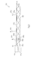
- Figure 3 is a cross-sectional view of an out-coupling layer (or apparatus) 300 which can be used in a backlight layer structure of Figures 1 and 2 to separately couple out the red, green and blue lights from the medium at predetermined positions.
- the apparatus 300 is equivalent to layers 14b and 14c of Figure 2 .
- the apparatus 300 comprises a waveguide 305 with out-coupling diffraction gratings 303a, 303b and 303c for red (wavelength 630 nm), green (wavelength 530 nm) and blue light (wavelength 460 nm), respectively.
- the diffraction gratings may for instance be embossed on the surface of a waveguide 305 or otherwise formed in or attached to the surface of waveguide 305. Therein, directly forming the diffraction gratings on the surface of waveguide 305 yields a particularly cost-efficient structure.
- the waveguide 305 receives red light 302a from a light source 301a, green light 302b from a light source 301b and blue light 302c from a light source 301c.
- the light sources 301a, 301b and 301c may for instance be Light Emitting Diodes (LEDs) or lasers, such as for instance semiconductor, frequency-doubled or pumped solid-state lasers.
- LEDs Light Emitting Diodes
- lasers such as for instance semiconductor, frequency-doubled or pumped solid-state lasers.
- the red light 302a and the blue light 302c are received in the waveguide 305 in orthogonal direction with respect to the green light 302b, i.e., the red light 302a and the blue light 302c are received in a direction that is parallel to the plane in which the cross-sectional view of Figure 3 is lying, and the green light 302b is received in a direction that is parallel to the normal vector of the plane and that is illustrated as an "X" within a circle.
- each light field is assumed to propagate inside the waveguide 305 at a range of angles that supports total internal reflection, i.e., the red light 302a, the green light 302b and the blue light 302c are reflected from top and bottom surfaces of the waveguide 305 thus supporting guided mode propagation.
- red light 304a, green light 304b and blue light 304c are coupled out of waveguide 305.
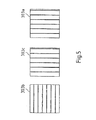
- the orientation of the out-coupling gratings 303a, 303b and 303c is depicted in Figure 5 . It is readily visible that the diffraction grating 303a for red light and the diffraction grating for blue light 303c have the same orientation, whereas the diffraction grating 303b for green light has an orthogonal orientation.
- Figure 4 shows more detailed cross-sectional views of the waveguide 305 of apparatus 300 according to Figure 3 for transmissive out-coupling. Therein, reference numbers already used in Fig. 3 are maintained. Furthermore, the orientation of the diffraction gratings 303a, 303b and 303c as illustrated in Figure 5 also applies to Figure 4 .
- the waveguide 305 according to Figure 4 consists of a substrate 305-1 (which corresponds to the grating layer 14a in Figure 2 ) and a coating layer 305-2 (which corresponds to the waveguide 14b in Figure 2 ).
- the output coupling grating 303c for blue light 302c is formed on the waveguide substrate 305-2, while the output coupling grating 303b for green light 302b (illustrated as an "X" within a circle) and the output coupling grating 303a for red light 302a are formed on top of the coating layer 305-2.
- the refractive index of the coating layer 305-2 is selected to be smaller than that of the substrate 305-1, and the incidence angle of blue light 302c is chosen high enough to support total internal reflection of blue light at the interface between substrate 305-1 and coating layer 305-2. This effectively isolates the blue light 302c from the diffraction gratings 303a and 303b for the red and green lights thus enabling output coupling of blue light 302c to be obtained from diffraction grating 303c only.
- the thickness of the coating layer 305-2 is selected to be small enough to enable decoupling of out-coupled blue light 304c from the diffraction gratings 303a and 303b for the red and green lights.
- the grating period of diffraction grating 303c is selected to be small enough to function as an effective index medium for long wavelength (red) light.
- the grating 303c for blue light does not support any diffracted modes for red light, thus preventing the red light 302a from being coupled out of the waveguide by the diffraction grating 303c for the blue light.
- the green light 302b is coupled into the waveguide 305 in an orthogonal direction with respect to the blue light 302c. Since the green light 302b is now propagating in parallel to the groove direction of the diffraction grating 303c for blue light (see Figure 5 ), it is effectively not coupled out by the diffraction grating 303c.
- the output coupling gratings 303b and 303a for green and red lights are formed on top of the coating layer 305-2, and the incidence angles of the respective light are selected to be small enough to enable propagation through the interface between the substrate 305-1 and the coating layer 305-2, but high enough to support total internal reflection at the interface between the coating layer 305-2 and the medium adjoining to the coating layer 305-2, for instance air (in Figure 2 , this interface is determined by the cladding layer 14c).
- the groove direction of the grating 303b for green light is selected to be orthogonal with respect to the groove direction of the gratings 303a and 303c for the red and blue lights. This enables the green light 302b to be coupled out of the waveguide 305 using the diffraction grating 303b, while the red light 302a is not affected by it.
- the orthogonal groove direction decouples the green light 302b from interaction with the diffraction grating 303a for the red light.
- the grating configuration as described above enables the blue light 302c, the green light 302b and the red light 302a to be coupled out of the waveguide 305 by the gratings 303c for the blue light, 303b for the green light and 303a for the red light, respectively, yielding out-coupled blue light 304c, out-coupled green light 304b and out-coupled red light 304a.
- Cross talk of the output coupling is effectively eliminated with the use of the coating layer 305-2 and crossed grating configurations.
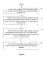
- Figure 6 shows an example of a flow chart for using a display structure with integrated backlighting, according to an embodiment of the present invention.
- a plurality of lights of primary colors e.g., red, blue, green
- a first substrate e.g., comprising electrically conducting layer
- the portions of each of said plurality of lights of different colors are diffractively out-coupled to pre-selected pixels comprising conductive electrodes and, e.g., located on the second substrate using one or more optical layers of the first substrate.
- a next step 34 the portions of each of said plurality of lights of different colors are light modulated in predetermined areas of the modulation layer corresponding to said pixels by applying electric signals corresponding to data of an image to the pixels for providing electric fields between said pixels and the electrically conducting layer.
- the portions of each of the plurality of lights of different colors are further out-coupled out of the second substrate after being light modulated by the electric fields corresponding to the data of said image for providing said image.
- FIG. 7 shows a schematic representation of an electronic device 100 utilizing a display device with integrated backlighting 230, according to an embodiment of the present invention.
- the display module 230 can be used in the electronic (e.g., portable or non-portable) device 100, such as a mobile phone, a computer, a monitor, a TV set, personal digital assistant (PDA), communicator, portable Internet appliance, digital video and still camera, a computer game device, and other electronic devices utilizing viewing.
- the device 100 has a housing 210 to house a communication unit 212 for possible receiving and transmitting information from and to an external device (not shown).
- the device 100 also has a controlling and processing unit 214 for handling the received and transmitted information.
- the controlling and processing unit 214 is operatively connected to the module 230 to provide image data which is displayed by the module 230 using various embodiments of the present invention described herein.
- an apparatus comprising:
- said first substrate comprises said electrically conducting layer and said second substrate comprises said pixels.
- said first substrate is a planar rigid substrate.
- said one or more optical layers comprises one optical layer with disposed a further plurality of diffraction gratings such that each of said diffraction gratings is configured to provide said diffractive out-coupling for only one color of said different colors, the further plurality being equal to said plurality.
- said one or more optical layers further comprises a cladding layer next to said one optical layer for providing said diffractive out-coupling, wherein index of refraction of said cladding layer is substantially lower than index of refraction of said one optical layer.
- the apparatus wherein said plurality of lights are red, green and blue.
- said at least one optical layer is configured to provide said launching said plurality of lights using at least one of: prism coupling, edge coupling, grating coupling and butt coupling.
- said modulation layer is a liquid crystal and said light modulation is provided for varying a state of optical polarization of said portions of each of said plurality of lights of different colors.
- the apparatus further comprises a polarization layer configured to provide, after said varying the state of optical polarization, said light intensity modulation of said portions of each of said plurality of lights of different colors for said further out-coupling from the second substrate, wherein said polarization layer is disposed on said second substrate or said polarization layer is a separate layer next to said second substrate.
- said at least one optical layer is made of a birefringent material or said first substrate further comprises a birefringent layer next to said at least one optical layer for redistributing optical polarization states of said plurality of lights of different colors to increase efficiency of said out-coupling.
- first substrate or said first and second substrates are made of substantially non-absorbing optical materials.
- modulation layer is an electro-wetting material.
- each said pixels comprise a conductive electrode and a thin-film transistor structure for applying said electric signals.
- said electrically conducting layer and said conductive electrodes are made of indium tin oxide.
- said electrically conducting layer is a wiregrid polarizer.
- the apparatus further comprises a corresponding color filter next to each of said pixels to further provide intended spectral content of said portions of each of said plurality of lights of different colors.
- a method comprising:
- said display device is a liquid crystal display, an electro-wetting display, a microelectromechanical system display or an electrophoretic display.
- said first substrate comprises said electrically conducting layer and said second substrate comprises said pixels.
- said one or more optical layers comprises one optical layer with disposed a further plurality of diffraction gratings such that each of said diffraction gratings is configured to provide said out-coupling for only one color of said different colors, the further plurality being equal to said plurality.
- said one or more optical layers further comprises a cladding layer next to said one optical layer for providing said diffractive out-coupling, wherein index of refraction of said cladding layer is substantially lower than index of refraction of said one optical layer.
- said at least one optical layer is made of a birefringent material or said first substrate further comprises a birefringent layer next to said at least one optical layer for redistributing optical polarization states of said plurality of lights of different colors to increase efficiency of said out-coupling.
- nn electronic device comprising:
- said one or more optical layers comprises one optical layer with disposed a further plurality of diffraction gratings such that each of said diffraction gratings is configured to provide said out-coupling for only one color of said different colors, the further plurality being equal to said plurality.
- an apparatus comprising: first means for light propagation; second means for light propagation; and means for modulation between said first and second means for light propagation, wherein light modulation in predetermined areas of said means for modulation corresponding to pixels comprising conductive electrodes and located on the first or the second means for light propagation is provided by applying electric signals corresponding to data of an image to said pixels for providing electric fields between said pixels and an electrically conducting layer of an opposite means for light propagation, the first or the second means for light propagation, wherein said first means for light propagation comprises at least one optical layer configured to provide launching of a plurality of lights of different colors and further comprises one or more optical layers configured to provide diffractive out-coupling of portions of each of said plurality of lights of different colors to preselected pixels or subpixels of said pixels separately from other colors of said different colors, wherein said second means for light propagation is configured to provide further out-coupling of said portions of each of said plurality of lights of different colors
- said first means for light propagation is a first substrate
- said second means for light propagation is a second substrate
- said means for modulation is a modulation layer
Landscapes
- Physics & Mathematics (AREA)
- General Physics & Mathematics (AREA)
- Optics & Photonics (AREA)
- Nonlinear Science (AREA)
- Engineering & Computer Science (AREA)
- Microelectronics & Electronic Packaging (AREA)
- Mathematical Physics (AREA)
- Chemical & Material Sciences (AREA)
- Crystallography & Structural Chemistry (AREA)
- Liquid Crystal (AREA)
Abstract
Description
- The present invention relates generally to electronic devices comprising displays and, more specifically, to display device structures with integrated backlighting utilizing separate color coupling.
- In a present state of technology a liquid crystal display (LCD) is essentially a stack of optical films and glass, having been developed as a series of improvements over a legacy platform of the flat panel display. The basic structure of an active-matrix LCD incorporates a thin-film transistor backplane that defines the pixel structure of the display. A backlight is used to launch light through the pixel structure. Currently, white light is essentially uniformly spread on the pixel array, where part of it is blocked by the transistor structure, and the rest is filtered through the pixel (or subpixel) color filters typically to red, green, and blue light. Then the liquid crystal (LC) is used to modulate the intensity of the light passing through the pixel. It is evident that a lot of light is wasted in the absorption of unwanted light, and the resulting structure is unnecessarily thick due to stacking of films. In the present state of technology the backlight structure is usually implemented as a separate panel/structure from the display panel substrate comprising the thin-film transistor backplane.
- According to a first aspect of the invention, an apparatus, comprises: a first substrate; a second substrate; and a modulation layer between the first and second substrates, wherein light modulation in predetermined areas of the modulation layer corresponding to pixels comprising conductive electrodes and located on the first or the second substrate is provided by applying electric signals corresponding to data of an image to the pixels for providing electric fields between the pixels and an electrically conducting layer of an opposite substrate, the first or the second substrate, wherein the first substrate comprises at least one optical layer configured to provide launching of a plurality of lights of different colors and further comprises one or more optical layers configured to provide diffractive out-coupling of portions of each of the plurality of lights of different colors to pre-selected pixels or subpixels of the pixels separately from other colors of the different colors, wherein the second substrate is configured to provide further out-coupling of the portions of each of the plurality of lights of different colors after being light modulated by the electric fields corresponding to the data of the image for providing the image.
- According further to the first aspect of the invention, the first substrate may comprise the electrically conducting layer and the second substrate may comprise the pixels.
- Further according to the first aspect of the invention, the first substrate may be a planar rigid substrate.
- Still further according to the first aspect of the invention, the one or more optical layers may comprise one optical layer with disposed a further plurality of diffraction gratings such that each of the diffraction gratings may be configured to provide the diffractive out-coupling for only one color of the different colors, the further plurality being equal to the plurality. Still further, the one or more optical layers may further comprise a cladding layer next to the one optical layer for providing the diffractive out-coupling, wherein index of refraction of the cladding layer is substantially lower than index of refraction of the one optical layer. Yet still further, at least one of the further plurality of diffraction gratings may be a slanted grating.
- According further to the first aspect of the invention, the plurality of lights may be red, green and blue.
- According still further to the first aspect of the invention, the at least one optical layer may be configured to provide the launching the plurality of lights using at least one of: prism coupling, edge coupling, grating coupling and butt coupling.
- According yet still further to the first aspect of the invention, portions of each of the plurality of lights of different colors may have a predetermined optical polarization.
- According further still to the first aspect of the invention, the modulation layer may be a liquid crystal and the light modulation may be provided for varying a state of optical polarization of the portions of each of the plurality of lights of different colors. Still further, the apparatus may further comprise a polarization layer configured to provide, after the varying the state of optical polarization, the light intensity modulation of the portions of each of the plurality of lights of different colors for the further out-coupling from the second substrate, wherein the polarization layer is disposed on the second substrate or the polarization layer is a separate layer next to the second substrate.
- Yet still further according to the first aspect of the invention, the at least one optical layer may be made of a birefringent material or the first substrate may further comprise a birefringent layer next to the at least one optical layer for redistributing optical polarization states of the plurality of lights of different colors to increase efficiency of the out-coupling.
- Still yet further according to the first aspect of the invention, the first substrate or the first and second substrates may be made of substantially non-absorbing optical materials.
- Still further still according to the first aspect of the invention, the modulation layer may be an electro-wetting material.
- According further to the first aspect of the invention, each of the pixels may comprise a conductive electrode and a thin-film transistor structure for applying the electric signals.
- Further according to the first aspect of the invention, the electrically conducting layer and the conductive electrodes may be made of indium tin oxide.
- Still further according to the first aspect of the invention, the electrically conducting layer may be a wiregrid polarizer.
- According further to the first aspect of the invention, the apparatus may further comprise a corresponding color filter next to each of the pixels to further provide intended spectral content of the portions of each of the plurality of lights of different colors.
- According to a second aspect of the invention, a method, comprises: launching a plurality of lights of different colors to at least one optical layer of a first substrate; diffractively out-coupling portions of each of the plurality of lights of different colors to pre-selected pixels or subpixels of pixels comprising conductive electrodes and located on the first or a second substrate using one or more optical layers of the first substrate; light modulating portions of each of the plurality of lights of different colors in predetermined areas of a modulation layer corresponding to the pixels by applying electric signals corresponding to data of an image to the pixels for providing electric fields between the pixels and an electrically conducting layer of an opposite substrate, the first or the second substrate, wherein the modulation layer is between the first and second substrates; and further out-coupling the portions of each of the plurality of lights of different colors out of the second substrate after being light modulated by the electric fields corresponding to the data of the image for providing the image.
- According further to the second aspect of the invention, the first substrate, the second substrate and the modulation layer may be parts of a display device. Still further, the display device may be a liquid crystal display, an electro-wetting display, a microelectromechanical system display or an electrophoretic display.
- Further according to the second aspect of the invention, the launching of the plurality of lights of different colors may be provided by light emitting diodes.
- Still further according to the second aspect of the invention, the first substrate may comprise the electrically conducting layer and the second substrate may comprise the pixels.
- Yet still further according to the second aspect of the invention, the one or more optical layers may comprise one optical layer with disposed a further plurality of diffraction gratings such that each of the diffraction gratings is configured to provide the out-coupling for only one color of the different colors, the further plurality being equal to the plurality. Still further, the one or more optical layers may further comprise a cladding layer next to the one optical layer for providing the diffractive out-coupling, wherein index of refraction of the cladding layer is substantially lower than index of refraction of the one optical layer. Yet still further, at least one of the further plurality of diffraction gratings may be a slanted grating.
- According still further to the second aspect of the invention, the at least one optical layer may be made of a birefringent material or the first substrate further may comprise a birefringent layer next to the at least one optical layer for redistributing optical polarization states of the plurality of lights of different colors to increase efficiency of the out-coupling.
- According to a third aspect of the invention, an electronic device, comprises:
- a data processing unit;
- an optical engine operatively connected to the data processing unit for receiving data of an image from the data processing unit;
- a display device with integrated backlighting operatively connected to the optical engine for forming the image based on the data, comprising: a first substrate; a second substrate; and a modulation layer between the first and second substrates, wherein light modulation in predetermined areas of the modulation layer corresponding to pixels comprising conductive electrodes and located on the first or the second substrate is provided by applying electric signals corresponding to data of an image to the pixels for providing electric fields between the pixels and an electrically conducting layer of an opposite substrate, the first or the second substrate, wherein the first substrate comprises at least one optical layer configured to provide launching of a plurality of lights of different colors and further comprises one or more optical layers configured to provide diffractive out-coupling of portions of each of the plurality of lights of different colors to pre-selected pixels or subpixels of the pixels separately from other colors of the different colors, wherein the second substrate is configured to provide further out-coupling of the portions of each of the plurality of lights of different colors after being light modulated by the electric fields corresponding to the data of the image for providing the image.
- According further to the third aspect of the invention, the one or more optical layers may comprise one optical layer with disposed a further plurality of diffraction gratings such that each of the diffraction gratings may be configured to provide the out-coupling for only one color of the different colors, the further plurality being equal to the plurality.
- According to a fourth aspect of the invention, an apparatus, comprises: first means for light propagation; second means for light propagation; and means for modulation between the first and second means for light propagation, wherein light modulation in predetermined areas of the means for modulation corresponding to pixels comprising conductive electrodes and located on the first or the second means for light propagation is provided by applying electric signals corresponding to data of an image to the pixels for providing electric fields between the pixels and an electrically conducting layer of an opposite means for light propagation, the first or the second means for light propagation, wherein the first means for light propagation comprises at least one optical layer configured to provide launching of a plurality of lights of different colors and further comprises one or more optical layers configured to provide diffractive out-coupling of portions of each of the plurality of lights of different colors to pre-selected pixels or subpixels of the pixels separately from other colors of the different colors, wherein the second means for light propagation is configured to provide further out-coupling of the portions of each of the plurality of lights of different colors after being light modulated by the electric fields corresponding to the data of the image for providing the image.
- According further to the fourth aspect of the invention, the first means for light propagation may be a first substrate, the second means for light propagation may be a second substrate and the means for modulation may be a modulation layer.
- For a better understanding of the nature and objects of the present invention, reference is made to the following detailed description taken in conjunction with the following drawings, in which:
-
Figure 1 is a schematic representation of a display structure with integrated backlighting, according to an embodiment of the present invention; -
Figure 2 is a schematic representation for a specific implementation of a liquid crystal display structure with integrated backlighting, according to an exemplary embodiment of the present invention; -
Figure 3 is a cross-sectional view of an out-coupling layer which can be used in a backlight layer structure ofFigures 1 and2 ; -
Figure 4 is a more detailed cross-sectional view of an out-coupling layer structure shown inFigure 3 for transmissive out-coupling; -
Figure 5 is a schematic representation illustrating the orientation of the out-coupling diffraction gratings of the out-coupling module shown inFigures 3 and4 . -
Figure 6 is a flow chart for using a display structure with integrated backlighting, according to an embodiment of the present invention; and -
Figure 7 is a schematic representation of an electronic device utilizing a display structure with integrated backlighting, according to an embodiment of the present invention. - A new apparatus and method are provided for designing and using display devices with integrated backlight layer structures utilizing separate color diffractive out-coupling (e.g., diffraction out-coupling). According to embodiments of the present invention, a lower substrate of the display can be used to integrate the backlight component (or the backlight layer structure), thus enabling a thin module with the integrated backlighting. The display devices can be (but are not limited to): liquid crystal displays (LCDs), electro-wetting displays, microelectromechanical system (MEMS) displays, electrophoretic displays, etc. The diffractive optics principles of the
PCT application 061327WO filed on November 17, 2006 - According to an embodiment of the present invention, the apparatus (e.g., the display device) can comprise: a first (e.g., a lower substrate) substrate, a second substrate (e.g., an upper substrate); and a modulation layer between the first and second substrates, wherein light modulation in predetermined areas of the modulation layer corresponding to pixels of conducting material (i.e., conductive electrodes) located on the first or the second substrate is provided by applying electric signals corresponding to data of an image to said pixels for providing electric fields between the pixels and an electrically conducting layer (e.g., optically transparent indium tin oxide, ITO) of an opposite substrate, the first or the second substrate, and wherein the first substrate comprises at least one optical layer configured to provide launching of a plurality of lights of different colors and further comprises one or more optical layers configured to provide out-coupling (e.g., using diffraction gratings) of portions of each of the plurality of lights of different colors to pre-selected pixels or subpixels of said pixels (i.e., all display pixels) separately from other colors of the different colors, wherein said second substrate is configured to further out-couple the portions of each of the plurality of lights of different colors after being light modulated by said electric fields corresponding to said data of the image for providing said image. If the modulation layer is a liquid crystal (used in LCDs), then the light modulation is provided for varying a state of optical polarization of the portions of each of said plurality of lights of different colors (typically each of said plurality of lights of different colors has a predetermined optical polarization), and a polarization layer (e.g., disposed on the second substrate or a separate layer next to the second substrate) is configured to provide, after said varying the state of optical polarization, the light intensity modulation of said portions of each of the plurality of lights of different colors for out-coupling from the second substrate.
- It is noted that the pixel defines the resolution of the display and is the smallest element (area) comprising averaged brightness and color information of that element. In the context of this invention the subpixel is a part of the pixel, and comprises one color defining the brightness of that color.
- Moreover, the one or more optical layers, described herein, can comprise one optical layer with a number (e.g., equal to the plurality of lights) of diffraction gratings or grating arrays disposed on it such that each of the diffraction gratings is configured to provide the out-coupling for only one color of the different colors. Furthermore, the one or more optical layers can further comprise a cladding layer next to said one optical layer for providing the diffractive out-coupling, wherein the index of refraction of the cladding layer is substantially lower than the index of refraction of said one optical layer. Also, using diffractive slanted gratings (e.g., see T. Levola, P. Laakkonen "Replicated Slanted Gratings with a High Refractive Index Material for in and Outcoupling of Light", Optics Express, vol. 15, No.5, pages 2067-2074) can provide an improvement in the out-coupling efficiency of the diffraction gratings. It is further noted that a corresponding color filter next to each of the pixels can be used to further provide intended spectral content of said portions of each of the plurality of lights of different colors.
- In one further embodiment, the display structure can be an inverted thin-film transistor based display structure such as LCD, where the transistor layer (e.g., implemented as thin-film transistor (TFT) layer), identifying pixels, is on the upper substrate of the display, whereas the lower substrate of the display is used to integrate the backlight component and the electrically conducting layer (for applying the electric signals corresponding to the data of an image), as described herein, thus using this backlight component as close as possible to the LC (liquid crystal) layer in order to have maximum control of the diffracted (out-coupled) light. However, in general, the pixels can be located on the lower substrate integrated with the backlight component and the electrically conducting layer can be located on the opposite (upper) substrate. Each pixel can comprise a conductive electrode (e.g., made of ITO) and a thin-film transistor (TFT) structure for applying the electric signals corresponding to the data.
- According to various embodiments, a variety of different types of substrate (e.g., glass, polymer, planar, rigid, flexible, etc.) and displays with multiple primary colors (e.g., two, three or more) can be used. Also the light can be launched into the lower substrate of the display by using prism, edge, grating, butt coupling, etc. The launching of the plurality of lights of different colors can be provided by light emitting diodes (LEDs), lasers, CCFL (cold cathode fluorescent light) micro lamps, CNT (cathodoluminescent) light sources, etc.
- The substrate can include a launch/fan-out structure that can distribute the launched light along the edge area of the display. For example, one color can be coupled in from its respective corner or corners, and other primary colors respectively from their own corners. All primaries can have their own launch/fanout areas that are designed to provide a uniform distribution of light into the substrate. Light then can travel in the substrate relatively freely, e.g., due to total internal reflection by controlling launch angles at the launch/fanout area. If the inverted structure is used, the transistor TFT structure would not interfere with the propagation of light in the lower substrate at all.
- The embodiments of the present invention describing the integrated structure can provide significant savings in light throughput efficiency which will result in brighter displays, can create savings in power consumption of the display, may result in a better color gamut, and can enable a much thinner component to be manufactured.
-
Figure 1 shows an example among others of a schematic representation of adisplay structure 10 with integrated backlighting, according to an embodiment of the present invention. Thestructure 10 comprises alower substrate 12, amodulation layer 18 and anupper substrate 20. Thelower substrate 12 comprises abacklight layer structure 14, as described herein, integrated with standard layers, e.g., electrically conducting layer, alignment layer for a liquid crystal in the LCDs, etc., according to various embodiments of the present invention. Themodulation layer 18 could be a liquid crystal, electro-wetting material, a MEMS structure, etc. Theupper substrate 20 typically comprises standard layers, e.g., pixels comprising transistor (TFT) and electrode (e.g., ITO) layers, an alignment layer for a liquid crystal in the LCDs, polarization and diffuser layers (e.g., for LCDs). It is noted that polarization and diffuser layers could be disposed on the upper substrate or could be separate layers (foils) next to the upper substrate. It is noted that thesubstrates - It is noted that the
lower substrate 12 can generally be means for light propagation or a structural equivalence (or an equivalent structure) thereof. Similarly, theupper substrate 20 can generally be means for light propagation or a structural equivalence (or equivalent structure) thereof. Also, themodulation layer 18 can generally be means for modulation or a structural equivalence (or equivalent structure) thereof. -
Figure 2 shows another example among others of a schematic representation for a specific implementation of a liquid crystal display (LCD)structure 10a with integrated backlighting, according to an exemplary embodiment of the present invention. - The
backlight layer structure 14 comprises alightguide 14a for launching lights of different colors (e.g., red, blue and green) which are separately out-coupled by thegrating layer 14b, as shown inFigure 2 , to correspondingpixels upper substrate 20. Furthermore, thebacklight layer structure 14 can comprise a cladding layer14c next to thegrating layer 14b for providing effective diffractive out-coupling by thegrating layer 14b, wherein the index of refraction of thecladding layer 14c is substantially lower than the index of refraction of thegrating layer 14b. Moreover, thebacklight layer structure 14 can further comprise abirefringent layer 14d next to thelightguide 14a for redistributing optical polarization states of the plurality of lights (e.g., red, blue and green) launched to thelightguide 14a for increasing efficiency of the diffractive out-coupling. Thebirefringent layer 14d may not be needed if at least thelightguide 14a and possibly other layers of thebacklight layer structure 14 are made of a birefringent material. - The standard layers 16 of the
lower substrate 12 can comprise an electrically conducting layer (e.g., made of ITO) 16a for providing an electrical contact to perform light modulation, and analignment layer 16b to support operation of a liquid crystal (LC)layer 18a (with spacers as standard technology). It is further noted that a polarizer layer can be functionally a part of thelayer 16a, e.g., a wiregrid polarizer can be simultaneously an electrode (for providing said electrical contact to perform light modulation) and a polarizer. This wiregrid polarizer can also perform a function of analignment layer 16b. Theupper substrate 20 can comprise anotheralignment layer 20a to support operation of aliquid crystal layer 18a, and an array ofpixels conductive electrode layer 20b (e.g., made of ITO) and a thin-film transistor (TFT)layer 20c for applying the electric signals corresponding to the image data. It is noted that the pixels can also have an additional color filter (not shown inFigure 2 ) to provide the desired spectral purity of the lights of different colors diffractively out-coupled by thegrating layer 14b. Finally, polarization anddiffuser layers upper substrate 20 or provided as separate layers (foils) next to theupper substrate 20. - It is noted that the example of
Figure 2 demonstrates launching lights of different colors (e.g., red, blue and green) to correspondingpixels - As it is stated herein, the diffractive optics principles of the
PCT application 061327WO filed on November 17, 2006 PCT application 061327WO Figures 3-5 . -
Figure 3 is a cross-sectional view of an out-coupling layer (or apparatus) 300 which can be used in a backlight layer structure ofFigures 1 and2 to separately couple out the red, green and blue lights from the medium at predetermined positions. Theapparatus 300 is equivalent tolayers Figure 2 . - The
apparatus 300 comprises awaveguide 305 with out-coupling diffraction gratings waveguide 305 or otherwise formed in or attached to the surface ofwaveguide 305. Therein, directly forming the diffraction gratings on the surface ofwaveguide 305 yields a particularly cost-efficient structure. Via an interface, e.g., the air-waveguide interface (inFigure 2 , this interface is determined by thecladding layer 14c), thewaveguide 305 receivesred light 302a from alight source 301a,green light 302b from alight source 301b and blue light 302c from alight source 301c. Therein, thelight sources red light 302a and theblue light 302c are received in thewaveguide 305 in orthogonal direction with respect to thegreen light 302b, i.e., thered light 302a and theblue light 302c are received in a direction that is parallel to the plane in which the cross-sectional view ofFigure 3 is lying, and thegreen light 302b is received in a direction that is parallel to the normal vector of the plane and that is illustrated as an "X" within a circle. - Therein, each light field is assumed to propagate inside the
waveguide 305 at a range of angles that supports total internal reflection, i.e., thered light 302a, thegreen light 302b and theblue light 302c are reflected from top and bottom surfaces of thewaveguide 305 thus supporting guided mode propagation. - Via the out-
coupling diffraction gratings 303a for red light, 303b for green light and 303c for blue light,red light 304a,green light 304b andblue light 304c are coupled out ofwaveguide 305. The orientation of the out-coupling gratings Figure 5 . It is readily visible that thediffraction grating 303a for red light and the diffraction grating forblue light 303c have the same orientation, whereas thediffraction grating 303b for green light has an orthogonal orientation. -
Figure 4 shows more detailed cross-sectional views of thewaveguide 305 ofapparatus 300 according toFigure 3 for transmissive out-coupling. Therein, reference numbers already used inFig. 3 are maintained. Furthermore, the orientation of thediffraction gratings Figure 5 also applies toFigure 4 . Thewaveguide 305 according toFigure 4 consists of a substrate 305-1 (which corresponds to thegrating layer 14a inFigure 2 ) and a coating layer 305-2 (which corresponds to thewaveguide 14b inFigure 2 ). The output coupling grating 303c forblue light 302c is formed on the waveguide substrate 305-2, while the output coupling grating 303b forgreen light 302b (illustrated as an "X" within a circle) and the output coupling grating 303a forred light 302a are formed on top of the coating layer 305-2. - The refractive index of the coating layer 305-2 is selected to be smaller than that of the substrate 305-1, and the incidence angle of
blue light 302c is chosen high enough to support total internal reflection of blue light at the interface between substrate 305-1 and coating layer 305-2. This effectively isolates theblue light 302c from thediffraction gratings diffraction grating 303c only. Moreover, the thickness of the coating layer 305-2 is selected to be small enough to enable decoupling of out-coupled blue light 304c from thediffraction gratings - To prevent output coupling of red light from the
diffraction grating 303c intended for blue light, the grating period ofdiffraction grating 303c is selected to be small enough to function as an effective index medium for long wavelength (red) light. In other words, the grating 303c for blue light does not support any diffracted modes for red light, thus preventing thered light 302a from being coupled out of the waveguide by thediffraction grating 303c for the blue light. - To prevent green light from being output coupled by the
diffraction grating 303c intended for blue light, thegreen light 302b is coupled into thewaveguide 305 in an orthogonal direction with respect to theblue light 302c. Since thegreen light 302b is now propagating in parallel to the groove direction of thediffraction grating 303c for blue light (seeFigure 5 ), it is effectively not coupled out by thediffraction grating 303c. - The
output coupling gratings Figure 2 , this interface is determined by thecladding layer 14c). - As depicted in
Figure 5 , the groove direction of the grating 303b for green light is selected to be orthogonal with respect to the groove direction of thegratings green light 302b to be coupled out of thewaveguide 305 using thediffraction grating 303b, while thered light 302a is not affected by it. On the other hand, the orthogonal groove direction decouples thegreen light 302b from interaction with thediffraction grating 303a for the red light. - The grating configuration as described above enables the
blue light 302c, thegreen light 302b and thered light 302a to be coupled out of thewaveguide 305 by thegratings 303c for the blue light, 303b for the green light and 303a for the red light, respectively, yielding out-coupledblue light 304c, out-coupledgreen light 304b and out-coupledred light 304a. Cross talk of the output coupling is effectively eliminated with the use of the coating layer 305-2 and crossed grating configurations. - Also using diffractive slanted gratings (e.g., see T. Levola, P. Laakkonen "Replicated Slanted Gratings with a High Refractive Index Material for in and Outcoupling of Light", Optics Express, vol. 15, No.5, pages 2067-2074) in
Figures 3-5 can provide improvement in the out-coupling efficiency of the backlight layer structure. -
Figure 6 shows an example of a flow chart for using a display structure with integrated backlighting, according to an embodiment of the present invention. - The flow chart of
Figure 6 only represents one possible scenario among others. It is noted that the order of steps shown inFigure 6 is not absolutely required, so in principle, the various steps can be performed out of order. In a method according to the embodiment of the present invention, in afirst step 30, a plurality of lights of primary colors (e.g., red, blue, green) are launched to at least one optical layer of a first substrate, e.g., comprising electrically conducting layer. In anext step 32, the portions of each of said plurality of lights of different colors are diffractively out-coupled to pre-selected pixels comprising conductive electrodes and, e.g., located on the second substrate using one or more optical layers of the first substrate. In anext step 34, the portions of each of said plurality of lights of different colors are light modulated in predetermined areas of the modulation layer corresponding to said pixels by applying electric signals corresponding to data of an image to the pixels for providing electric fields between said pixels and the electrically conducting layer. In anext step 36, the portions of each of the plurality of lights of different colors are further out-coupled out of the second substrate after being light modulated by the electric fields corresponding to the data of said image for providing said image. -
Figure 7 shows a schematic representation of anelectronic device 100 utilizing a display device withintegrated backlighting 230, according to an embodiment of the present invention. Thedisplay module 230 can be used in the electronic (e.g., portable or non-portable)device 100, such as a mobile phone, a computer, a monitor, a TV set, personal digital assistant (PDA), communicator, portable Internet appliance, digital video and still camera, a computer game device, and other electronic devices utilizing viewing. As shown inFigure 7 , thedevice 100 has ahousing 210 to house acommunication unit 212 for possible receiving and transmitting information from and to an external device (not shown). Thedevice 100 also has a controlling andprocessing unit 214 for handling the received and transmitted information. The controlling andprocessing unit 214 is operatively connected to themodule 230 to provide image data which is displayed by themodule 230 using various embodiments of the present invention described herein. - It is noted that various embodiments of the present invention recited herein can be used separately, combined or selectively combined for specific applications.
- It is to be understood that the above-described arrangements are only illustrative of the application of the principles of the present invention. Numerous modifications and alternative arrangements may be devised by those skilled in the art without departing from the scope of the present invention, and the appended claims are intended to cover such modifications and arrangements.
- According to some, but not necessarily all embodiments of the invention, there is provided, an apparatus, comprising:
- a first substrate;
- a second substrate; and
- a modulation layer between said first and second substrates, wherein light modulation in predetermined areas of said modulation layer corresponding to pixels comprising conductive electrodes and located on the first or the second substrate is provided by applying electric signals corresponding to data of an image to said pixels for providing electric fields between said pixels and an electrically conducting layer of an opposite substrate, the first or the second substrate,
- wherein said first substrate comprises at least one optical layer configured to provide launching of a plurality of lights of different colors and further comprises one or more optical layers configured to provide diffractive out-coupling of portions of each of said plurality of lights of different colors to pre-selected pixels or subpixels of said pixels separately from other colors of said different colors, wherein said second substrate is configured to provide further out-coupling of said portions of each of said plurality of lights of different colors after being light modulated by said electric fields corresponding to said data of said image for providing said image.
- The apparatus, wherein said first substrate comprises said electrically conducting layer and said second substrate comprises said pixels.
- The apparatus, wherein said first substrate is a planar rigid substrate.
- The apparatus, wherein said one or more optical layers comprises one optical layer with disposed a further plurality of diffraction gratings such that each of said diffraction gratings is configured to provide said diffractive out-coupling for only one color of said different colors, the further plurality being equal to said plurality.
- The apparatus, wherein said one or more optical layers further comprises a cladding layer next to said one optical layer for providing said diffractive out-coupling, wherein index of refraction of said cladding layer is substantially lower than index of refraction of said one optical layer.
- The apparatus, wherein at least one of said further plurality of diffraction gratings is a slanted grating.
- The apparatus, wherein said plurality of lights are red, green and blue.
- The apparatus, wherein said at least one optical layer is configured to provide said launching said plurality of lights using at least one of: prism coupling, edge coupling, grating coupling and butt coupling.
- The apparatus, wherein portions of each of said plurality of lights of different colors has a predetermined optical polarization.
- The apparatus, wherein said modulation layer is a liquid crystal and said light modulation is provided for varying a state of optical polarization of said portions of each of said plurality of lights of different colors.
- The apparatus, further comprises a polarization layer configured to provide, after said varying the state of optical polarization, said light intensity modulation of said portions of each of said plurality of lights of different colors for said further out-coupling from the second substrate, wherein said polarization layer is disposed on said second substrate or said polarization layer is a separate layer next to said second substrate.
- The apparatus, wherein said at least one optical layer is made of a birefringent material or said first substrate further comprises a birefringent layer next to said at least one optical layer for redistributing optical polarization states of said plurality of lights of different colors to increase efficiency of said out-coupling.
- The apparatus, wherein said first substrate or said first and second substrates are made of substantially non-absorbing optical materials.
- The apparatus, wherein said modulation layer is an electro-wetting material.
- The apparatus, wherein each said pixels comprise a conductive electrode and a thin-film transistor structure for applying said electric signals.
- The apparatus, wherein said electrically conducting layer and said conductive electrodes are made of indium tin oxide.
- The apparatus, wherein said electrically conducting layer is a wiregrid polarizer.
- The apparatus, further comprises a corresponding color filter next to each of said pixels to further provide intended spectral content of said portions of each of said plurality of lights of different colors.
- According to some, but not necessarily all embodiments of the invention, there is provided, a method, comprising:
- launching a plurality of lights of different colors to at least one optical layer of a first substrate;
- diffractively out-coupling portions of each of said plurality of lights of different colors to pre-selected pixels or subpixels of pixels comprising conductive electrodes and located on the first or a second substrate using one or more optical layers of the first substrate;
- light modulating portions of each of said plurality of lights of different colors in predetermined areas of a modulation layer corresponding to said pixels by applying electric signals corresponding to data of an image to said pixels for providing electric fields between said pixels and an electrically conducting layer of an opposite substrate, the first or the second substrate, wherein said modulation layer is between the first and second substrates; and further out-coupling said portions of each of said plurality of lights of different colors out of said second substrate after being light modulated by said electric fields corresponding to said data of said image for providing said image.
- The method, wherein said first substrate, said second substrate and said modulation layer are parts of a display device.
- The method, wherein said display device is a liquid crystal display, an electro-wetting display, a microelectromechanical system display or an electrophoretic display.
- The method, wherein said launching of the plurality of lights of different colors is provided by light emitting diodes.
- The method, wherein said first substrate comprises said electrically conducting layer and said second substrate comprises said pixels.
- The method, wherein said one or more optical layers comprises one optical layer with disposed a further plurality of diffraction gratings such that each of said diffraction gratings is configured to provide said out-coupling for only one color of said different colors, the further plurality being equal to said plurality.
- The method, wherein said one or more optical layers further comprises a cladding layer next to said one optical layer for providing said diffractive out-coupling, wherein index of refraction of said cladding layer is substantially lower than index of refraction of said one optical layer.
- The method, wherein at least one of said further plurality of diffraction gratings is a slanted grating.
- The method, wherein said at least one optical layer is made of a birefringent material or said first substrate further comprises a birefringent layer next to said at least one optical layer for redistributing optical polarization states of said plurality of lights of different colors to increase efficiency of said out-coupling.
- According to some, but not necessarily all embodiments of the invention, there is provided, nn electronic device, comprising:
- a data processing unit;
- an optical engine operatively connected to the data processing unit for receiving data of an image from the data processing unit;
- a display device with integrated backlighting operatively connected to the optical engine for forming said image based on the data, comprising:
- a first substrate;
- a second substrate; and
- a modulation layer between said first and second substrates, wherein light modulation in predetermined areas of said modulation layer corresponding to pixels comprising conductive electrodes and located on the first or the second substrate is provided by applying electric signals corresponding to data of an image to said pixels for providing electric fields between said pixels and an electrically conducting layer of an opposite substrate, the first or the second substrate,
- wherein said first substrate comprises at least one optical layer configured to provide launching of a plurality of lights of different colors and further comprises one or more optical layers configured to provide diffractive out-coupling of portions of each of said plurality of lights of different colors to pre-selected pixels or subpixels of said pixels separately from other colors of said different colors, wherein said second substrate is configured to provide further out-coupling of said portions of each of said plurality of lights of different colors after being light modulated by said electric fields corresponding to said data of said image for providing said image.
- The electronic device, wherein said one or more optical layers comprises one optical layer with disposed a further plurality of diffraction gratings such that each of said diffraction gratings is configured to provide said out-coupling for only one color of said different colors, the further plurality being equal to said plurality.
- According to some, but not necessarily all embodiments of the invention, there is provided, an apparatus, comprising: first means for light propagation;
second means for light propagation; and
means for modulation between said first and second means for light propagation, wherein light modulation in predetermined areas of said means for modulation corresponding to pixels comprising conductive electrodes and located on the first or the second means for light propagation is provided by applying electric signals corresponding to data of an image to said pixels for providing electric fields between said pixels and an electrically conducting layer of an opposite means for light propagation, the first or the second means for light propagation,
wherein said first means for light propagation comprises at least one optical layer configured to provide launching of a plurality of lights of different colors and further comprises one or more optical layers configured to provide diffractive out-coupling of portions of each of said plurality of lights of different colors to preselected pixels or subpixels of said pixels separately from other colors of said different colors, wherein said second means for light propagation is configured to provide further out-coupling of said portions of each of said plurality of lights of different colors after being light modulated by said electric fields corresponding to said data of said image for providing said image. - The apparatus, wherein said first means for light propagation is a first substrate, said second means for light propagation is a second substrate and said means for modulation is a modulation layer.
Claims (15)
- An apparatus, comprising:a first substrate (12);a second substrate (20); anda modulation layer (18) between said first and second substrates (12, 20), wherein light modulation in predetermined areas of said modulation layer (18) corresponding to pixels (22a, 22b, 22c) comprising conductive electrodes and located on the first or the second substrate (12, 20) is provided by applying electric signals corresponding to data of an image to said pixels (22a, 22b, 22c) for providing electric fields between said conductive electrodes of the first or the second substrate (12, 20) and an electrically conducting layer of an opposite, the second or the first substrate (20, 12),wherein said first substrate (12) is configured to receive and guide light of different colors and comprises a plurality of diffraction gratings (303a, 303b, 303c) having
a first diffraction grating (303a) configured to provide diffractive out-coupling of light of at least a first color (302a) to pre-selected pixels (22a, 22b, 22c) or subpixels of said pixels (22a, 22b, 22c), and
a second diffraction grating (303b) configured to provide diffractive out-coupling of light of at least a second color (302b) to pre-selected pixels (22a, 22b, 22c) or subpixels of said pixels (22a, 22b, 22c), wherein a groove direction of the second diffraction grating (303b) is substantially orthogonal to a groove direction of the first diffraction grating (303a), andwherein said second substrate (20) is configured to provide further out-coupling of said light of different colors after said light being modulated by said electric fields in said modulation layer (18) corresponding to said data of said image for providing said image. - The apparatus of claim 1, wherein said first substrate (12) comprises a first optical layer (14b, 305-1) and a second optical layer (14a, 305-2) and an interface between the first optical layer (14b, 305-1) and the second optical layer (14a, 305-2) is configured to enable light of at least the second color (302a, 302b) to propagate thorough without diffractively out-coupling the light of the second color.
- The apparatus of claim 1 or 2, wherein each of said diffraction gratings (303a, 303b, 303c) is configured to provide said diffractive out-coupling for only one color.
- The apparatus of any preceding claim, wherein said apparatus further comprises a cladding layer (14c) next to an optical layer (14b) of said first substrate (12) for providing said diffractive out-coupling, wherein index of refraction of said cladding layer (14c) is substantially lower than index of refraction of said optical layer of said first substrate (12).
- The apparatus of any preceding claim, wherein at least one of said plurality of diffraction gratings is a slanted grating.
- The apparatus of any preceding claim, wherein said light of different colors has a predetermined optical polarization.
- The apparatus of any preceding claim, wherein said modulation layer (18) is a liquid crystal and said light modulations provided for varying a state of optical polarization of said light of different colors.
- The apparatus of claim 7, wherein said second substrate (20) further comprises a polarization layer (20d) configured to provide, after said varying the state of optical polarization, said light intensity modulation of said light of different colors for said further out-coupling from the second substrate (20).
- The apparatus of any preceding claim, wherein the apparatus further comprises one optical layer made of a birefringent material or said first substrate (12) further comprises a birefringent layer (14d) next to at least one optical layer (14a) for redistributing optical polarization states of said light of different colors to increase efficiency of said out-coupling.
- The apparatus of any preceding claim,
wherein said modulation layer (18) comprises an electro-wetting material, and/or
wherein an electrically conducting layer (16a) in the first substrate (12) is a wiregrid polarizer. - An electronic device, comprising: a data processing unit; an optical engine operatively connected to the data processing unit for receiving data of an image from the data processing unit; a display device with integrated backlighting operatively connected to the optical engine for forming said image based on the data, wherein the display device is configured as the apparatus according to any of claims 1-10.
- A method, comprising:coupling light of different colors to a first substrate (12), wherein the first substrate (12) is configured to receive and guide light of different colors and comprises a first diffraction grating (303a) and a second diffraction grating (303b);using the first diffraction grating (303a) to diffractively out-couple light of at least a first color (302a) to pre-selected pixels (22a, 22b, 22c) or subpixels of said pixels (22a, 22b, 22c);using the second diffraction grating (303b) to diffractively out-couple light of at least a second color (302b) to pre-selected pixels (22a, 22b, 22c) or subpixels of said pixels (22a, 22b, 22c), wherein a groove direction of the second diffraction grating (303b) is substantially orthogonal to a groove direction of the first diffraction grating (303a), and wherein said pixels (22a, 22b, 22c) comprising conductive electrodes and located on the first or a second substrate;modulating portions of each of said light of different colors in predetermined areas of a modulation layer (18) corresponding to said pixels (22a, 22b, 22c) by applying electric signals corresponding to data of an image to said pixels (22a, 22b, 22c) for providing electric fields between said conductive electrodes located on the first or the second substrate (12, 20) and an electrically conducting layer of an opposite, the second or the first substrate (20, 12), wherein said modulation layer (18) is between the first and second substrates (12,20); andfurther out-coupling said portions of each of said light of different colors out of said second substrate (20) after being modulated by said electric fields corresponding to said data of said image for providing said image.
- The method of claim 12, wherein said first substrate (12) comprises a first optical layer (14b, 305-1) and a second optical layer (14a, 305-2) and an interface between the first optical layer (14b, 305-1) and wherein the second optical layer (14a, 305-2) is configured to enable light of at least the second color (302a, 302b) to propagate thorough without diffractively out-coupling the light of the second color.
- The method of claims 12 or 13, wherein each of said diffraction gratings (303a, 303b, 303c) is configured to provide said diffractive out-coupling for only one color.
- The apparatus of any preceding claim, wherein said modulation layer (18) is a liquid crystal and said light modulations provided for varying a state of optical polarization of said light of different colors.
Priority Applications (1)
| Application Number | Priority Date | Filing Date | Title |
|---|---|---|---|
| EP12166214.2A EP2485075B1 (en) | 2007-06-14 | 2007-06-14 | Displays with integrated backlighting |
Applications Claiming Priority (3)
| Application Number | Priority Date | Filing Date | Title |
|---|---|---|---|
| EP12166214.2A EP2485075B1 (en) | 2007-06-14 | 2007-06-14 | Displays with integrated backlighting |
| PCT/IB2007/001604 WO2008152436A1 (en) | 2007-06-14 | 2007-06-14 | Displays with integrated backlighting |
| EP07766552.9A EP2158518B1 (en) | 2007-06-14 | 2007-06-14 | Displays with integrated backlighting |
Related Parent Applications (3)
| Application Number | Title | Priority Date | Filing Date |
|---|---|---|---|
| EP07766552.9A Division EP2158518B1 (en) | 2007-06-14 | 2007-06-14 | Displays with integrated backlighting |
| EP07766552.9A Division-Into EP2158518B1 (en) | 2007-06-14 | 2007-06-14 | Displays with integrated backlighting |
| EP07766552.9 Division | 2007-06-14 |
Publications (2)
| Publication Number | Publication Date |
|---|---|
| EP2485075A1 true EP2485075A1 (en) | 2012-08-08 |
| EP2485075B1 EP2485075B1 (en) | 2014-07-16 |
Family
ID=40129288
Family Applications (2)
| Application Number | Title | Priority Date | Filing Date |
|---|---|---|---|
| EP12166214.2A Not-in-force EP2485075B1 (en) | 2007-06-14 | 2007-06-14 | Displays with integrated backlighting |
| EP07766552.9A Not-in-force EP2158518B1 (en) | 2007-06-14 | 2007-06-14 | Displays with integrated backlighting |
Family Applications After (1)
| Application Number | Title | Priority Date | Filing Date |
|---|---|---|---|
| EP07766552.9A Not-in-force EP2158518B1 (en) | 2007-06-14 | 2007-06-14 | Displays with integrated backlighting |
Country Status (3)
| Country | Link |
|---|---|
| US (1) | US8314819B2 (en) |
| EP (2) | EP2485075B1 (en) |
| WO (1) | WO2008152436A1 (en) |
Families Citing this family (116)
| Publication number | Priority date | Publication date | Assignee | Title |
|---|---|---|---|---|
| GB0718706D0 (en) | 2007-09-25 | 2007-11-07 | Creative Physics Ltd | Method and apparatus for reducing laser speckle |
| US20100177076A1 (en) * | 2009-01-13 | 2010-07-15 | Metrologic Instruments, Inc. | Edge-lit electronic-ink display device for use in indoor and outdoor environments |
| US20100177749A1 (en) * | 2009-01-13 | 2010-07-15 | Metrologic Instruments, Inc. | Methods of and apparatus for programming and managing diverse network components, including electronic-ink based display devices, in a mesh-type wireless communication network |
| US8457013B2 (en) | 2009-01-13 | 2013-06-04 | Metrologic Instruments, Inc. | Wireless dual-function network device dynamically switching and reconfiguring from a wireless network router state of operation into a wireless network coordinator state of operation in a wireless communication network |
| US9335604B2 (en) | 2013-12-11 | 2016-05-10 | Milan Momcilo Popovich | Holographic waveguide display |
| US11726332B2 (en) | 2009-04-27 | 2023-08-15 | Digilens Inc. | Diffractive projection apparatus |
| JP2013501344A (en) * | 2009-08-03 | 2013-01-10 | クォルコム・メムズ・テクノロジーズ・インコーポレーテッド | Microstructure for light guide plate illumination |
| US8233204B1 (en) | 2009-09-30 | 2012-07-31 | Rockwell Collins, Inc. | Optical displays |
| US11300795B1 (en) | 2009-09-30 | 2022-04-12 | Digilens Inc. | Systems for and methods of using fold gratings coordinated with output couplers for dual axis expansion |
| US10795160B1 (en) | 2014-09-25 | 2020-10-06 | Rockwell Collins, Inc. | Systems for and methods of using fold gratings for dual axis expansion |
| US11320571B2 (en) | 2012-11-16 | 2022-05-03 | Rockwell Collins, Inc. | Transparent waveguide display providing upper and lower fields of view with uniform light extraction |
| US8659826B1 (en) | 2010-02-04 | 2014-02-25 | Rockwell Collins, Inc. | Worn display system and method without requiring real time tracking for boresight precision |
| US8941683B2 (en) | 2010-11-01 | 2015-01-27 | Microsoft Corporation | Transparent display interaction |
| US8770813B2 (en) | 2010-12-23 | 2014-07-08 | Microsoft Corporation | Transparent display backlight assembly |
| US20120170310A1 (en) * | 2011-01-05 | 2012-07-05 | Qualcomm Mems Technologies, Inc. | Light guide with uniform light distribution |
| US9274349B2 (en) | 2011-04-07 | 2016-03-01 | Digilens Inc. | Laser despeckler based on angular diversity |
| WO2016020630A2 (en) | 2014-08-08 | 2016-02-11 | Milan Momcilo Popovich | Waveguide laser illuminator incorporating a despeckler |
| US10670876B2 (en) | 2011-08-24 | 2020-06-02 | Digilens Inc. | Waveguide laser illuminator incorporating a despeckler |
| EP2748670B1 (en) | 2011-08-24 | 2015-11-18 | Rockwell Collins, Inc. | Wearable data display |
| US9366864B1 (en) | 2011-09-30 | 2016-06-14 | Rockwell Collins, Inc. | System for and method of displaying information without need for a combiner alignment detector |
| US9507150B1 (en) | 2011-09-30 | 2016-11-29 | Rockwell Collins, Inc. | Head up display (HUD) using a bent waveguide assembly |
| US8634139B1 (en) | 2011-09-30 | 2014-01-21 | Rockwell Collins, Inc. | System for and method of catadioptric collimation in a compact head up display (HUD) |
| US9715067B1 (en) | 2011-09-30 | 2017-07-25 | Rockwell Collins, Inc. | Ultra-compact HUD utilizing waveguide pupil expander with surface relief gratings in high refractive index materials |
| US20150010265A1 (en) | 2012-01-06 | 2015-01-08 | Milan, Momcilo POPOVICH | Contact image sensor using switchable bragg gratings |
| US9523852B1 (en) | 2012-03-28 | 2016-12-20 | Rockwell Collins, Inc. | Micro collimator system and method for a head up display (HUD) |
| EP2842003B1 (en) | 2012-04-25 | 2019-02-27 | Rockwell Collins, Inc. | Holographic wide angle display |
| US9389415B2 (en) | 2012-04-27 | 2016-07-12 | Leia Inc. | Directional pixel for use in a display screen |
| US9459461B2 (en) | 2012-05-31 | 2016-10-04 | Leia Inc. | Directional backlight |
| KR101788777B1 (en) * | 2012-06-01 | 2017-10-20 | 레이아 인코포레이티드 | Directional backlight with a modulation layer |
| US9201270B2 (en) | 2012-06-01 | 2015-12-01 | Leia Inc. | Directional backlight with a modulation layer |
| US9933684B2 (en) | 2012-11-16 | 2018-04-03 | Rockwell Collins, Inc. | Transparent waveguide display providing upper and lower fields of view having a specific light output aperture configuration |
| US9298168B2 (en) | 2013-01-31 | 2016-03-29 | Leia Inc. | Multiview 3D wrist watch |
| EP2951649B1 (en) * | 2013-01-31 | 2019-09-11 | LEIA Inc. | Multiview 3d wrist watch |
| US9674413B1 (en) | 2013-04-17 | 2017-06-06 | Rockwell Collins, Inc. | Vision system and method having improved performance and solar mitigation |
| WO2015016844A1 (en) | 2013-07-30 | 2015-02-05 | Leia Inc. | Multibeam diffraction grating-based backlighting |
| US9727772B2 (en) | 2013-07-31 | 2017-08-08 | Digilens, Inc. | Method and apparatus for contact image sensing |
| US9392219B2 (en) | 2013-07-31 | 2016-07-12 | Howlett-Packard Development Company, L.P. | Display-camera system |
| US9244281B1 (en) | 2013-09-26 | 2016-01-26 | Rockwell Collins, Inc. | Display system and method using a detached combiner |
| US20150098243A1 (en) * | 2013-10-09 | 2015-04-09 | Qualcomm Mems Technologies, Inc. | Illumination device with spaced-apart diffractive media |
| US10732407B1 (en) | 2014-01-10 | 2020-08-04 | Rockwell Collins, Inc. | Near eye head up display system and method with fixed combiner |
| US9519089B1 (en) | 2014-01-30 | 2016-12-13 | Rockwell Collins, Inc. | High performance volume phase gratings |
| US9244280B1 (en) | 2014-03-25 | 2016-01-26 | Rockwell Collins, Inc. | Near eye display system and method for display enhancement or redundancy |
| US9557466B2 (en) | 2014-07-30 | 2017-01-31 | Leia, Inc | Multibeam diffraction grating-based color backlighting |
| WO2016020632A1 (en) | 2014-08-08 | 2016-02-11 | Milan Momcilo Popovich | Method for holographic mastering and replication |
| WO2016042283A1 (en) | 2014-09-19 | 2016-03-24 | Milan Momcilo Popovich | Method and apparatus for generating input images for holographic waveguide displays |
| US9715110B1 (en) | 2014-09-25 | 2017-07-25 | Rockwell Collins, Inc. | Automotive head up display (HUD) |
| US10088675B1 (en) | 2015-05-18 | 2018-10-02 | Rockwell Collins, Inc. | Turning light pipe for a pupil expansion system and method |
| AU2015323940B2 (en) | 2014-09-29 | 2021-05-20 | Magic Leap, Inc. | Architectures and methods for outputting different wavelength light out of waveguides |
| EP3243093B1 (en) | 2015-01-10 | 2025-05-07 | LEIA Inc. | Diffraction grating-based backlighting having controlled diffractive coupling efficiency |
| EP3243094B1 (en) | 2015-01-10 | 2022-03-23 | LEIA Inc. | Multibeam grating-based backlight and a method of electronic display operation |
| KR102214345B1 (en) | 2015-01-10 | 2021-02-09 | 레이아 인코포레이티드 | Two-dimensional/three-dimensional(2d/3d) switchable display backlight and electronic display |
| US10437064B2 (en) | 2015-01-12 | 2019-10-08 | Digilens Inc. | Environmentally isolated waveguide display |
| WO2016118107A1 (en) | 2015-01-19 | 2016-07-28 | Leia Inc. | Unidirectional grating-based backlighting employing a reflective island |
| JP6633087B2 (en) | 2015-01-28 | 2020-01-22 | レイア、インコーポレイテッドLeia Inc. | Three-dimensional (3D) electronic display |
| US9632226B2 (en) | 2015-02-12 | 2017-04-25 | Digilens Inc. | Waveguide grating device |
| NZ773822A (en) | 2015-03-16 | 2022-07-29 | Magic Leap Inc | Methods and systems for diagnosing and treating health ailments |
| KR102329107B1 (en) | 2015-03-16 | 2021-11-18 | 레이아 인코포레이티드 | Unidirectional grating-based backlighting employing an angularly selective reflective layer |
| CN107533255A (en) | 2015-04-23 | 2018-01-02 | 镭亚股份有限公司 | Backlight based on double light guide gratings and the electronic console using the backlight |
| KR20160132182A (en) * | 2015-05-06 | 2016-11-17 | 삼성디스플레이 주식회사 | Display panel and fabricating mehtod of the same |
| KR102239156B1 (en) | 2015-05-09 | 2021-04-12 | 레이아 인코포레이티드 | Color-scanning grating-based backlight and electronic display using same |
| US10126552B2 (en) | 2015-05-18 | 2018-11-13 | Rockwell Collins, Inc. | Micro collimator system and method for a head up display (HUD) |
| US10247943B1 (en) | 2015-05-18 | 2019-04-02 | Rockwell Collins, Inc. | Head up display (HUD) using a light pipe |
| US11366316B2 (en) | 2015-05-18 | 2022-06-21 | Rockwell Collins, Inc. | Head up display (HUD) using a light pipe |
| EP3303088B1 (en) | 2015-05-30 | 2020-06-24 | LEIA Inc. | Vehicle monitoring system |
| IL256276B (en) | 2015-06-15 | 2022-09-01 | Magic Leap Inc | Display system with optical elements for in-coupling multiplexed light streams |
| US10108010B2 (en) | 2015-06-29 | 2018-10-23 | Rockwell Collins, Inc. | System for and method of integrating head up displays and head down displays |
| WO2017060665A1 (en) | 2015-10-05 | 2017-04-13 | Milan Momcilo Popovich | Waveguide display |
| US10598932B1 (en) | 2016-01-06 | 2020-03-24 | Rockwell Collins, Inc. | Head up display for integrating views of conformally mapped symbols and a fixed image source |
| US10373544B1 (en) | 2016-01-29 | 2019-08-06 | Leia, Inc. | Transformation from tiled to composite images |
| JP6895451B2 (en) | 2016-03-24 | 2021-06-30 | ディジレンズ インコーポレイテッド | Methods and Devices for Providing Polarized Selective Holography Waveguide Devices |
| EP3440497B1 (en) | 2016-04-08 | 2023-08-16 | Magic Leap, Inc. | Augmented reality systems and methods with variable focus lens elements |
| EP3433658B1 (en) | 2016-04-11 | 2023-08-09 | DigiLens, Inc. | Holographic waveguide apparatus for structured light projection |
| US9904058B2 (en) | 2016-05-12 | 2018-02-27 | Magic Leap, Inc. | Distributed light manipulation over imaging waveguide |
| KR102603079B1 (en) * | 2016-07-29 | 2023-11-17 | 엘지디스플레이 주식회사 | Display device and including the same |
| CN107918233B (en) * | 2016-10-24 | 2023-12-01 | 京东方科技集团股份有限公司 | a display device |
| CN106291943B (en) * | 2016-10-24 | 2017-10-27 | 京东方科技集团股份有限公司 | Display panel and display device |
| US11067860B2 (en) | 2016-11-18 | 2021-07-20 | Magic Leap, Inc. | Liquid crystal diffractive devices with nano-scale pattern and methods of manufacturing the same |
| IL312713A (en) | 2016-11-18 | 2024-07-01 | Magic Leap Inc | A waveguide light multiplexer using crossed gratings |
| KR102533671B1 (en) | 2016-11-18 | 2023-05-16 | 매직 립, 인코포레이티드 | Spatially variable liquid crystal diffraction gratings |
| KR102506485B1 (en) | 2016-11-18 | 2023-03-03 | 매직 립, 인코포레이티드 | Multilayer Liquid Crystal Diffraction Gratings for Redirecting Light in Wide Incidence Angle Ranges |
| EP3548939A4 (en) | 2016-12-02 | 2020-11-25 | DigiLens Inc. | WAVE GUIDE DEVICE WITH UNIFORM OUTPUT LIGHTING |
| IL304304B2 (en) | 2016-12-08 | 2024-08-01 | Magic Leap Inc | Light beam breaking devices based on cholesteric liquid crystal |
| KR102550742B1 (en) | 2016-12-14 | 2023-06-30 | 매직 립, 인코포레이티드 | Patterning of liquid crystals using soft-imprint replication of surface alignment patterns |
| US10371896B2 (en) | 2016-12-22 | 2019-08-06 | Magic Leap, Inc. | Color separation in planar waveguides using dichroic filters |
| US10545346B2 (en) | 2017-01-05 | 2020-01-28 | Digilens Inc. | Wearable heads up displays |
| AU2018210527B2 (en) | 2017-01-23 | 2022-12-01 | Magic Leap, Inc. | Eyepiece for virtual, augmented, or mixed reality systems |
| US10295824B2 (en) | 2017-01-26 | 2019-05-21 | Rockwell Collins, Inc. | Head up display with an angled light pipe |
| IL307602A (en) | 2017-02-23 | 2023-12-01 | Magic Leap Inc | Variable-focus virtual image devices based on polarization conversion |
| IL269317B2 (en) | 2017-03-21 | 2023-11-01 | Magic Leap Inc | Eye-imaging apparatus using diffractive optical elements |
| CN107340649B (en) * | 2017-09-08 | 2020-11-24 | 京东方科技集团股份有限公司 | Display device and method of making the same |
| EP3685215B1 (en) | 2017-09-21 | 2024-01-03 | Magic Leap, Inc. | Augmented reality display with waveguide configured to capture images of eye and/or environment |
| CN111386495B (en) | 2017-10-16 | 2022-12-09 | 迪吉伦斯公司 | System and method for doubling the image resolution of a pixelated display |
| KR102459728B1 (en) * | 2017-10-20 | 2022-10-31 | 삼성디스플레이 주식회사 | Liquid crystal display panel and liquid crystal display device including the same |
| CA3084011C (en) | 2017-12-15 | 2024-06-11 | Magic Leap, Inc. | Eyepieces for augmented reality display system |
| WO2019136476A1 (en) | 2018-01-08 | 2019-07-11 | Digilens, Inc. | Waveguide architectures and related methods of manufacturing |
| CN114721242B (en) | 2018-01-08 | 2025-08-15 | 迪吉伦斯公司 | Method for manufacturing optical waveguide |
| JP7456929B2 (en) | 2018-01-08 | 2024-03-27 | ディジレンズ インコーポレイテッド | Systems and methods for manufacturing waveguide cells |
| JP7404243B2 (en) | 2018-01-08 | 2023-12-25 | ディジレンズ インコーポレイテッド | Systems and methods for high-throughput recording of holographic gratings in waveguide cells |
| US11402801B2 (en) | 2018-07-25 | 2022-08-02 | Digilens Inc. | Systems and methods for fabricating a multilayer optical structure |
| JP2020042212A (en) * | 2018-09-12 | 2020-03-19 | ソニー株式会社 | Display device, display control method, and recording medium |
| CN109188775A (en) * | 2018-10-31 | 2019-01-11 | 京东方科技集团股份有限公司 | Optical substrate and display device |
| WO2020106824A1 (en) | 2018-11-20 | 2020-05-28 | Magic Leap, Inc. | Eyepieces for augmented reality display system |
| WO2020149956A1 (en) | 2019-01-14 | 2020-07-23 | Digilens Inc. | Holographic waveguide display with light control layer |
| US20200247017A1 (en) | 2019-02-05 | 2020-08-06 | Digilens Inc. | Methods for Compensating for Optical Surface Nonuniformity |
| US20220283377A1 (en) | 2019-02-15 | 2022-09-08 | Digilens Inc. | Wide Angle Waveguide Display |
| EP3924759B1 (en) | 2019-02-15 | 2025-07-30 | Digilens Inc. | Methods and apparatuses for providing a holographic waveguide display using integrated gratings |
| JP2022525165A (en) | 2019-03-12 | 2022-05-11 | ディジレンズ インコーポレイテッド | Holographic Waveguide Backlights and Related Manufacturing Methods |
| EP3980825A4 (en) | 2019-06-07 | 2023-05-03 | Digilens Inc. | WAVEGUIDES INCORPORATING TRANSPARENT AND REFLECTIVE GRATINGS AND METHODS OF MAKING THEREOF |
| CN114286962A (en) | 2019-06-20 | 2022-04-05 | 奇跃公司 | Eyepiece for augmented reality display system |
| EP3990972A1 (en) * | 2019-06-28 | 2022-05-04 | PCMS Holdings, Inc. | Optical method and system for light field (lf) displays based on tunable liquid crystal (lc) diffusers |
| KR102702491B1 (en) * | 2019-07-11 | 2024-09-05 | 레이아 인코포레이티드 | Multi-view backlight, display and method having multi-beam elements inside a light guide body |
| JP2022543571A (en) | 2019-07-29 | 2022-10-13 | ディジレンズ インコーポレイテッド | Method and Apparatus for Multiplying Image Resolution and Field of View for Pixelated Displays |
| KR102675403B1 (en) * | 2019-08-25 | 2024-06-13 | 레이아 인코포레이티드 | Backlight scattering device with high-index light guide layer, multi-view display and method |
| JP2022546413A (en) | 2019-08-29 | 2022-11-04 | ディジレンズ インコーポレイテッド | Vacuum grating and manufacturing method |
| WO2022150841A1 (en) | 2021-01-07 | 2022-07-14 | Digilens Inc. | Grating structures for color waveguides |
| KR20230153459A (en) | 2021-03-05 | 2023-11-06 | 디지렌즈 인코포레이티드. | Vacuum periodic structure and manufacturing method |
Citations (6)
| Publication number | Priority date | Publication date | Assignee | Title |
|---|---|---|---|---|
| GB2260203A (en) * | 1991-10-04 | 1993-04-07 | Marconi Gec Ltd | Transmissive colour display system illuminated using a holographic element |
| EP0733928A2 (en) * | 1995-03-21 | 1996-09-25 | Hughes Aircraft Company | Holographic backlight for flat panel displays |
| JP2001166296A (en) * | 1999-12-07 | 2001-06-22 | Matsushita Electric Ind Co Ltd | Liquid crystal display |
| WO2001086200A1 (en) * | 2000-05-04 | 2001-11-15 | Koninklijke Philips Electronics N.V. | Illumination unit for a device having a multi-color reflective liquid crystal display |
| US20030218701A1 (en) * | 2002-03-06 | 2003-11-27 | Hisanori Kawakami | Electro-optical device and electronic apparatus |
| WO2006001327A1 (en) | 2004-06-24 | 2006-01-05 | Matsushita Electric Industrial Co., Ltd. | Optical disk device and optical disk semiconductor |
Family Cites Families (11)
| Publication number | Priority date | Publication date | Assignee | Title |
|---|---|---|---|---|
| US3963310A (en) * | 1973-08-20 | 1976-06-15 | The United States Of America As Represented By The Secretary Of The Navy | Liquid crystal waveguide |
| WO1997009653A1 (en) | 1995-08-25 | 1997-03-13 | Massachusetts Institute Of Technology | Vlsi visual display |
| US6351299B2 (en) * | 1996-04-15 | 2002-02-26 | Ricoh Company, Ltd. | Liquid crystal display device |
| US5942157A (en) * | 1996-07-12 | 1999-08-24 | Science Applications International Corporation | Switchable volume hologram materials and devices |
| US5868480A (en) * | 1996-12-17 | 1999-02-09 | Compaq Computer Corporation | Image projection apparatus for producing an image supplied by parallel transmitted colored light |
| JP3675102B2 (en) * | 1997-04-14 | 2005-07-27 | ソニー株式会社 | Image display device |
| GB0116446D0 (en) * | 2001-07-06 | 2001-08-29 | Barco Nv | Smearing reduction on lcd and lcos projectors |
| KR100506088B1 (en) | 2003-01-14 | 2005-08-03 | 삼성전자주식회사 | Liquid crystal displaying apparatus |
| KR100739720B1 (en) | 2005-08-16 | 2007-07-13 | 삼성전자주식회사 | Color filter-free liquid crystal display device |
| US20070187242A1 (en) * | 2006-02-13 | 2007-08-16 | Eastman Kodak Company | Electro-optical modulating display devices |
| WO2008059319A1 (en) | 2006-11-17 | 2008-05-22 | Nokia Corporation | Spectrum-specific out-coupling of light |
-
2007
- 2007-06-14 EP EP12166214.2A patent/EP2485075B1/en not_active Not-in-force
- 2007-06-14 US US12/664,154 patent/US8314819B2/en active Active
- 2007-06-14 EP EP07766552.9A patent/EP2158518B1/en not_active Not-in-force
- 2007-06-14 WO PCT/IB2007/001604 patent/WO2008152436A1/en not_active Ceased
Patent Citations (6)
| Publication number | Priority date | Publication date | Assignee | Title |
|---|---|---|---|---|
| GB2260203A (en) * | 1991-10-04 | 1993-04-07 | Marconi Gec Ltd | Transmissive colour display system illuminated using a holographic element |
| EP0733928A2 (en) * | 1995-03-21 | 1996-09-25 | Hughes Aircraft Company | Holographic backlight for flat panel displays |
| JP2001166296A (en) * | 1999-12-07 | 2001-06-22 | Matsushita Electric Ind Co Ltd | Liquid crystal display |
| WO2001086200A1 (en) * | 2000-05-04 | 2001-11-15 | Koninklijke Philips Electronics N.V. | Illumination unit for a device having a multi-color reflective liquid crystal display |
| US20030218701A1 (en) * | 2002-03-06 | 2003-11-27 | Hisanori Kawakami | Electro-optical device and electronic apparatus |
| WO2006001327A1 (en) | 2004-06-24 | 2006-01-05 | Matsushita Electric Industrial Co., Ltd. | Optical disk device and optical disk semiconductor |
Non-Patent Citations (2)
| Title |
|---|
| LEVOLA T ET AL: "Replicated slanted gratings with a high refractive index material for in and outcoupling of light", OPTICS EXPRESS 20070305 OPTICAL SOCIETY OF AMERICA US, vol. 15, no. 5, 5 March 2007 (2007-03-05), pages 2067 - 2074, XP002624810, DOI: 10.1364/OE.15.002067 * |
| T. LEVOLA; P. LAAKKONEN: "Replicated Slanted Gratings with a High Refractive Index Material for in and Outcoupling of Light", OPTICS EXPRESS, vol. 15, no. 5, pages 2067 - 2074, XP002624810, DOI: doi:10.1364/OE.15.002067 |
Also Published As
| Publication number | Publication date |
|---|---|
| EP2485075B1 (en) | 2014-07-16 |
| WO2008152436A1 (en) | 2008-12-18 |
| US20100207964A1 (en) | 2010-08-19 |
| US8314819B2 (en) | 2012-11-20 |
| EP2158518B1 (en) | 2015-01-14 |
| EP2158518A4 (en) | 2011-04-13 |
| EP2158518A1 (en) | 2010-03-03 |
Similar Documents
| Publication | Publication Date | Title |
|---|---|---|
| US8314819B2 (en) | Displays with integrated backlighting | |
| US7221418B2 (en) | Liquid crystal display device | |
| CN105388667B (en) | Backlight assembly | |
| US8625052B2 (en) | Transflective display apparatus | |
| US20110149201A1 (en) | Lightguide illuminator embedded display | |
| US20030063243A1 (en) | Apparatus having a flat display | |
| KR20120068499A (en) | Backlight unit and liquid crystal display device and method having the same | |
| US8325290B2 (en) | Dual liquid crystal display device | |
| KR101759556B1 (en) | Backlight unit and liquid crystal display device and method having the same | |
| US9291867B2 (en) | Double layer liquid crystal (LC) fabry-perot (FP) filter display device | |
| KR20110064878A (en) | Polarizing sheet and liquid crystal display device having same | |
| KR20150062796A (en) | Display device having direct type backlight unit and method for fabricating the same | |
| KR102128924B1 (en) | Liquid crystal display device and method for fabricating the same | |
| KR102082679B1 (en) | Liquid crystal display device and method for fabricating the same | |
| KR102084399B1 (en) | Liquid crystal display device and method for fabricating the same | |
| KR20120075115A (en) | Light guide plate, backlight unit having the same and liquid crystal display device and method thereof | |
| US7270463B2 (en) | Area light source device and liquid crystal display apparatus including the same | |
| KR20080057652A (en) | Viewing angle control film and liquid crystal display device comprising the same | |
| KR102857590B1 (en) | Display apparatus and fabrication method thereof | |
| KR102494158B1 (en) | Display device | |
| KR20210125652A (en) | Display module having local dimming function and display apparatus including the same | |
| CN112764272A (en) | Display module and display device | |
| KR20040025120A (en) | Liquid Crystal Display Device | |
| KR20060094632A (en) | Reflective Polarizing Film and Backlight Unit | |
| KR20100005577A (en) | Liquid crystal display device |
Legal Events
| Date | Code | Title | Description |
|---|---|---|---|
| PUAI | Public reference made under article 153(3) epc to a published international application that has entered the european phase |
Free format text: ORIGINAL CODE: 0009012 |
|
| AC | Divisional application: reference to earlier application |
Ref document number: 2158518 Country of ref document: EP Kind code of ref document: P |
|
| AK | Designated contracting states |
Kind code of ref document: A1 Designated state(s): AT BE BG CH CY CZ DE DK EE ES FI FR GB GR HU IE IS IT LI LT LU LV MC MT NL PL PT RO SE SI SK TR |
|
| 17P | Request for examination filed |
Effective date: 20130204 |
|
| 17Q | First examination report despatched |
Effective date: 20130308 |
|
| RIC1 | Information provided on ipc code assigned before grant |
Ipc: G02B 6/00 20060101AFI20131015BHEP Ipc: G02F 1/13357 20060101ALI20131015BHEP Ipc: F21V 8/00 20060101ALI20131015BHEP |
|
| GRAP | Despatch of communication of intention to grant a patent |
Free format text: ORIGINAL CODE: EPIDOSNIGR1 |
|
| INTG | Intention to grant announced |
Effective date: 20131211 |
|
| GRAP | Despatch of communication of intention to grant a patent |
Free format text: ORIGINAL CODE: EPIDOSNIGR1 |
|
| INTG | Intention to grant announced |
Effective date: 20140206 |
|
| GRAS | Grant fee paid |
Free format text: ORIGINAL CODE: EPIDOSNIGR3 |
|
| RAP1 | Party data changed (applicant data changed or rights of an application transferred) |
Owner name: NOKIA CORPORATION |
|
| GRAA | (expected) grant |
Free format text: ORIGINAL CODE: 0009210 |
|
| AC | Divisional application: reference to earlier application |
Ref document number: 2158518 Country of ref document: EP Kind code of ref document: P |
|
| AK | Designated contracting states |
Kind code of ref document: B1 Designated state(s): AT BE BG CH CY CZ DE DK EE ES FI FR GB GR HU IE IS IT LI LT LU LV MC MT NL PL PT RO SE SI SK TR |
|
| REG | Reference to a national code |
Ref country code: GB Ref legal event code: FG4D |
|
| REG | Reference to a national code |
Ref country code: CH Ref legal event code: EP |
|
| REG | Reference to a national code |
Ref country code: IE Ref legal event code: FG4D |
|
| REG | Reference to a national code |
Ref country code: AT Ref legal event code: REF Ref document number: 677964 Country of ref document: AT Kind code of ref document: T Effective date: 20140815 |
|
| REG | Reference to a national code |
Ref country code: DE Ref legal event code: R096 Ref document number: 602007037724 Country of ref document: DE Effective date: 20140904 |
|
| REG | Reference to a national code |
Ref country code: NL Ref legal event code: VDEP Effective date: 20140716 |
|
| REG | Reference to a national code |
Ref country code: AT Ref legal event code: MK05 Ref document number: 677964 Country of ref document: AT Kind code of ref document: T Effective date: 20140716 |
|
| REG | Reference to a national code |
Ref country code: LT Ref legal event code: MG4D |
|
| PG25 | Lapsed in a contracting state [announced via postgrant information from national office to epo] |
Ref country code: GR Free format text: LAPSE BECAUSE OF FAILURE TO SUBMIT A TRANSLATION OF THE DESCRIPTION OR TO PAY THE FEE WITHIN THE PRESCRIBED TIME-LIMIT Effective date: 20141017 Ref country code: ES Free format text: LAPSE BECAUSE OF FAILURE TO SUBMIT A TRANSLATION OF THE DESCRIPTION OR TO PAY THE FEE WITHIN THE PRESCRIBED TIME-LIMIT Effective date: 20140716 Ref country code: PT Free format text: LAPSE BECAUSE OF FAILURE TO SUBMIT A TRANSLATION OF THE DESCRIPTION OR TO PAY THE FEE WITHIN THE PRESCRIBED TIME-LIMIT Effective date: 20141117 Ref country code: FI Free format text: LAPSE BECAUSE OF FAILURE TO SUBMIT A TRANSLATION OF THE DESCRIPTION OR TO PAY THE FEE WITHIN THE PRESCRIBED TIME-LIMIT Effective date: 20140716 Ref country code: LT Free format text: LAPSE BECAUSE OF FAILURE TO SUBMIT A TRANSLATION OF THE DESCRIPTION OR TO PAY THE FEE WITHIN THE PRESCRIBED TIME-LIMIT Effective date: 20140716 Ref country code: BG Free format text: LAPSE BECAUSE OF FAILURE TO SUBMIT A TRANSLATION OF THE DESCRIPTION OR TO PAY THE FEE WITHIN THE PRESCRIBED TIME-LIMIT Effective date: 20141016 Ref country code: SE Free format text: LAPSE BECAUSE OF FAILURE TO SUBMIT A TRANSLATION OF THE DESCRIPTION OR TO PAY THE FEE WITHIN THE PRESCRIBED TIME-LIMIT Effective date: 20140716 |
|
| PG25 | Lapsed in a contracting state [announced via postgrant information from national office to epo] |
Ref country code: CY Free format text: LAPSE BECAUSE OF FAILURE TO SUBMIT A TRANSLATION OF THE DESCRIPTION OR TO PAY THE FEE WITHIN THE PRESCRIBED TIME-LIMIT Effective date: 20140716 Ref country code: IS Free format text: LAPSE BECAUSE OF FAILURE TO SUBMIT A TRANSLATION OF THE DESCRIPTION OR TO PAY THE FEE WITHIN THE PRESCRIBED TIME-LIMIT Effective date: 20141116 Ref country code: LV Free format text: LAPSE BECAUSE OF FAILURE TO SUBMIT A TRANSLATION OF THE DESCRIPTION OR TO PAY THE FEE WITHIN THE PRESCRIBED TIME-LIMIT Effective date: 20140716 Ref country code: PL Free format text: LAPSE BECAUSE OF FAILURE TO SUBMIT A TRANSLATION OF THE DESCRIPTION OR TO PAY THE FEE WITHIN THE PRESCRIBED TIME-LIMIT Effective date: 20140716 Ref country code: NL Free format text: LAPSE BECAUSE OF FAILURE TO SUBMIT A TRANSLATION OF THE DESCRIPTION OR TO PAY THE FEE WITHIN THE PRESCRIBED TIME-LIMIT Effective date: 20140716 Ref country code: AT Free format text: LAPSE BECAUSE OF FAILURE TO SUBMIT A TRANSLATION OF THE DESCRIPTION OR TO PAY THE FEE WITHIN THE PRESCRIBED TIME-LIMIT Effective date: 20140716 |
|
| REG | Reference to a national code |
Ref country code: DE Ref legal event code: R097 Ref document number: 602007037724 Country of ref document: DE |
|
| PG25 | Lapsed in a contracting state [announced via postgrant information from national office to epo] |
Ref country code: EE Free format text: LAPSE BECAUSE OF FAILURE TO SUBMIT A TRANSLATION OF THE DESCRIPTION OR TO PAY THE FEE WITHIN THE PRESCRIBED TIME-LIMIT Effective date: 20140716 Ref country code: DK Free format text: LAPSE BECAUSE OF FAILURE TO SUBMIT A TRANSLATION OF THE DESCRIPTION OR TO PAY THE FEE WITHIN THE PRESCRIBED TIME-LIMIT Effective date: 20140716 Ref country code: SK Free format text: LAPSE BECAUSE OF FAILURE TO SUBMIT A TRANSLATION OF THE DESCRIPTION OR TO PAY THE FEE WITHIN THE PRESCRIBED TIME-LIMIT Effective date: 20140716 Ref country code: RO Free format text: LAPSE BECAUSE OF FAILURE TO SUBMIT A TRANSLATION OF THE DESCRIPTION OR TO PAY THE FEE WITHIN THE PRESCRIBED TIME-LIMIT Effective date: 20140716 Ref country code: CZ Free format text: LAPSE BECAUSE OF FAILURE TO SUBMIT A TRANSLATION OF THE DESCRIPTION OR TO PAY THE FEE WITHIN THE PRESCRIBED TIME-LIMIT Effective date: 20140716 Ref country code: IT Free format text: LAPSE BECAUSE OF FAILURE TO SUBMIT A TRANSLATION OF THE DESCRIPTION OR TO PAY THE FEE WITHIN THE PRESCRIBED TIME-LIMIT Effective date: 20140716 |
|
| PLBE | No opposition filed within time limit |
Free format text: ORIGINAL CODE: 0009261 |
|
| STAA | Information on the status of an ep patent application or granted ep patent |
Free format text: STATUS: NO OPPOSITION FILED WITHIN TIME LIMIT |
|
| 26N | No opposition filed |
Effective date: 20150417 |
|
| REG | Reference to a national code |
Ref country code: DE Ref legal event code: R081 Ref document number: 602007037724 Country of ref document: DE Owner name: NOKIA TECHNOLOGIES OY, FI Free format text: FORMER OWNER: NOKIA CORP., 02610 ESPOO, FI |
|
| PG25 | Lapsed in a contracting state [announced via postgrant information from national office to epo] |
Ref country code: SI Free format text: LAPSE BECAUSE OF FAILURE TO SUBMIT A TRANSLATION OF THE DESCRIPTION OR TO PAY THE FEE WITHIN THE PRESCRIBED TIME-LIMIT Effective date: 20140716 |
|
| PG25 | Lapsed in a contracting state [announced via postgrant information from national office to epo] |
Ref country code: MC Free format text: LAPSE BECAUSE OF FAILURE TO SUBMIT A TRANSLATION OF THE DESCRIPTION OR TO PAY THE FEE WITHIN THE PRESCRIBED TIME-LIMIT Effective date: 20140716 |
|
| REG | Reference to a national code |
Ref country code: CH Ref legal event code: PL |
|
| GBPC | Gb: european patent ceased through non-payment of renewal fee |
Effective date: 20150614 |
|
| PG25 | Lapsed in a contracting state [announced via postgrant information from national office to epo] |
Ref country code: LU Free format text: LAPSE BECAUSE OF FAILURE TO SUBMIT A TRANSLATION OF THE DESCRIPTION OR TO PAY THE FEE WITHIN THE PRESCRIBED TIME-LIMIT Effective date: 20150614 |
|
| REG | Reference to a national code |
Ref country code: IE Ref legal event code: MM4A |
|
| REG | Reference to a national code |
Ref country code: FR Ref legal event code: ST Effective date: 20160229 |
|
| PG25 | Lapsed in a contracting state [announced via postgrant information from national office to epo] |
Ref country code: GB Free format text: LAPSE BECAUSE OF NON-PAYMENT OF DUE FEES Effective date: 20150614 Ref country code: IE Free format text: LAPSE BECAUSE OF NON-PAYMENT OF DUE FEES Effective date: 20150614 Ref country code: LI Free format text: LAPSE BECAUSE OF NON-PAYMENT OF DUE FEES Effective date: 20150630 Ref country code: CH Free format text: LAPSE BECAUSE OF NON-PAYMENT OF DUE FEES Effective date: 20150630 |
|
| PG25 | Lapsed in a contracting state [announced via postgrant information from national office to epo] |
Ref country code: FR Free format text: LAPSE BECAUSE OF NON-PAYMENT OF DUE FEES Effective date: 20150630 |
|
| PG25 | Lapsed in a contracting state [announced via postgrant information from national office to epo] |
Ref country code: BE Free format text: LAPSE BECAUSE OF FAILURE TO SUBMIT A TRANSLATION OF THE DESCRIPTION OR TO PAY THE FEE WITHIN THE PRESCRIBED TIME-LIMIT Effective date: 20140716 |
|
| PG25 | Lapsed in a contracting state [announced via postgrant information from national office to epo] |
Ref country code: MT Free format text: LAPSE BECAUSE OF FAILURE TO SUBMIT A TRANSLATION OF THE DESCRIPTION OR TO PAY THE FEE WITHIN THE PRESCRIBED TIME-LIMIT Effective date: 20140716 |
|
| PG25 | Lapsed in a contracting state [announced via postgrant information from national office to epo] |
Ref country code: HU Free format text: LAPSE BECAUSE OF FAILURE TO SUBMIT A TRANSLATION OF THE DESCRIPTION OR TO PAY THE FEE WITHIN THE PRESCRIBED TIME-LIMIT; INVALID AB INITIO Effective date: 20070614 |
|
| PG25 | Lapsed in a contracting state [announced via postgrant information from national office to epo] |
Ref country code: TR Free format text: LAPSE BECAUSE OF FAILURE TO SUBMIT A TRANSLATION OF THE DESCRIPTION OR TO PAY THE FEE WITHIN THE PRESCRIBED TIME-LIMIT Effective date: 20140716 |
|
| PGFP | Annual fee paid to national office [announced via postgrant information from national office to epo] |
Ref country code: DE Payment date: 20200602 Year of fee payment: 14 |
|
| REG | Reference to a national code |
Ref country code: DE Ref legal event code: R119 Ref document number: 602007037724 Country of ref document: DE |
|
| PG25 | Lapsed in a contracting state [announced via postgrant information from national office to epo] |
Ref country code: DE Free format text: LAPSE BECAUSE OF NON-PAYMENT OF DUE FEES Effective date: 20220101 |