EP2482433A2 - Switched DC/DC boost power stage with linear control-to-output conversion ratio, based on a ramp-modulated PWM generator - Google Patents
Switched DC/DC boost power stage with linear control-to-output conversion ratio, based on a ramp-modulated PWM generator Download PDFInfo
- Publication number
- EP2482433A2 EP2482433A2 EP11306557A EP11306557A EP2482433A2 EP 2482433 A2 EP2482433 A2 EP 2482433A2 EP 11306557 A EP11306557 A EP 11306557A EP 11306557 A EP11306557 A EP 11306557A EP 2482433 A2 EP2482433 A2 EP 2482433A2
- Authority
- EP
- European Patent Office
- Prior art keywords
- ramp
- voltage
- converter
- con
- control
- Prior art date
- Legal status (The legal status is an assumption and is not a legal conclusion. Google has not performed a legal analysis and makes no representation as to the accuracy of the status listed.)
- Withdrawn
Links
- 238000006243 chemical reaction Methods 0.000 title claims description 41
- 239000003990 capacitor Substances 0.000 claims description 14
- 230000003071 parasitic effect Effects 0.000 description 9
- 230000003068 static effect Effects 0.000 description 9
- 238000000034 method Methods 0.000 description 8
- 238000004088 simulation Methods 0.000 description 6
- 230000007423 decrease Effects 0.000 description 5
- 230000008901 benefit Effects 0.000 description 4
- 238000013461 design Methods 0.000 description 4
- 238000012546 transfer Methods 0.000 description 4
- 238000004458 analytical method Methods 0.000 description 3
- 230000035945 sensitivity Effects 0.000 description 3
- 230000005284 excitation Effects 0.000 description 2
- 230000006872 improvement Effects 0.000 description 2
- 238000012886 linear function Methods 0.000 description 2
- 238000004519 manufacturing process Methods 0.000 description 2
- 238000005259 measurement Methods 0.000 description 2
- 230000036961 partial effect Effects 0.000 description 2
- 230000001052 transient effect Effects 0.000 description 2
- 238000012935 Averaging Methods 0.000 description 1
- 235000001537 Ribes X gardonianum Nutrition 0.000 description 1
- 235000001535 Ribes X utile Nutrition 0.000 description 1
- 235000016919 Ribes petraeum Nutrition 0.000 description 1
- 244000281247 Ribes rubrum Species 0.000 description 1
- 235000002355 Ribes spicatum Nutrition 0.000 description 1
- 238000003491 array Methods 0.000 description 1
- 230000003542 behavioural effect Effects 0.000 description 1
- 230000002860 competitive effect Effects 0.000 description 1
- 238000010276 construction Methods 0.000 description 1
- 230000003247 decreasing effect Effects 0.000 description 1
- 230000001419 dependent effect Effects 0.000 description 1
- 238000010586 diagram Methods 0.000 description 1
- 238000007599 discharging Methods 0.000 description 1
- 230000000694 effects Effects 0.000 description 1
- 230000008030 elimination Effects 0.000 description 1
- 238000003379 elimination reaction Methods 0.000 description 1
- 238000011156 evaluation Methods 0.000 description 1
- 238000001914 filtration Methods 0.000 description 1
- 238000005312 nonlinear dynamic Methods 0.000 description 1
- 239000013641 positive control Substances 0.000 description 1
- 230000008569 process Effects 0.000 description 1
- 239000004065 semiconductor Substances 0.000 description 1
- 230000009466 transformation Effects 0.000 description 1
Images


Classifications
-
- H—ELECTRICITY
- H02—GENERATION; CONVERSION OR DISTRIBUTION OF ELECTRIC POWER
- H02M—APPARATUS FOR CONVERSION BETWEEN AC AND AC, BETWEEN AC AND DC, OR BETWEEN DC AND DC, AND FOR USE WITH MAINS OR SIMILAR POWER SUPPLY SYSTEMS; CONVERSION OF DC OR AC INPUT POWER INTO SURGE OUTPUT POWER; CONTROL OR REGULATION THEREOF
- H02M3/00—Conversion of DC power input into DC power output
- H02M3/02—Conversion of DC power input into DC power output without intermediate conversion into AC
- H02M3/04—Conversion of DC power input into DC power output without intermediate conversion into AC by static converters
- H02M3/10—Conversion of DC power input into DC power output without intermediate conversion into AC by static converters using discharge tubes with control electrode or semiconductor devices with control electrode
- H02M3/145—Conversion of DC power input into DC power output without intermediate conversion into AC by static converters using discharge tubes with control electrode or semiconductor devices with control electrode using devices of a triode or transistor type requiring continuous application of a control signal
- H02M3/155—Conversion of DC power input into DC power output without intermediate conversion into AC by static converters using discharge tubes with control electrode or semiconductor devices with control electrode using devices of a triode or transistor type requiring continuous application of a control signal using semiconductor devices only
- H02M3/156—Conversion of DC power input into DC power output without intermediate conversion into AC by static converters using discharge tubes with control electrode or semiconductor devices with control electrode using devices of a triode or transistor type requiring continuous application of a control signal using semiconductor devices only with automatic control of output voltage or current, e.g. switching regulators
Definitions
- the invention relates to the field of electronics and more particularly to a process for obtaining a linear static control-to-output characteristic of a boost-converter power stage.
- a boost converter power stage The basic scheme of a boost converter power stage is shown in Fig. 1 . It consists of a voltage source V IN , a switch SW including parasitic resistances R SW , an LC filter with parasitic elements R L and R ESR , a load resistance R, and a conventional pulse-width modulator (PWM) generator.
- V IN voltage source
- switch SW including parasitic resistances R SW
- an LC filter with parasitic elements R L and R ESR a load resistance R
- PWM pulse-width modulator
- Fig. 9 shows that an inflexion point occurs causing inversion of the conversion gain polarity. This phenomenon requires to employ special design techniques to limits the inductor current at the high duty-cycle values, which increase the circuit complexity.
- G C is a function in 1 1 - X 2 .
- the usual duty-cycle range ( D ⁇ 0.9) causes high variation of the small-signal control gain GC, even up to 40dB.
- this nonlinearity decreases the conversion ratio accuracy (1) due to increased sensitivity, whereas in the closed loop architecture, it can affect the stability of the converter.
- another nonlinearity caused by the non-ideal components is encountered in the analysis of the converter.
- the conventional solution usually limits the device performances, such as the switching frequency. Moreover, the high accuracy is not required in all applications, which favorite the open-loop architecture (e.g. power-supply of an RF-PA). However, the accuracy of traditional solution following (1) is very inaccurate. On this account, the linear form of (1) can facilitate the control of the standard boost-converter power stage, namely in the open-loop architecture.
- the closed-loop transfer function design in voltage control mode is usually based on the linearization around an operating point, or by using feedback linearization.
- predistortion allows linearization of the static conversion ratio control through the specific PWM modulator schemes.
- predistortion can either be applied to the control signal or to the voltage ramp.
- common problems of these techniques are the increased modulator complexity, and low accuracy of generated duty-cycle.
- An analysis of this technique reveals a high sensitivity to the power-supply voltage (PWM signal peak amplitude), and to the delay caused by the filtering of the PWM signal, where several clock periods are required to obtain properly filtered error signal.
- An object of embodiments of the present invention is to alleviate at least partly the above mentioned drawbacks. More particularly, embodiments of the invention aim at improving the linearity of the control-to-output characteristic of a switched-mode DC to DC converter.
- the ramp-modulated pulse width modulation generator comprises an output stage generating a ramp-modulated voltage V D , a control input providing a variable multi-slope ramp voltage V C , a reference input providing a constant voltage V b , a comparator connected to the control input and the reference input.
- the comparator compares the voltage V C of the control input with the voltage V b of the reference input to determine a duty-cycle ration of the ramp-modulated voltage V D generated as a result of the comparison.
- the PWM modulator is based on a variable current source connected on the non-inverted input (V+) of the comparator provides a variable ramp-voltage slope, which, for a fixed reference voltage connected on the inverted input (V-) of the comparator, allows to obtain a non linear behaviour of the PWM generator.
- Embodiments of the invention offer many advantages, including the following:
- a switched-mode DC to DC converter converting an input voltage to an output voltage according to a signal control
- the switched-mode DC to DC converter comprises a ramp-modulated pulse width modulation generator for generating the signal control.
- the ramp-modulated pulse width modulation generator comprises an output stage generating a ramp-modulated voltage V D , a control input providing a variable multi-slope ramp voltage V C , a reference input providing a constant voltage V b , a comparator connected to the control input and the reference input.
- the comparator compares the voltage V C of the control input with the voltage V b of the reference input to determine a duty-cycle ration of the ramp-modulated voltage V D generated as a result of the comparison.
- Fig. 3 illustrates a conventional linear PWM generator that consists of a constant ramp signal, a comparator, and a control input V CON .
- the constant ramp is obtained by the help of a DC bias current I b injected to the periodically discharged capacitor C.
- This configuration yields a constant control-voltage-to-duty-cycle gain of / V m 1 ( V m is the voltage ramp amplitude and is further considered unitary).
- V m is the voltage ramp amplitude and is further considered unitary.
- the ramp-modulated PWM generator comprises an output stage (110) generating a ramp-modulated voltage V D .
- the ramp-modulated PWM generator further comprises a control input (130) providing a variable multi-slope ramp voltage V C , and a reference input (120) providing a constant voltage V b .
- the comparator (140) of the ramp-modulated PWM generator is connected to the control input and the reference input, and the comparator compares the voltage V C of the control input with the voltage V b of the reference input to determine a duty-cycle D ration of the ramp-modulated voltage V D generated as a result of the comparison.
- the control input is connected to the positive (+) input of the comparator, and the reference input is connected to the negative input (-) of the connector.
- V D is generated as a result of the comparison, which means that:
- variable current I CON can be generated by a controlled source (e.g. VCCS).
- the modulator control-to-duty-cycle gain can be determined by examine the capacitor voltage V C (t).
- capacitor voltage is compared with an arbitrary reference voltage V b .
- V C ⁇ V b
- the output V D of the PWM modulator is low.
- V C (t) is plotted.
- the slope of V C varies with the control current values I CON1 and I CON2 : indeed, as shown in the equation (3), V C is a linear function of control current I CON so that the increase (or decrease) of V C depends on the increase (or decrease) of I CON .
- the output stage of the ramp-modulated PWM generator generates a ramp-modulated voltage V D , as shown on Figure 5 .
- the proposed ramp-modulated PWM generator yields a ramp-modulated voltage V D with a duty-cycle ration which depends on a control input providing a variable multi-slope ramp voltage V C.
- the duty-cycle ration may further be controlled by the reference input which typically provide a constant voltage V b .
- variable multi-slope ramp voltage V C provided by the control input is generated by a variable current I CON injected in a capacitor C periodically discharged.
- a variable current I CON injected in a capacitor C periodically discharged.
- the control current I CON can be obtained directly from a control voltage V CON by a large value series resistance. This amounts to say that a RC integrator is created. This is typically used for very low V b .
- an active current source may be used, in order to achieve linear conversion V CON ⁇ I CON . This may be achieved, for instance, with non-inverting Howland current source or a current conveyor (CCII+) based circuit as the one depicted on FIG. 12 .
- I CON V CON /R.
- An example of the circuit providing the conversion is shown in FIG. 12 ,.
- the variable current I CON is therefore obtained from a conversion of a control voltage V CON by using a CCII+ current conveyor circuit.
- the control voltage V CON is applied at the input node X of the CCII+ circuit, the resistance R is connected to the input node Y of the CCII+ circuit, and the output Z of the of the CCII+ circuit provides the variable current I CON .
- a very simple realization can be achieved by using the inverting integrator shown in FIG. 13 . Except for the inversion property of this circuit (inverted V CON ), the benefit from the low output impedance of the output node is that it allows the elimination of parasitic load capacitance.
- the current I CON is generated directly by a controller with the current output terminal.
- the active current-output derivative-filtered PID controller is shown in FIG. 14 , based on a grounded RLC circuit.
- the grounded inductor L forms the integrator, R 1 is related to the proportional gain and R 2 C 2 to the filtered derivative component of the controller transfer function.
- an inductorless circuit equivalent to FIG. 14 can be obtained by topological transformation.
- One realization of the active circuit based on an operational amplifier is shown in FIG. 15 , where the loss grounded inductor is realized by R 3 C 3 and operational amplifier, R 2 C 2 corresponds approximately to the derivative branch of FIG. 14 circuit (with identical values), and voltage divider R H and R L steps down the output voltage to the reference voltage level.
- the operational amplifier output current may be measured by sensing the bias current.
- the control input provides a variable multi-slope ramp voltage V C which is used by the comparator for generating a ramp-modulated voltage V D .
- V C variable multi-slope ramp voltage
- the variable multi-slope ramp voltage V C generated by the control input may be, but not limited to, a saw-tooth wave ramp or a triangular wave ramp.
- the triangular wave avoids excessive current during the discharging of the integrating capacitor.
- the ramp-modulated PWM controller comprises an output stage generating a ramp-modulated voltage V D , a control input providing a variable multi-slope ramp voltage V C , a reference input providing a constant voltage V b , and a comparator connected to the control input and the reference input, the comparator comparing the voltage V C with the voltage V b to determine a duty-cycle ration of the voltage V D generated as a result of the comparison.
- the switched-mode DC-to-DC converter depicted in Fig. 7 is a conventional boost converter power stage similar to the one discussed in Fig. 1 , except that the switch is controlled by a signal control, the ramp-modulated voltage V D , generated by the ramp-modulated pulse width modulation generator instead of a conventional linear PWM modulator as the one depicted on Fig. 1 .
- the switched-mode DC-to-DC converter depicted in Fig. 7 obeys the equations discussed in relation with the converter of Fig. 1 .
- the proposed ramp-modulated PWM generator can be adapted to several types of switched-mode DC-to-DC converter so that their conversion gain of similarly linearised.
- the boost, buck/boost, ⁇ uk, and SEPIC DC/DC converters with modulated-ramp PWM generator exhibit linear V OUT / V IN conversion ratio characteristic and a constant control gain G C .
- a switched-mode DC-to-DC converte comprising a ramp-modulated PWM generator according to the invention, may be, but not limited to, a Boost converter, a Buck-Boost converter, a ⁇ uk converter, or a Sepic converter.
- Fig. 8 the linearization of the static conversion characteristic is shown by the slow (i.e. quasi-static) switched transient simulation of an ideal boost converter power stage; the constant conversion ratio is demonstrated by the switched transient simulation on the ideal BOOST power stage.
- the simulation bench is shown in Fig. 7 .
- the excitation is done by the 40ms voltage ramp (linear PWM) and 40ms current ramp (modulated ramp PWM). More precisely, the excitations (control values V CON and I CON ) are realised: i) for the linear PWM generator by a 40ms voltage ramp from 0 to 1V, and ii) for the modulated ramp PWM by a 40ms current ramp from 1.6 ⁇ A to 16 ⁇ A.
- the resulting characteristics are shown in Fig. 8 , where the linear control to output conversion ratio for modulated ramp PWM generator can be observed.
- Fig. 9 it is discussed the parasitic elements in the circuit (mainly the inductor's series resistance RL as shown and discussed in reference to Fig. 1 ) introduce extra higher-order terms in the transfer characteristics. Indeed, the boost power converter with modulated-ramp PWM generator exhibits constant V OUT / V IN conversion gain. However, due consideration for these parasitics is important for the proper design of the system. For the sake of explanation, the comparison of non-ideal boost converter DC and AC characteristics is provided between the conventional linear ( Fig. 3 ) and modulated-ramp PWM generators ( Fig. 4 ).
- the model of the boost DC/DC converter (200) shown in Fig. 9 is based on state space averaging concept: here, the dependent sources V PC and I PA represent the average voltage and current of the switch terminals, variable D is the duty-cycle, and the rectangle representing the equation (4) embodies the proposed modulated ramp PWM generator.
- the switches' resistance R sw,D in Fig. 9 is shown for convenience and is not considered in the following.
- the accuracy of AC simulation with the averaged model decreases at frequencies approaching the switching frequency. This is to be considered in the evaluation of the following AC characteristics, where the switching frequency is not specified.
- the proposed modulated-ramp PWM generator shown in Fig. 4 allows to maintain a positive small-signal control gain G C , and limits the maximal current I L by the natural limitation of the duty-cycle, via the maximal value of I CON .
- V OUT V IN ⁇ + R L ⁇ R ⁇ I 2 CON ⁇ I CON
- the modulated-ramp PWM generator presents a natural duty cycle limitation by the maximal value of the control current I MAX and smooths the inflexion point, protecting the inductor current value.
- I MAX the maximal available control current I CON(MAX)
- Figs. 16 and 17 practical benefits from the use of the modulated-ramp PWM generator are shows by measurement of a boost converter power stage.
- the power stage is built using an N-channel power MOSFET transistor with low R DSON ⁇ 100m ⁇ and a Schottky diode rectifier.
- Fig. 16 The comparison of measured output voltage and output voltage calculated per the equation (5) is shown in Fig. 16 .
- the small slope error is caused by the accuracy of capacitor C , and can be compensated by the V b .
- V c the bias voltage V b
- V LX the switch voltage V LX and output voltage V OUT .
- the dynamics of current source I b is designed to provide high output impedance (high linearity) in the range 0 - V b ( i.e 0 - 500mV).
- the low supply voltage causes the ramp to be nonlinear, what however, has no more impact to the conversion accuracy.
- the ramp-modulated pulse width modulation generator described may be implemented on an integrated circuit, e.g. using transistors such as, but not limited to, CMOS transistors or MTCMOS transistors, and the like.
- the switched-mode DC-to-DC converter may be implemented on an integrated circuit, e.g. using transistors such as, but not limited to, CMOS transistors or MTCMOS transistors, and the like. It is to be understood that the ramp-modulated pulse width modulation generator and/or the switched-mode DC-to-DC converter may be implemented with various electronic components suitable to perform the functions. The electronic components may be thus packaged discretely, as arrays or networks of like components, or integrated inside of packages such as semiconductor integrated circuits or thick film devices.
Landscapes
- Engineering & Computer Science (AREA)
- Power Engineering (AREA)
- Dc-Dc Converters (AREA)
Abstract
- an output stage (110) generating a ramp-modulated voltage (VD);
- a control input (130) providing a variable multi-slope ramp voltage (VC);
- a reference input (120) providing a constant voltage (Vb);
- a comparator (140) connected to the control input and the reference input, the comparator comparing the voltage VC of the control input with the voltage Vb of the reference input to determine a duty-cycle ratio of the ramp-modulated voltage VD generated as a result of the comparison.
Description
- The invention relates to the field of electronics and more particularly to a process for obtaining a linear static control-to-output characteristic of a boost-converter power stage.
- The conventional realization of the BOOST switched-mode power stage suffers from significant nonlinearity of the control-to-output transfer function, as discussed in [1, 2]. The nonlinearity is manifested namely by the significant variation of the static conversion gain Gc. As a result, specific non-linear control schemes are frequently used for booth open or closed loop converters' design.
- The basic scheme of a boost converter power stage is shown in
Fig. 1 . It consists of a voltage source VIN, a switch SW including parasitic resistances RSW, an LC filter with parasitic elements RL and RESR, a load resistance R, and a conventional pulse-width modulator (PWM) generator. In Continuous Conduction Mode (CCM), the static input-to-output conversion ratio VOUT/VIN for the ideal converter (RL = RESR = 0) is usually determined from equal positive and negative inductor current increments

where D is the duty-cycle ratio and RL is the coil parasitic serial resistance. This characteristic can be demonstrated for ideal power stage (RL = 0) and real power stage by the conversion characteristics as shown by theFig. 9. Fig. 9 shows that an inflexion point occurs causing inversion of the conversion gain polarity. This phenomenon requires to employ special design techniques to limits the inductor current at the high duty-cycle values, which increase the circuit complexity. - The conversion gain or small-signal control gain GC relating to the incremental gain at the operating point (steady-state output voltage) can be expressed from the (1) by the partial derivative (RL = 0):

- This expression is highly non-linear as GC is a function in

- Referring now to
Fig. 2 , the usual duty-cycle range (D < 0.9) causes high variation of the small-signal control gain GC, even up to 40dB. This means that an incremental ΔD at high duty cycle ratio will cause significantly higher (up to 100-times) variation of V OUT, compared to the identical increment ΔD applied at low duty-cycle ratio. In the open loop architecture, this nonlinearity decreases the conversion ratio accuracy (1) due to increased sensitivity, whereas in the closed loop architecture, it can affect the stability of the converter. In addition, another nonlinearity caused by the non-ideal components is encountered in the analysis of the converter. - The conventional solution usually limits the device performances, such as the switching frequency. Moreover, the high accuracy is not required in all applications, which favorite the open-loop architecture (e.g. power-supply of an RF-PA). However, the accuracy of traditional solution following (1) is very inaccurate. On this account, the linear form of (1) can facilitate the control of the standard boost-converter power stage, namely in the open-loop architecture.
- In the domain of the feedback control, a lot has been done to address the problem of nonlinear control to-output conversion. The closed-loop transfer function design in voltage control mode is usually based on the linearization around an operating point, or by using feedback linearization.
- A more suitable way is the predistortion technique which allows linearization of the static conversion ratio control through the specific PWM modulator schemes. Basically, predistortion can either be applied to the control signal or to the voltage ramp. However, common problems of these techniques are the increased modulator complexity, and low accuracy of generated duty-cycle. An analysis of this technique reveals a high sensitivity to the power-supply voltage (PWM signal peak amplitude), and to the delay caused by the filtering of the PWM signal, where several clock periods are required to obtain properly filtered error signal.
- Thus, existing solutions usually require complicate control schemes: indeed, these control schemes are either based on the predistortion or on the feedback control techniques, such as the current mode control. Generally, complicated solutions decrease the competitive advantages of the device. For instance, current mode control scheme require the switches current sensing, which is inaccurate on the high frequencies. On this account, the limited switching frequency does not allow to use the small (low-cost) output LC filter which is important for the device cost.
- There is a need for a solution for obtaining a linear static control-to-output characteristic of a switched-mode DC to DC converter.
- An object of embodiments of the present invention is to alleviate at least partly the above mentioned drawbacks. More particularly, embodiments of the invention aim at improving the linearity of the control-to-output characteristic of a switched-mode DC to DC converter.
- This is achieved with a ramp-modulated pulse width modulation (PWM) generator. The ramp-modulated pulse width modulation generator comprises an output stage generating a ramp-modulated voltage VD, a control input providing a variable multi-slope ramp voltage VC, a reference input providing a constant voltage Vb, a comparator connected to the control input and the reference input. The comparator compares the voltage VC of the control input with the voltage Vb of the reference input to determine a duty-cycle ration of the ramp-modulated voltage VD generated as a result of the comparison.
- That the PWM modulator is based on a variable current source connected on the non-inverted input (V+) of the comparator provides a variable ramp-voltage slope, which, for a fixed reference voltage connected on the inverted input (V-) of the comparator, allows to obtain a non linear behaviour of the PWM generator.
- Embodiments of the invention offer many advantages, including the following:
- the non linear behaviour of the ramp-modulated PWM generator is usefull for preserving a non linear characteristic VOUT/VIN of a circuit, e.g. switched-mode DC to DC converter circuit;
- the ramp-modulated PWM generator presents a natural duty cycle limitation by the maximal value of the control current generated by the control input, thus allowing to protect current value of electronic elements such as inductance.
- the ramp-modulated PWM generator facilitates the open-loop controlling of a circuit, e.g. switched-mode DC to DC converter circuit;
- the ramp-modulated PWM generator facilitates the construction of switched-mode DC to DC converter, while taking account of its nonlinear dynamic behaviour, in a voltage or current mode closed-loop control architecture;
- the ramp-modulated PWM generator enables very simple realisation in the CMOS manufacturing process, thus decreasing manufacturing costs.
- This is also achieved with a switched-mode DC to DC converter converting an input voltage to an output voltage according to a signal control, wherein the switched-mode DC to DC converter comprises a ramp-modulated pulse width modulation generator for generating the signal control. The ramp-modulated pulse width modulation generator comprises an output stage generating a ramp-modulated voltage VD, a control input providing a variable multi-slope ramp voltage VC, a reference input providing a constant voltage Vb, a comparator connected to the control input and the reference input. The comparator compares the voltage VC of the control input with the voltage Vb of the reference input to determine a duty-cycle ration of the ramp-modulated voltage VD generated as a result of the comparison.
- This is also achieved with an integrated circuit that comprises the ramp-modulated pulse width modulation generator according to the invention.
- This is also achieved with an integrated circuit comprising the switched-mode DC-to-DC converter according to the invention.
- Other features of one or more embodiments of the invention will best understood by reference to the following detailed description when read in conjunction with the accompanying drawings.
-
Fig. 1 shows a block diagram illustrating an exemplary a boost converter power stage. -
Fig. 2 shows an example of the conversion ratio V OUT/V IN and small-signal control gain G C of the ideal boost converter for V IN = 1. -
Fig. 3 illustrates a linear PWM modulator composed of a constant current source Ib, periodically discharged capacitor and comparator. -
Fig. 4 illustrates a current-modulated ramp PWM generator according to the invention, wherein the current ICON is the input control variable and the voltage Vb is the constant bias voltage. -
Fig. 5 illustrates the voltage V C(t) of the capacitor illustrated inFig. 4 for two different values of ICON1 and ICON2 , ICON1 and ICON2 being considered constant within the clock period. -
Fig. 6 shows a table the conversion ratio V OUT/V IN and controle gain G C of power stage operating in Continuous Conduction Mode. -
Fig. 7 illustrates a simulation bench of a BOOST power stage with a linear PWM modulator (Fig. 3 ) and a current-modulated ramp PWM generator (Fig. 4 ). -
Fig. 8 illustrates the result of the switched simulation on the ideal BOOST power stage with linear (Fig.2 ) and ramp-modulated (Fig.3 ) PWM generator. -
Fig. 9 shows an example of linear model of a boost converter power stage according to the invention, wherein VPC and IPA form a DC transformer, and wherein Vin = 10V, L1 = 5µH, C1 = 22µF, RL = 150mΩ, RESR = 20mΩ, R = 100Ω Vb = 0.5V, C = 1pF, T = 0.3125µs (α = 1.6pA), RswU,D = 0. -
Fig. 10 illustrates a comparison of averaged output voltages for ideal and real BOOST converter power stage, including RL = 150 mΩ and RL = 100 Ω with inflexion point around D = 0.9. -
Fig. 11 illustrates a comparison of averaged output voltages of ideal and real BOOST converter power stage with modulated-ramp PWM generator (VIN= 10V Vb = 0.5V, RL = 150 mΩ, R= 100 Ω, C = 1 pF, T = 0.3125µs or α = 1.6µA). -
FIG. 12 illustrates a single ended current source based on a CCII+ current conveyor circuit. -
FIG. 13 illustrates an inverting modulated-ramp PWM generator, wherein the generated ramp is available on the operation amplifier output. -
FIG. 14 exemplifies a behavioral model of a current-output derivative-filtered PID controller with current-controlled current source. -
FIG. 15 illustrates an active equivalent ofFIG. 13 current-output PID controller, wherein the parameters are R3 = 462kΩ, C3 = 185pF, R2 = 9.3kΩ C2 = 45pF, RH = 19 kΩ, R = 1 kΩ. -
Fig. 16 shows the comparison between a measured steady-state output voltage and conversion ration VOUT/VIN of a boost converter with modulated-ramp PWM generator, with an ideal characteristic of the equation (5) (with the parameter V / N = 5V, fSW = 500kHz, C = 71pF, L = 10µH, C1 = 22µF, R = 120Ω). -
Fig. 17 shows examples of measured waveforms of a modulated-ramp PWM generator and power stage with a conversion ratio 6.5, the ramp-linearity error in the range of interest (0-500mV) being < 1%. - It is referred to
Fig. 3 that illustrates a conventional linear PWM generator that consists of a constant ramp signal, a comparator, and a control input VCON. The constant ramp is obtained by the help of a DC bias current Ib injected to the periodically discharged capacitor C. This configuration yields a constant control-voltage-to-duty-cycle gain of
- Referring now to
Fig. 4 , it is illustrated a ramp-modulated pulse width modulation generator (100) according to the invention. The ramp-modulated PWM generator comprises an output stage (110) generating a ramp-modulated voltage VD . The ramp-modulated PWM generator further comprises a control input (130) providing a variable multi-slope ramp voltage VC , and a reference input (120) providing a constant voltage Vb. - The permutation of the control and reference inputs (Ib and V CON) in the traditional modulator scheme, as the one illustrated on
Fig. 3 , results in the suitable nonlinear gain of the modulator. In the ramp-modulated PWM generator shown inFig. 4 the input variable is the control current I CON whereas the comparator (140) input voltage V b remains constant. - Hence, the comparator (140) of the ramp-modulated PWM generator is connected to the control input and the reference input, and the comparator compares the voltage VC of the control input with the voltage Vb of the reference input to determine a duty-cycle D ration of the ramp-modulated voltage VD generated as a result of the comparison. It is to be understood that the control input is connected to the positive (+) input of the comparator, and the reference input is connected to the negative input (-) of the connector. Thus, VD is generated as a result of the comparison, which means that:
- if VC > Vb , then VD is hig (e.g. VD > 0); and
- if Vc < Vb , then VD is low (e.g. VD = 0)
- The duty of cycle is the ratio of the duration of an event to a total period, and a common notation of a duty of cycle D is D = τ/T where τ is the duration that the function is active and T is the period of the function.
- Referring back to ramp-modulated PWM generator illustrated on
Fig. 4 , the variable current I CON can be generated by a controlled source (e.g. VCCS). The modulator control-to-duty-cycle gain can be determined by examine the capacitor voltage VC (t). This voltage VC (t) is a linear time function of I CON, when considering, for convenience, the control current I CON constant during one clock period T:
- As shown in
Fig. 4 , capacitor voltage is compared with an arbitrary reference voltage Vb . In the case that VC < Vb , the output VD of the PWM modulator is low. VC reaches the value Vb in

and is defined for ICON(min) > Vb · C/T. - Referring now to
Fig. 5 , an example of the capacitor voltage VC (t) is plotted. Here, the slope of VC varies with the control current values I CON1 and I CON2: indeed, as shown in the equation (3), VC is a linear function of control current I CON so that the increase (or decrease) of VC depends on the increase (or decrease) of I CON. - Moreover, for VC = Vb which occurs at the time

Figure 5 . - Hence, the proposed ramp-modulated PWM generator yields a ramp-modulated voltage VD with a duty-cycle ration which depends on a control input providing a variable multi-slope ramp voltage VC. As follow from equation (4), the duty-cycle ration may further be controlled by the reference input which typically provide a constant voltage Vb .
- In practice, the variable multi-slope ramp voltage VC provided by the control input is generated by a variable current I CON injected in a capacitor C periodically discharged. This is exemplified on
Figure 4 depicting a variable currant source I CON which is connected in series with a capacitor C, the capacitor C being periodically discharged through a closed toggled switch. - The control current I CON can be obtained directly from a control voltage VCON by a large value series resistance. This amounts to say that a RC integrator is created. This is typically used for very low Vb .
- In another embodiment, for higher values of Vb , an active current source may be used, in order to achieve linear conversion VCON → I CON. This may be achieved, for instance, with non-inverting Howland current source or a current conveyor (CCII+) based circuit as the one depicted on
FIG. 12 . - In another embodiment, the conversion transconductance is simply given by I CON = VCON /R. An example of the circuit providing the conversion is shown in
FIG. 12 ,. The variable current I CON is therefore obtained from a conversion of a control voltage VCON by using a CCII+ current conveyor circuit. In this scheme, the control voltage VCON is applied at the input node X of the CCII+ circuit, the resistance R is connected to the input node Y of the CCII+ circuit, and the output Z of the of the CCII+ circuit provides the variable current I CON. - In another embodiment, a very simple realization can be achieved by using the inverting integrator shown in
FIG. 13 . Except for the inversion property of this circuit (inverted VCON ), the benefit from the low output impedance of the output node is that it allows the elimination of parasitic load capacitance. - In another embodiment, in this closed-loop control scheme, the current I CON is generated directly by a controller with the current output terminal. For example, the active current-output derivative-filtered PID controller is shown in
FIG. 14 , based on a grounded RLC circuit. The grounded inductor L forms the integrator, R1 is related to the proportional gain and R2C2 to the filtered derivative component of the controller transfer function. - In another embodiment, an inductorless circuit equivalent to
FIG. 14 can be obtained by topological transformation. One realization of the active circuit based on an operational amplifier is shown inFIG. 15 , where the loss grounded inductor is realized by R3C3 and operational amplifier, R2C2 corresponds approximately to the derivative branch ofFIG. 14 circuit (with identical values), and voltage divider RH and RL steps down the output voltage to the reference voltage level. The set of values shown inFIG. 15 (L = 9.85H, R1 = 231kΩ, R2 = 9.3kΩ, C2 = 45pF) are computed to stabilize a converter model as shown onFig. 8 (discussed later) with reference gain VOUT /VREF = 20. The operational amplifier output current may be measured by sensing the bias current. - As discussed previously, the control input provides a variable multi-slope ramp voltage VC which is used by the comparator for generating a ramp-modulated voltage VD . It is to be understood that the variable multi-slope ramp voltage VC generated by the control input may be, but not limited to, a saw-tooth wave ramp or a triangular wave ramp. It should be noted that most of today's PWM generators use the triangular wave generated PWM rather than a saw-tooth wave ramp. Advantageously, the triangular wave avoids excessive current during the discharging of the integrating capacitor.
- Referring now to
Fig. 7 , it is now discussed a switched-mode direct current to direct current (DC to DC) converter converting an input voltage to an output voltage according to a signal control. The signal control is generated by the ramp-modulated pulse width modulation generator discussed above. Namely, the ramp-modulated PWM controller comprises an output stage generating a ramp-modulated voltage VD, a control input providing a variable multi-slope ramp voltage VC, a reference input providing a constant voltage Vb, and a comparator connected to the control input and the reference input, the comparator comparing the voltage VC with the voltage Vb to determine a duty-cycle ration of the voltage VD generated as a result of the comparison. - The switched-mode DC-to-DC converter depicted in
Fig. 7 is a conventional boost converter power stage similar to the one discussed inFig. 1 , except that the switch is controlled by a signal control, the ramp-modulated voltage VD , generated by the ramp-modulated pulse width modulation generator instead of a conventional linear PWM modulator as the one depicted onFig. 1 . - The switched-mode DC-to-DC converter depicted in
Fig. 7 obeys the equations discussed in relation with the converter ofFig. 1 . Especially, the static input-to-output conversion ratio VOUT /VIN for the ideal converter (RL = RESR = 0) is determined by the equation (1):
- The duty cycle value D in the conversion ratio formula (1) of the BOOST converter can be substituted by the new duty cycle value (4) of the ramp-modulated PWM generator depicted in
Fig. 4 , advantageously resulting in a linear relationship VOUT /VIN :
- In addition, the conversion gain of this linearised scheme is then done by the partial derivative:

and is advantageously constant for all values I CON > I CON(min). This means that, contrary to the conversion gain or small-signal control gain GC of conventional PWM generator which no linear as shown in the equation (2), an arbitrarily small step ΔICON causes an identical step ΔVOUT , independent on the steady-state output voltage. Similar to the boost-converter power stage, conversion characteristics and small-signal control gain for other mentioned converters can be obtained.
It is to be understood that the proposed ramp-modulated PWM generator can be adapted to several types of switched-mode DC-to-DC converter so that their conversion gain of similarly linearised. Especially, as shown onFig. 6 , the boost, buck/boost, Ćuk, and SEPIC DC/DC converters with modulated-ramp PWM generator exhibit linear VOUT /VIN conversion ratio characteristic and a constant control gain GC . Otherwise said, a switched-mode DC-to-DC converte comprising a ramp-modulated PWM generator according to the invention, may be, but not limited to, a Boost converter, a Buck-Boost converter, a Ćuk converter, or a Sepic converter. - Moreover, one can notice the lower relative sensitivity of the conversion ratio compared to original value. This is advantageously suitable for the improvements of the control accuracy namely at high duty-cycle values.
- In reference now to
Fig. 8 , the linearization of the static conversion characteristic is shown by the slow (i.e. quasi-static) switched transient simulation of an ideal boost converter power stage; the constant conversion ratio is demonstrated by the switched transient simulation on the ideal BOOST power stage. The simulation bench is shown inFig. 7 . In this model, the excitation is done by the 40ms voltage ramp (linear PWM) and 40ms current ramp (modulated ramp PWM). More precisely, the excitations (control values VCON and ICON ) are realised: i) for the linear PWM generator by a 40ms voltage ramp from 0 to 1V, and ii) for the modulated ramp PWM by a 40ms current ramp from 1.6µA to 16µA. The resulting characteristics (the time responses) are shown inFig. 8 , where the linear control to output conversion ratio for modulated ramp PWM generator can be observed. - Referring now to
Fig. 9 , it is discussed the parasitic elements in the circuit (mainly the inductor's series resistance RL as shown and discussed in reference toFig. 1 ) introduce extra higher-order terms in the transfer characteristics. Indeed, the boost power converter with modulated-ramp PWM generator exhibits constant VOUT /VIN conversion gain. However, due consideration for these parasitics is important for the proper design of the system. For the sake of explanation, the comparison of non-ideal boost converter DC and AC characteristics is provided between the conventional linear (Fig. 3 ) and modulated-ramp PWM generators (Fig. 4 ). - The model of the boost DC/DC converter (200) shown in
Fig. 9 is based on state space averaging concept: here, the dependent sources VPC and IPA represent the average voltage and current of the switch terminals, variable D is the duty-cycle, and the rectangle representing the equation (4) embodies the proposed modulated ramp PWM generator. The switches' resistance R sw,D inFig. 9 is shown for convenience and is not considered in the following. The accuracy of AC simulation with the averaged model decreases at frequencies approaching the switching frequency. This is to be considered in the evaluation of the following AC characteristics, where the switching frequency is not specified. - The steady-state analysis of circuit model of
Fig. 9 leads to an improvement in the accuracy of VOUT /VIN conversion gain given by the equation (5). Focussing now on the higher order terms which cause the spurious drop of VOUT towards zero at high duty-cycle, as show inFig. 10 : beyond the excessive increase of the inductor and switch currents, the high duty cycle value D MAX causes the inversion of the control gain polarity, which can affect the stability of the converter operating in closed-loop. In general, a positive control gain GC is usually maintained by employing an advanced control technique, such as current-mode control. In such technique, the inductor current IL is measured and limited to a certain value (below D MAX) by an additional current-sensing circuit. However, an accurate current sensing circuit may be difficult to integrate at high switching frequencies, which limits the maximum switching frequency of the converter. Compared to linear PWM schemes as exemplifiedFig. 3 , the proposed modulated-ramp PWM generator shown inFig. 4 allows to maintain a positive small-signal control gain GC , and limits the maximal current IL by the natural limitation of the duty-cycle, via the maximal value of ICON . - The VOUT /VIN conversion ratio of a boost converter power stage with linear PWM modulator containing parasitic resistance RL can be derived from
Fig. 9 model as:
which, for the ideal case (RL → 0) converges to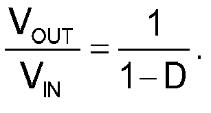
Fig. 10 : the mentioned point
- In comparison, the boost converter power stage with modulated-ramp PWM generator can be described by the static conversion ratio:

- For low control current values, this approximates a linear function of ICON as shown on
Fig. 11 : the maximum allowed control current ICON(MAX) which corresponds to the value where the PWM generator produces the duty-cycle value D MAX results from (8) as:
- Referring to
Fig. 11 , an illustration of the above equation (9), it is now referred to a power stage with the following parameters: Vin = 10V, L1 = 5µH, C1 = 22µF, RL = 150mΩ, RESR = 20mΩ, R = 100Ω Vb = 0.5V, C = 1pF, T = 0.3125µs (α = 1.6µA), RswU,D = 0. This power stage exhibits the point
Fig. 11 , this point is far from the considered dynamics of ICON , being between 1.6µA and 14µA (conversion ratio VOUT /VIN from 1 to 8). - Thus, and advantageously, the modulated-ramp PWM generator presents a natural duty cycle limitation by the maximal value of the control current IMAX and smooths the inflexion point, protecting the inductor current value. Regarding a safe choice of maximal control current value IMAX , (the maximal available control current ICON(MAX)), the averaged inductor current is revealed in the following expression (see
Fig. 11 ):
and the maximal inductor current is then limited to:
- Still referring to
Fig. 11 , the effect on the static conversion characteristic is shown, obtained by the averaged model of the power stage. One can observe, that for the conversion ratio up to 8, the inflexion point is far to occurs. - Referring now to
Figs. 16 and17 , practical benefits from the use of the modulated-ramp PWM generator are shows by measurement of a boost converter power stage. In these measurements, the PWM modulator uses the scheme fromFig. 7 with C = 71 pF (including parasitic capacitances), and clock frequency fsw = 500kHz. The power stage is built using an N-channel power MOSFET transistor with low RDSON < 100mΩ and a Schottky diode rectifier. The 0.5V bias voltage Vb results in α = VbC/T = 17.7x10⁻⁶ (6), which gives a control current range of 30 - 150µA (conversion ratio from 1 to 8). - The comparison of measured output voltage and output voltage calculated per the equation (5) is shown in
Fig. 16 . One can notice the low nonlinear conversion ratio error corresponding to the equation (8), which is caused by the low parasitic resistance of L (23mΩ). The small slope error is caused by the accuracy of capacitor C, and can be compensated by the Vb.
InFig. 17 , an example of a captured waveform of a converter operating with conversion ratio VOUT /VIN = 6.5 (e.g. with VIN = 5V and VOUT = 32V) is shown. Notably, one can observe the voltage ramp Vc , the bias voltage Vb , the switch voltage VLX and output voltage VOUT. Here, the dynamics of current source Ib is designed to provide high output impedance (high linearity) in the range 0 - Vb (i.e 0 - 500mV). Above, the low supply voltage causes the ramp to be nonlinear, what however, has no more impact to the conversion accuracy. - The ramp-modulated pulse width modulation generator described may be implemented on an integrated circuit, e.g. using transistors such as, but not limited to, CMOS transistors or MTCMOS transistors, and the like. Similarly, the switched-mode DC-to-DC converter may be implemented on an integrated circuit, e.g. using transistors such as, but not limited to, CMOS transistors or MTCMOS transistors, and the like. It is to be understood that the ramp-modulated pulse width modulation generator and/or the switched-mode DC-to-DC converter may be implemented with various electronic components suitable to perform the functions. The electronic components may be thus packaged discretely, as arrays or networks of like components, or integrated inside of packages such as semiconductor integrated circuits or thick film devices.
-
- [1] B. Bryant, M. K. Kazimierczuk, Voltage loop of boost PWM DC-DC converters with peak current-mode control IEEE Transactions on Circuits and Systems I: Vol. 53 , Issue: 1 2006
- [2] D. Liebal, P.Vijayraghavan, N.Sreenath, Control of DC-DC buck-boost converter using exact linearization techniques, IEEE Proc. of Power Electronics Specialists Conference PESC 1993.
- [3] H. Sira-Ramirez, M. Rios-Bolivar, A.S.I. Zinober, Adaptive input-output linearization for PWM regulation of DC-to-DC power converters Proc. of the American Control Conference, 1995.
- [4] Yu-Kang Lo, Shang-Chin Yen, Jan-Ming Wang, Linearization of the control-to-output transfer function for a PWM buck-boost converter Proc. IEEE International Symposium on Industrial Electronics, 2004 ,
- [5] D. Liebal, P.Vijayraghavan, N.Sreenath, Control of DC-DC buck-boost converter using exact linearization techniques, IEEE Proc. of Power Electronics Specialists Conference PESC 1993.
- [6] H. Sira-Ramirez, M. Rios-Bolivar, A.S.I. Zinober, Adaptive input-output linearization for PWM regulation of DC-to-DC power converters Proc. of the American Control Conference, 1995.
- [7] Yu-Kang Lo, Shang-Chin Yen, Jan-Ming Wang, Linearization of the control-to-output transfer function for a PWM buck-boost converter Proc. IEEE International Symposium on Industrial Electronics, 2004.
Claims (14)
- A ramp-modulated pulse width modulation generator (100) comprising:- an output stage (110) generating a ramp-modulated voltage (VD);- a control input (130) providing a variable multi-slope ramp voltage (VC);- a reference input (120) providing a constant voltage (Vb);- a comparator (140) connected to the control input and the reference input, the comparator comparing the voltage (VC) of the control input with the voltage (Vb) of the reference input to determine a duty-cycle ration of the ramp-modulated voltage (VD) generated as a result of the comparison.
- The ramp-modulated pulse width modulation generator of claim 1, wherein the control input is generated by a variable current (ICON) injected in a capacitor (C) periodically discharged.
- The ramp-modulated pulse width modulation generator of claim 2, wherein the variable current (ICON) is obtained from a control voltage (VCON) by a large value series resistance.
- The ramp-modulated pulse width modulation generator of claim 2, wherein the variable current (ICON) is obtained from a conversion of a control voltage (VCON) by using a CCII+ current conveyor circuit, the control voltage (VCON) being applied at the input node X of the CCII+ circuit, a resistance R such that R= VCON / ICON being connected to the input node Y, and the output Z of the of the CCII+ circuit providing the variable current (ICON).
- The ramp-modulated pulse width modulation generator of claim 2, wherein the variable current (ICON) is obtained from a non-inverting Howland current source.
- The ramp-modulated pulse width modulation generator of one of claims 1 to 5, wherein the variable multi-slope ramp voltage VC generated by the control input is one among:- saw-tooth wave ramp;- triangular wave ramp.
- A switched-mode DC to DC converter (200) converting an input voltage to an output voltage according to a signal control, wherein the switched-mode DC to DC converter comprises a ramp-modulated pulse width modulation generator (100) for generating the signal control, wherein the ramp-modulated pulse width modulation generator comprises:- an output stage (110) generating a ramp-modulated voltage (VD);- a control input (120) providing a variable multi-slope ramp voltage (VC);- a reference input (120) providing a constant voltage (Vb);- a comparator (140) connected to the control input and the reference input, the comparator comparing the voltage (VC) of the control input with the voltage (Vb) of the reference input to determine a duty-cycle ration of the ramp-modulated voltage (VD) generated as a result of the comparison.
- The switched-mode DC to DC converter of claim 7, wherein the control input is generated by a variable current (ICON) injected in a capacitor (C) periodically discharged.
- The switched-mode DC to DC converter of claim 7 or 8, wherein the switched-mode DC-to-DC converter is one among:- a Boost converter;- a Buck-Boost converter;- a Ćuk converter; and- a Sepic converter.
- The switched-mode DC-to-DC converter of one of claims 7 to 9, wherein the DC-to-DC converter is an open-loop DC-to-DC converter.
- The switched-mode DC-to-DC converter of one of claims 7 to 9, wherein the DC-to-DC converter is a closed-loop DC-to-DC converter.
- An integrated circuit comprising the ramp-modulated pulse width modulation generator according to one of claims 1 to 6.
- An integrated circuit comprising the switched-mode DC-to-DC converter according to one of claims 7 to 11.
- The integrated circuit of claim 12 or 13, wherein the integrated circuit is formed of one among:- CMOS transistors; and- MTCMOS transistors.
Priority Applications (2)
| Application Number | Priority Date | Filing Date | Title |
|---|---|---|---|
| EP11306557A EP2482433A3 (en) | 2011-01-27 | 2011-11-24 | Switched DC/DC boost power stage with linear control-to-output conversion ratio, based on a ramp-modulated PWM generator |
| PCT/EP2012/051273 WO2012101234A2 (en) | 2011-01-27 | 2012-01-26 | Switched dc/dc boost power stage with linear control-to-output conversion ratio, based on the ramp-modulated pwm generator |
Applications Claiming Priority (3)
| Application Number | Priority Date | Filing Date | Title |
|---|---|---|---|
| EP11368001 | 2011-01-27 | ||
| US201161471542P | 2011-04-04 | 2011-04-04 | |
| EP11306557A EP2482433A3 (en) | 2011-01-27 | 2011-11-24 | Switched DC/DC boost power stage with linear control-to-output conversion ratio, based on a ramp-modulated PWM generator |
Publications (2)
| Publication Number | Publication Date |
|---|---|
| EP2482433A2 true EP2482433A2 (en) | 2012-08-01 |
| EP2482433A3 EP2482433A3 (en) | 2012-11-21 |
Family
ID=45098992
Family Applications (1)
| Application Number | Title | Priority Date | Filing Date |
|---|---|---|---|
| EP11306557A Withdrawn EP2482433A3 (en) | 2011-01-27 | 2011-11-24 | Switched DC/DC boost power stage with linear control-to-output conversion ratio, based on a ramp-modulated PWM generator |
Country Status (2)
| Country | Link |
|---|---|
| EP (1) | EP2482433A3 (en) |
| WO (1) | WO2012101234A2 (en) |
Cited By (2)
| Publication number | Priority date | Publication date | Assignee | Title |
|---|---|---|---|---|
| US20150340952A1 (en) * | 2014-05-23 | 2015-11-26 | Texas Instruments Incorporated | Circuits and methods to linearize conversion gain in a dc-dc converter |
| CN115932639A (en) * | 2022-12-05 | 2023-04-07 | 七四九(南京)电子研究院有限公司 | Electronic load DC end control method and system |
Families Citing this family (2)
| Publication number | Priority date | Publication date | Assignee | Title |
|---|---|---|---|---|
| US11695356B2 (en) | 2020-10-06 | 2023-07-04 | Ford Global Technologies, Llc | Split gain transfer function for smart motor actuators |
| CN117869352A (en) * | 2024-02-05 | 2024-04-12 | 中国航发沈阳发动机研究所 | A method for controlling the angle of adjustable blades of an aircraft engine fan |
Family Cites Families (2)
| Publication number | Priority date | Publication date | Assignee | Title |
|---|---|---|---|---|
| US7126520B2 (en) * | 2004-01-30 | 2006-10-24 | Avago Technologies General Ip (Singapore) Pte. Ltd. | Segmented sawtooth generator |
| JP5642349B2 (en) * | 2009-02-05 | 2014-12-17 | フリースケール セミコンダクター インコーポレイテッド | Pulse width modulation circuit, pulse width modulation method and regulator |
-
2011
- 2011-11-24 EP EP11306557A patent/EP2482433A3/en not_active Withdrawn
-
2012
- 2012-01-26 WO PCT/EP2012/051273 patent/WO2012101234A2/en not_active Ceased
Non-Patent Citations (5)
| Title |
|---|
| B. BRYANT; M. K. KAZIMIERCZUK: "Voltage loop of boost PWM DC-DC converters with peak current-mode control IEEE Transactions", CIRCUITS AND SYSTEMS I, vol. 53, no. 1, 2006 |
| D. LIEBAL; P.VIJAYRAGHAVAN; N.SREENATH: "Control of DC-DC buck-boost converter using exact linearization techniques", IEEE PROC. OF POWER ELECTRONICS SPECIALISTS CONFERENCE PESC, 1993 |
| H. SIRA-RAMIREZ; M. RIOS-BOLIVAR; A.S.I. ZINOBER: "Adaptive input-output linearization for PWM regulation of DC-to-DC power converters", PROC. OF THE AMERICAN CONTROL CONFERENCE, 1995 |
| YU-KANG LO; SHANG-CHIN YEN; JAN-MING WANG: "Linearization of the control-to-output transfer function for a PWM buck-boost converter Proc", IEEE INTERNATIONAL SYMPOSIUM ON INDUSTRIAL ELECTRONICS, 2004 |
| YU-KANG LO; SHANG-CHIN YEN; JAN-MING WANG: "Linearization of the control-to-output transfer function for a PWM buck-boost converter", PROC. IEEE INTERNATIONAL SYMPOSIUM ON INDUSTRIAL ELECTRONICS, 2004 |
Cited By (4)
| Publication number | Priority date | Publication date | Assignee | Title |
|---|---|---|---|---|
| US20150340952A1 (en) * | 2014-05-23 | 2015-11-26 | Texas Instruments Incorporated | Circuits and methods to linearize conversion gain in a dc-dc converter |
| US9948181B2 (en) * | 2014-05-23 | 2018-04-17 | Texas Instruments Incorporated | Circuits and methods to linearize conversion gain in a DC-DC converter |
| US10594215B2 (en) | 2014-05-23 | 2020-03-17 | Texas Instruments Incorporated | Circuits and methods to linearize conversion gain in a DC-DC converter |
| CN115932639A (en) * | 2022-12-05 | 2023-04-07 | 七四九(南京)电子研究院有限公司 | Electronic load DC end control method and system |
Also Published As
| Publication number | Publication date |
|---|---|
| EP2482433A3 (en) | 2012-11-21 |
| WO2012101234A3 (en) | 2012-12-20 |
| WO2012101234A2 (en) | 2012-08-02 |
Similar Documents
| Publication | Publication Date | Title |
|---|---|---|
| CN114301268B (en) | Dynamic Biasing Technique for Current Sensing Based on On-Resistance of Enhancement-Mode MOSFET | |
| CN102931841B (en) | Multiphase DC-DC Power Converter | |
| US8129972B2 (en) | Single integrator sensorless current mode control for a switching power converter | |
| CN103401424B (en) | Systems and methods for adjusting output current of a power conversion system | |
| CN114094999B (en) | Converter circuit, corresponding device and method | |
| US10511226B1 (en) | Systems, methods, and apparatus for regulating a switched mode power supply | |
| US9948181B2 (en) | Circuits and methods to linearize conversion gain in a DC-DC converter | |
| KR20010033237A (en) | Discrete-time sampling of data for use in switching regulators | |
| JP4931530B2 (en) | Power converter | |
| CN1449594B (en) | Current Mode Switching Regulator | |
| US7498792B2 (en) | Pulse modulation system with nonlinear ramp | |
| US12341411B2 (en) | Methods and systems for current sensing | |
| EP3468022A1 (en) | Switch-mode power converter | |
| US10630183B2 (en) | Systems and methods for real-time inductor current simulation for a switching converter | |
| US20070018624A1 (en) | Current mode control with feed-forward for power devices | |
| WO2012101234A2 (en) | Switched dc/dc boost power stage with linear control-to-output conversion ratio, based on the ramp-modulated pwm generator | |
| US6552579B1 (en) | Fuel gauge power switch with current sense | |
| Trescases et al. | Sensorless digital peak current controller for low-power DC-DC SMPS based on a bi-directional delay line | |
| CN102629826A (en) | Switching regulator control circuit and switching regulator | |
| Michal | Modulated-ramp PWM generator for linear control of the boost converter's power stage | |
| EP4195482A1 (en) | Feedback circuit with adjustable loop gain for a boost converter | |
| CN103986333B (en) | system and method for adjusting output current of power supply conversion system | |
| US20230155471A1 (en) | Methods and Systems for Current Sensing in Power Converters | |
| WO2006127389A2 (en) | Power supply output monitor | |
| TWI627823B (en) | Power converting device |
Legal Events
| Date | Code | Title | Description |
|---|---|---|---|
| PUAI | Public reference made under article 153(3) epc to a published international application that has entered the european phase |
Free format text: ORIGINAL CODE: 0009012 |
|
| AK | Designated contracting states |
Kind code of ref document: A2 Designated state(s): AL AT BE BG CH CY CZ DE DK EE ES FI FR GB GR HR HU IE IS IT LI LT LU LV MC MK MT NL NO PL PT RO RS SE SI SK SM TR |
|
| AX | Request for extension of the european patent |
Extension state: BA ME |
|
| PUAL | Search report despatched |
Free format text: ORIGINAL CODE: 0009013 |
|
| AK | Designated contracting states |
Kind code of ref document: A3 Designated state(s): AL AT BE BG CH CY CZ DE DK EE ES FI FR GB GR HR HU IE IS IT LI LT LU LV MC MK MT NL NO PL PT RO RS SE SI SK SM TR |
|
| AX | Request for extension of the european patent |
Extension state: BA ME |
|
| RIC1 | Information provided on ipc code assigned before grant |
Ipc: H02M 3/156 20060101ALI20121017BHEP Ipc: H02M 1/08 20060101AFI20121017BHEP Ipc: H02M 3/155 20060101ALI20121017BHEP |
|
| STAA | Information on the status of an ep patent application or granted ep patent |
Free format text: STATUS: THE APPLICATION IS DEEMED TO BE WITHDRAWN |
|
| 18D | Application deemed to be withdrawn |
Effective date: 20130522 |