EP2479593A1 - Optical multiplexer/demultiplexer circuit - Google Patents
Optical multiplexer/demultiplexer circuit Download PDFInfo
- Publication number
- EP2479593A1 EP2479593A1 EP10816840A EP10816840A EP2479593A1 EP 2479593 A1 EP2479593 A1 EP 2479593A1 EP 10816840 A EP10816840 A EP 10816840A EP 10816840 A EP10816840 A EP 10816840A EP 2479593 A1 EP2479593 A1 EP 2479593A1
- Authority
- EP
- European Patent Office
- Prior art keywords
- optical
- demultiplexer
- waveguide
- waveguides
- arm
- Prior art date
- Legal status (The legal status is an assumption and is not a legal conclusion. Google has not performed a legal analysis and makes no representation as to the accuracy of the status listed.)
- Granted
Links
- 230000003287 optical effect Effects 0.000 title claims abstract description 517
- 230000005540 biological transmission Effects 0.000 claims abstract description 62
- 230000008878 coupling Effects 0.000 claims description 43
- 238000010168 coupling process Methods 0.000 claims description 43
- 238000005859 coupling reaction Methods 0.000 claims description 43
- 239000006185 dispersion Substances 0.000 claims description 35
- 238000004891 communication Methods 0.000 claims description 12
- 238000000411 transmission spectrum Methods 0.000 description 24
- 230000001360 synchronised effect Effects 0.000 description 16
- 238000009826 distribution Methods 0.000 description 15
- 230000005684 electric field Effects 0.000 description 6
- 230000015556 catabolic process Effects 0.000 description 5
- 238000006731 degradation reaction Methods 0.000 description 5
- 238000013461 design Methods 0.000 description 5
- 230000000694 effects Effects 0.000 description 5
- 230000002902 bimodal effect Effects 0.000 description 3
- 238000012545 processing Methods 0.000 description 3
- 238000004519 manufacturing process Methods 0.000 description 2
- NRNCYVBFPDDJNE-UHFFFAOYSA-N pemoline Chemical compound O1C(N)=NC(=O)C1C1=CC=CC=C1 NRNCYVBFPDDJNE-UHFFFAOYSA-N 0.000 description 2
- 229920006395 saturated elastomer Polymers 0.000 description 2
- VYPSYNLAJGMNEJ-UHFFFAOYSA-N Silicium dioxide Chemical compound O=[Si]=O VYPSYNLAJGMNEJ-UHFFFAOYSA-N 0.000 description 1
- XUIMIQQOPSSXEZ-UHFFFAOYSA-N Silicon Chemical compound [Si] XUIMIQQOPSSXEZ-UHFFFAOYSA-N 0.000 description 1
- 238000011161 development Methods 0.000 description 1
- 230000018109 developmental process Effects 0.000 description 1
- 238000005516 engineering process Methods 0.000 description 1
- 238000000034 method Methods 0.000 description 1
- 238000011160 research Methods 0.000 description 1
- 229910052710 silicon Inorganic materials 0.000 description 1
- 239000010703 silicon Substances 0.000 description 1
- 239000000758 substrate Substances 0.000 description 1
Images


Classifications
-
- G—PHYSICS
- G02—OPTICS
- G02B—OPTICAL ELEMENTS, SYSTEMS OR APPARATUS
- G02B6/00—Light guides; Structural details of arrangements comprising light guides and other optical elements, e.g. couplings
- G02B6/24—Coupling light guides
- G02B6/26—Optical coupling means
- G02B6/28—Optical coupling means having data bus means, i.e. plural waveguides interconnected and providing an inherently bidirectional system by mixing and splitting signals
- G02B6/293—Optical coupling means having data bus means, i.e. plural waveguides interconnected and providing an inherently bidirectional system by mixing and splitting signals with wavelength selective means
- G02B6/29379—Optical coupling means having data bus means, i.e. plural waveguides interconnected and providing an inherently bidirectional system by mixing and splitting signals with wavelength selective means characterised by the function or use of the complete device
- G02B6/29391—Power equalisation of different channels, e.g. power flattening
-
- G—PHYSICS
- G02—OPTICS
- G02B—OPTICAL ELEMENTS, SYSTEMS OR APPARATUS
- G02B6/00—Light guides; Structural details of arrangements comprising light guides and other optical elements, e.g. couplings
- G02B6/10—Light guides; Structural details of arrangements comprising light guides and other optical elements, e.g. couplings of the optical waveguide type
- G02B6/12—Light guides; Structural details of arrangements comprising light guides and other optical elements, e.g. couplings of the optical waveguide type of the integrated circuit kind
- G02B6/12007—Light guides; Structural details of arrangements comprising light guides and other optical elements, e.g. couplings of the optical waveguide type of the integrated circuit kind forming wavelength selective elements, e.g. multiplexer, demultiplexer
- G02B6/12009—Light guides; Structural details of arrangements comprising light guides and other optical elements, e.g. couplings of the optical waveguide type of the integrated circuit kind forming wavelength selective elements, e.g. multiplexer, demultiplexer comprising arrayed waveguide grating [AWG] devices, i.e. with a phased array of waveguides
- G02B6/12019—Light guides; Structural details of arrangements comprising light guides and other optical elements, e.g. couplings of the optical waveguide type of the integrated circuit kind forming wavelength selective elements, e.g. multiplexer, demultiplexer comprising arrayed waveguide grating [AWG] devices, i.e. with a phased array of waveguides characterised by the optical interconnection to or from the AWG devices, e.g. integration or coupling with lasers or photodiodes
- G02B6/12021—Comprising cascaded AWG devices; AWG multipass configuration; Plural AWG devices integrated on a single chip
-
- G—PHYSICS
- G02—OPTICS
- G02B—OPTICAL ELEMENTS, SYSTEMS OR APPARATUS
- G02B6/00—Light guides; Structural details of arrangements comprising light guides and other optical elements, e.g. couplings
- G02B6/10—Light guides; Structural details of arrangements comprising light guides and other optical elements, e.g. couplings of the optical waveguide type
- G02B6/12—Light guides; Structural details of arrangements comprising light guides and other optical elements, e.g. couplings of the optical waveguide type of the integrated circuit kind
- G02B6/12007—Light guides; Structural details of arrangements comprising light guides and other optical elements, e.g. couplings of the optical waveguide type of the integrated circuit kind forming wavelength selective elements, e.g. multiplexer, demultiplexer
- G02B6/12009—Light guides; Structural details of arrangements comprising light guides and other optical elements, e.g. couplings of the optical waveguide type of the integrated circuit kind forming wavelength selective elements, e.g. multiplexer, demultiplexer comprising arrayed waveguide grating [AWG] devices, i.e. with a phased array of waveguides
- G02B6/12019—Light guides; Structural details of arrangements comprising light guides and other optical elements, e.g. couplings of the optical waveguide type of the integrated circuit kind forming wavelength selective elements, e.g. multiplexer, demultiplexer comprising arrayed waveguide grating [AWG] devices, i.e. with a phased array of waveguides characterised by the optical interconnection to or from the AWG devices, e.g. integration or coupling with lasers or photodiodes
-
- G—PHYSICS
- G02—OPTICS
- G02B—OPTICAL ELEMENTS, SYSTEMS OR APPARATUS
- G02B6/00—Light guides; Structural details of arrangements comprising light guides and other optical elements, e.g. couplings
- G02B6/24—Coupling light guides
- G02B6/26—Optical coupling means
- G02B6/28—Optical coupling means having data bus means, i.e. plural waveguides interconnected and providing an inherently bidirectional system by mixing and splitting signals
- G02B6/293—Optical coupling means having data bus means, i.e. plural waveguides interconnected and providing an inherently bidirectional system by mixing and splitting signals with wavelength selective means
- G02B6/29379—Optical coupling means having data bus means, i.e. plural waveguides interconnected and providing an inherently bidirectional system by mixing and splitting signals with wavelength selective means characterised by the function or use of the complete device
- G02B6/2938—Optical coupling means having data bus means, i.e. plural waveguides interconnected and providing an inherently bidirectional system by mixing and splitting signals with wavelength selective means characterised by the function or use of the complete device for multiplexing or demultiplexing, i.e. combining or separating wavelengths, e.g. 1xN, NxM
-
- G—PHYSICS
- G02—OPTICS
- G02B—OPTICAL ELEMENTS, SYSTEMS OR APPARATUS
- G02B6/00—Light guides; Structural details of arrangements comprising light guides and other optical elements, e.g. couplings
- G02B6/10—Light guides; Structural details of arrangements comprising light guides and other optical elements, e.g. couplings of the optical waveguide type
- G02B6/12—Light guides; Structural details of arrangements comprising light guides and other optical elements, e.g. couplings of the optical waveguide type of the integrated circuit kind
- G02B2006/12133—Functions
- G02B2006/12159—Interferometer
-
- G—PHYSICS
- G02—OPTICS
- G02B—OPTICAL ELEMENTS, SYSTEMS OR APPARATUS
- G02B6/00—Light guides; Structural details of arrangements comprising light guides and other optical elements, e.g. couplings
- G02B6/10—Light guides; Structural details of arrangements comprising light guides and other optical elements, e.g. couplings of the optical waveguide type
- G02B6/12—Light guides; Structural details of arrangements comprising light guides and other optical elements, e.g. couplings of the optical waveguide type of the integrated circuit kind
- G02B6/12007—Light guides; Structural details of arrangements comprising light guides and other optical elements, e.g. couplings of the optical waveguide type of the integrated circuit kind forming wavelength selective elements, e.g. multiplexer, demultiplexer
- G02B6/12009—Light guides; Structural details of arrangements comprising light guides and other optical elements, e.g. couplings of the optical waveguide type of the integrated circuit kind forming wavelength selective elements, e.g. multiplexer, demultiplexer comprising arrayed waveguide grating [AWG] devices, i.e. with a phased array of waveguides
- G02B6/12016—Light guides; Structural details of arrangements comprising light guides and other optical elements, e.g. couplings of the optical waveguide type of the integrated circuit kind forming wavelength selective elements, e.g. multiplexer, demultiplexer comprising arrayed waveguide grating [AWG] devices, i.e. with a phased array of waveguides characterised by the input or output waveguides, e.g. tapered waveguide ends, coupled together pairs of output waveguides
-
- G—PHYSICS
- G02—OPTICS
- G02B—OPTICAL ELEMENTS, SYSTEMS OR APPARATUS
- G02B6/00—Light guides; Structural details of arrangements comprising light guides and other optical elements, e.g. couplings
- G02B6/24—Coupling light guides
- G02B6/26—Optical coupling means
- G02B6/28—Optical coupling means having data bus means, i.e. plural waveguides interconnected and providing an inherently bidirectional system by mixing and splitting signals
- G02B6/293—Optical coupling means having data bus means, i.e. plural waveguides interconnected and providing an inherently bidirectional system by mixing and splitting signals with wavelength selective means
- G02B6/29346—Optical coupling means having data bus means, i.e. plural waveguides interconnected and providing an inherently bidirectional system by mixing and splitting signals with wavelength selective means operating by wave or beam interference
- G02B6/2935—Mach-Zehnder configuration, i.e. comprising separate splitting and combining means
- G02B6/29352—Mach-Zehnder configuration, i.e. comprising separate splitting and combining means in a light guide
- G02B6/29355—Cascade arrangement of interferometers
Definitions
- the present invention relates to an optical wavelength multi/demultiplexer and, more specifically to an optical wavelength multi/demultiplexer including an arrayed waveguide grating.
- PLCs planar lightwave circuits
- AVGs Arrayed waveguide gratings
- AVGs optical wavelength multi/demultiplexers having a function of demultiplexing a multiplexed light signal having plural optical frequencies (a wavelength division multiplexed signal) into light signals with a predetermined optical frequency channel spacing or a function of multiplexing light signals ⁇ into a single wavelength division multiplexed signal.
- optical wavelength multi/demultiplexer used in such a system is required to have a broad and flat passband.
- optical wavelength multi/demultiplexers of flat transmission characteristics which have been proposed are a parabola AWG-type optical wavelength multi/demultiplexer including a parabola waveguide at an input end of a slab waveguide and an MZI-synchronized AWG optical wavelength multi/demultiplexer including a combination of a Mach-Zehnder Interferometer (MZI) and an AWG.
- FIG. 1 illustrates an example of the configuration of a parabola AWG type wavelength multi/demultiplexer.
- a parabola AWG-type wavelength multi/demultiplexer 100 includes a first slab waveguide 101, an arrayed-waveguide 102, a second slab waveguide 103, output waveguides 104, an input waveguide 105, and a parabola waveguide 106.
- Light incoming through the input waveguide 105 passes through the parabola waveguide 106 and then has a bimodal electric field distribution as shown in Fig. 2 .
- the light having the thus-obtained electric field distribution diffracts and passes through the first slab waveguide 101, and is then excited and propagates through each waveguide of the arrayed-waveguide 102.
- the light is focused at positions of the output waveguides 104 according to the optical frequencies in the second slab waveguide 103.
- the electric field distribution of the light focused at the interface between the slab waveguide 103 and the output waveguides 104 is also bimodal due to the reciprocity theorem.
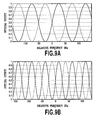
- the electric field distribution of the output waveguides 104 receiving the light is a Gaussian distribution as shown in Fig. 2 and has a small width. Accordingly, even if the optical frequency of the incoming light change to shift the light-focusing positions, the overlap integral of both the electric field distributions is kept constant, and thus flat transmission characteristics are obtained as shown in Fig. 3A .
- Fig. 3A shows a case of a channel spacing of 100 GHz (0.8 nm).
- Fig. 3B is an enlarged view of Fig. 3A .
- FIG. 4 illustrates an example of the configuration of an MZI-synchronized AWG type wavelength multi/demultiplexer.
- An MZI-synchronized AWG type wavelength multi/demultiplexer 400 includes a first slab waveguide 401, an arrayed-waveguide 402, a second slab waveguide 403, output waveguides 404, an input waveguide 405, a first optical coupler 406, a first arm waveguide 407, a second arm waveguide 408, and a second optical coupler 409.
- Light incoming through the input waveguide 405 is distributed to the first and second arm waveguides 407 and 408 by the second optical coupler 409, and thus the light beams have a phase difference according to the optical frequencies due to the optical path difference between the waveguides 407 and 408.
- the light beams traveling the arm waveguides are combined by the first optical coupler 406 to interfere with each other.
- the light focusing positions at the interface between the first optical coupler 406 and first slab waveguide 401 periodically changes according to the phase differences (or optical frequencies) between the light beams as shown in Figs. 5A and 5B .
- the light entering the first slab waveguide 401 from the first optical coupler 406 diffracts and is excited to propagate through each waveguide of the arrayed-waveguide 402.
- the light focusing positions in the second slab waveguide 403 vary according to the optical frequencies, and the light beams having desired optical frequencies are distributed to the respective output waveguides 404.
- the coordinate of the incident position of the optical field distribution output from the MZI circuit changes from a negative value to a positive value at the interface between the first optical coupler 406 and the first slab waveguide 401. If the change in optical frequency is neglected, the coordinate of the position at which the light beams are focused at the interface between the second slab waveguide 403 and output waveguide 404 changes from a positive value to a negative value due to the optical path differences in the arrayed-waveguide 402.
- the optical frequency changes from a lower frequency than the central frequency to a higher one
- the coordinate of the position at which the light beams are focused at the interface between the second slab waveguide 403 and the output waveguide 404 change from a negative value to a positive value due to the path length difference.
- the effects of both the cases are thus cancelled out with each other, and the light focusing position remains unchanged even if the optical frequency changes.
- the flat transmission characteristics shown in Figs. 6A and 6B can be obtained.
- the channel spacing in the drawings is 100 GHz (0.8 nm).
- NPL 1 B. Fondeur et al., "Ultrawide AWG with Hyper-Gaussian Profile", IEE Photonics Technology Letters, vol. 16, pp. 2628-2630, 2004
- transmission characteristics T(A) are approximated by a Hyper-Gaussian (HG) function as disclosed in NPL 1.
- BW 3dB is 3dB bandwidth; ⁇ c , central wavelength; and n, the degree of the HG function.
- Figs. 7A and 7B show the dependency of the light transmission characteristics on the degree of the HG function.
- n 2
- the transmission characteristics are expressed by a parabola function, and the larger the value of n, the more rectangular the light transmission characteristics.
- the present invention was made in the light of the above-described problem, and an object of the present invention is to provide an optical wavelength multi/demultiplexer having transmission characteristics with a higher rectangular degree than the conventional one.
- a first aspect of the invention is an optical wavelength multi/demultiplexer including: an AWG multi/demultiplexer and a two-stage lattice circuit connected to the AWG multi/demultiplexer, in which the AWG multi/demultiplexer includes: an arrayed waveguide grating; first and second slab waveguides connected to both ends of the arrayed waveguide grating; an input waveguide connected to the first slab waveguide; and an output waveguide connected to the second slab waveguide.
- the two-stage lattice circuit includes: a first optical coupler connected to another end of the first slab waveguide which is not connected to the arrayed-waveguide; first and second arm waveguides connected to the first optical coupler; a second optical coupler connected to other ends of the first and second arm waveguides which are not connected to the first optical coupler; third and fourth optical arm waveguides connected to the second optical coupler; a third optical coupler connected to other ends of the third and fourth arm waveguides which are not connected to the second optical coupler; and an input waveguide connected to the third optical coupler.
- an optical frequency period of the two-stage lattice circuit includes an optical frequency channel spacing of the arrayed waveguide grating and a period half the optical frequency channel spacing.
- a second aspect of the invention is characterized in the first aspect in that the first optical coupler has a coupling efficiency of 50%.
- a third aspect of the invention is characterized in the second aspect in that the second optical coupler has a coupling efficiency of 50%.
- a fourth aspect of the invention is characterized in the third aspect in that the third optical coupler has a coupling efficiency of not more than 20%.
- a fifth aspect of the invention is characterized in any one of the first to fourth aspects in that the optical frequency period defined by an optical path length difference between the first and second arm waveguides and an optical path length difference between the third and fourth arm waveguides is equal to the optical frequency channel spacing of the arrayed waveguide grating.
- a sixth aspect of the invention is characterized in any one of the first to fourth aspects in that: the optical frequency period defined by an optical path length difference between the first and second arm waveguides is equal to the optical frequency channel spacing of the arrayed waveguide grating; and the optical frequency period defined by an optical path length difference between the third and fourth arm waveguides is half the optical frequency period of the arrayed waveguide grating.
- a seventh aspect of the invention is an optical module including first optical multi/demultiplexer each being the optical wavelength multi/demultiplexer according to any one of the first to sixth aspects; and second optical multi/demultiplexer each being the optical wavelength multi/demultiplexer according to any one of first to sixth aspects.
- the second optical wavelength multi/demultiplexer having a same transmission waveform as that of the first optical multi/demultiplexer and having chromatic dispersion opposite to that of the first optical multi/demultiplexer by changing, to the opposite signs, both the plus or minus sign of a value of the optical path length difference between the first and second arm waveguides and the plus or minus sign of a value of the optical path length difference between the third and fourth arm waveguides; and by providing a cross waveguide between the first optical coupler and the first and second arm waveguides.
- the number of the first optical multi/demultiplexer is equal to the number of the second optical multi/demultiplexer in the same optical module.
- An eighth aspect of the invention an optical communication system including: first optical multi/demultiplexer each being the optical wavelength multi/demultiplexer according to any one of the first to sixth aspects; and second optical multi/demultiplexer each being the optical wavelength multi/demultiplexer according to any one of first to sixth aspects.
- the second optical wavelength multi/demultiplexer having a same transmission waveform as that of the first optical multi/demultiplexer and having chromatic dispersion opposite to that of the first optical multi/demultiplexer by changing, to the opposite signs, both the plus or minus sign of a value of the optical path length difference between the first and second arm waveguides and the plus or minus sign of a value of the optical path length difference between the third and fourth arm waveguides; and by providing a cross waveguide between the first optical coupler and the first and second arm waveguides.
- the number of the first optical multi/demultiplexer is equal to the number of the second optical multi/demultiplexer in a same transmission section.
- a ninth aspect of the invention is an optical module including first optical multi/demultiplexer each being the optical wavelength multi/demultiplexer according to any one of the first to sixth aspects; and second optical multi/demultiplexer each being the optical wavelength multi/demultiplexer according to any one of the first to sixth aspects.
- the second optical wavelength multi/demultiplexer having a same transmission waveform as that of the first optical multi/demultiplexer and having chromatic dispersion opposite to that of the first optical multi/demultiplexer by connecting the input waveguide to the other one of two input ports of the third optical coupler which are located at positions axisymmetric with respect to an axis of incidence, and by setting the phase difference between the first and second arm waveguides to 180 degrees to make the optical frequency channel spacing of the arrayed waveguide grating equal to the optical frequency period of the two-stage lattice circuit.
- the number of the first optical multi/demultiplexer is equal to the number of the second optical multi/demultiplexer in the same optical module.
- a tenth aspect of the invention is an optical communication system including: first optical multi/demultiplexer each being the optical wavelength multi/demultiplexer according to any one of the first to sixth aspects; and second optical multi/demultiplexer each being the optical wavelength multi/demultiplexer according to any one of the first to sixth aspects.
- the second optical wavelength multi/demultiplexer having a same transmission waveform as that of the first optical multi/demultiplexer and having chromatic dispersion opposite to that of the first optical multi/demultiplexer by connecting the input waveguide to the other one of two input ports of the third optical coupler which are located at positions axisymmetric with respect to an axis of incidence, and by setting the phase difference between the first and second arm waveguides to 180 degrees to make the optical frequency channel spacing of the arrayed waveguide grating equal to the optical frequency period of the two-stage lattice circuit.
- the number of the first optical multi/demultiplexer is equal to the number of the second optical multi/demultiplexer in a same transmission section.
- An eleventh aspect of the invention is characterized in the optical wavelength multi/demultiplexer according to any one of the first to sixth aspects in that each of a first delay circuit composed of the first and second arm waveguides and a second delay circuit composed of the third and fourth arm waveguides includes a folding portion in which the two-stage lattice circuit is arranged in a folded manner.
- the optical wavelength multi/demultiplexer including the arrayed waveguide grating and two-stage lattice circuit is designed so that the optical frequency period of the two-stage lattice circuit includes the optical frequency channel spacing of the arrayed waveguide grating and the period half the optical frequency channel spacing. This can increase the rectangular degree of the transmission characteristics compared to the conventional art and implement an optical multi/demultiplexer which is applicable to an advanced network in which optical signals pass through a number of points.
- an MZI-synchronized AWG-type optical wavelength multi/demultiplexer can be designed so that the effect of changes in light focusing position at the optical coupler end due to the phase differences in arm waveguides of the MZI is canceled with the effect of changes in light focusing position at the slab waveguide end due to the optical path length differences of arrayed-waveguides to keep the light focusing position in place in a wider optical frequency range, it is possible to provide flatter transmission characteristics with the rectangular degree improved.
- FIG. 8 shows a general MZI circuit.
- An MZI circuit 500 includes an input waveguide 501, a first optical coupler 502, a first arm waveguide 503, a second arm waveguide 504, a second optical coupler 505, and an output waveguide 506.
- the channel spacing is 100 GHz
- the optical path length difference ⁇ L between the first and the second arm waveguides 503 and 504 is 2023 ⁇ m.
- the optical path length difference ⁇ L between the first and second arm waveguides 503 and 504 produces a phase difference between light beams incoming through the input waveguide 501 according to the optical frequencies. Accordingly, as shown in Fig. 9A , the optical output changes with an optical frequency period of 100 GHz.
- the optical output changes with a half optical frequency period of 50 GHz as shown in Fig. 9B .
- the MZI circuit placed before the AWG includes an interference circuit provided with an optical path length difference including both components of ⁇ L and 2 ⁇ L
- the above-described changes in light focusing position at the optical coupler end can be controlled more precisely.
- the waveform can be reproduced more accurately by expansion using higher-order frequency components.
- the interference circuit in which the optical path length difference in the MZI circuit placed before the AWG includes components of not only ⁇ L but also 2 ⁇ L
- the changes in light focusing position at the optical coupler end can be controlled more accurately.
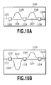
- a two-stage lattice circuit 1100 of Fig. 10A includes an input waveguide 1101, a third optical coupler 1102, a third arm waveguide 1103, a fourth arm waveguide 1104, a second optical coupler 1105, a first arm waveguide 1106, a second arm waveguide 1107, a first optical coupler 1108, and output waveguides 1109.
- the optical path length difference between the third and fourth arm waveguides 1103 and 1104 is designed to be ⁇ L
- the optical path length difference between the first and second arm waveguides 1106 and 1107 is designed to be ⁇ L.
- the path passing through the arm waveguides 1103 and 1106 has an optical path length difference of 2 ⁇ L from the path passing through the arm waveguides 1104 and 1107.
- Each path passing through the arm waveguides 1103 and 1107 and through the arm waveguides 1104 and 1106 has an optical path length difference of ⁇ L from the path passing through the arm waveguides 1104 and 1107.
- a two-stage lattice circuit 1110 of Fig. 10B includes an input waveguide 1111, a third optical coupler 1112, a third arm waveguide 1113, a fourth arm waveguide 1114, a second optical coupler 1115, a first arm waveguide 1116, a second arm waveguide 1117, a first optical coupler 1118, and output waveguides 1119.
- the optical path length difference between the third and fourth arm waveguides 1113 and 1114 is designed to be 2 ⁇ L
- the optical path length difference between the first and second arm waveguides 1116 and 1117 is designed to be ⁇ L.
- the path passing through the arm waveguides 1114 and 1117 has an optical path length difference of 2 ⁇ L from the path passing through the arm waveguides 1113 and 1117.
- the path passing through the arm waveguides 1113 and 1106 has an optical path length difference of ⁇ L from the path passing through the arm waveguides 1113 and 1117.
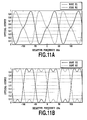
- Figs. 11A and 11B are charts showing optical outputs of the two-stage lattice circuits of Figs. 10A and 10B , respectively. Since the optical path differences include the components of not only ⁇ L but also 2 ⁇ L, the outputs thereof can be changed more steeply than the results of Fig. 9A . The rectangular degree of the transmission characteristics of the AWG can be therefore increased.
- the invention may include any splitter or coupler capable of achieving a predetermined coupling efficiency. It should be noted that an asymmetric Y branch, a multi-mode interference coupler (MMI), or the like may be applied, for example.
- MMI multi-mode interference coupler
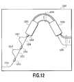
- FIG. 12 is a plan view illustrating an optical wavelength multi/demultiplexer according to a first embodiment of the invention.
- the first embodiment is a specific example including a two-stage lattice circuit of the type shown in Fig. 10A .
- a synchronized AWG-type optical multi/demultiplexer 1200 includes a first slab waveguide 1201, arrayed-waveguides 1202, a second slab waveguide 1203, output waveguides 1204, a first optical coupler 1206, a first arm waveguide 1207, a second arm waveguide 1208, and a second optical coupler 1209, a third arm waveguide 1210, a fourth arm waveguide 1211, a third optical coupler 1212, and an input waveguide 1205.
- the optical wavelength multi/demultiplexer 1200 has a relative refractive index difference ⁇ of 1.5% and a core thickness of 4.5 ⁇ m.
- the core widths of the input waveguide 1205, output waveguides 1204, arrayed-waveguides 1202, first arm waveguide 1207, second arm waveguide 1208, third arm waveguide 1210, and fourth arm waveguide 1211 are 4.5 ⁇ m.
- the portions of the arrayed-waveguides 1202 which are connected to the first and second slab waveguides 1201 and 1203 are positioned with a pitch of 10 ⁇ m.
- the number of the output waveguides 1204 are the same as the number of wavelength channels, and the portions of the output waveguides 1204 which are connected to the second slab waveguide 1203 are arranged with a pitch of 17 ⁇ m.
- a linear tapered waveguide is provided so as to have an opening width of 12.5 ⁇ m.
- the optical multi/demultiplexer 1200 is designed so that: the number of wavelength channels is 40; the optical frequency channel spacing, 100 GHz; the length of the first and second slab waveguides 1201 and 1203, 9566.85 ⁇ m; the number of arrayed-waveguides 1202, 187; and the optical path length difference between the arrayed-waveguides adjacent to each other, 33.98 ⁇ m.
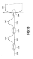
- Fig. 13 is an enlarged view of a part from the input waveguide 1205 to the first slab waveguide 1201 in Fig. 12 .
- the first to third optical couplers 1206, 1209, and 1212 include directional couplers.
- the waveguide width and waveguide pitch of the directional couplers are 4.5 ⁇ m and 6.5 ⁇ m, respectively.
- the coupling efficiencies of the first to third optical couplers 1206, 1209, and 1212 are designed to be 50%, 50%, and 8%, respectively.
- the optical path length differences between the first and second arm waveguides 1207 and 1208 and between the third and fourth arm waveguides 1210 and 1211 are both designed to be 2023 ⁇ m.
- the second optical coupler 1209 includes the directional coupler, but the invention is not limited to this configuration.
- Fig. 14 is an enlarged view around the second optical coupler in another configuration.
- the configuration of Fig. 14 employs a two-input two-output multi-mode interference coupler (MMI) 1400.
- the coupler 1400 has a width of 18 ⁇ m, a length of 740 ⁇ m, an input/output waveguide pitch of 12 ⁇ m, and a coupling efficiency of 50%.
- the coupling efficiency of the MMI is less affected by manufacturing errors than that of the directional couplers. Accordingly, the application of the MMI allows for implementation of an optical wavelength multi/demultiplexer having more excellent manufacturing tolerance.
- Figs. 16A and 16B are charts showing a transmission spectrum waveform of the optical wavelength multi/demultiplexer of this embodiment.
- Fig.17 shows a relationship between the coupling efficiency of the third optical coupler 1212 and the degree of the HG function of the transmission spectrum.
- Conventional example (1) shows the results of the parabola AWG-type
- Conventional example (2) shows the results of the synchronized MZI AWG-type.
- the degree of the HG function of this embodiment has a tendency to monotonically increase from a coupling efficiency of 6% and be saturated around a coupling efficiency of 20%.
- the results confirm that the rectangular degree of the transmission characteristics can be easily adjusted by changing the design of the coupling efficiency of the third optical coupler and a simple design can be provided.
- the third optical coupler since the rectangular degree is saturated around the coupling efficiency of 20% as described above, it is desirable that the third optical coupler have a coupling efficiency of 20% or less.
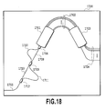
- FIG. 18 is a plan view illustrating an optical wavelength multi/demultiplexer according to a second embodiment of the invention.
- the second embodiment is a specific example including a two-stage lattice circuit of the type shown in Fig. 10B .
- a synchronized AWG-type optical multi/demultiplexer 1700 includes a first slab waveguide 1701, arrayed-waveguides 1702, a second slab waveguide 1703, output waveguides 1704, a first optical coupler 1706, a first arm waveguide 1707, a second arm waveguide 1708, a second optical coupler 1709, a third arm waveguide 1710, a fourth arm waveguide 1711, a third optical coupler 1712, and an input waveguide 1705.
- the optical wavelength multi/demultiplexer 1700 has a relative refractive index difference ⁇ of 1.5% and a core thickness of 4.5 ⁇ m.
- the core widths of the input waveguide 1705, output waveguides 1704, arrayed-waveguides 1702, first arm waveguide 1707, second arm waveguide 1708, third arm waveguide 1710, and fourth arm waveguide 1711 are 4.5 ⁇ m.
- the portions of the arrayed-waveguides 1702 which are connected to the first and second slab waveguides 1701 and 1703 are positioned with a pitch of 10 ⁇ m.
- the number of output waveguides 1704 is the same as the number of wavelength channels, and the portions of the output waveguides 1704 which are connected to the second slab waveguide 1703 are arranged with a pitch of 17 ⁇ m.
- a linear tapered waveguide is provided at the terminal end of each output waveguide 1704 so as to have an opening width of 12.5 ⁇ m.
- the optical multi/demultiplexer 1700 is designed so that: the number of wavelength channels is 40; the optical frequency channel spacing, 100 GHz; the length of the first and second slab waveguides 1701 and 1703, 9566.85 ⁇ m; the number of arrayed-waveguides 1702, 187; and the optical path length difference between the arrayed-waveguides adjacent to each other, 33.98 ⁇ m.
- Fig. 19 is an enlarged view of a part from the input waveguide 1705 to the first slab waveguide 1701.
- the first to third optical couplers 1706, 1709, and 1712 include directional couplers.
- the waveguide width and waveguide pitch of the directional couplers are 4.5 ⁇ m and 6.5 ⁇ m, respectively.
- the coupling efficiencies of the first to third optical couplers 1706, 1709, and 1712 are designed to be 50%, 50%, and 8%, respectively.
- the optical path length differences between the first and second arm waveguides 1707 and 1708 and between the third and fourth arm waveguides 1710 and 1711 are designed to be 2023 and 4046 ⁇ m, respectively.
- Figs. 21A and 21B are charts showing a transmission spectrum waveform of the optical wavelength multi/demultiplexer of this embodiment.
- this embodiment can achieve a 158% improvement in rectangular degree.
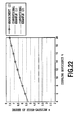
- Fig. 22 shows a relationship between the coupling efficiency of the third optical coupler 1712 and the degree of the HG function of the transmission spectrum.
- Conventional example (1) shows the results of the parabola AWG-type
- Conventional example (2) shows the results of the synchronized MZI AWG-type.
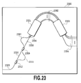
- FIG. 23 is a plan view illustrating an optical wavelength multi/demultiplexer according to a third embodiment of the invention.
- the third embodiment is a specific example including a two-stage lattice circuit of the type shown in Fig. 10B .
- a synchronized AWG-type optical multi/demultiplexer 2300 includes a first slab waveguide 2301, arrayed-waveguides 2302, a second slab waveguide 2303, output waveguides 2304, a first optical coupler 2306, a first arm waveguide 2307, a second arm waveguide 2308, a second optical coupler 2309, a third arm waveguide 2310, a fourth arm waveguide 2311, a third optical coupler 2312, and an input waveguide 2305.
- the optical wavelength multi/demultiplexer 2300 has a relative refractive index difference ⁇ of 1.5% and a core thickness of 4.5 ⁇ m.
- the core widths of the input waveguide 2305, output waveguides 2304, arrayed-waveguides 2302, first arm waveguide 2307, second arm waveguide 2308, third arm waveguide 2310, and fourth arm waveguide 2311 are 4.5 ⁇ m.
- the portions of the arrayed-waveguides 2302 which are connected to the first and second slab waveguides 2301 and 2303 are positioned with a pitch of 10 ⁇ m.
- the number of output waveguides 2304 is the same as the number of wavelength channels, and the portions of the output waveguides 2304 which are connected to the second slab waveguide 2303 are arranged with a pitch of 17 ⁇ m.
- a linear tapered waveguide is provided at the terminal end of each output waveguide 2304 so as to have an opening width of 12.5 ⁇ m.
- the optical multi/demultiplexer 2300 is designed so that: the number of wavelength channels is 40; the optical frequency channel spacing, 100 GHz; the lengths of the first and second slab waveguides 2301 and 2303, 9566.85 ⁇ m; the number of arrayed-waveguides 2302, 187; and the optical path length difference between the arrayed-waveguides adjacent to each other, 33.98 ⁇ m.
- Fig. 24 is an enlarged view of a part from the input waveguide 2305 to the first slab waveguide 2301.
- the first and second optical couplers 2306 and 2309 include directional couplers.
- the third optical coupler 2312 includes an asymmetric Y branch waveguide.
- the coupling efficiencies of the first and second optical couplers 2306 and 2309 are designed to be 50% and 62%, respectively.
- the asymmetric Y branch waveguide is designed to distribute optical power to the arm waveguides 2310 and 2311 at a branching ratio of 10% to 90%. If the optical power distributed to the arm waveguide 2310 is increased, the rectangular degree of the transmission waveform increases, but the excessive loss increases.
- the asymmetric Y branch waveguide is designed to distribute optical power to the arm waveguides 2310 and 2311 at a branching ratio of 10% to 90% so that the excessive loss is within 1 dB (see Figs. 25A and 25B ).
- the optical path length differences between the first and second arm waveguides 2307 and 2308 and between the third and fourth arm waveguides 2310 and 2311 are both designed to be 2023 ⁇ m.
- Figs. 26A and 26B are charts showing a transmission spectrum waveform of the optical wavelength multi/demultiplexer of this embodiment.
- this embodiment can achieve a 135% improvement of the rectangular degree.
- the first and second optical couplers are designed to have coupling efficiencies of 50%.
- the coupling efficiency of the second optical coupler is unnecessarily limited to 50%.
- the flat transmission characteristics can be changed to bimodal transmission characteristics including ripples to increase the rectangular degree.
- the allowable deviation of the coupling efficiency is thought to be about +/-10% around 50% (see Figs. 27A and 27B ).
- FIG. 28 is a plan view illustrating an optical wavelength multi/demultiplexer according to a fourth embodiment of the invention.
- the fourth embodiment is a specific example including a two-stage lattice circuit of the type shown in Fig. 10B .
- a synchronized AWG-type optical multi/demultiplexer 2600 includes a first slab waveguide 2601, arrayed-waveguides 2602, a second slab waveguide 2603, output waveguides 2604, a first optical coupler 2606, a first arm waveguide 2607, a second arm waveguide 2608, a second optical coupler 2609, a third arm waveguide 2610, a fourth arm waveguide 2611, a third optical coupler 2612, and an input waveguide 2605.
- the optical wavelength multi/demultiplexer 2600 has a relative refractive index difference ⁇ of 1.5% and a core thickness of 4.5 ⁇ m.
- the core widths of the input waveguide 2605, output waveguide 2604, arrayed-waveguides 2602, first arm waveguide 2607, second arm waveguide 2608, third arm waveguide 2610, and fourth arm waveguide 2611 are 4.5 ⁇ m.
- the portions of the array waveguides 2602 which are connected to the first and second slab waveguides 2601 and 2603 are positioned with a pitch of 10 ⁇ m.
- the number of output waveguides 2604 is the same as the number of wavelength channels, and the portions of the output waveguides 2604 which are connected to the second slab waveguide 2603 are arranged with a pitch or 17 ⁇ m.
- a linear tapered waveguide is provided at the terminal end of each output waveguide 2604 so as to have an opening width of 12.5 ⁇ m.
- the optical multi/demultiplexer 2600 is designed so that: the number of wavelength channels is 40; the optical frequency channel spacing, 100 GHz; the lengths of the first and second slab waveguides 2601 and 2603, 9566.85 ⁇ m; the number of arrayed-waveguides 2602, 187; and the optical path length difference between the arrayed-waveguides adjacent to each other, 33.98 ⁇ m.
- Fig. 29 is an enlarged view of a part from the input waveguide 2605 to the first slab waveguide 2601.
- the first and second optical couplers 2306 and 2609 include directional couplers.
- the third optical coupler 2612 includes an asymmetric Y branch waveguide.
- the coupling efficiencies of the first and second optical couplers 2606 and 2609 are designed to be 50% and 40%, respectively.
- the asymmetric Y branch waveguide 2612 is designed to distribute optical power to the third and fourth arm waveguides 2610 and 2611 at a branching ratio of 10% to 90%.
- the optical path length differences between the first and second arm waveguides 2607 and 2608 and between the third and fourth arm waveguides 2610 and 2611 are designed to be 2023 and 4046 ⁇ m, respectively.
- Figs. 30A and 30B are charts showing a transmission spectrum waveform of the optical wavelength multi/demultiplexer of this embodiment.
- this embodiment can achieve a 153% improvement in rectangular degree.
- the first and second optical couplers are designed to have coupling efficiencies of 50%.
- the coupling efficiency of the second optical coupler is unnecessarily limited to 50%. It is only necessary to implement a predetermined branching ratio, and the third coupler may include an asymmetric Y branch waveguide as shown in this embodiment.
- This embodiment is an optical multi/demultiplexer which has chromatic dispersion characteristics opposite to those of the first embodiment while keeping the broad transmission spectrum similar to the optical wavelength multi/demultiplexer of the first embodiment.
- the chromatic dispersion characteristics thereof can be canceled with each other, thus reducing the degradation in transmission quality due to the chromatic dispersion characteristics of the optical wavelength multi/demultiplexers.
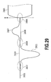
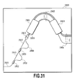
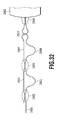
- Fig. 31 is a plan view illustrating a synchronized AWG-type optical wavelength multi/demultiplexer according to the fifth embodiment of the invention.
- the synchronized AWG-type optical multi/demultiplexer 2900 includes a first slab waveguide 2901, arrayed-waveguides 2902, a second slab waveguide 2903, output waveguides 2904, a first optical coupler 2906, a cross waveguide 2913, a first arm waveguide 2907, a second arm waveguide 2908, a second optical coupler 2909, a third arm waveguide 2910, a fourth arm waveguide 2911, a third optical coupler 2912, and an input waveguide 2905.
- the optical wavelength multi/demultiplexer 2900 has a relative refractive index difference ⁇ of 1.5% and a core thickness of 4.5 ⁇ m.
- the core widths of the input waveguide 2905, output waveguides 2904, arrayed-waveguides 2902, first arm waveguide 2907, second arm waveguide 2908, third arm waveguide 2910, and fourth arm waveguide 2911 are 4.5 ⁇ m.
- the portions of the arrayed-waveguides 2902 which are connected to the first and second slab waveguides 2901 and 2903 are positioned with a pitch of 10 ⁇ m.
- the number of output waveguides 2904 is the same as the number of wavelength channels, and the portions of the output waveguides which are connected to the second slab waveguide are arranged with a pitch of 17 ⁇ m.
- a linear tapered waveguide is provided at the terminal end of each output waveguide 2904 so as to have an opening width of 12.5 ⁇ m.
- the optical multi/demultiplexer 2900 is designed so that: the number of wavelength channels is 40; the optical frequency channel spacing, 100 GHz; the lengths of the first and second slab waveguides 2901 and 2903, 9566.85 ⁇ m; the number of arrayed-waveguides 2902, 187; and the optical path length difference between the arrayed-waveguides adjacent to each other, 33.98 ⁇ m.
- Fig. 32 is an enlarged view of a part from the input waveguide 2905 to the first slab waveguide 2901.
- the first to third optical couplers 2906, 2909, and 2912 include directional couplers.
- the waveguide width and pitch of the directional couplers are 4.5 ⁇ m and 6.5 ⁇ m, respectively.
- the coupling efficiencies of the first and second optical couplers 2906, 2909, and 2912 are designed to be 50%, 50%, and 8%, respectively.
- the optical path length differences between the first and second arm waveguides 2907 and 2908 and between the third and fourth arm waveguides 2910 and 2911 are designed to be 2023 ⁇ m, respectively.
- Figs. 33A and 33B are charts showing transmission spectra of the optical multi/demultiplexer of this embodiment and the optical wavelength multi/demultiplexer of the first embodiment.
- Fig. 33C is a chart showing chromatic dispersion characteristics of the optical multi/demultiplexer of this embodiment and the optical wavelength multi/demultiplexer of the first embodiment.
- the solid line shows the transmission characteristics of this embodiment, and the marks "o" show the transmission characteristics of the first embodiment.
- the charts can confirm that the fifth embodiment can provide a flat transmission spectrum similar to the first embodiment and the chromatic dispersion characteristics of the fifth and first embodiments are opposite to each other.
- the cross waveguide 2913 is used. Needless to say, using a directional coupler with a coupling efficiency of 100% instead can provide the equivalent effects.
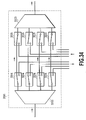
- Fig. 34 is a configuration view of an optical module fabricated using the optical wavelength multi/demultiplexers according to the fifth embodiment which have the opposite chromatic dispersion characteristics.
- the chromatic dispersion properties are canceled with each other.
- a plurality of optical devices are integrated into a single optical module.
- ROADM reconfigurable optical add drop module
- a WDM-multiplexed input signal is demultiplexed by an optical wavelength multi/demultiplexer for demultiplexing, and then the signals having different wavelengths are individually subjected to signal processing such as add/drop processing and are multiplexed again by the optical wavelength multi/demultiplexer to be output from the optical module.
- many optical modules integrally processing WDM signals include optical wavelength multi/demultiplexers for demultiplexing and optical wavelength multi/demultiplexers for multiplexing in pairs.
- the ROADM modules are used in a ring network and are required to avoid degradation of the quality of transmission signals even if optical signal travels through more than ten ROADM modules connected in series. Accordingly, individual ROADM modules are required to have a wider and flatter passband and lower chromatic dispersion.
- An optical module 3201 shown in Fig. 34 which is a ROADM module including the optical multi/demultiplexers of the invention, includes a first optical multi/demultiplexer 3202 for demultiplexing and a second optical multi/demultiplexer 3203 for multiplexing. Accordingly, the optical module 3201 has a wider and flatter passband than the conventional ROADM module, and moreover, the chromatic dispersion characteristics of the first multi/demultiplexer 3202 and the second optical multi/demultiplexer 3203 are canceled with each other to realize low chromatic dispersion characteristics as a whole of the optical module.
- Fig. 35 is a configuration view of an optical communication system according to the fifth embodiment.
- the optical communication system employs optical wavelength multi/demultiplexer having chromatic dispersion characteristics opposite to each other to reduce the degradation of transmission quality.
- each node 3305 is provided with only one optical wavelength multi/demultiplexer 3300.
- the nodes 3305 arranged on a ring network 3304 alternately use the first or second optical multi/demultiplexers 3302 or 3303, it is possible to implement a wider and flatter passband without accumulating chromatic dispersion at each section of a transmission path. Since the passband of each node is widened and the transmission amplitude characteristics and group delay characteristics are both flattened, it is possible to suppress degradation in transmission quality even if signals pass through a number of nodes.
- the opposite chromatic dispersion characteristics are obtained by changing, to the opposite sign, the plus or minus sign of the optical path length difference between the arm waveguides and using the cross waveguide.
- the opposite chromatic dispersion characteristics can be obtained with the transmission spectrum kept broad similar to the optical wavelength multi/demultiplexer according to the first embodiment in the following manner: an input port of the third optical coupler connected to the input waveguide is changed to the other one of the two input ports of the third optical coupler, and the phase difference between the first and second arm waveguides is adjusted so that the optical frequency channels of the arrayed waveguide grating correspond to those of the two-stage lattice circuit.
- the chromatic dispersion characteristics can be cancelled with each other, thus reducing the degradation in transmission quality due to the chromatic dispersion characteristics of the optical wavelength multi/demultiplexers.
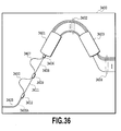
- FIG. 36 is a plan view illustrating the configuration of the synchronized AWG-type optical multi/demultiplexer of this embodiment.
- a synchronized AWG-type optical multi/demultiplexer 3400 includes a first slab waveguide 3401, arrayed-waveguides 3402, a second slab waveguide 3403, output waveguides 3404, a first optical coupler 3406, a first arm waveguide 3407, a second arm waveguide 3408, a second optical coupler 3409, a third arm waveguide 3410, a fourth arm waveguide 3411, a third optical coupler 3412, and an input waveguide 3405.
- the dashed line indicates an input waveguide 3405A included in the first embodiment.
- the optical wavelength multi/demultiplexer 3400 has a relative refractive index difference ⁇ of 1.5% and a core thickness of 4.5 ⁇ m.
- the core widths of the input waveguide 3405, output waveguides 3404, arrayed-waveguides 3402, first arm waveguide 3407, second arm waveguide 3408, third arm waveguide 3410, and fourth arm waveguide are 4.5 ⁇ m.
- the portions of the arrayed-waveguides 3402 which are connected to the first and second slab waveguides 3401 and 3403 are positioned with a pitch of 10 ⁇ m.
- the number of output waveguides 3404 is the same as the number of wavelength channels, and the portions of the output waveguides 3404 which are connected to the second slab waveguide are arranged with a pitch of 17 ⁇ m.
- a linear tapered waveguide is provided at the terminal end of each output waveguide 3404 so as to have an opening width of 12.5 ⁇ m.
- the optical multi/demultiplexer 3400 is designed so that: the number of wavelength channels is 40; the optical frequency channel spacing, 100 GHz; the lengths of the first and second slab waveguides 3401 and 2903, 9566.85 ⁇ m; the number of arrayed-waveguides 3402, 187; and the optical path length difference between the arrayed-waveguides adjacent to each other, 33.98 ⁇ m.
- Fig. 37 is an enlarged view of a part from the input waveguide 3405 to the first slab waveguide 3401.
- the first to third optical couplers 3406, 3409, and 3412 are composed of directional couplers.
- the waveguide width and pitch of the directional couplers are 4.5 ⁇ m and 6.5 ⁇ m, respectively.
- the coupling efficiencies of the first and second optical couplers 3406, 3409, and 3412 are designed to be 50%, 50%, and 8%, respectively.
- the optical path length differences between the first and second arm waveguides 3407 and 3408 and between the third and fourth arm waveguides 3410 and 3411 are designed to be 2023 ⁇ m.
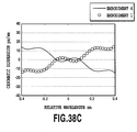
- Figs. 38A and 38B are charts showing transmission spectra of the optical multi/demultiplexer of this embodiment and the optical wavelength multi/demultiplexer of the second embodiment.
- Fig. 38C is a chart showing chromatic dispersion characteristics of the optical multi/demultiplexer of this embodiment and the optical wavelength multi/demultiplexer of the second embodiment.
- the solid line shows the transmission characteristics of this embodiment, and marks "o" show the transmission characteristics of the first embodiment.
- the charts confirm that the sixth embodiment can provide a flat transmission spectrum similar to the first embodiment and the chromatic dispersion characteristics of the sixth and first embodiments are opposite to each other.
- the third optical coupler 3412 includes two input ports 3405 and 3405A-located at upper and lower positions, respectively.
- the upper and lower positions of the two input ports 3405 and 3405A can be reversed.
- the input waveguide can be placed below the axis of incidence.
- optical wavelength multi/demultiplexer according to the seventh embodiment of the invention.
- two optical wavelength multi/demultiplexers having opposite chromatic dispersion characteristics are arranged with slab waveguides thereof crossing each other and are integrated in one chip.
- a first delay circuit including the first and second arm waveguides and a second delay circuit including the third and fourth arm waveguides each include folded portions to minimize the area occupied by the two-stage lattice circuit. This can increase the yields of chips per wafer.
- FIG. 39 is a plan view of a chip of this embodiment including two synchronized AWG-type optical multi/demultiplexers integrated.
- a first optical multi/demultiplexer 3700A includes a first slab waveguide 3701A, arrayed-waveguides 3702A, a second slab waveguide 3703A, output waveguides 3704A, a first optical coupler 3706A, a first arm waveguide 3707A, a second arm waveguide 3708A, a second optical coupler 3709A, a third arm waveguide 3710A, a fourth arm waveguide 3711A, a third optical coupler 3712A, and an input waveguide 3705A.
- a second optical multi/demultiplexer 3700B includes a first slab waveguide 3701B, arrayed-waveguides 3702B, a second slab waveguide 3703B, output waveguides 3704B, a first optical coupler 3706B, a first arm waveguide 3707B, a second arm waveguide 3708B, a second optical coupler 3709B, a third arm waveguide 3710B, a fourth arm waveguide 3711B, a third optical coupler 3712B, and an input waveguide 3705B.
- the first and second slab waveguides 3701A and 3703A of the first optical multi/demultiplexer 3700A intersect with the second and first slab waveguides 3703B and 3701B of the second optical multi/demultiplexer 3700B, respectively.
- the first and second optical wavelength multi/demultiplexers 3700A and 3700B have relative refractive index differences ⁇ of 1.5% and core thicknesses of 4.5 ⁇ m.
- the core widths of the input waveguides 3705A and 3705B, output waveguides 3704A and 3704B, arrayed-waveguides 3702A and 3702B, first arm waveguides 3707A and 3707B, second arm waveguides 3708A and 3708B, third arm waveguides 3710A and 3710B, and fourth arm waveguides 3711A and 3711B are 4.5 ⁇ m.
- the portions of the arrayed-waveguides 3702A which are connected to the first and second slab waveguides 3701A and 3703A are positioned with a pitch of 10 ⁇ m.
- the portions of the arrayed-waveguides 3702B which are connected to the first and second slab waveguides 3701B and 3703B are positioned with a pitch of 10 ⁇ m.
- the numbers of output waveguides 3704A and 3704B are the same as the number of wavelength channels.
- the portions of the output waveguides 3704A which are connected to the second slab waveguide are arranged with a pitch of 17 ⁇ m.
- the portions of the output waveguides 3704B which are connected to the second slab waveguide are arranged with a pitch of 17 ⁇ m.
- a linear tapered waveguide is provided so as to have an opening width of 12.5 ⁇ m.
- the optical multi/demultiplexer 3700 is designed so that: the numbers of wavelength channels are 40; the optical frequency channel spacings, 100 GHz; the lengths of the first slab waveguides 3701A and 3701B and the second slab waveguides 3703A and 3703B, 9566.85 ⁇ m; the numbers of arrayed-waveguides 3702A and 3702B, 187; and the optical path length difference between the arrayed-waveguides adjacent to each other, 33.98 ⁇ m.
- Fig. 40A is an enlarged view of a part of the first optical wavelength multi/demultiplexer 3700A from the input waveguide 3705A to the first slab waveguide 3701A.
- Fig. 40B is an enlarged view of a part of the second optical wavelength multi/demultiplexer 3700B from the input waveguide 3705B to the first slab waveguide 3701B.
- the first optical couplers 3706A and 3706B, second optical couplers 3709A and 3709B, and third optical couplers 3712A and 3712B include directional couplers.
- the waveguide width and pitch of the directional couplers are 4.5 ⁇ m and 6.5 ⁇ m, respectively.
- the coupling efficiencies of the first optical couplers 3706A and 3706B, second optical couplers 3709A and 3709B, and third optical couplers 3712A and 3712B are designed to be 50%, 50%, and 8%, respectively.
- the two-stage lattice circuit includes the couplers arranged on a straight line as shown in Fig. 13 . Accordingly, the distance that light incoming through the input waveguide 1205 travels to the first slab waveguide 1201 depends on the lengths of the arm waveguides 1210 and 1207, and the two-stage lattice circuit of the first embodiment occupies a large area. Accordingly, the yield of chips per wafer cannot be expected to increase.
- each two-stage lattice circuit is provided with the folded portions and thus is formed with a folded structure. This can reduce the occupied area and increase the yield of chips per wafer.
- the input waveguides 3705A and 3705B are respectively connected to the input ports of the third optical couplers 3712A and 3712B which are provided in the opposite sides to each other. Accordingly, as described in the sixth embodiment, the first and second wavelength multi/demultiplexers 3700A and 3700B have chromatic dispersion characteristics opposite to each other while keeping broad transmission spectra.
- the plus/minus sign of the optical path length difference between the first and second arm waveguides is equal to the plus/minus sign of the optical path length difference between the third and fourth arm waveguides.
- the plus/minus sign of the optical path length difference between the first and second arm waveguides is set different from the plus/minus sign of the optical path length difference between the third and fourth arm waveguides.
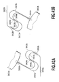
- Fig. 41 is a plan view of a chip of the eighth embodiment including two synchronized AWG-type optical multi/demultiplexers integrated.
- a first optical multi/demultiplexer 3900A includes a first slab waveguide 3901A, arrayed-waveguides 3902A, a second slab waveguide 3903A, output waveguides 3904A, a first optical coupler 3906A, a first arm waveguide 3907A, a second arm waveguide 3908A, a second optical coupler 3909A, a third arm waveguide 3910A, a fourth arm waveguide 3911A, a third optical coupler 3912A, and an input waveguide 3905A.
- a second optical multi/demultiplexer 3900B includes a first slab waveguide 3901B, arrayed-waveguides 3902B, a second slab waveguide 3903B, output waveguides 3904B, a first optical coupler 3906B, a first arm waveguide 3907B, a second arm waveguide 3908B, a second optical coupler 3909B, a third arm waveguide 3910B, a fourth arm waveguide 3911B, a third optical coupler 3912B, and an input waveguide 3905B.
- the first and second slab waveguides 3901A and 3903A of the first optical multi/demultiplexer 3900A intersect with the second and first slab waveguides 3903B and 3901B of the second optical multi/demultiplexer 3900B, respectively.
- the first and second optical wavelength multi/demultiplexers 3900A and 3900B have relative refractive index differences ⁇ of 1.5% and core thicknesses of 4.5 ⁇ m.
- the core widths of the input waveguides 3905A and 3905B, output waveguides 3904A and 3904B, arrayed-waveguides 3902A and 3902B, first arm waveguides 3907A and 3907B, second arm waveguides 3908A and 3908B, third arm waveguides 3910A and 3910B, and fourth arm waveguides 3911A and 3911B are 4.5 ⁇ m.
- the portions of the arrayed-waveguides 3902A which are connected to the first and second slab waveguides 3901A and 3903A are positioned with a pitch of 10 ⁇ m.
- the portions of the arrayed-waveguides 3902B which are connected to the first and second slab waveguides 3901B and 3903B are positioned with a pitch of 10 ⁇ m.
- the numbers of output waveguides 3904A and 3904B are the same as the number of wavelength channels.
- the portions of the output waveguides 3904A which are connected to the second slab waveguide are arranged with a pitch of 17 ⁇ m.
- the portions of the output waveguides 3904B which are connected to the second slab waveguide are arranged with a pitch of 17 ⁇ m.
- a linear tapered waveguide is provided so as to have an opening width of 12.5 ⁇ m.
- the optical multi/demultiplexers 3900A and 3900B are designed so that: the numbers of wavelength channels are 40; the optical frequency channel spacings, 100 GHz; the lengths of the first slab waveguides 3901A and 3901B and the second slab waveguides 3903A and 3903B, 9566.85 ⁇ m; the numbers of arrayed-waveguides 3902A and 3902B, 187; and the optical path length difference between the arrayed-waveguides adjacent to each other, 33.98 ⁇ m.
- Fig. 42A is an enlarged view of a part of the first optical wavelength multi/demultiplexer 3900A from the input waveguide 3905A to the first slab waveguide 3901A.
- Fig. 42B is an enlarged view of a part of the second optical wavelength multi/demultiplexer 3900B from the input waveguide 3905B to the first slab waveguide 3901B.
- the first optical couplers 3906A and 3906B, second optical couplers 3909A and 3909B, and third optical couplers 3912A and 3912B are composed of directional couplers.
- the waveguide width and pitch of the directional couplers are 4.5 ⁇ m and 6.5 ⁇ m, respectively.
- the coupling efficiencies of the first optical couplers 3906A and 3906B, second optical couplers 3009A and 3909B, and third optical couplers 3912A and 3912B are designed to be 50%, 150%, and 8%, respectively.
- Fig. 43 is a view for explaining the circuit configuration of Fig. 42 .
- 4101 indicates a first slab waveguide; 4105 and 4105A, input waveguides; 4106, a first optical coupler; 4107, a first arm waveguide; 4108, a second arm waveguide; 4109, a second optical coupler; 4110, a third arm waveguide; 4111, a fourth arm waveguide; 4112, a third optical coupler; and 4113, a cross waveguide.
- Use of the cross waveguide 4113 and input waveguide 4105A allows for implementation of the same configuration as that of the circuit of Fig. 13 .
- Use the cross waveguide 4113 and input waveguide 4105 allows for implementation of the same configuration as that of the circuit of Fig. 37 .
- the cross waveguide 4113 can be replaced with a coupler 4113A with a coupling efficiency of 100%. Accordingly, both of the optical coupler 4113A with a coupling efficiency of 100% and the optical coupler 4109 with a coupling efficiency of 50% are joined into one optical coupler 4109A.
- the optical coupler 4109A therefore needs to be designed to have a coupling efficiency of 150%.
- the input waveguides 3905A and 3905B of Fig. 42 are respectively connected to the input ports of the third optical couplers 3912A and 3912B which are provided in opposite sides to each other. Accordingly, as described in the sixth embodiment, the first and second optical wavelength multi/demultiplexers 3900A and 3900B can implement chromatic dispersion characteristics opposite to each other while keeping the broadband transmission spectrum.
Abstract
Description
- The present invention relates to an optical wavelength multi/demultiplexer and, more specifically to an optical wavelength multi/demultiplexer including an arrayed waveguide grating.
- Many researches and developments are actively made on planar lightwave circuits (PLCs) each including silica glass waveguides formed on a silicon substrate. Arrayed waveguide gratings (AWGs) using such PLC techniques play an important role in optical communication systems as optical wavelength multi/demultiplexers having a function of demultiplexing a multiplexed light signal having plural optical frequencies (a wavelength division multiplexed signal) into light signals with a predetermined optical frequency channel spacing or a function of multiplexing light signals·into a single wavelength division multiplexed signal.
- On the other hand, with the progress in optical communication systems, systems connecting plural points and flexibly switching communication paths, such as ring and mesh networks, are being constructed. In such an advanced network, light signals are required to pass through a number of points without being demodulated into electrical signals, and the optical wavelength multi/demultiplexer used in such a system is required to have a broad and flat passband. Such optical wavelength multi/demultiplexers of flat transmission characteristics which have been proposed are a parabola AWG-type optical wavelength multi/demultiplexer including a parabola waveguide at an input end of a slab waveguide and an MZI-synchronized AWG optical wavelength multi/demultiplexer including a combination of a Mach-Zehnder Interferometer (MZI) and an AWG. These related arts are disclosed in
PTLs -
Fig. 1 illustrates an example of the configuration of a parabola AWG type wavelength multi/demultiplexer. A parabola AWG-type wavelength multi/demultiplexer 100 includes afirst slab waveguide 101, an arrayed-waveguide 102, asecond slab waveguide 103,output waveguides 104, aninput waveguide 105, and aparabola waveguide 106. Light incoming through theinput waveguide 105 passes through theparabola waveguide 106 and then has a bimodal electric field distribution as shown inFig. 2 . The light having the thus-obtained electric field distribution diffracts and passes through thefirst slab waveguide 101, and is then excited and propagates through each waveguide of the arrayed-waveguide 102. The light is focused at positions of theoutput waveguides 104 according to the optical frequencies in thesecond slab waveguide 103. Herein, the electric field distribution of the light focused at the interface between theslab waveguide 103 and theoutput waveguides 104 is also bimodal due to the reciprocity theorem. On the other hand, the electric field distribution of theoutput waveguides 104 receiving the light is a Gaussian distribution as shown inFig. 2 and has a small width. Accordingly, even if the optical frequency of the incoming light change to shift the light-focusing positions, the overlap integral of both the electric field distributions is kept constant, and thus flat transmission characteristics are obtained as shown inFig. 3A . Herein,Fig. 3A shows a case of a channel spacing of 100 GHz (0.8 nm).Fig. 3B is an enlarged view ofFig. 3A . -
Fig. 4 illustrates an example of the configuration of an MZI-synchronized AWG type wavelength multi/demultiplexer. An MZI-synchronized AWG type wavelength multi/demultiplexer 400 includes afirst slab waveguide 401, an arrayed-waveguide 402, asecond slab waveguide 403,output waveguides 404, aninput waveguide 405, a firstoptical coupler 406, afirst arm waveguide 407, asecond arm waveguide 408, and a secondoptical coupler 409. Light incoming through theinput waveguide 405 is distributed to the first andsecond arm waveguides optical coupler 409, and thus the light beams have a phase difference according to the optical frequencies due to the optical path difference between thewaveguides optical coupler 406 to interfere with each other. The light focusing positions at the interface between the firstoptical coupler 406 andfirst slab waveguide 401 periodically changes according to the phase differences (or optical frequencies) between the light beams as shown inFigs. 5A and 5B . The light entering thefirst slab waveguide 401 from the firstoptical coupler 406 diffracts and is excited to propagate through each waveguide of the arrayed-waveguide 402. The light focusing positions in thesecond slab waveguide 403 vary according to the optical frequencies, and the light beams having desired optical frequencies are distributed to therespective output waveguides 404. - Next, a description is given of the principle to obtain the flat transmission characteristics. When the optical frequency changes from a lower frequency than the central frequency to a higher one, the coordinate of the incident position of the optical field distribution output from the MZI circuit changes from a negative value to a positive value at the interface between the first
optical coupler 406 and thefirst slab waveguide 401. If the change in optical frequency is neglected, the coordinate of the position at which the light beams are focused at the interface between thesecond slab waveguide 403 andoutput waveguide 404 changes from a positive value to a negative value due to the optical path differences in the arrayed-waveguide 402. Moreover, when the optical frequency changes from a lower frequency than the central frequency to a higher one, the coordinate of the position at which the light beams are focused at the interface between thesecond slab waveguide 403 and theoutput waveguide 404 change from a negative value to a positive value due to the path length difference. The effects of both the cases are thus cancelled out with each other, and the light focusing position remains unchanged even if the optical frequency changes. The flat transmission characteristics shown inFigs. 6A and 6B can be obtained. Herein, the channel spacing in the drawings is 100 GHz (0.8 nm). -
- PTL 1: Japanese Patent Laid-Open No.
9-297228 (1997 - PTL 2: Japanese Patent Laid-Open No.
8-69021 (1996 - NPL 1: B. Fondeur et al., "Ultrawide AWG with Hyper-Gaussian Profile", IEE Photonics Technology Letters, vol. 16, pp. 2628-2630, 2004
- In order to define the flatness of the aforementioned parabola AWG-type wavelength multi/demultiplexer and MZI-synchronized AWG-type light wavelength multi/demultiplexer, transmission characteristics T(A) are approximated by a Hyper-Gaussian (HG) function as disclosed in
NPL 1. -

- Herein, BW3dB is 3dB bandwidth; λc, central wavelength; and n, the degree of the HG function.
-
Figs. 7A and 7B show the dependency of the light transmission characteristics on the degree of the HG function. In the case of n=2, the transmission characteristics are expressed by a parabola function, and the larger the value of n, the more rectangular the light transmission characteristics. - If the transmission characteristics of the aforementioned parabola AWG type wavelength multi/demultiplexer are approximated by the HG function, the degree thereof is n=3.6 as shown in
Figs. 3A and 3B . On the other hand, if the transmission characteristics of the aforementioned MZI-synchronized AWG type wavelength multi/demultiplexer are approximated by the HG function, the degree thereof is n=4.0. According to the related art, it is difficult to implement transmission characteristics with a rectangular degree of n>4. - The present invention was made in the light of the above-described problem, and an object of the present invention is to provide an optical wavelength multi/demultiplexer having transmission characteristics with a higher rectangular degree than the conventional one.
- To achieve such an object, a first aspect of the invention is an optical wavelength multi/demultiplexer including: an AWG multi/demultiplexer and a two-stage lattice circuit connected to the AWG multi/demultiplexer, in which the AWG multi/demultiplexer includes: an arrayed waveguide grating; first and second slab waveguides connected to both ends of the arrayed waveguide grating; an input waveguide connected to the first slab waveguide; and an output waveguide connected to the second slab waveguide. The two-stage lattice circuit includes: a first optical coupler connected to another end of the first slab waveguide which is not connected to the arrayed-waveguide; first and second arm waveguides connected to the first optical coupler; a second optical coupler connected to other ends of the first and second arm waveguides which are not connected to the first optical coupler; third and fourth optical arm waveguides connected to the second optical coupler; a third optical coupler connected to other ends of the third and fourth arm waveguides which are not connected to the second optical coupler; and an input waveguide connected to the third optical coupler. In such an optical wavelength multi/demultiplexer, an optical frequency period of the two-stage lattice circuit includes an optical frequency channel spacing of the arrayed waveguide grating and a period half the optical frequency channel spacing.
- A second aspect of the invention is characterized in the first aspect in that the first optical coupler has a coupling efficiency of 50%.
- A third aspect of the invention is characterized in the second aspect in that the second optical coupler has a coupling efficiency of 50%.
- A fourth aspect of the invention is characterized in the third aspect in that the third optical coupler has a coupling efficiency of not more than 20%.
- A fifth aspect of the invention is characterized in any one of the first to fourth aspects in that the optical frequency period defined by an optical path length difference between the first and second arm waveguides and an optical path length difference between the third and fourth arm waveguides is equal to the optical frequency channel spacing of the arrayed waveguide grating.
- A sixth aspect of the invention is characterized in any one of the first to fourth aspects in that: the optical frequency period defined by an optical path length difference between the first and second arm waveguides is equal to the optical frequency channel spacing of the arrayed waveguide grating; and the optical frequency period defined by an optical path length difference between the third and fourth arm waveguides is half the optical frequency period of the arrayed waveguide grating.
- A seventh aspect of the invention is an optical module including first optical multi/demultiplexer each being the optical wavelength multi/demultiplexer according to any one of the first to sixth aspects; and second optical multi/demultiplexer each being the optical wavelength multi/demultiplexer according to any one of first to sixth aspects. The second optical wavelength multi/demultiplexer having a same transmission waveform as that of the first optical multi/demultiplexer and having chromatic dispersion opposite to that of the first optical multi/demultiplexer by changing, to the opposite signs, both the plus or minus sign of a value of the optical path length difference between the first and second arm waveguides and the plus or minus sign of a value of the optical path length difference between the third and fourth arm waveguides; and by providing a cross waveguide between the first optical coupler and the first and second arm waveguides. The number of the first optical multi/demultiplexer is equal to the number of the second optical multi/demultiplexer in the same optical module.
- An eighth aspect of the invention an optical communication system including: first optical multi/demultiplexer each being the optical wavelength multi/demultiplexer according to any one of the first to sixth aspects; and second optical multi/demultiplexer each being the optical wavelength multi/demultiplexer according to any one of first to sixth aspects. The second optical wavelength multi/demultiplexer having a same transmission waveform as that of the first optical multi/demultiplexer and having chromatic dispersion opposite to that of the first optical multi/demultiplexer by changing, to the opposite signs, both the plus or minus sign of a value of the optical path length difference between the first and second arm waveguides and the plus or minus sign of a value of the optical path length difference between the third and fourth arm waveguides; and by providing a cross waveguide between the first optical coupler and the first and second arm waveguides. The number of the first optical multi/demultiplexer is equal to the number of the second optical multi/demultiplexer in a same transmission section.
- A ninth aspect of the invention is an optical module including first optical multi/demultiplexer each being the optical wavelength multi/demultiplexer according to any one of the first to sixth aspects; and second optical multi/demultiplexer each being the optical wavelength multi/demultiplexer according to any one of the first to sixth aspects. The second optical wavelength multi/demultiplexer having a same transmission waveform as that of the first optical multi/demultiplexer and having chromatic dispersion opposite to that of the first optical multi/demultiplexer by connecting the input waveguide to the other one of two input ports of the third optical coupler which are located at positions axisymmetric with respect to an axis of incidence, and by setting the phase difference between the first and second arm waveguides to 180 degrees to make the optical frequency channel spacing of the arrayed waveguide grating equal to the optical frequency period of the two-stage lattice circuit. The number of the first optical multi/demultiplexer is equal to the number of the second optical multi/demultiplexer in the same optical module.
- A tenth aspect of the invention is an optical communication system including: first optical multi/demultiplexer each being the optical wavelength multi/demultiplexer according to any one of the first to sixth aspects; and second optical multi/demultiplexer each being the optical wavelength multi/demultiplexer according to any one of the first to sixth aspects. The second optical wavelength multi/demultiplexer having a same transmission waveform as that of the first optical multi/demultiplexer and having chromatic dispersion opposite to that of the first optical multi/demultiplexer by connecting the input waveguide to the other one of two input ports of the third optical coupler which are located at positions axisymmetric with respect to an axis of incidence, and by setting the phase difference between the first and second arm waveguides to 180 degrees to make the optical frequency channel spacing of the arrayed waveguide grating equal to the optical frequency period of the two-stage lattice circuit. The number of the first optical multi/demultiplexer is equal to the number of the second optical multi/demultiplexer in a same transmission section.
- An eleventh aspect of the invention is characterized in the optical wavelength multi/demultiplexer according to any one of the first to sixth aspects in that each of a first delay circuit composed of the first and second arm waveguides and a second delay circuit composed of the third and fourth arm waveguides includes a folding portion in which the two-stage lattice circuit is arranged in a folded manner.
- According to the present invention, the optical wavelength multi/demultiplexer including the arrayed waveguide grating and two-stage lattice circuit is designed so that the optical frequency period of the two-stage lattice circuit includes the optical frequency channel spacing of the arrayed waveguide grating and the period half the optical frequency channel spacing. This can increase the rectangular degree of the transmission characteristics compared to the conventional art and implement an optical multi/demultiplexer which is applicable to an advanced network in which optical signals pass through a number of points.
-
- [
Fig. 1] Fig. 1 is a configuration view of a conventional parabola AWG-type optical wavelength multi/demultiplexer; - [
Fig. 2] Fig. 2 is a view showing an electric field of aparabola waveguide 106 and anoutput waveguide 104 inFig. 1 ; - [
Fig. 3A] Fig. 3A is a chart showing the transmission characteristics of the parabola AWG-type optical wavelength multi/demultiplexer ofFig. 1 ; - [
Fig. 3B] Fig. 3B is a chart showing the transmission characteristics of the parabola AWG-type optical wavelength multi/demultiplexer ofFig. 1 ; - [
Fig. 4] Fig. 4 is a configuration view of a conventional MZI-synchronized AWG-type optical wavelength multi/demultiplexer; - [
Fig. 5A] Fig. 5A is a chart showing distributions of light focused at anoptical coupler 406 and afirst slab waveguide 401 inFig. 4 ; - [
Fig. 5B] Fig. 5B is a chart showing distributions of light focused at theoptical coupler 406 andfirst slab waveguide 401 inFig. 4 ; - [
Fig. 6A] Fig. 6A is a chart showing the transmission characteristics of the MZI-synchronized AWG-type optical wavelength multi/demultiplexer ofFig. 4 ; - [
Fig. 6B] Fig. 6B is a chart showing the transmission characteristics of the MZI-synchronized AWG-type optical wavelength multi/demultiplexer ofFig. 4 ; - [
Fig. 7A] Fig. 7A is a chart showing the dependency of the transmission characteristics on the degree of the HG function; - [
Fig. 7B] Fig. 7B is a chart showing the dependency of the transmission characteristics on the degree of the HG function. - [
Fig. 8] Fig. 8 is a view showing a general MZI circuit; - [
Fig. 9A] Fig. 9A is a chart showing an optical output of the MZI circuit ofFig. 8 ; - [
Fig. 9B] Fig. 9B is a chart showing the optical output of the MZI circuit ofFig. 8 ; - [
Fig. 10A] Fig. 10A is a configuration view of a two-stage lattice circuit according to the present invention; - [
Fig. 10B] Fig. 10B is a configuration view of the two-stage lattice circuit according to the present invention; - [
Fig. 11A] Fig. 11A is a chart showing the optical output of the two-stage lattice circuit ofFig. 10A ; - [
Fig. 11B] Fig. 11B is a chart showing the optical output of the two-stage lattice circuit ofFig. 10B ; - [
Fig. 12] Fig. 12 is a configuration view of an optical wavelength multi/demultiplexer according to a first embodiment of the present invention; - [
Fig. 13] Fig. 13 is an enlarged view of a part from aninput waveguide 1205 to afirst slab waveguide 1201 ofFig. 12 ; - [
Fig. 14] Fig. 14 is a view showing another configuration of a second optical coupler provided for the optical wavelength multi/demultiplexer according to the first embodiment; - [
Fig. 15A] Fig. 15A is a chart showing the distribution of light focused in a joint interface between a firstoptical coupler 1206 and thefirst slab waveguide 1201 ofFig. 13 ; - [
Fig. 15B] Fig. 15B is a chart showing the distribution of light focused in the joint interface between the firstoptical coupler 1206 andfirst slab waveguide 1201 ofFig. 13 ; - [
Fig. 16A] Fig. 16A is a chart showing the transmission characteristics of the optical wavelength multi/demultiplexer according to the first embodiment; - [
Fig. 16B] Fig. 16B is a chart showing the transmission characteristics of the optical wavelength multi/demultiplexer according to the first embodiment; - [
Fig. 17] Fig. 17 is a chart showing the relationship between the coupling efficiency of a thirdoptical coupler 1212 ofFig. 13 and the degree of the HG function of the transmission spectrum together with results of the conventional example; - [
Fig. 18] Fig. 18 is a configuration view of an optical wavelength multi/demultiplexer according to a second embodiment of the present invention; - [
Fig. 19] Fig. 19 is an enlarged view o a part from aninput waveguide 1705 to afirst slab waveguide 1701 ofFig. 18 ; - [
Fig. 20A] Fig. 20A is a chart showing a distribution of light focused in the joint interface between a firstoptical coupler 1706 and thefirst slab waveguide 1701 ofFig. 19 ; - [
Fig. 20B] Fig. 20B is a chart showing the distribution of light focused in the connecting interface between the firstoptical coupler 1706 and thefirst slab waveguide 1701 ofFig. 19 ; - [
Fig. 21A] Fig. 21A is a chart showing the transmission characteristics of the optical wavelength multi/demultiplexer according to the second embodiment; - [
Fig. 21B] Fig. 21B is a chart showing the transmission characteristics of the optical wavelength multi/demultiplexer according to the second embodiment; - [
Fig. 22] Fig. 22 is a chart showing the relationship between the coupling efficiency of a thirdoptical coupler 1712 ofFig. 18 and the degree of the HG function of the transmission spectrum together with the results of the conventional example; - [
Fig. 23] Fig. 23 is a configuration view of an optical wavelength multi/demultiplexer according to a third embodiment of a third embodiment; - [
Fig. 24] Fig. 24 is an enlarged view of a part from aninput waveguide 2305 to afirst slab waveguide 2301 ofFig. 23 ; - [
Fig. 25A] Fig. 25A is a chart showing the relationship between a power distribution ratio of a Y branching waveguide and the transmission characteristics; - [
Fig. 25B] Fig. 25B is a chart showing the relationship between the power distribution ratio of the Y branching waveguide and the transmission characteristics; - [
Fig. 26A] Fig. 26A is a chart showing the transmission characteristics of the optical wavelength multi/demultiplexer according to the third embodiment; - [
Fig. 26B] Fig. 26B is a chart showing the transmission characteristics of the optical wavelength multi/demultiplexer according to the third embodiment; - [
Fig. 27A] Fig. 27A is a chart showing the relationship between the deviation in coupling efficiency of a second optical coupler and the transmission characteristics; - [
Fig. 27B] Fig. 27B is a chart showing the relationship between the deviation of the coupling efficiency of the second optical coupler and the transmission characteristics; - [
Fig. 28] Fig. 28 is a configuration view of an optical wavelength multi/demultiplexer according to a fourth embodiment of the present invention; - [
Fig. 29] Fig. 29 is an enlarged view of a part from aninput waveguide 2605 to afirst slab waveguide 2601 ofFig. 26 ; [Fig. 30A] Fig. 30A is a chart showing the transmission characteristics of the optical wavelength multi/demultiplexer according to the fourth embodiment; - [
Fig. 30B] Fig. 30B is a chart showing the transmission characteristics of the optical wavelength multi/demultiplexer according to the fourth embodiment; - [
Fig. 31] Fig. 31 is a plan view illustrating the configuration of a synchronized AWG-type optical wavelength multi/demultiplexer according to a fifth embodiment; - [
Fig. 32] Fig. 32 is an enlarged view of a part from aninput waveguide 2905 to afirst slab waveguide 2901 ofFig. 28 ; - [
Fig. 33A] Fig. 33A is a chart showing transmission spectra of the optical multi/demultiplexers of the fifth and first embodiments; - [
Fig. 33B] Fig. 33B is a chart showing transmission spectra of the optical multi/demultiplexers of the fifth and first embodiments; - [
Fig. 33C] Fig. 33C is a chart showing chromatic dispersion characteristics of the optical multi/demultiplexers of the fifth and first embodiment; - [
Fig. 34] Fig. 34 is a configuration view of an optical module which is fabricated using optical wavelength multi/demultiplexers according to the fifth embodiment which have inverted chromatic dispersion characteristics to cancel the chromatic dispersion; - [
Fig. 35] Fig. 35 is a configuration view of an optical communication system according to the fifth embodiment; - [
Fig. 36] Fig. 36 is a plan view illustrating the configuration of a synchronized AWG-type optical wavelength multi/demultiplexer according to a sixth embodiment; - [
Fig. 37] Fig. 37 is an enlarged view of a part from aninput waveguide 3405 to afirst slab waveguide 3401 ofFig. 36 ; - [
Fig. 38A] Fig. 38A is a chart showing transmission spectra of the optical multi/demultiplexers of the sixth and second embodiments; - [
Fig. 38B] Fig. 38B is a chart showing transmission spectra of the optical multi/demultiplexers of the sixth and second embodiments; - [
Fig. 38C] Fig. 38C is a chart showing chromatic dispersion characteristics of the optical multi/demultiplexers of the sixth and second embodiment; - [
Fig. 39] Fig. 39 is a plan view of a chip of a seventh embodiment including two synchronized AWG-type optical wavelength multi/demultiplexers integrated; - [
Fig. 40A] Fig. 40A is an enlarged view of a part from aninput waveguide 3705A to afirst slab waveguide 3701A in a first optical wavelength multi/demultiplexer 3700A ofFig. 39 ; - [
Fig. 40B] Fig. 40B is an enlarged view of a part from an input waveguide 3700B to afirst slab waveguide 3701B in a second optical wavelength multi/demultiplexer 3700B ofFig. 39 ; - [
Fig. 41] Fig. 41 is a plan view of a chip of an eighth embodiment including two synchronized AWG-type optical wavelength multi/demultiplexers integrated; - [
Fig. 42A] Fig. 42A is an enlarged view of a part from aninput waveguide 3905A to afirst slab waveguide 3901A in a first optical wavelength multi/demultiplexer 3900A ofFig. 41 ; - [
Fig. 42B] Fig. 42B is an enlarged view of a part from aninput waveguide 3905B to afirst slab waveguide 3901B in a second optical wavelength multi/demultiplexer 3900B ofFig. 41 ; and - [
Fig. 43] Fig. 43 is a view for explaining the circuit configurations ofFigs. 42A and 42B . - Hereinafter, a description is given of embodiments of the present invention in detail with reference to the drawings.
- As described in the Background Art, if an MZI-synchronized AWG-type optical wavelength multi/demultiplexer can be designed so that the effect of changes in light focusing position at the optical coupler end due to the phase differences in arm waveguides of the MZI is canceled with the effect of changes in light focusing position at the slab waveguide end due to the optical path length differences of arrayed-waveguides to keep the light focusing position in place in a wider optical frequency range, it is possible to provide flatter transmission characteristics with the rectangular degree improved.
-
Fig. 8 shows a general MZI circuit. AnMZI circuit 500 includes aninput waveguide 501, a firstoptical coupler 502, afirst arm waveguide 503, asecond arm waveguide 504, a secondoptical coupler 505, and anoutput waveguide 506. - Herein, the channel spacing is 100 GHz, and the optical path length difference ΔL between the first and the
second arm waveguides second arm waveguides input waveguide 501 according to the optical frequencies. Accordingly, as shown inFig. 9A , the optical output changes with an optical frequency period of 100 GHz. Herein, if the optical path length difference is doubled, namely, set to 2·ΔL=4046 µm, the optical output changes with a half optical frequency period of 50 GHz as shown inFig. 9B . Accordingly, if the MZI circuit placed before the AWG includes an interference circuit provided with an optical path length difference including both components of ΔL and 2·ΔL, the above-described changes in light focusing position at the optical coupler end can be controlled more precisely. In Fourier series expansion of an arbitrary waveform, the waveform can be reproduced more accurately by expansion using higher-order frequency components. On the analogy of this fact, in the interference circuit in which the optical path length difference in the MZI circuit placed before the AWG includes components of not only ΔL but also 2·ΔL, the changes in light focusing position at the optical coupler end can be controlled more accurately. To be specific, it is necessary to apply the circuit configuration of a two-stage lattice circuit shown inFigs. 10A and 10B (the channel spacing is set to 100 GHz). - A two-
stage lattice circuit 1100 ofFig. 10A includes aninput waveguide 1101, a thirdoptical coupler 1102, a third arm waveguide 1103, afourth arm waveguide 1104, a secondoptical coupler 1105, a first arm waveguide 1106, asecond arm waveguide 1107, a firstoptical coupler 1108, andoutput waveguides 1109. The optical path length difference between the third andfourth arm waveguides 1103 and 1104 is designed to be ΔL, and the optical path length difference between the first andsecond arm waveguides 1106 and 1107 is designed to be ΔL. Accordingly, the path passing through the arm waveguides 1103 and 1106 has an optical path length difference of 2·ΔL from the path passing through thearm waveguides arm waveguides 1103 and 1107 and through thearm waveguides 1104 and 1106 has an optical path length difference of ΔL from the path passing through thearm waveguides - A two-
stage lattice circuit 1110 ofFig. 10B includes aninput waveguide 1111, a thirdoptical coupler 1112, athird arm waveguide 1113, afourth arm waveguide 1114, a secondoptical coupler 1115, afirst arm waveguide 1116, asecond arm waveguide 1117, a firstoptical coupler 1118, andoutput waveguides 1119. The optical path length difference between the third andfourth arm waveguides second arm waveguides arm waveguides arm waveguides arm waveguides 1113 and 1106 has an optical path length difference of ΔL from the path passing through thearm waveguides -
Figs. 11A and 11B are charts showing optical outputs of the two-stage lattice circuits ofFigs. 10A and 10B , respectively. Since the optical path differences include the components of not only ΔL but also 2·ΔL, the outputs thereof can be changed more steeply than the results ofFig. 9A . The rectangular degree of the transmission characteristics of the AWG can be therefore increased. - A description is given of some embodiments below. It should be noted that the present invention is not limited by particular numerals and the like shown in these embodiments. Moreover, the description is made mainly using directional couplers as a means of implementing optical couplers. However, the scope of the invention is not limited to this implementation means. The invention may include any splitter or coupler capable of achieving a predetermined coupling efficiency. It should be noted that an asymmetric Y branch, a multi-mode interference coupler (MMI), or the like may be applied, for example.
-
Fig. 12 is a plan view illustrating an optical wavelength multi/demultiplexer according to a first embodiment of the invention. The first embodiment is a specific example including a two-stage lattice circuit of the type shown inFig. 10A . A synchronized AWG-type optical multi/demultiplexer 1200 includes afirst slab waveguide 1201, arrayed-waveguides 1202, asecond slab waveguide 1203,output waveguides 1204, a firstoptical coupler 1206, afirst arm waveguide 1207, asecond arm waveguide 1208, and a secondoptical coupler 1209, athird arm waveguide 1210, afourth arm waveguide 1211, a thirdoptical coupler 1212, and aninput waveguide 1205. - The optical wavelength multi/
demultiplexer 1200 has a relative refractive index difference Δ of 1.5% and a core thickness of 4.5 µm. The core widths of theinput waveguide 1205,output waveguides 1204, arrayed-waveguides 1202,first arm waveguide 1207,second arm waveguide 1208,third arm waveguide 1210, andfourth arm waveguide 1211 are 4.5 µm. The portions of the arrayed-waveguides 1202 which are connected to the first andsecond slab waveguides output waveguides 1204 are the same as the number of wavelength channels, and the portions of theoutput waveguides 1204 which are connected to thesecond slab waveguide 1203 are arranged with a pitch of 17 µm. At the terminal end of eachoutput waveguide 1204, a linear tapered waveguide is provided so as to have an opening width of 12.5 µm. Moreover, the optical multi/demultiplexer 1200 is designed so that: the number of wavelength channels is 40; the optical frequency channel spacing, 100 GHz; the length of the first andsecond slab waveguides waveguides 1202, 187; and the optical path length difference between the arrayed-waveguides adjacent to each other, 33.98 µm. -
Fig. 13 is an enlarged view of a part from theinput waveguide 1205 to thefirst slab waveguide 1201 inFig. 12 . The first to thirdoptical couplers optical couplers second arm waveguides fourth arm waveguides - The second
optical coupler 1209 includes the directional coupler, but the invention is not limited to this configuration.Fig. 14 is an enlarged view around the second optical coupler in another configuration. The configuration ofFig. 14 employs a two-input two-output multi-mode interference coupler (MMI) 1400. Herein, thecoupler 1400 has a width of 18 μm, a length of 740 μm, an input/output waveguide pitch of 12 μm, and a coupling efficiency of 50%. The coupling efficiency of the MMI is less affected by manufacturing errors than that of the directional couplers. Accordingly, the application of the MMI allows for implementation of an optical wavelength multi/demultiplexer having more excellent manufacturing tolerance. - From
Figs. 15A and 15B , it can be confirmed that the light focusing position at the interface where the firstoptical coupler 1206 is joined to thefirst slab waveguide 1201 periodically changes according to the optical frequencies. -
Figs. 16A and 16B are charts showing a transmission spectrum waveform of the optical wavelength multi/demultiplexer of this embodiment. The charts reveal that the obtained transmission spectrum is flat. If the waveform is approximated by an HG function, the degree thereof is n=5.0. Compared with the MZI-synchronized AWG-type of the conventional art, whose degree of the HG function is n=4. 0, this embodiment can achieve a 125% improvement in rectangular degree. -
Fig.17 shows a relationship between the coupling efficiency of the thirdoptical coupler 1212 and the degree of the HG function of the transmission spectrum. Conventional example (1) shows the results of the parabola AWG-type, and Conventional example (2) shows the results of the synchronized MZI AWG-type. The degree of the HG function of this embodiment has a tendency to monotonically increase from a coupling efficiency of 6% and be saturated around a coupling efficiency of 20%. At this time, the rectangular degree achieves n=4.8 to 5.4. The results confirm that the rectangular degree of the transmission characteristics can be easily adjusted by changing the design of the coupling efficiency of the third optical coupler and a simple design can be provided. Moreover, since the rectangular degree is saturated around the coupling efficiency of 20% as described above, it is desirable that the third optical coupler have a coupling efficiency of 20% or less. -
Fig. 18 is a plan view illustrating an optical wavelength multi/demultiplexer according to a second embodiment of the invention. The second embodiment is a specific example including a two-stage lattice circuit of the type shown inFig. 10B . A synchronized AWG-type optical multi/demultiplexer 1700 includes afirst slab waveguide 1701, arrayed-waveguides 1702, asecond slab waveguide 1703,output waveguides 1704, a firstoptical coupler 1706, afirst arm waveguide 1707, asecond arm waveguide 1708, a secondoptical coupler 1709, athird arm waveguide 1710, afourth arm waveguide 1711, a thirdoptical coupler 1712, and aninput waveguide 1705. - The optical wavelength multi/
demultiplexer 1700 has a relative refractive index difference Δ of 1.5% and a core thickness of 4.5 µm. The core widths of theinput waveguide 1705,output waveguides 1704, arrayed-waveguides 1702,first arm waveguide 1707,second arm waveguide 1708,third arm waveguide 1710, andfourth arm waveguide 1711 are 4.5 μm. The portions of the arrayed-waveguides 1702 which are connected to the first andsecond slab waveguides output waveguides 1704 is the same as the number of wavelength channels, and the portions of theoutput waveguides 1704 which are connected to thesecond slab waveguide 1703 are arranged with a pitch of 17 μm. At the terminal end of eachoutput waveguide 1704, a linear tapered waveguide is provided so as to have an opening width of 12.5 μm. Moreover, the optical multi/demultiplexer 1700 is designed so that: the number of wavelength channels is 40; the optical frequency channel spacing, 100 GHz; the length of the first andsecond slab waveguides waveguides 1702, 187; and the optical path length difference between the arrayed-waveguides adjacent to each other, 33.98 μm. -
Fig. 19 is an enlarged view of a part from theinput waveguide 1705 to thefirst slab waveguide 1701. The first to thirdoptical couplers optical couplers second arm waveguides fourth arm waveguides - From
Figs. 20A and 20B , it can be confirmed that the light focusing position at the interface where the firstoptical coupler 1706 is joined to thefirst slab waveguide 1701 periodically changes according to the optical frequencies. -
Figs. 21A and 21B are charts showing a transmission spectrum waveform of the optical wavelength multi/demultiplexer of this embodiment. The charts reveal that the obtained transmission spectrum is flat. If the waveform is approximated by an HG function, the degree thereof is n=6.3. Compared with the MZI-synchronized AWG-type of the conventional art, whose degree of the HG function n is 4.0, this embodiment can achieve a 158% improvement in rectangular degree. -
Fig. 22 shows a relationship between the coupling efficiency of the thirdoptical coupler 1712 and the degree of the HG function of the transmission spectrum. Conventional example (1) shows the results of the parabola AWG-type, and Conventional example (2) shows the results of the synchronized MZI AWG-type. The degree of the HG function of this embodiment monotonically increases in a range of the coupling efficiency from 6% to 20%, and the rectangular degree reaches n=4. 9 to 7.6. Accordingly, by changing the design of the coupling efficiency of the thirdoptical coupler 1712, the rectangular degree of the transmission characteristics can be easily adjusted, and a simple design can be provided. -
Fig. 23 is a plan view illustrating an optical wavelength multi/demultiplexer according to a third embodiment of the invention. The third embodiment is a specific example including a two-stage lattice circuit of the type shown inFig. 10B . A synchronized AWG-type optical multi/demultiplexer 2300 includes afirst slab waveguide 2301, arrayed-waveguides 2302, asecond slab waveguide 2303,output waveguides 2304, a firstoptical coupler 2306, afirst arm waveguide 2307, asecond arm waveguide 2308, a secondoptical coupler 2309, athird arm waveguide 2310, afourth arm waveguide 2311, a thirdoptical coupler 2312, and aninput waveguide 2305. - The optical wavelength multi/
demultiplexer 2300 has a relative refractive index difference Δ of 1.5% and a core thickness of 4.5 μm. The core widths of theinput waveguide 2305,output waveguides 2304, arrayed-waveguides 2302,first arm waveguide 2307,second arm waveguide 2308,third arm waveguide 2310, andfourth arm waveguide 2311 are 4.5 μm. The portions of the arrayed-waveguides 2302 which are connected to the first andsecond slab waveguides output waveguides 2304 is the same as the number of wavelength channels, and the portions of theoutput waveguides 2304 which are connected to thesecond slab waveguide 2303 are arranged with a pitch of 17 μm. At the terminal end of eachoutput waveguide 2304, a linear tapered waveguide is provided so as to have an opening width of 12.5 μm. Moreover, the optical multi/demultiplexer 2300 is designed so that: the number of wavelength channels is 40; the optical frequency channel spacing, 100 GHz; the lengths of the first andsecond slab waveguides waveguides 2302, 187; and the optical path length difference between the arrayed-waveguides adjacent to each other, 33.98 μm. -
Fig. 24 is an enlarged view of a part from theinput waveguide 2305 to thefirst slab waveguide 2301. The first and secondoptical couplers optical coupler 2312 includes an asymmetric Y branch waveguide. The coupling efficiencies of the first and secondoptical couplers arm waveguides arm waveguide 2310 is increased, the rectangular degree of the transmission waveform increases, but the excessive loss increases. Herein, the asymmetric Y branch waveguide is designed to distribute optical power to thearm waveguides Figs. 25A and 25B ). The optical path length differences between the first andsecond arm waveguides fourth arm waveguides -
Figs. 26A and 26B are charts showing a transmission spectrum waveform of the optical wavelength multi/demultiplexer of this embodiment. The obtained transmission spectrum is flat, and if the waveform is approximated by an HG function, the degree thereof is n=5.4. Compared with the MZI-synchronized AWG-type of the conventional art, whose degree of the HG function n is 4.0, this embodiment can achieve a 135% improvement of the rectangular degree. To be specific, in the first and second embodiments, the first and second optical couplers are designed to have coupling efficiencies of 50%. However, as shown in this embodiment, the coupling efficiency of the second optical coupler is unnecessarily limited to 50%. By changing the coupling efficiency of the second optical coupler to a range from 40% to 60% instead of 50%, the flat transmission characteristics can be changed to bimodal transmission characteristics including ripples to increase the rectangular degree. On the other hand, if a large ripple exists in the passband of the optical multi/demultiplexer, the loss variation will degrade communication signals. Herein, the allowable deviation of the coupling efficiency is thought to be about +/-10% around 50% (seeFigs. 27A and 27B ). -
Fig. 28 is a plan view illustrating an optical wavelength multi/demultiplexer according to a fourth embodiment of the invention. The fourth embodiment is a specific example including a two-stage lattice circuit of the type shown inFig. 10B . A synchronized AWG-type optical multi/demultiplexer 2600 includes afirst slab waveguide 2601, arrayed-waveguides 2602, asecond slab waveguide 2603,output waveguides 2604, a firstoptical coupler 2606, afirst arm waveguide 2607, asecond arm waveguide 2608, a secondoptical coupler 2609, athird arm waveguide 2610, afourth arm waveguide 2611, a thirdoptical coupler 2612, and aninput waveguide 2605. - The optical wavelength multi/
demultiplexer 2600 has a relative refractive index difference Δ of 1.5% and a core thickness of 4.5 μm. The core widths of theinput waveguide 2605,output waveguide 2604, arrayed-waveguides 2602,first arm waveguide 2607,second arm waveguide 2608,third arm waveguide 2610, andfourth arm waveguide 2611 are 4.5 μm. The portions of thearray waveguides 2602 which are connected to the first andsecond slab waveguides output waveguides 2604 is the same as the number of wavelength channels, and the portions of theoutput waveguides 2604 which are connected to thesecond slab waveguide 2603 are arranged with a pitch or 17 μm. At the terminal end of eachoutput waveguide 2604, a linear tapered waveguide is provided so as to have an opening width of 12.5 μm. Moreover, the optical multi/demultiplexer 2600 is designed so that: the number of wavelength channels is 40; the optical frequency channel spacing, 100 GHz; the lengths of the first andsecond slab waveguides waveguides 2602, 187; and the optical path length difference between the arrayed-waveguides adjacent to each other, 33.98 μm. -
Fig. 29 is an enlarged view of a part from theinput waveguide 2605 to thefirst slab waveguide 2601. The first and secondoptical couplers optical coupler 2612 includes an asymmetric Y branch waveguide. The coupling efficiencies of the first and secondoptical couplers Y branch waveguide 2612 is designed to distribute optical power to the third andfourth arm waveguides second arm waveguides fourth arm waveguides -
Figs. 30A and 30B are charts showing a transmission spectrum waveform of the optical wavelength multi/demultiplexer of this embodiment. The obtained transmission spectrum is flat, and if the waveform is approximated by an HG function, the degree thereof is n=6.1. Compared with the MZI-synchronized AWG-type of the conventional art, whose degree of the HG function n is 4.0, this embodiment can achieve a 153% improvement in rectangular degree. To be specific, in the first and second embodiments, the first and second optical couplers are designed to have coupling efficiencies of 50%. However, as shown in this embodiment, the coupling efficiency of the second optical coupler is unnecessarily limited to 50%. It is only necessary to implement a predetermined branching ratio, and the third coupler may include an asymmetric Y branch waveguide as shown in this embodiment. - A description is given of an optical wavelength multi/demultiplexer according to a fifth embodiment of the invention. This embodiment is an optical multi/demultiplexer which has chromatic dispersion characteristics opposite to those of the first embodiment while keeping the broad transmission spectrum similar to the optical wavelength multi/demultiplexer of the first embodiment.
- In an optical module including equal numbers of optical wavelength multi/demultiplexers of the first embodiment and optical wavelength multi/demultiplexers of the fifth embodiment having opposite chromatic dispersion characteristics, the chromatic dispersion characteristics thereof can be canceled with each other, thus reducing the degradation in transmission quality due to the chromatic dispersion characteristics of the optical wavelength multi/demultiplexers.
-
Fig. 31 is a plan view illustrating a synchronized AWG-type optical wavelength multi/demultiplexer according to the fifth embodiment of the invention. The synchronized AWG-type optical multi/demultiplexer 2900 includes afirst slab waveguide 2901, arrayed-waveguides 2902, asecond slab waveguide 2903,output waveguides 2904, a firstoptical coupler 2906, across waveguide 2913, afirst arm waveguide 2907, asecond arm waveguide 2908, a secondoptical coupler 2909, athird arm waveguide 2910, afourth arm waveguide 2911, a thirdoptical coupler 2912, and aninput waveguide 2905. - The optical wavelength multi/
demultiplexer 2900 has a relative refractive index difference Δ of 1.5% and a core thickness of 4.5 μm. The core widths of theinput waveguide 2905,output waveguides 2904, arrayed-waveguides 2902,first arm waveguide 2907,second arm waveguide 2908,third arm waveguide 2910, andfourth arm waveguide 2911 are 4.5 μm. The portions of the arrayed-waveguides 2902 which are connected to the first andsecond slab waveguides output waveguides 2904 is the same as the number of wavelength channels, and the portions of the output waveguides which are connected to the second slab waveguide are arranged with a pitch of 17 μm. At the terminal end of eachoutput waveguide 2904, a linear tapered waveguide is provided so as to have an opening width of 12.5 μm. Moreover, the optical multi/demultiplexer 2900 is designed so that: the number of wavelength channels is 40; the optical frequency channel spacing, 100 GHz; the lengths of the first andsecond slab waveguides waveguides 2902, 187; and the optical path length difference between the arrayed-waveguides adjacent to each other, 33.98 μm. -
Fig. 32 is an enlarged view of a part from theinput waveguide 2905 to thefirst slab waveguide 2901. The first to thirdoptical couplers optical couplers second arm waveguides fourth arm waveguides -
Figs. 33A and33B are charts showing transmission spectra of the optical multi/demultiplexer of this embodiment and the optical wavelength multi/demultiplexer of the first embodiment.Fig. 33C is a chart showing chromatic dispersion characteristics of the optical multi/demultiplexer of this embodiment and the optical wavelength multi/demultiplexer of the first embodiment. The solid line shows the transmission characteristics of this embodiment, and the marks "o" show the transmission characteristics of the first embodiment. - The charts can confirm that the fifth embodiment can provide a flat transmission spectrum similar to the first embodiment and the chromatic dispersion characteristics of the fifth and first embodiments are opposite to each other.
- Furthermore, in the configuration view of the embodiment of
Fig. 31 , thecross waveguide 2913 is used. Needless to say, using a directional coupler with a coupling efficiency of 100% instead can provide the equivalent effects. -
Fig. 34 is a configuration view of an optical module fabricated using the optical wavelength multi/demultiplexers according to the fifth embodiment which have the opposite chromatic dispersion characteristics. In the optical module, the chromatic dispersion properties are canceled with each other. For the purposes of device miniaturization and cost reduction, a plurality of optical devices are integrated into a single optical module. One of the examples thereof is an optical module called ROADM (reconfigurable optical add drop module). In the ROADM module, a WDM-multiplexed input signal is demultiplexed by an optical wavelength multi/demultiplexer for demultiplexing, and then the signals having different wavelengths are individually subjected to signal processing such as add/drop processing and are multiplexed again by the optical wavelength multi/demultiplexer to be output from the optical module. In such a manner, many optical modules integrally processing WDM signals include optical wavelength multi/demultiplexers for demultiplexing and optical wavelength multi/demultiplexers for multiplexing in pairs. Moreover, the ROADM modules are used in a ring network and are required to avoid degradation of the quality of transmission signals even if optical signal travels through more than ten ROADM modules connected in series. Accordingly, individual ROADM modules are required to have a wider and flatter passband and lower chromatic dispersion. - An
optical module 3201 shown inFig. 34 , which is a ROADM module including the optical multi/demultiplexers of the invention, includes a first optical multi/demultiplexer 3202 for demultiplexing and a second optical multi/demultiplexer 3203 for multiplexing. Accordingly, theoptical module 3201 has a wider and flatter passband than the conventional ROADM module, and moreover, the chromatic dispersion characteristics of the first multi/demultiplexer 3202 and the second optical multi/demultiplexer 3203 are canceled with each other to realize low chromatic dispersion characteristics as a whole of the optical module. -
Fig. 35 is a configuration view of an optical communication system according to the fifth embodiment. The optical communication system employs optical wavelength multi/demultiplexer having chromatic dispersion characteristics opposite to each other to reduce the degradation of transmission quality. In anoptical communication system 3301 shown inFig. 35 , eachnode 3305 is provided with only one optical wavelength multi/demultiplexer 3300. However, if thenodes 3305 arranged on aring network 3304 alternately use the first or second optical multi/demultiplexers - A description is given of an optical wavelength multi/demultiplexer according to a sixth embodiment of the invention. In the fifth embodiment, the opposite chromatic dispersion characteristics are obtained by changing, to the opposite sign, the plus or minus sign of the optical path length difference between the arm waveguides and using the cross waveguide. In the sixth embodiment, the opposite chromatic dispersion characteristics can be obtained with the transmission spectrum kept broad similar to the optical wavelength multi/demultiplexer according to the first embodiment in the following manner: an input port of the third optical coupler connected to the input waveguide is changed to the other one of the two input ports of the third optical coupler, and the phase difference between the first and second arm waveguides is adjusted so that the optical frequency channels of the arrayed waveguide grating correspond to those of the two-stage lattice circuit..
- In an optical module including equal numbers of the optical wavelength multi/demultiplexers of the sixth embodiment having opposite chromatic dispersion characteristics and optical wavelength multi/demultiplexer of the first embodiment, the chromatic dispersion characteristics can be cancelled with each other, thus reducing the degradation in transmission quality due to the chromatic dispersion characteristics of the optical wavelength multi/demultiplexers.
-
Fig. 36 is a plan view illustrating the configuration of the synchronized AWG-type optical multi/demultiplexer of this embodiment. A synchronized AWG-type optical multi/demultiplexer 3400 includes afirst slab waveguide 3401, arrayed-waveguides 3402, asecond slab waveguide 3403,output waveguides 3404, a firstoptical coupler 3406, afirst arm waveguide 3407, asecond arm waveguide 3408, a secondoptical coupler 3409, athird arm waveguide 3410, afourth arm waveguide 3411, a thirdoptical coupler 3412, and aninput waveguide 3405. The dashed line indicates aninput waveguide 3405A included in the first embodiment. - The optical wavelength multi/
demultiplexer 3400 has a relative refractive index difference Δ of 1.5% and a core thickness of 4.5 μm. The core widths of theinput waveguide 3405,output waveguides 3404, arrayed-waveguides 3402,first arm waveguide 3407,second arm waveguide 3408,third arm waveguide 3410, and fourth arm waveguide are 4.5 μm. The portions of the arrayed-waveguides 3402 which are connected to the first andsecond slab waveguides output waveguides 3404 is the same as the number of wavelength channels, and the portions of theoutput waveguides 3404 which are connected to the second slab waveguide are arranged with a pitch of 17 μm. At the terminal end of eachoutput waveguide 3404, a linear tapered waveguide is provided so as to have an opening width of 12.5 μm. Moreover, the optical multi/demultiplexer 3400 is designed so that: the number of wavelength channels is 40; the optical frequency channel spacing, 100 GHz; the lengths of the first andsecond slab waveguides waveguides 3402, 187; and the optical path length difference between the arrayed-waveguides adjacent to each other, 33.98 μm. -
Fig. 37 is an enlarged view of a part from theinput waveguide 3405 to thefirst slab waveguide 3401. The first to thirdoptical couplers optical couplers second arm waveguides fourth arm waveguides -
Figs. 38A and38B are charts showing transmission spectra of the optical multi/demultiplexer of this embodiment and the optical wavelength multi/demultiplexer of the second embodiment.Fig. 38C is a chart showing chromatic dispersion characteristics of the optical multi/demultiplexer of this embodiment and the optical wavelength multi/demultiplexer of the second embodiment. The solid line shows the transmission characteristics of this embodiment, and marks "o" show the transmission characteristics of the first embodiment. - The charts confirm that the sixth embodiment can provide a flat transmission spectrum similar to the first embodiment and the chromatic dispersion characteristics of the sixth and first embodiments are opposite to each other.
- In the configuration view of the embodiment of
Fig. 37 , the thirdoptical coupler 3412 includes twoinput ports input waveguide 3405 andoptical coupler 3412, the upper and lower positions of the twoinput ports - Furthermore, in the configuration view of this embodiment of
Fig. 37 , if the coupling efficiency of theoptical coupler 3412 is set to 92% (=100-8)%, the input waveguide can be placed below the axis of incidence. - A description is given of an optical wavelength multi/demultiplexer according to the seventh embodiment of the invention. In the seventh embodiment, two optical wavelength multi/demultiplexers having opposite chromatic dispersion characteristics are arranged with slab waveguides thereof crossing each other and are integrated in one chip. Moreover, a first delay circuit including the first and second arm waveguides and a second delay circuit including the third and fourth arm waveguides each include folded portions to minimize the area occupied by the two-stage lattice circuit. This can increase the yields of chips per wafer.
-
Fig. 39 is a plan view of a chip of this embodiment including two synchronized AWG-type optical multi/demultiplexers integrated. A first optical multi/demultiplexer 3700A includes afirst slab waveguide 3701A, arrayed-waveguides 3702A, asecond slab waveguide 3703A,output waveguides 3704A, a firstoptical coupler 3706A, afirst arm waveguide 3707A, asecond arm waveguide 3708A, a secondoptical coupler 3709A, athird arm waveguide 3710A, afourth arm waveguide 3711A, a thirdoptical coupler 3712A, and aninput waveguide 3705A. A second optical multi/demultiplexer 3700B includes afirst slab waveguide 3701B, arrayed-waveguides 3702B, asecond slab waveguide 3703B,output waveguides 3704B, a firstoptical coupler 3706B, afirst arm waveguide 3707B, asecond arm waveguide 3708B, a secondoptical coupler 3709B, athird arm waveguide 3710B, afourth arm waveguide 3711B, a thirdoptical coupler 3712B, and aninput waveguide 3705B. The first andsecond slab waveguides first slab waveguides - The first and second optical wavelength multi/demultiplexers 3700A and 3700B have relative refractive index differences Δ of 1.5% and core thicknesses of 4.5 μm. The core widths of the
input waveguides output waveguides waveguides first arm waveguides second arm waveguides third arm waveguides fourth arm waveguides waveguides 3702A which are connected to the first andsecond slab waveguides waveguides 3702B which are connected to the first andsecond slab waveguides output waveguides output waveguides 3704A which are connected to the second slab waveguide are arranged with a pitch of 17 μm. The portions of theoutput waveguides 3704B which are connected to the second slab waveguide are arranged with a pitch of 17 μm. At the terminal end of each of theoutput waveguides demultiplexer 3700 is designed so that: the numbers of wavelength channels are 40; the optical frequency channel spacings, 100 GHz; the lengths of thefirst slab waveguides second slab waveguides waveguides -
Fig. 40A is an enlarged view of a part of the first optical wavelength multi/demultiplexer 3700A from theinput waveguide 3705A to thefirst slab waveguide 3701A.Fig. 40B is an enlarged view of a part of the second optical wavelength multi/demultiplexer 3700B from theinput waveguide 3705B to thefirst slab waveguide 3701B. The firstoptical couplers optical couplers optical couplers optical couplers optical couplers optical couplers - In the first embodiment, the two-stage lattice circuit includes the couplers arranged on a straight line as shown in
Fig. 13 . Accordingly, the distance that light incoming through theinput waveguide 1205 travels to thefirst slab waveguide 1201 depends on the lengths of thearm waveguides Fig. 40A of this embodiment, each two-stage lattice circuit is provided with the folded portions and thus is formed with a folded structure. This can reduce the occupied area and increase the yield of chips per wafer. - Moreover, the
input waveguides optical couplers - A description is given of an optical wavelength multi/demultiplexer according to an eighth embodiment of the invention. In the fifth embodiment, the plus/minus sign of the optical path length difference between the first and second arm waveguides is equal to the plus/minus sign of the optical path length difference between the third and fourth arm waveguides. In this configuration, the plus/minus sign of the optical path length difference between the first and second arm waveguides is set different from the plus/minus sign of the optical path length difference between the third and fourth arm waveguides. Such a configuration allows for a design facilitating the arrangement of the delay circuits having folded shapes.
-
Fig. 41 is a plan view of a chip of the eighth embodiment including two synchronized AWG-type optical multi/demultiplexers integrated. A first optical multi/demultiplexer 3900A includes afirst slab waveguide 3901A, arrayed-waveguides 3902A, asecond slab waveguide 3903A,output waveguides 3904A, a firstoptical coupler 3906A, afirst arm waveguide 3907A, asecond arm waveguide 3908A, a secondoptical coupler 3909A, athird arm waveguide 3910A, afourth arm waveguide 3911A, a thirdoptical coupler 3912A, and aninput waveguide 3905A. A second optical multi/demultiplexer 3900B includes afirst slab waveguide 3901B, arrayed-waveguides 3902B, asecond slab waveguide 3903B,output waveguides 3904B, a firstoptical coupler 3906B, afirst arm waveguide 3907B, asecond arm waveguide 3908B, a secondoptical coupler 3909B, athird arm waveguide 3910B, afourth arm waveguide 3911B, a thirdoptical coupler 3912B, and aninput waveguide 3905B. The first andsecond slab waveguides first slab waveguides - The first and second optical wavelength multi/demultiplexers 3900A and 3900B have relative refractive index differences Δ of 1.5% and core thicknesses of 4.5 μm. The core widths of the
input waveguides output waveguides waveguides first arm waveguides second arm waveguides third arm waveguides fourth arm waveguides waveguides 3902A which are connected to the first andsecond slab waveguides waveguides 3902B which are connected to the first andsecond slab waveguides output waveguides output waveguides 3904A which are connected to the second slab waveguide are arranged with a pitch of 17 μm. The portions of theoutput waveguides 3904B which are connected to the second slab waveguide are arranged with a pitch of 17 μm. At the terminal end of each of theoutput waveguides first slab waveguides second slab waveguides waveguides -
Fig. 42A is an enlarged view of a part of the first optical wavelength multi/demultiplexer 3900A from theinput waveguide 3905A to thefirst slab waveguide 3901A.Fig. 42B is an enlarged view of a part of the second optical wavelength multi/demultiplexer 3900B from theinput waveguide 3905B to thefirst slab waveguide 3901B. The firstoptical couplers optical couplers optical couplers optical couplers optical couplers 3009A and 3909B, and thirdoptical couplers -
Fig. 43 is a view for explaining the circuit configuration ofFig. 42 . Herein, 4101 indicates a first slab waveguide; 4105 and 4105A, input waveguides; 4106, a first optical coupler; 4107, a first arm waveguide; 4108, a second arm waveguide; 4109, a second optical coupler; 4110, a third arm waveguide; 4111, a fourth arm waveguide; 4112, a third optical coupler; and 4113, a cross waveguide. Use of thecross waveguide 4113 andinput waveguide 4105A allows for implementation of the same configuration as that of the circuit ofFig. 13 . Use thecross waveguide 4113 andinput waveguide 4105 allows for implementation of the same configuration as that of the circuit ofFig. 37 . - Actually, the
cross waveguide 4113 can be replaced with acoupler 4113A with a coupling efficiency of 100%. Accordingly, both of theoptical coupler 4113A with a coupling efficiency of 100% and theoptical coupler 4109 with a coupling efficiency of 50% are joined into oneoptical coupler 4109A. Theoptical coupler 4109A therefore needs to be designed to have a coupling efficiency of 150%. - On the other hand, the
input waveguides Fig. 42 are respectively connected to the input ports of the thirdoptical couplers
Claims (11)
- An optical wavelength multi/demultiplexer, comprising:an arrayed waveguide grating, anda two-stage lattice circuit connected to the arrayed waveguide grating, whereinthe arrayed waveguide grating includes: an arrayed waveguide; first and second slab waveguides connected to both ends of the arrayed-waveguide; and an output waveguide connected to the second slab waveguide, andthe two-stage lattice circuit includes: a first optical coupler connected to another end of the first slab waveguide which is not connected to the arrayed-waveguide; first and second arm waveguides connected to the first optical coupler; a second optical coupler connected to other ends of the first and second arm waveguides which are not connected to the first optical coupler; third and fourth arm waveguides connected to the second optical coupler; a third optical coupler connected to other ends of the third and fourth arm waveguides which are not connected to the second optical coupler; and an input waveguide connected to the third optical coupler, andan optical frequency period of the two-stage lattice circuit includes an optical frequency channel spacing of the arrayed waveguide grating and a period two times the optical frequency channel spacing.
- The optical wavelength multi/demultiplexer according to claim 1, wherein the first optical coupler has a coupling efficiency of 50%.
- The optical wavelength multi/demultiplexer according to claim 2, wherein the second optical coupler has a coupling efficiency of 50%.
- The optical wavelength multi/demultiplexer according to claim 3, wherein the third optical coupler has a coupling efficiency of not more than 20%.
- The optical wavelength multi/demultiplexer according to any one of claims 1 to 4, wherein the optical frequency period defined by an optical path length difference between the first and second arm waveguides and an optical path length difference between the third and fourth arm waveguides is equal to the optical frequency channel spacing of the arrayed waveguide grating .
- The optical wavelength multi/demultiplexer according to any one of claims 1 to 4, wherein the optical frequency period defined by an optical path length difference between the first and second arm waveguides is equal to the optical frequency channel spacing of the arrayed waveguide grating, and
the optical frequency period defined by an optical path length difference between the third and fourth arm waveguides is half the optical frequency period of the arrayed waveguide grating. - An optical module, comprising:first optical multi/demultiplexer each being the optical wavelength multi/demultiplexer according to any one of claims 1 to 6; andsecond optical multi/demultiplexer each being the optical wavelength multi/demultiplexer according to any one of claims 1 to 6, the second optical wavelength multi/demultiplexer having a same transmission waveform as that of the first optical multi/demultiplexer and having chromatic dispersion opposite to that of the first optical multi/demultiplexer by changing, to the opposite signs, both the plus or minus sign of a value of the optical path length difference between the first and second arm waveguides and the plus or minus sign of a value of the optical path length difference between the third and fourth arm waveguides; and by providing a cross waveguide between the first optical coupler and the first and second arm waveguides, whereinthe number of the first optical multi/demultiplexer is equal to the number of the second optical multi/demultiplexer in the same optical module.
- An optical communication system, comprising:first optical multi/demultiplexer each being the optical wavelength multi/demultiplexer according to any one of claims 1 to 6; andsecond optical multi/demultiplexer each being the optical wavelength multi/demultiplexer according to any one of claims 1 to 6, the second optical wavelength multi/demultiplexer having a same transmission waveform as that of the first optical multi/demultiplexer and having chromatic dispersion opposite to that of the first optical multi/demultiplexer by changing, to the opposite signs, both the plus or minus sign of a value of the optical path length difference between the first and second arm waveguides and the plus or minus sign of a value of the optical path length difference between the third and fourth arm waveguides; and by providing a cross waveguide between the first optical coupler and the first and second arm waveguides, whereinthe number of the first optical multi/demultiplexer is equal to the number of the second optical multi/demultiplexer in a same transmission section.
- An optical module, comprising:first optical multi/demultiplexer each being the optical wavelength multi/demultiplexer according to any one of claims 1 to 6; andsecond optical multi/demultiplexer each being the optical wavelength multi/demultiplexer according to any one of claims 1 to 6, the second optical wavelength multi/demultiplexer having a same transmission waveform as that of the first optical multi/demultiplexer and having chromatic dispersion opposite to that of the first optical multi/demultiplexer by connecting the input waveguide to the other one of two input ports of the third optical coupler which are located at positions axisymmetric with respect to an axis of incidence, and by setting the phase difference between the first and second arm waveguides to 180 degrees to make the optical frequency channels of the arrayed waveguide grating correspond to those of the two-stage lattice circuit, whereinthe number of the first optical multi/demultiplexer is equal to the number of the second optical multi/demultiplexer in the same optical module.
- An optical communication system, comprising:first optical multi/demultiplexer each being the optical wavelength multi/demultiplexer according to any one of claims 1 to 6; andsecond optical multi/demultiplexer each being the optical wavelength multi/demultiplexer according to any one of claims 1 to 6, the second optical wavelength multi/demultiplexer having a same transmission waveform as that of the first optical multi/demultiplexer and having chromatic dispersion opposite to that of the first optical multi/demultiplexer by connecting the input waveguide to the other one of two input ports of the third optical coupler which are located at positions axisymmetric with respect to an axis of incidence, and by setting the phase difference between the first and second arm waveguides to 180 degrees to make the optical frequency channels of the arrayed waveguide grating correspond to those of the two-stage lattice circuit, whereinthe number of the first optical multi/demultiplexer is equal to the number of the second optical multi/demultiplexer in a same transmission section.
- The optical wavelength multi/demultiplexer according to any one of claims 1 to 6, wherein each of a first delay circuit composed of the first and second arm waveguides and a second delay circuit composed of the third and fourth arm waveguides includes a folding portion in which the two-stage lattice circuit is arranged in a folded manner.
Applications Claiming Priority (2)
| Application Number | Priority Date | Filing Date | Title |
|---|---|---|---|
| JP2009217386 | 2009-09-18 | ||
| PCT/JP2010/005226 WO2011033725A1 (en) | 2009-09-18 | 2010-08-25 | Optical multiplexer/demultiplexer circuit |
Publications (3)
| Publication Number | Publication Date |
|---|---|
| EP2479593A1 true EP2479593A1 (en) | 2012-07-25 |
| EP2479593A4 EP2479593A4 (en) | 2013-03-27 |
| EP2479593B1 EP2479593B1 (en) | 2015-07-29 |
Family
ID=43758340
Family Applications (1)
| Application Number | Title | Priority Date | Filing Date |
|---|---|---|---|
| EP10816840.2A Active EP2479593B1 (en) | 2009-09-18 | 2010-08-25 | Optical multiplexer/demultiplexer circuit |
Country Status (5)
| Country | Link |
|---|---|
| US (1) | US8737779B2 (en) |
| EP (1) | EP2479593B1 (en) |
| JP (1) | JP5462270B2 (en) |
| CN (1) | CN102483489B (en) |
| WO (1) | WO2011033725A1 (en) |
Families Citing this family (4)
| Publication number | Priority date | Publication date | Assignee | Title |
|---|---|---|---|---|
| US8737779B2 (en) * | 2009-09-18 | 2014-05-27 | Nippon Telegraph And Telephone Corporation | Optical wavelength multi/demultiplexer |
| CN111208605B (en) | 2015-07-24 | 2023-01-17 | 瞻博网络公司 | Phase tuning in waveguide arrays |
| CN110308521B (en) * | 2019-06-21 | 2021-01-08 | 武汉光迅科技股份有限公司 | Modulation chip and light emitting module |
| US11656405B2 (en) | 2019-08-01 | 2023-05-23 | Nippon Telegraph And Telephone Corporation | Optical multi/demultiplexing circuit |
Citations (4)
| Publication number | Priority date | Publication date | Assignee | Title |
|---|---|---|---|---|
| US20030035609A1 (en) * | 2001-08-16 | 2003-02-20 | Nec Corporation | Optical device |
| WO2004001470A1 (en) * | 2002-06-19 | 2003-12-31 | Gemfire Europe Limited | Athermal arrayed waveguide grating |
| US6912362B1 (en) * | 1999-10-19 | 2005-06-28 | Nippon Telegraph And Telephone Corporation | Dispersion slope equalizer |
| US20090116789A1 (en) * | 2007-03-24 | 2009-05-07 | Lucent Technologies Inc. | Tunable optical dispersion compensating apparatus |
Family Cites Families (15)
| Publication number | Priority date | Publication date | Assignee | Title |
|---|---|---|---|---|
| JP3409293B2 (en) * | 1994-08-09 | 2003-05-26 | 文夫 阿部 | Ski boot adjustment method and device |
| US5488680A (en) | 1994-08-24 | 1996-01-30 | At&T Corp. | Frequency routing device having a wide and substantially flat passband |
| JP3112246B2 (en) | 1996-05-01 | 2000-11-27 | 日本電信電話株式会社 | Array waveguide grating |
| JPH103012A (en) | 1996-06-18 | 1998-01-06 | Oki Electric Ind Co Ltd | Optical wavelength demultiplexing element |
| JPH11109147A (en) | 1997-10-01 | 1999-04-23 | Nippon Telegr & Teleph Corp <Ntt> | Array waveguide grating element |
| JP3681995B2 (en) | 2000-06-28 | 2005-08-10 | 日本電信電話株式会社 | Optical multiplexer / demultiplexer |
| US6728446B2 (en) * | 2001-07-26 | 2004-04-27 | Lucent Technologies Inc. | Compact wavelength routing device having substantially flat passband |
| JP2004037778A (en) | 2002-07-02 | 2004-02-05 | Nippon Telegr & Teleph Corp <Ntt> | Waveguide type optical filter |
| JP2004126475A (en) | 2002-10-07 | 2004-04-22 | Nippon Telegr & Teleph Corp <Ntt> | Waveguide type optical filter |
| US7085438B2 (en) * | 2002-12-06 | 2006-08-01 | Nippon Telegraph And Telephone Corporation | Optical multi/demultiplexing circuit equipped with phase generating device |
| US7433560B2 (en) * | 2005-10-18 | 2008-10-07 | Lucent Technologies Inc. | Rectangular-passband multiplexer |
| US7715671B2 (en) * | 2006-05-19 | 2010-05-11 | Jds Uniphase Corporation | Asymmetric Mach-Zehnder interferometer having a reduced drive voltage coupled to a compact low-loss arrayed waveguide grating |
| JP4748524B2 (en) | 2006-08-31 | 2011-08-17 | 古河電気工業株式会社 | Arrayed waveguide grating type multiplexer / demultiplexer |
| JP5180322B2 (en) * | 2009-01-09 | 2013-04-10 | 日本電信電話株式会社 | Optical wavelength multiplexing / demultiplexing circuit, optical module and optical communication system using optical wavelength multiplexing / demultiplexing circuit |
| US8737779B2 (en) * | 2009-09-18 | 2014-05-27 | Nippon Telegraph And Telephone Corporation | Optical wavelength multi/demultiplexer |
-
2010
- 2010-08-25 US US13/395,095 patent/US8737779B2/en active Active
- 2010-08-25 CN CN201080040176.XA patent/CN102483489B/en active Active
- 2010-08-25 JP JP2011531773A patent/JP5462270B2/en active Active
- 2010-08-25 WO PCT/JP2010/005226 patent/WO2011033725A1/en active Application Filing
- 2010-08-25 EP EP10816840.2A patent/EP2479593B1/en active Active
Patent Citations (4)
| Publication number | Priority date | Publication date | Assignee | Title |
|---|---|---|---|---|
| US6912362B1 (en) * | 1999-10-19 | 2005-06-28 | Nippon Telegraph And Telephone Corporation | Dispersion slope equalizer |
| US20030035609A1 (en) * | 2001-08-16 | 2003-02-20 | Nec Corporation | Optical device |
| WO2004001470A1 (en) * | 2002-06-19 | 2003-12-31 | Gemfire Europe Limited | Athermal arrayed waveguide grating |
| US20090116789A1 (en) * | 2007-03-24 | 2009-05-07 | Lucent Technologies Inc. | Tunable optical dispersion compensating apparatus |
Non-Patent Citations (1)
| Title |
|---|
| See also references of WO2011033725A1 * |
Also Published As
| Publication number | Publication date |
|---|---|
| JP5462270B2 (en) | 2014-04-02 |
| WO2011033725A1 (en) | 2011-03-24 |
| CN102483489A (en) | 2012-05-30 |
| US20120170891A1 (en) | 2012-07-05 |
| US8737779B2 (en) | 2014-05-27 |
| EP2479593B1 (en) | 2015-07-29 |
| JPWO2011033725A1 (en) | 2013-02-07 |
| CN102483489B (en) | 2015-02-18 |
| EP2479593A4 (en) | 2013-03-27 |
Similar Documents
| Publication | Publication Date | Title |
|---|---|---|
| EP1857846B1 (en) | Asymmetric mach-zehnder interferometer having a reduced drive voltage coupled to a compact low-loss arrayed waveguide grating | |
| CN107735707B (en) | Optical device and method for tuning an optical signal | |
| US7555175B2 (en) | Arrayed waveguide grating optical multiplexer/demultiplexer | |
| JP5911592B2 (en) | Wavelength routers for passive optical networks | |
| WO2010079761A1 (en) | Optical wevelength multiplexing/demultiplexing circuit, optical module using optical wavelength multiplexing/demultiplexing circuit, and communication system | |
| US7043123B2 (en) | Integrateable band filter using waveguide grating routers | |
| KR100416102B1 (en) | Arrayed waveguide grating type optical multiplexer/demultiplexer | |
| JP3842804B2 (en) | Dual band wavelength division multiplexer | |
| JP2006284955A (en) | Optical wavelength multiplexer/demultiplexer | |
| EP2479593B1 (en) | Optical multiplexer/demultiplexer circuit | |
| KR20020055445A (en) | Arrayed waveguide grating type otpical multiplexer/demultiplexer | |
| US20020176660A1 (en) | Optical wavelength multiplexer/demultiplexer and use method thereof | |
| US9025958B1 (en) | Planar lightwave circuit optical multiplexer for non-sequential wavelength channels | |
| JP3988863B2 (en) | Integrated optical circuit including arrayed waveguide grating type wavelength multiplexer / demultiplexer | |
| US20050047722A1 (en) | Wideband arrayed waveguide grating | |
| JP6212456B2 (en) | Wavelength selective switch | |
| US7010197B2 (en) | Integrateable band filter using waveguide grating routers | |
| CN115657202B (en) | Silicon-based wavelength demultiplexing device based on grating auxiliary reverse coupling | |
| EP1447693A1 (en) | Flexible Passband Filter | |
| Suzuki et al. | 40-wavelength channelized tunable optical dispersion compensator with increased bandwidth consisting of arrayed waveguide gratings and liquid crystal on silicon | |
| JP2002341158A (en) | Array waveguide grating type optical wavelength multiplexer/demultiplexer | |
| US20020131705A1 (en) | Arrayed waveguide grating | |
| Kitoh | Progress on low-loss, wide and low-ripple passband arrayed-waveguide grating | |
| EP1424578A1 (en) | Optical band filter using a tandem of arrayed waveguide gratings | |
| Przyrembel et al. | AWG-based devices for a WDM overlay PON |
Legal Events
| Date | Code | Title | Description |
|---|---|---|---|
| PUAI | Public reference made under article 153(3) epc to a published international application that has entered the european phase |
Free format text: ORIGINAL CODE: 0009012 |
|
| 17P | Request for examination filed |
Effective date: 20120309 |
|
| AK | Designated contracting states |
Kind code of ref document: A1 Designated state(s): AL AT BE BG CH CY CZ DE DK EE ES FI FR GB GR HR HU IE IS IT LI LT LU LV MC MK MT NL NO PL PT RO SE SI SK SM TR |
|
| DAX | Request for extension of the european patent (deleted) | ||
| A4 | Supplementary search report drawn up and despatched |
Effective date: 20130227 |
|
| RIC1 | Information provided on ipc code assigned before grant |
Ipc: G02B 6/12 20060101AFI20130221BHEP |
|
| 17Q | First examination report despatched |
Effective date: 20140115 |
|
| GRAP | Despatch of communication of intention to grant a patent |
Free format text: ORIGINAL CODE: EPIDOSNIGR1 |
|
| INTG | Intention to grant announced |
Effective date: 20150216 |
|
| GRAS | Grant fee paid |
Free format text: ORIGINAL CODE: EPIDOSNIGR3 |
|
| GRAA | (expected) grant |
Free format text: ORIGINAL CODE: 0009210 |
|
| AK | Designated contracting states |
Kind code of ref document: B1 Designated state(s): AL AT BE BG CH CY CZ DE DK EE ES FI FR GB GR HR HU IE IS IT LI LT LU LV MC MK MT NL NO PL PT RO SE SI SK SM TR |
|
| REG | Reference to a national code |
Ref country code: GB Ref legal event code: FG4D |
|
| REG | Reference to a national code |
Ref country code: CH Ref legal event code: EP |
|
| REG | Reference to a national code |
Ref country code: AT Ref legal event code: REF Ref document number: 739746 Country of ref document: AT Kind code of ref document: T Effective date: 20150815 |
|
| REG | Reference to a national code |
Ref country code: IE Ref legal event code: FG4D |
|
| REG | Reference to a national code |
Ref country code: FR Ref legal event code: PLFP Year of fee payment: 6 |
|
| REG | Reference to a national code |
Ref country code: DE Ref legal event code: R096 Ref document number: 602010026330 Country of ref document: DE |
|
| REG | Reference to a national code |
Ref country code: AT Ref legal event code: MK05 Ref document number: 739746 Country of ref document: AT Kind code of ref document: T Effective date: 20150729 |
|
| REG | Reference to a national code |
Ref country code: LT Ref legal event code: MG4D |
|
| REG | Reference to a national code |
Ref country code: NL Ref legal event code: MP Effective date: 20150729 |
|
| PG25 | Lapsed in a contracting state [announced via postgrant information from national office to epo] |
Ref country code: LV Free format text: LAPSE BECAUSE OF FAILURE TO SUBMIT A TRANSLATION OF THE DESCRIPTION OR TO PAY THE FEE WITHIN THE PRESCRIBED TIME-LIMIT Effective date: 20150729 Ref country code: NO Free format text: LAPSE BECAUSE OF FAILURE TO SUBMIT A TRANSLATION OF THE DESCRIPTION OR TO PAY THE FEE WITHIN THE PRESCRIBED TIME-LIMIT Effective date: 20151029 Ref country code: LT Free format text: LAPSE BECAUSE OF FAILURE TO SUBMIT A TRANSLATION OF THE DESCRIPTION OR TO PAY THE FEE WITHIN THE PRESCRIBED TIME-LIMIT Effective date: 20150729 Ref country code: FI Free format text: LAPSE BECAUSE OF FAILURE TO SUBMIT A TRANSLATION OF THE DESCRIPTION OR TO PAY THE FEE WITHIN THE PRESCRIBED TIME-LIMIT Effective date: 20150729 Ref country code: GR Free format text: LAPSE BECAUSE OF FAILURE TO SUBMIT A TRANSLATION OF THE DESCRIPTION OR TO PAY THE FEE WITHIN THE PRESCRIBED TIME-LIMIT Effective date: 20151030 |
|
| PG25 | Lapsed in a contracting state [announced via postgrant information from national office to epo] |
Ref country code: AT Free format text: LAPSE BECAUSE OF FAILURE TO SUBMIT A TRANSLATION OF THE DESCRIPTION OR TO PAY THE FEE WITHIN THE PRESCRIBED TIME-LIMIT Effective date: 20150729 Ref country code: PL Free format text: LAPSE BECAUSE OF FAILURE TO SUBMIT A TRANSLATION OF THE DESCRIPTION OR TO PAY THE FEE WITHIN THE PRESCRIBED TIME-LIMIT Effective date: 20150729 Ref country code: IS Free format text: LAPSE BECAUSE OF FAILURE TO SUBMIT A TRANSLATION OF THE DESCRIPTION OR TO PAY THE FEE WITHIN THE PRESCRIBED TIME-LIMIT Effective date: 20151129 Ref country code: ES Free format text: LAPSE BECAUSE OF FAILURE TO SUBMIT A TRANSLATION OF THE DESCRIPTION OR TO PAY THE FEE WITHIN THE PRESCRIBED TIME-LIMIT Effective date: 20150729 Ref country code: SE Free format text: LAPSE BECAUSE OF FAILURE TO SUBMIT A TRANSLATION OF THE DESCRIPTION OR TO PAY THE FEE WITHIN THE PRESCRIBED TIME-LIMIT Effective date: 20150729 Ref country code: PT Free format text: LAPSE BECAUSE OF FAILURE TO SUBMIT A TRANSLATION OF THE DESCRIPTION OR TO PAY THE FEE WITHIN THE PRESCRIBED TIME-LIMIT Effective date: 20151130 Ref country code: HR Free format text: LAPSE BECAUSE OF FAILURE TO SUBMIT A TRANSLATION OF THE DESCRIPTION OR TO PAY THE FEE WITHIN THE PRESCRIBED TIME-LIMIT Effective date: 20150729 |
|
| PG25 | Lapsed in a contracting state [announced via postgrant information from national office to epo] |
Ref country code: NL Free format text: LAPSE BECAUSE OF FAILURE TO SUBMIT A TRANSLATION OF THE DESCRIPTION OR TO PAY THE FEE WITHIN THE PRESCRIBED TIME-LIMIT Effective date: 20150729 |
|
| REG | Reference to a national code |
Ref country code: CH Ref legal event code: PL |
|
| PG25 | Lapsed in a contracting state [announced via postgrant information from national office to epo] |
Ref country code: CH Free format text: LAPSE BECAUSE OF NON-PAYMENT OF DUE FEES Effective date: 20150831 Ref country code: MC Free format text: LAPSE BECAUSE OF FAILURE TO SUBMIT A TRANSLATION OF THE DESCRIPTION OR TO PAY THE FEE WITHIN THE PRESCRIBED TIME-LIMIT Effective date: 20150729 Ref country code: LI Free format text: LAPSE BECAUSE OF NON-PAYMENT OF DUE FEES Effective date: 20150831 Ref country code: SK Free format text: LAPSE BECAUSE OF FAILURE TO SUBMIT A TRANSLATION OF THE DESCRIPTION OR TO PAY THE FEE WITHIN THE PRESCRIBED TIME-LIMIT Effective date: 20150729 Ref country code: EE Free format text: LAPSE BECAUSE OF FAILURE TO SUBMIT A TRANSLATION OF THE DESCRIPTION OR TO PAY THE FEE WITHIN THE PRESCRIBED TIME-LIMIT Effective date: 20150729 Ref country code: DK Free format text: LAPSE BECAUSE OF FAILURE TO SUBMIT A TRANSLATION OF THE DESCRIPTION OR TO PAY THE FEE WITHIN THE PRESCRIBED TIME-LIMIT Effective date: 20150729 Ref country code: CZ Free format text: LAPSE BECAUSE OF FAILURE TO SUBMIT A TRANSLATION OF THE DESCRIPTION OR TO PAY THE FEE WITHIN THE PRESCRIBED TIME-LIMIT Effective date: 20150729 |
|
| REG | Reference to a national code |
Ref country code: DE Ref legal event code: R097 Ref document number: 602010026330 Country of ref document: DE |
|
| PG25 | Lapsed in a contracting state [announced via postgrant information from national office to epo] |
Ref country code: RO Free format text: LAPSE BECAUSE OF FAILURE TO SUBMIT A TRANSLATION OF THE DESCRIPTION OR TO PAY THE FEE WITHIN THE PRESCRIBED TIME-LIMIT Effective date: 20150729 |
|
| REG | Reference to a national code |
Ref country code: IE Ref legal event code: MM4A |
|
| PLBE | No opposition filed within time limit |
Free format text: ORIGINAL CODE: 0009261 |
|
| STAA | Information on the status of an ep patent application or granted ep patent |
Free format text: STATUS: NO OPPOSITION FILED WITHIN TIME LIMIT |
|
| 26N | No opposition filed |
Effective date: 20160502 |
|
| PG25 | Lapsed in a contracting state [announced via postgrant information from national office to epo] |
Ref country code: IE Free format text: LAPSE BECAUSE OF NON-PAYMENT OF DUE FEES Effective date: 20150825 |
|
| REG | Reference to a national code |
Ref country code: FR Ref legal event code: PLFP Year of fee payment: 7 |
|
| PG25 | Lapsed in a contracting state [announced via postgrant information from national office to epo] |
Ref country code: SI Free format text: LAPSE BECAUSE OF FAILURE TO SUBMIT A TRANSLATION OF THE DESCRIPTION OR TO PAY THE FEE WITHIN THE PRESCRIBED TIME-LIMIT Effective date: 20150729 |
|
| PG25 | Lapsed in a contracting state [announced via postgrant information from national office to epo] |
Ref country code: MT Free format text: LAPSE BECAUSE OF FAILURE TO SUBMIT A TRANSLATION OF THE DESCRIPTION OR TO PAY THE FEE WITHIN THE PRESCRIBED TIME-LIMIT Effective date: 20150729 |
|
| PG25 | Lapsed in a contracting state [announced via postgrant information from national office to epo] |
Ref country code: SM Free format text: LAPSE BECAUSE OF FAILURE TO SUBMIT A TRANSLATION OF THE DESCRIPTION OR TO PAY THE FEE WITHIN THE PRESCRIBED TIME-LIMIT Effective date: 20150729 Ref country code: HU Free format text: LAPSE BECAUSE OF FAILURE TO SUBMIT A TRANSLATION OF THE DESCRIPTION OR TO PAY THE FEE WITHIN THE PRESCRIBED TIME-LIMIT; INVALID AB INITIO Effective date: 20100825 Ref country code: BG Free format text: LAPSE BECAUSE OF FAILURE TO SUBMIT A TRANSLATION OF THE DESCRIPTION OR TO PAY THE FEE WITHIN THE PRESCRIBED TIME-LIMIT Effective date: 20150729 |
|
| PG25 | Lapsed in a contracting state [announced via postgrant information from national office to epo] |
Ref country code: CY Free format text: LAPSE BECAUSE OF FAILURE TO SUBMIT A TRANSLATION OF THE DESCRIPTION OR TO PAY THE FEE WITHIN THE PRESCRIBED TIME-LIMIT Effective date: 20150729 |
|
| PG25 | Lapsed in a contracting state [announced via postgrant information from national office to epo] |
Ref country code: BE Free format text: LAPSE BECAUSE OF NON-PAYMENT OF DUE FEES Effective date: 20150831 |
|
| REG | Reference to a national code |
Ref country code: FR Ref legal event code: PLFP Year of fee payment: 8 |
|
| PG25 | Lapsed in a contracting state [announced via postgrant information from national office to epo] |
Ref country code: TR Free format text: LAPSE BECAUSE OF FAILURE TO SUBMIT A TRANSLATION OF THE DESCRIPTION OR TO PAY THE FEE WITHIN THE PRESCRIBED TIME-LIMIT Effective date: 20150729 |
|
| PG25 | Lapsed in a contracting state [announced via postgrant information from national office to epo] |
Ref country code: LU Free format text: LAPSE BECAUSE OF NON-PAYMENT OF DUE FEES Effective date: 20150825 |
|
| PG25 | Lapsed in a contracting state [announced via postgrant information from national office to epo] |
Ref country code: MK Free format text: LAPSE BECAUSE OF FAILURE TO SUBMIT A TRANSLATION OF THE DESCRIPTION OR TO PAY THE FEE WITHIN THE PRESCRIBED TIME-LIMIT Effective date: 20150729 |
|
| REG | Reference to a national code |
Ref country code: FR Ref legal event code: PLFP Year of fee payment: 9 |
|
| PG25 | Lapsed in a contracting state [announced via postgrant information from national office to epo] |
Ref country code: AL Free format text: LAPSE BECAUSE OF FAILURE TO SUBMIT A TRANSLATION OF THE DESCRIPTION OR TO PAY THE FEE WITHIN THE PRESCRIBED TIME-LIMIT Effective date: 20150729 |
|
| PGFP | Annual fee paid to national office [announced via postgrant information from national office to epo] |
Ref country code: IT Payment date: 20230825 Year of fee payment: 14 Ref country code: GB Payment date: 20230822 Year of fee payment: 14 |
|
| PGFP | Annual fee paid to national office [announced via postgrant information from national office to epo] |
Ref country code: FR Payment date: 20230824 Year of fee payment: 14 Ref country code: DE Payment date: 20230821 Year of fee payment: 14 |