EP2477027A1 - Spectroscopic device and raman spectroscopic system - Google Patents
Spectroscopic device and raman spectroscopic system Download PDFInfo
- Publication number
- EP2477027A1 EP2477027A1 EP12163931A EP12163931A EP2477027A1 EP 2477027 A1 EP2477027 A1 EP 2477027A1 EP 12163931 A EP12163931 A EP 12163931A EP 12163931 A EP12163931 A EP 12163931A EP 2477027 A1 EP2477027 A1 EP 2477027A1
- Authority
- EP
- European Patent Office
- Prior art keywords
- light
- raman
- metal
- raman spectroscopic
- spectroscopic device
- Prior art date
- Legal status (The legal status is an assumption and is not a legal conclusion. Google has not performed a legal analysis and makes no representation as to the accuracy of the status listed.)
- Withdrawn
Links
- 238000001069 Raman spectroscopy Methods 0.000 title claims abstract description 217
- 238000000149 argon plasma sintering Methods 0.000 claims abstract description 58
- 238000002310 reflectometry Methods 0.000 claims abstract description 34
- 230000003287 optical effect Effects 0.000 claims abstract description 12
- 229910052751 metal Inorganic materials 0.000 claims description 113
- 239000002184 metal Substances 0.000 claims description 113
- 230000005684 electric field Effects 0.000 claims description 42
- 230000003595 spectral effect Effects 0.000 claims description 12
- 229910044991 metal oxide Inorganic materials 0.000 claims description 10
- 150000004706 metal oxides Chemical class 0.000 claims description 10
- 238000007254 oxidation reaction Methods 0.000 claims description 8
- 238000001228 spectrum Methods 0.000 claims description 4
- 230000031700 light absorption Effects 0.000 claims description 3
- 230000001678 irradiating effect Effects 0.000 claims 2
- 238000001514 detection method Methods 0.000 claims 1
- 239000013076 target substance Substances 0.000 claims 1
- 239000002923 metal particle Substances 0.000 description 53
- 230000002708 enhancing effect Effects 0.000 description 44
- 230000000694 effects Effects 0.000 description 32
- 239000000463 material Substances 0.000 description 25
- 238000010521 absorption reaction Methods 0.000 description 19
- 238000000034 method Methods 0.000 description 17
- 239000011295 pitch Substances 0.000 description 17
- 229910001111 Fine metal Inorganic materials 0.000 description 13
- 238000009826 distribution Methods 0.000 description 8
- 239000010931 gold Substances 0.000 description 8
- 239000002245 particle Substances 0.000 description 8
- 238000004088 simulation Methods 0.000 description 8
- 238000001237 Raman spectrum Methods 0.000 description 7
- MUBZPKHOEPUJKR-UHFFFAOYSA-N Oxalic acid Chemical compound OC(=O)C(O)=O MUBZPKHOEPUJKR-UHFFFAOYSA-N 0.000 description 6
- 238000005868 electrolysis reaction Methods 0.000 description 6
- 230000003647 oxidation Effects 0.000 description 5
- 229910052782 aluminium Inorganic materials 0.000 description 4
- 238000004458 analytical method Methods 0.000 description 4
- 239000000427 antigen Substances 0.000 description 4
- 102000036639 antigens Human genes 0.000 description 4
- 108091007433 antigens Proteins 0.000 description 4
- 229910052737 gold Inorganic materials 0.000 description 4
- PXHVJJICTQNCMI-UHFFFAOYSA-N nickel Substances [Ni] PXHVJJICTQNCMI-UHFFFAOYSA-N 0.000 description 4
- 238000004544 sputter deposition Methods 0.000 description 4
- 239000010936 titanium Substances 0.000 description 4
- 239000011800 void material Substances 0.000 description 4
- 239000011230 binding agent Substances 0.000 description 3
- 239000010949 copper Substances 0.000 description 3
- 239000003574 free electron Substances 0.000 description 3
- PCHJSUWPFVWCPO-UHFFFAOYSA-N gold Chemical compound [Au] PCHJSUWPFVWCPO-UHFFFAOYSA-N 0.000 description 3
- 239000011159 matrix material Substances 0.000 description 3
- 239000013110 organic ligand Substances 0.000 description 3
- 239000011368 organic material Substances 0.000 description 3
- 102000004169 proteins and genes Human genes 0.000 description 3
- 108090000623 proteins and genes Proteins 0.000 description 3
- 229910052709 silver Inorganic materials 0.000 description 3
- 239000007787 solid Substances 0.000 description 3
- 229910052719 titanium Inorganic materials 0.000 description 3
- NBIIXXVUZAFLBC-UHFFFAOYSA-N Phosphoric acid Chemical compound OP(O)(O)=O NBIIXXVUZAFLBC-UHFFFAOYSA-N 0.000 description 2
- VYPSYNLAJGMNEJ-UHFFFAOYSA-N Silicium dioxide Chemical compound O=[Si]=O VYPSYNLAJGMNEJ-UHFFFAOYSA-N 0.000 description 2
- BQCADISMDOOEFD-UHFFFAOYSA-N Silver Chemical compound [Ag] BQCADISMDOOEFD-UHFFFAOYSA-N 0.000 description 2
- QAOWNCQODCNURD-UHFFFAOYSA-N Sulfuric acid Chemical compound OS(O)(=O)=O QAOWNCQODCNURD-UHFFFAOYSA-N 0.000 description 2
- GWEVSGVZZGPLCZ-UHFFFAOYSA-N Titan oxide Chemical compound O=[Ti]=O GWEVSGVZZGPLCZ-UHFFFAOYSA-N 0.000 description 2
- XAGFODPZIPBFFR-UHFFFAOYSA-N aluminium Chemical compound [Al] XAGFODPZIPBFFR-UHFFFAOYSA-N 0.000 description 2
- PNEYBMLMFCGWSK-UHFFFAOYSA-N aluminium oxide Inorganic materials [O-2].[O-2].[O-2].[Al+3].[Al+3] PNEYBMLMFCGWSK-UHFFFAOYSA-N 0.000 description 2
- 238000005229 chemical vapour deposition Methods 0.000 description 2
- 229910052802 copper Inorganic materials 0.000 description 2
- 239000006185 dispersion Substances 0.000 description 2
- 230000005672 electromagnetic field Effects 0.000 description 2
- 238000000635 electron micrograph Methods 0.000 description 2
- 239000010419 fine particle Substances 0.000 description 2
- 238000004519 manufacturing process Methods 0.000 description 2
- 150000002739 metals Chemical class 0.000 description 2
- 229910052759 nickel Inorganic materials 0.000 description 2
- 235000006408 oxalic acid Nutrition 0.000 description 2
- 230000000704 physical effect Effects 0.000 description 2
- 239000011347 resin Substances 0.000 description 2
- 229920005989 resin Polymers 0.000 description 2
- 239000004332 silver Substances 0.000 description 2
- 238000007740 vapor deposition Methods 0.000 description 2
- 239000004925 Acrylic resin Substances 0.000 description 1
- 229920000178 Acrylic resin Polymers 0.000 description 1
- OKTJSMMVPCPJKN-UHFFFAOYSA-N Carbon Chemical compound [C] OKTJSMMVPCPJKN-UHFFFAOYSA-N 0.000 description 1
- RYGMFSIKBFXOCR-UHFFFAOYSA-N Copper Chemical compound [Cu] RYGMFSIKBFXOCR-UHFFFAOYSA-N 0.000 description 1
- RTAQQCXQSZGOHL-UHFFFAOYSA-N Titanium Chemical compound [Ti] RTAQQCXQSZGOHL-UHFFFAOYSA-N 0.000 description 1
- 230000002378 acidificating effect Effects 0.000 description 1
- 238000004220 aggregation Methods 0.000 description 1
- 230000002776 aggregation Effects 0.000 description 1
- 229910045601 alloy Inorganic materials 0.000 description 1
- 239000000956 alloy Substances 0.000 description 1
- 229910000147 aluminium phosphate Inorganic materials 0.000 description 1
- SRSXLGNVWSONIS-UHFFFAOYSA-N benzenesulfonic acid Chemical compound OS(=O)(=O)C1=CC=CC=C1 SRSXLGNVWSONIS-UHFFFAOYSA-N 0.000 description 1
- 229910052799 carbon Inorganic materials 0.000 description 1
- 239000000919 ceramic Substances 0.000 description 1
- 238000005234 chemical deposition Methods 0.000 description 1
- 238000006243 chemical reaction Methods 0.000 description 1
- KRVSOGSZCMJSLX-UHFFFAOYSA-L chromic acid Substances O[Cr](O)(=O)=O KRVSOGSZCMJSLX-UHFFFAOYSA-L 0.000 description 1
- 229910052681 coesite Inorganic materials 0.000 description 1
- 229910052906 cristobalite Inorganic materials 0.000 description 1
- 238000000151 deposition Methods 0.000 description 1
- 238000007598 dipping method Methods 0.000 description 1
- 238000001035 drying Methods 0.000 description 1
- 238000005516 engineering process Methods 0.000 description 1
- AWJWCTOOIBYHON-UHFFFAOYSA-N furo[3,4-b]pyrazine-5,7-dione Chemical compound C1=CN=C2C(=O)OC(=O)C2=N1 AWJWCTOOIBYHON-UHFFFAOYSA-N 0.000 description 1
- 230000004927 fusion Effects 0.000 description 1
- 239000011521 glass Substances 0.000 description 1
- 229910052735 hafnium Inorganic materials 0.000 description 1
- 125000001165 hydrophobic group Chemical group 0.000 description 1
- 229910052738 indium Inorganic materials 0.000 description 1
- 229910010272 inorganic material Inorganic materials 0.000 description 1
- 239000011147 inorganic material Substances 0.000 description 1
- 230000010354 integration Effects 0.000 description 1
- 238000010884 ion-beam technique Methods 0.000 description 1
- 239000003446 ligand Substances 0.000 description 1
- 238000001459 lithography Methods 0.000 description 1
- 229910001635 magnesium fluoride Inorganic materials 0.000 description 1
- 238000005259 measurement Methods 0.000 description 1
- 238000001465 metallisation Methods 0.000 description 1
- 239000000203 mixture Substances 0.000 description 1
- LNOPIUAQISRISI-UHFFFAOYSA-N n'-hydroxy-2-propan-2-ylsulfonylethanimidamide Chemical compound CC(C)S(=O)(=O)CC(N)=NO LNOPIUAQISRISI-UHFFFAOYSA-N 0.000 description 1
- 238000000059 patterning Methods 0.000 description 1
- 238000000206 photolithography Methods 0.000 description 1
- 238000007747 plating Methods 0.000 description 1
- 229910052697 platinum Inorganic materials 0.000 description 1
- BASFCYQUMIYNBI-UHFFFAOYSA-N platinum Substances [Pt] BASFCYQUMIYNBI-UHFFFAOYSA-N 0.000 description 1
- 229920005668 polycarbonate resin Polymers 0.000 description 1
- 239000004431 polycarbonate resin Substances 0.000 description 1
- 238000002360 preparation method Methods 0.000 description 1
- 229910052710 silicon Inorganic materials 0.000 description 1
- 239000000377 silicon dioxide Substances 0.000 description 1
- 235000012239 silicon dioxide Nutrition 0.000 description 1
- 239000010944 silver (metal) Substances 0.000 description 1
- 239000002904 solvent Substances 0.000 description 1
- 238000004528 spin coating Methods 0.000 description 1
- 229910052682 stishovite Inorganic materials 0.000 description 1
- 239000000758 substrate Substances 0.000 description 1
- IIACRCGMVDHOTQ-UHFFFAOYSA-N sulfamic acid Chemical compound NS(O)(=O)=O IIACRCGMVDHOTQ-UHFFFAOYSA-N 0.000 description 1
- 229910052715 tantalum Inorganic materials 0.000 description 1
- 238000002834 transmittance Methods 0.000 description 1
- 229910052905 tridymite Inorganic materials 0.000 description 1
- XLYOFNOQVPJJNP-UHFFFAOYSA-N water Substances O XLYOFNOQVPJJNP-UHFFFAOYSA-N 0.000 description 1
- 229910052725 zinc Inorganic materials 0.000 description 1
- 229910052726 zirconium Inorganic materials 0.000 description 1
Images





Classifications
-
- G—PHYSICS
- G01—MEASURING; TESTING
- G01N—INVESTIGATING OR ANALYSING MATERIALS BY DETERMINING THEIR CHEMICAL OR PHYSICAL PROPERTIES
- G01N21/00—Investigating or analysing materials by the use of optical means, i.e. using sub-millimetre waves, infrared, visible or ultraviolet light
- G01N21/62—Systems in which the material investigated is excited whereby it emits light or causes a change in wavelength of the incident light
- G01N21/63—Systems in which the material investigated is excited whereby it emits light or causes a change in wavelength of the incident light optically excited
- G01N21/65—Raman scattering
- G01N21/658—Raman scattering enhancement Raman, e.g. surface plasmons
-
- G—PHYSICS
- G01—MEASURING; TESTING
- G01N—INVESTIGATING OR ANALYSING MATERIALS BY DETERMINING THEIR CHEMICAL OR PHYSICAL PROPERTIES
- G01N21/00—Investigating or analysing materials by the use of optical means, i.e. using sub-millimetre waves, infrared, visible or ultraviolet light
- G01N21/62—Systems in which the material investigated is excited whereby it emits light or causes a change in wavelength of the incident light
- G01N21/63—Systems in which the material investigated is excited whereby it emits light or causes a change in wavelength of the incident light optically excited
- G01N21/65—Raman scattering
-
- B—PERFORMING OPERATIONS; TRANSPORTING
- B82—NANOTECHNOLOGY
- B82B—NANOSTRUCTURES FORMED BY MANIPULATION OF INDIVIDUAL ATOMS, MOLECULES, OR LIMITED COLLECTIONS OF ATOMS OR MOLECULES AS DISCRETE UNITS; MANUFACTURE OR TREATMENT THEREOF
- B82B1/00—Nanostructures formed by manipulation of individual atoms or molecules, or limited collections of atoms or molecules as discrete units
-
- G—PHYSICS
- G01—MEASURING; TESTING
- G01N—INVESTIGATING OR ANALYSING MATERIALS BY DETERMINING THEIR CHEMICAL OR PHYSICAL PROPERTIES
- G01N21/00—Investigating or analysing materials by the use of optical means, i.e. using sub-millimetre waves, infrared, visible or ultraviolet light
- G01N21/17—Systems in which incident light is modified in accordance with the properties of the material investigated
- G01N21/25—Colour; Spectral properties, i.e. comparison of effect of material on the light at two or more different wavelengths or wavelength bands
- G01N21/27—Colour; Spectral properties, i.e. comparison of effect of material on the light at two or more different wavelengths or wavelength bands using photo-electric detection ; circuits for computing concentration
-
- B—PERFORMING OPERATIONS; TRANSPORTING
- B82—NANOTECHNOLOGY
- B82Y—SPECIFIC USES OR APPLICATIONS OF NANOSTRUCTURES; MEASUREMENT OR ANALYSIS OF NANOSTRUCTURES; MANUFACTURE OR TREATMENT OF NANOSTRUCTURES
- B82Y35/00—Methods or apparatus for measurement or analysis of nanostructures
Definitions
- This invention relates to a Raman spectroscopic device having a function of enhancing Raman scattering and a Raman spectroscopic system using the Raman spectroscopic device.
- Raman spectroscopy is a method in which light of a mono-wavelength is projected onto a material and the obtained scattered light is spectroscopically (in a spectroscopic fashion) divided to obtain the Raman spectrum of Raman scattered light and is employed for, for instance, identification of the material. Since the Raman scattered light is weak, there has been developed surface enhancing Raman device where the Raman scattering is enhanced on the surface. As one of the surface enhancing Raman devices, a device using a local plasmon resonance can be shown.
- This device is based on the fact that when light is projected onto a metal body, especially a metal body having an irregularity of an order of nanometer, in a state where the material is in contact with the metal body, an electric field is enhanced by a local plasmon resonance and the intensity of the Raman scattered light of the sample in contact with the metal body is enhanced. It is said as the regularity of the fine structure of the metal body is higher, an electric field enhancement which is more uniform and more effective can be obtained.
- Japanese Unexamined Patent Publication No. 2003-49205 requires the steps of coordinating the organic ligand with the metal, solidifying the same and removing the solvent used in the step of coordinating the organic ligand with the metal and number of steps are required before fixing the fine particles to the metal body. Further, in Japanese Unexamined Patent Publication No. 2003-49205 , there is not disclosed a method of regularly fixing the fine particles uniform in particle diameters to the metal body.
- the primary object of the present invention is to provide a Raman spectroscopic device in which the Raman effect enhancing wavelength can be more simply controlled as compared with the surface enhancing Raman device using local plasmon resonance and a Raman spectroscopic system using the Raman spectroscopic device.
- a Raman spectroscopic device for use in Raman spectroscopy where measuring light of a particular wavelength is projected onto a sample in contact with a light scattering surface and the obtained Raman scattered light generated in the light scattering surface is spectroscopically (in a spectroscopic fashion) divided and is employed for, for instance, detecting a material in the sample comprising an optical resonator where a first reflecting body which exhibits a semi-transmissivity/semi-reflectivity and has a surface which is the light scattering surface, a transparent body and a second reflecting body which has a reflectivity are superposed in sequence one on another, whereby the intensity of the Raman scattered light is enhanced by the electric field enhanced in the light scattering surface by light absorption generated by a resonance in the optical resonator upon projection of the measuring light.
- the "semi-transmissivity/semi-reflectivity” means to have both the transmissivity and the reflectivity irrespective of the transmittance and the reflectance.
- the first reflecting body has irregularity structure which is smaller than the wavelength of the measuring light to be projected onto the light scattering surface.
- the expression "irregularity structure which is smaller than the wavelength of the measuring light” as used here means that the average size (the “size” as used here means “a maximum width") of the projections and the recessed parts (the “recessed parts” as used here includes a space extending through the reflecting body in the direction of thickness) and the average pitches of the projections and the recessed parts are smaller than the wavelength of the measuring light.
- the Raman spectroscopic device of the present invention there can be shown that in which the first reflecting body is a metal layer formed in a pattern on the surface of the transparent body.
- the Raman spectroscopic device of the present invention there can be shown that in which the first reflecting body is a metal layer comprising a plurality of non-aggregate metal particles fixed to the surface of the transparent body.
- non-aggregate metal particles is defined to be metal particles included in either one of (1) those where the metal particles are spaced from each other without associating with each other and (2) those where the metal particles are a single particle after they bond together and never returns to the original state.
- the transparent body comprises a transparent fine hole body having a plurality of fine holes which open in a surface opposed to the first reflecting body and is smaller than the wavelength of the measuring light in diameter and the first reflecting body is a metal layer having a plurality of fine holes along the surface of the transparent body.
- the fine holes may be filled with metal or only a bottom of the fine holes may be filled with metal.
- the Raman spectroscopic device of the present invention there can be shown that where the first reflecting body comprises metal column structure film having a number of substantially parallel columns extending in a non-parallel direction to the surface of the transparent body.
- the Raman spectroscopic device of the present invention there can be shown that where the first reflecting body comprises dielectric column structure film having a number of substantially parallel columns extending in a non-parallel direction to the surface of the transparent body and metal film formed on the dielectric column structure film.
- the Raman spectroscopic system of the present invention comprises a Raman spectroscopic device of the present invention described above, a light projecting means which projects light of a particular wavelength onto the light scattering surface of the Raman spectroscopic device and a spectral means which spectroscopically divides the light scattered by the light scattering surface, thereby obtaining spectrum of Raman scattered light.
- the Raman spectroscopic device of the present invention comprises an optical resonator where the first reflecting body which exhibits semi-transmissivity/semi-reflectivity and has a surface which is a light scattering surface generating a Raman scattering, the transparent body and the second reflecting body which has a reflectivity are superposed in sequence one on another, and light traveling into the transparent body after transmitted by the first reflecting body repeats reflection between the first and second reflecting bodies to generate multiple reflection, whereby a multiple interference by the light reflected in the multiple reflection effectively takes place and the electric field of the optical resonator is enhanced at the resonant wavelength by the resonance generated by the multiple interference. Accordingly, the surface enhancing Raman effect is effectively obtained in the surface of the first reflecting body which is a light scattering surface.
- the Raman spectroscopic device of the present invention since in the Raman spectroscopic device of the present invention, the resonating wavelength changes according to the average refractive index and the thickness of the transparent body, and the Raman effect enhancing wavelength can be controlled by a simple design change where these factors are only changed. Accordingly, in accordance with the present invention, it is possible to obtain the Raman spectroscopic device having the surface enhancing Raman effect at a desired wavelength according to the application by a simple design change.
- FIG. 1A is a perspective of the first embodiment and Figure 1B is a cross-sectional view of the same (taken along line A-A').
- the Raman spectroscopic device 1 in accordance with this embodiment comprises in sequence, from the incident side (from upward in Figures 1A and 1B ) of measuring light L1, a first reflecting body 10 which exhibits semi-transmissivity/semi-reflectivity and has a surface which is a light scattering surface 1s generating a Raman scattering, a transparent body 20 and a second reflecting body 30 which has a reflectivity.
- the measuring light L1 is mono-wavelength light and the wavelength of the measuring light L1 is selected according to the material to be detected.
- the transparent body 20 comprises a transparent flat substrate while the first reflecting body 10 comprises a metal layer where fine metal cable 11 is formed in a regular grid pattern on one side of the transparent body 20 and the second reflecting body 30 comprises a solid metal layer where fine metal formed on the other side of the transparent body 20.
- the transparent body 20 may be formed of any suitable material, and for instance, may be formed of a transparent ceramics such as glass or alumina or a transparent resin such as acrylic resin or polycarbonate resin.
- the first and second reflecting bodies 10 and 30 may be formed of any suitable reflective metal and may be formed of Au, Ag, Cu, Al, Pt, Ni, Ti or their alloys.
- the first and second reflecting bodies 10 and 30 may include not.smaller than two kinds of these reflective metals.
- the second reflecting body 30 which is a solid metal layer can be formed by, for instance, a metal vapor deposition.
- the first reflecting body 10 can be formed, for instance, by carrying out the known photolithography after a solid metal layer is formed by, for instance, the metal vapor deposition.
- the first reflecting body 10 exhibits a light transmissivity since it has a plurality of patterned spaces 12 though formed of reflective metal and after all exhibits a semi-transmissivity/semi-reflectivity.
- the line width and the pitches of the fine metal cable 11 of the first reflecting body 10 are smaller than the wavelength of the measuring light L1, and the first reflecting body 10 has an irregularity smaller than the wavelength of the measuring light L1.
- the first reflecting body 10 behaves as film to light and exhibits a semi-transmissivity/semi-reflectivity having an electromagnetic mesh shielding function.
- the Raman spectroscopic device in accordance with this embodiment is a device having a surface enhancing Raman effect, where the electric field is strengthened on the light scattering surface 1s of the first reflecting body 10, and the sample can be analyzed by placing a sample or a sample cell in contact with the light scattering surface 1s.
- the pitches of the fine metal cable 11 may be any so long as they are smaller than the wavelength of the measuring light L1 and when visible light is employed as the measuring light L1, the pitches of the fine metal cable 11 are preferably not larger than, for instance, 200nm. The pitches of the fine metal cable 11 are preferably as small as possible.
- the line width of the fine metal cable 11 may be any so long as it is smaller than the wavelength of the measuring light L1 and the line width of the fine metal cable 11 is preferably as small as possible.
- the line width of the fine metal cable 11 is preferably not larger than an average free stroke of the electrons which are vibrated by light, and specifically, the line width of the fine metal cable 11 is preferably not larger than 50nm and more preferably not larger than 30nm.
- the thickness of the transparent body 20 may be any, and preferably not larger than 300nm in that absorption peak wavelength in a visible wavelength region by the multiple interference is a single and easy to detect, while preferably not smaller than 100nm in that a multiple interference effectively takes place, and absorption peak wavelengths by the multiple interference are easy to detect in a visible wavelength region.
- the resonant wavelength can be changed according to a thickness of the transparent body 20 and an average refractive index in the transparent body 20.
- a thickness of the transparent body 20, an average refractive index in the transparent body 20 and the resonant wavelength substantially satisfies the following formula (1), and accordingly, when the Raman spectroscopic devices are the same in the average refractive index in the transparent body 20, the resonant wavelength can be changed by only changing the thickness of the transparent body 20.
- d represents the thickness of the transparent body 20
- ⁇ represents the resonant wavelength
- n represents the average refractive index in the transparent body 20
- m represents an integer.
- the average refractive index in the transparent body 20 means the average of the refractive index in the light transmitting fine hole member and the refractive index of the material in the fine holes (when the fine holes are not filled with a particular material, “the material in the fine holes” is air, and when the fine holes are filled with a particular material, “the material in the fine holes” is the particular material in the fine holes and/or a mixture of air and the particular material in the fine holes.)
- the refractive index is represented by a complex refractive index when the material absorbs light
- the complex part is 0 in the transparent body 20 and even when the transparent body 20 has fine holes, the influence by the material in the fine holes is small
- the formula (1) is shown as a simple refractive index without a complex part.
- the resonant wavelength can be determined in a precision of order of several nm according to the above formula (1).
- the measuring light L1 when the measuring light L1 impinges upon the Raman spectroscopic device 1, the measuring light L1 is partly reflected by the surface of the first reflecting body 10 (not shown) and partly passes through the first reflecting body 10 to enter the transparent body 20 according to the transmissivity or the reflectance of the first reflecting body 10.
- Light entering the transparent body 20 is repeatedly reflected between the first and second reflecting bodies 10 and 30. That is, the Raman spectroscopic device 1 is of resonant structure where a multiple reflection takes place between the first and second reflecting bodies 10 and 30. Accordingly, a multiple interference by multiple reflection light takes place in the transparent body 20 and resonates at a particular wavelength satisfying the resonant conditions to exhibit an absorption characteristics where the light at the resonant wavelength is absorbed.
- emanation light L2 different from the measuring light L1 in the physical properties is emanated according to the absorption characteristics. Further, inside the device, the electric field is enhanced according to the absorption characteristics and the surface enhancing Raman effect can be obtained at the light scattering surface 1s.
- the device structure is formed by taking an optical impedance matching so that the number of the multiple reflection (finesse) in the transparent body 20 is maximized.
- Such arrangement is preferable in that the absorption peaks become sharp and a more effective Raman enhancing can be obtained.
- the Raman spectroscopy it is necessary to change the wavelength of the measuring light to be projected onto a sample according to the sample and in a Raman spectroscopic device where the Raman enhancing wavelength is caused to conform to the wavelength of the measuring light, an effective surface enhancing Raman effect can be obtained. Accordingly, it is preferred to design a Raman spectroscopic device according to the wavelength of the measuring light.
- control of the Raman enhancing wavelength requires complicated process, for instance, in the case of a surface enhancing Raman spectroscopic device using local plasmon resonance since a precise control of the size of the fine structure of metal is necessary.
- the Raman effect enhancing wavelength can be controlled by a simple design change where these factors are only changed. Accordingly, in accordance with this embodiment, the Raman spectroscopic device which has the surface enhancing Raman effect at a desired wavelength according to the application thereof can be easily obtained without a complicated device design.
- the surface enhancing Raman effect is larger than the Raman spectroscopic device using local plasmon resonance (for instance, not smaller than 100 times) and a high-precision analysis can be realized.
- the first reflecting body 10 is of metal having free electrons and the first reflecting body 10 has an irregularity smaller than the wavelength of the measuring light L1, local plasmon resonance can take place in the first reflecting body 10.
- Local plasmon resonance is a phenomenon where the free electrons of metal resonate with the electric field of light and an electric field is generated. It is said that especially in a metal layer having a fine irregularity, a strong electric field is generated around projections when free electrons on the projections resonate with the electric field of light and vibrates and the local plasmon resonance effectively takes place.
- the first reflecting body 10 since the first reflecting body 10 has an irregularity smaller than the wavelength of the measuring light L1 as described above, the local plasmon resonance effectively takes place.
- the wavelength where the local plasmon resonance is generated (resonance peak wavelength) and the degree of scattering and/or absorption of the measuring light L1 depend upon the size of irregularity on the surface of the Raman spectroscopic device 1, the kind of metal, the refractive index of the sample in contact with the surface and the like.
- the absorption peaks by the multiple interference and by the local plasmon resonance appear sometimes at different wavelengths and sometimes at a wavelength.
- first and second reflecting bodies 10 and 30 may be formed of any suitable reflective material other than metal, that the first reflecting body 10 is formed of metal is preferable in that the surface enhancing Raman effect by the local plasmon resonance can also be obtained.
- both the resonance by the multiple interference and the local plasmon resonance are generated and the surface enhancing Raman effects generated by phenomena independent of each other are obtained as described above.
- the surface enhancing Raman effect is enhanced by mutual action of these phenomena or a phenomenon peculiar to the structure of the device described above.
- the first reflecting body 10 is in any pattern and it may be even in a random pattern.
- the regularity in structure is higher is preferred in that higher the in-plane uniformity of the resonant structure is, and the characteristics are more concentrated.
- FIG. 2A is a perspective view similar to Figure 1A of the first embodiment and Figure 2B is a plan view of a Raman spectroscopic device.
- Figure 2B is a plan view of a Raman spectroscopic device.
- the elements analogous to those in the first embodiment will be given the same reference numerals and will not be described.
- the Raman spectroscopic device 2 in accordance with this embodiment comprises similarly to the first embodiment, in sequence from the incident side of measuring light L1, a first reflecting body 10 which exhibits semi-transmissivity/semi-reflectivity and has a surface which is a light scattering surface 2s generating a Raman scattering, a transparent body 20 and a second reflecting body 30 which has a reflectivity.
- the Raman spectroscopic device 2 in accordance with this embodiment differs from that in accordance with the first embodiment in that the first reflecting body 10 is formed of a plurality of non-aggregate metal particles 13 of substantially the same diameters which are regularly arranged in matrix on the surface of the transparent body 20 and fixed there, whereas the first reflecting body 10 in the first embodiment is a metal layer formed in a pattern.
- the regularity in structure is higher is preferred in that higher the in-plane uniformity of the resonant structure is, and the characteristics are more concentrated.
- the metal particles 13 includes aggregate metal particles
- the first reflecting body is formed of partly aggregate metal particles where a number of metal particles aggregate and partly non-aggregate metal particles and the regularity in structure of the first reflecting body is apt to be lowered.
- the metal particles 13 are non-aggregate metal particles in this embodiment, the first reflecting body 10 can be easily higher in uniformity of the structure as compared with when the metal particles 13 includes aggregate metal particle.
- the metal particles 13 may be formed of any suitable, and, for instance, it may be formed of the same metal for the first reflecting body 10 of the first embodiment.
- the metal particles 13 are non-aggregate metal particles, as previously mentioned, they belong to either one of (1) those where the metal particles are spaced from each other without associating with each other and (2) those where the metal particles are a single particle after they bond together and never returns to the original state.
- the first reflecting body 10 comprising a metal layer formed by a plurality of secured metal particles 13 defined in (1)
- a metal layer where a plurality of metal particles 13 are arranged so that they are spaced from each other by a distance not smaller than a predetermined distance not to associate with each other.
- the metal particles 13 may be either randomly or substantially regularly arranged.
- a metal layer where the metal particles 13 are randomly arranged there can be shown a metal layer which is formed in an island pattern by a bias sputtering.
- metal particles 13 As a metal layer where the metal particles 13 are substantially regularly arranged, there can be shown those where metal particles 13 which are like a dot, mesh, or a needle or in a bow-tie array are patterned to be substantially regularly arranged. Patterning in these cases can be realized, for instance, by a method like lithography, or focusing ion beam method (FIB method) using processing or self-organizing.
- FIB method focusing ion beam method
- the first reflecting body 10 where a plurality of metal particles 13 are secured as defined in (2), there can be shown those where metal particles 13 are integrated in the step of metal growth by fusion or plating and cannot be returned to the state before integration.
- the first reflecting body 10 can be formed by, for instance, applying dispersion of the metal particles 13 by spin coating or the like to the surface of the transparent body 20, and drying it.
- the dispersion includes a binder such as resin or protein so that the metal particles 13 are fixed to the surface of the transparent body 20 by way of the binder.
- a binder such as resin or protein
- protein it is possible to fix the metal particles 13 to the surface of the transparent body 20 by the use of the bonding reaction between the proteins.
- the first reflecting body 10 exhibits a light transmissivity since it has a plurality of inter-particle spaces 14 which are void though formed of reflective metal and after all exhibits a semi-transmissivity/semi-reflectivity.
- the diameter and the pitch of the metal particles 13 are designed to be smaller than the wavelength of the measuring light L1, and the first reflecting body 10 has an irregularity smaller than the wavelength of the measuring light L1. Since being smaller than the wavelength of the light, the first reflecting body 10 behaves as film to light and exhibits a semi-transmissivity/semi-reflectivity having an electromagnetic mesh shielding function also in this embodiment.
- the Raman spectroscopic device 2 of this embodiment is a device where an electric field is enhanced at the light scattering surface 2s of the first reflecting body 10 to obtain the surface enhancing Raman effect and the sample can be analyzed by placing a sample or a sample cell in contact with the light scattering surface 2s.
- the pitches of the metal particles 13 may be any so long as they are smaller than the wavelength of the measuring light L1 and when visible light is employed as the measuring light L1, the pitches of the metal particles 13 are preferably not larger than, for instance, 200nm.
- the pitches of the metal particles 13 are preferably as small as possible.
- the diameter of the metal particles 13 may be any and the diameter of the metal particles 13 is preferably as small as possible.
- the diameter of the metal particles 13 is preferably not larger than an average free stroke of the electrons which are vibrated in metal by light, and specifically, the diameter of the metal particles 13 is preferably not larger than 50nm and more preferably not larger than 30nm.
- the Raman spectroscopic device 1 of this embodiment since the resonant wavelength changes according to the thickness and the average refractive index of the transparent body 20 as in the first embodiment, a higher surface enhancing Raman effect (for instance, not smaller than 100 times) can be obtained at a wavelength according to these factors.
- the Raman spectroscopic device 1 of this embodiment is basically the same as the first embodiment except that the first reflecting body 10 is of the metal particle layer and accordingly, exhibits the same effect as the first embodiment.
- the first reflecting body 10 comprises a metal layer where a plurality of substantially the same diameter metal particles are regularly arranged in a matrix
- the first reflecting body 10 may be distributed and may be in any pattern.
- the first reflecting body 10 may be even in a random pattern.
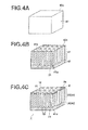
- FIG. 3 is a perspective view of a Raman spectroscopic device and Figures 4A to 4C are views showing the manufacturing steps of the Raman spectroscopic device.
- the elements analogous to those in the first embodiment will be given the same reference numerals and will not be described.
- the Raman spectroscopic device 3 in accordance with this embodiment comprises similarly to the first embodiment, in sequence from the incident side of measuring light L1, a first reflecting body 10 which exhibits semi-transmissivity/semi-reflectivity and has a surface which is a light scattering surface 3s generating a Raman scattering, a transparent body 20 and a second reflecting body 30 which has a reflectivity.
- the transparent body 20 is formed of metal oxide (Al 2 O 3 ) 41 obtained by anodic-oxidizing a part of anodic-oxidized metal (Al) 40 shown in Figure 4A and the second reflecting body 30 is formed of a non-anodic-oxidized part (Al) 42 of the anodic-oxidized metal (Al) 40.
- the second reflecting body 30 has a reflectivity.
- the transparent body 20 is a light transmitting fine hole body provided with a plurality of substantially straight fine holes 21 extending from the first reflecting body side to the second reflecting body side.
- the plurality of fine holes 21 are open at the face on first reflecting body side and are closed at the face on second reflecting body side.
- each of the plurality of fine holes 21 has a diameter smaller than the wavelength of the measuring light L1 and the plurality of fine holes 21 are arranged substantially regularly at pitches smaller than the wavelength of the measuring light L1.
- the anodic oxidation can be carried out by dipping the anodic-oxidized metal 40 (as the anode) in an electrolysis solution together with the cathode, and imparting an electric voltage across the anode and the cathode.
- the shape of the anodic-oxidized metal 40 is not limited, it is preferred that the anodic-oxidized metal 40 be like a plate or the like in shape. Those with a supporter such as those where films of anodic-oxidized metal 40 is formed on a supporting body in layers may be used.
- the cathode for instance, carbon or aluminum is used.
- an acidic electrolysis solution including but not limited to one or more of sulfuric acid, phosphoric acid, chromic acid, oxalic acid, sulfamic acid, benzensulfonic acid or amidosulfonic acid may be preferably used.
- the oxidization progresses from a surface 40s substantially in perpendicular to the surface 40s and metal oxide (Al 2 O 3 ) 41 is formed.
- the metal oxide 41 formed by the anodic oxidation is of structure where number of fine columns 41a regular hexagonal in plan are arranged without a space therebetween. At substantially the center of each fine column 41a, the fine hole 21 extending substantially straight in the direction of depth from the surface 40s opens, and the base of each fine column 41a is rounded in shape.
- the structure of the metal oxide body formed by the anodic oxidation is disclosed, for instance, in " Preparation of meso-porous Alumina by Anode Oxidation and Application thereof to functional Material” by H. Masuda, Material Technology, vol. 15, No. 10, p. 34, 1997 .
- the concentration of the electrolysis solution is 0.5M
- the temperature of the electrolysis solution is 14 to 16°C
- the electric voltage to be imparted across the anode and the cathode is 40 to 40 ⁇ 0.5 V when oxalic acid is employed as the electrolysis solution
- the fine holes 21 formed under these conditions are 5 to 200nm in diameter and 10 to 400nm in pitches.
- the first reflecting body 10 is formed by, for instance, metal deposition to the transparent body 20 and comprises a metal layer formed along the surface contour of the transparent body 20. Since, no metal film is formed in the part of the transparent body in which the fine holes 21 open, the first reflecting body 10 is of structure where number of fine metal bodies 15 each of which has a fine hole 16 at substantially the center thereof and is a regular hexagonal in plan are arranged without a space therebetween. Since fine holes 16 of the first reflecting body 10 is formed in the same pattern as the fine holes 21 of the transparent body 20, each of the plurality of fine holes 16 has a diameter smaller than the wavelength of the measuring light L1 and the plurality of fine holes 16 are arranged substantially regularly at pitches smaller than the wavelength of the measuring light L1. Even if metal is deposited on the bottom of the fine holes 21 when the first reflecting body 10 is formed, it arises no problem.
- the first reflecting body 10 exhibits a light transmissivity since it has a plurality of fine holes 16 each of which is a vacant spaces though formed of reflective metal and after all exhibits a semi-transmissivity/semi-reflectivity. Since comprising number of substantially regularly arranged fine metal bodies 15 each of which has a fine hole 16 at substantially the center thereof, is smaller than the wavelength of the measuring light L1 and is a regular hexagonal in plan, the first reflecting body 10 has an irregularity smaller than the wavelength of the measuring light L1. Since the irregularity is smaller than the wavelength of the light, the first reflecting body 10 behaves as film to light and exhibits a semi-transmissivity/semi-reflectivity having an electromagnetic mesh shielding function also in this embodiment.
- the Raman spectroscopic device 3 of this embodiment is a device where an electric field is enhanced at the light scattering surface 3s of the first reflecting body 10 to obtain the surface enhancing Raman effect and the sample can be analyzed by placing a sample or a sample cell in contact with the light scattering surface.
- the pitches of the metal bodies 15 may be any so long as they are smaller than the wavelength of the measuring light L1 and when visible light is employed as the measuring light L1, the pitches of the metal bodies 15 are preferably not larger than, for instance, 200nm. The pitches of the metal bodies 15 are preferably as small as possible.
- Spaces between adjacent fine holes 16 may be any and is preferably as small as possible.
- the width W corresponds to the width of the fine metal cable 11 and the metal particles 13 in the first and second embodiments.
- the width W is preferably not larger than an average free stroke of the electrons which are vibrated in metal by light, and specifically, the width W is preferably not larger than 50nm and more preferably not larger than 30nm.
- the second reflecting body 30 is formed of a non-anodic-oxidized part (Al) 42 of the anodic-oxidized metal (Al) 40, different from the first and second embodiments, the second reflecting body 30 is provided with a fine irregularities so that the local plasmon resonance takes place also in the second reflecting body 30 as in the first reflecting body 10.
- metal loaded on the bottom of the fine holes 21 arises no problem.
- Metal loaded on the bottom of the fine holes 21 may be deposited on the bottom of the fine holes 21 when the first reflecting body 10 is formed.
- the metal since the metal is loaded on the bottom of fine holes 21 which are formed in the fine columns 41a of the light transmissible metal oxide and are substantially regularly arranged in the device, a more effective local plasmon resonance takes place in the device and a high electric field enhancing effect can be obtained at a local plasmon resonant wavelength.
- the metal loaded on the bottom of the fine holes 21 may be any so long as it is metal as the first reflecting body, and is preferably gold (Au), silver (Ag), copper (Cu), nickel (Ni) or titanium (Ti) and gold (Au) and silver (Ag) is especially preferable.
- gold Au
- silver Au
- Cu copper
- Ni nickel
- Ti titanium
- Au gold
- the resonance As in the first embodiment, also in this embodiment, light which passes through the first reflecting body 10 and enters the transparent body 20 is repeatedly reflected between the first and second reflecting bodies 10 and 30 and a multiple interference by multiple reflection light takes place and resonates at a particular wavelength satisfying the resonant conditions.
- the resonance light at the resonant wavelength is absorbed and the electric field inside the device is enhanced and the surface enhancing Raman effect can be obtained at the light scattering surface 3s. Since the resonant wavelength changes according to the thickness and the average refractive index of the transparent body 20 as in the first embodiment, a higher surface enhancing Raman effect (for instance, not smaller than 100 times) can be obtained at a wavelength according to these factors.
- the Raman spectroscopic device 3 of this embodiment is basically the same as the first embodiment except that the transparent body 20 comprises a light transmissible fine hole member having a plurality of fine holes 21 open in the face facing the first reflecting body 10 and the first reflecting body 10 comprises a metal layer formed along the surface contour of the transparent body 20 and accordingly, exhibits the same effect as the first embodiment.
- the Raman spectroscopic device 3 of this embodiment is preferred in that a Raman spectroscopic device 3 where the fine holes 21 of the transparent body 20 and the fine holes 16 of the first reflecting body 10 are substantially regularly arranged can be easily produced. However, these fine holes may be randomly arranged.
- metal is filled in only the bottom of the fine holes 21 in this embodiment, it is possible to fill metal wholly or partly inside the fine holes 21.
- metal is wholly filled inside the fine holes 21 though no electric field enhancement by absorption of interference inside the device takes place since the first reflecting body becomes reflective, the metal particles are substantially regularly arranged on the light scattering surface 3s of the first reflecting body 10 and an effective local plasmon resonance is generated on the light scattering surface 3s, whereby the electric field is enhanced and the surface enhancing Raman effect can be obtained.
- the anodic-oxidized metal 40 used in production of the transparent body only Al is shown in this embodiment, any metal can be used so long as it can be anodic-oxidized and the metal oxide to be generated is light transmissible. Other than Al, Ti, Ta, Hf, Zr, Si, In, Zn or the like may be used.
- the anodic-oxidized metal 40 may include two or more kinds of metals which can be anodic-oxidized.
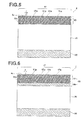
- FIG. 5 is a cross-sectional view in the direction of thickness showing a Raman spectroscopic device in accordance with a fourth embodiment of the present invention.
- the elements analogous to those in the first embodiment will be given the same reference numerals and will not be described.
- the Raman spectroscopic device 4 of this embodiment comprises similarly to the first embodiment, in sequence from the incident side of measuring light L1, a first reflecting body 10 which exhibits semi-transmissivity/semi-reflectivity and has a surface which is a light scattering surface 4s generating a Raman scattering, a transparent body 20 and a second reflecting body 30 which has a reflectivity.
- the Raman spectroscopic device in accordance with this embodiment differs from that in accordance with the first embodiment in that the first reflecting body 10 comprises a patterned metal layer in the first embodiment, the first reflecting body 10 in this embodiment comprises column structure film 17 having a number of substantially parallel columns 17p extending in a non-parallel direction to the surface 20s of the transparent body 20.
- the column structure film 17 in metal film may be any so long as it is metal and metal similar to those for the first reflecting body 10 may be shown.
- the column structure film 17 may be formed of in any method, there can be shown a gas phase growth method such as sputtering or CVD (chemical vapor deposition) .
- a number of columns 17p forming the column structure film 17 must only extend in non-parallel to the surface of the transparent body 20, the columns 17p preferably extend in the range of 90° ⁇ 15° to the surface of the transparent body 20.
- adjacent columns 17p be spaced from each other by a void 17s.
- the direction of the growth of the columns 17p be a direction but 90° in the above range. Accordingly, it is preferred that the column structure film 17 be formed by a bias sputtering.
- the column structure film 17 has light transmissivity even if it does not have a sufficient amount of void 17s.
- the thickness of the column structure film 17 may be any so long as the column structure film 17 exhibits a semi-transmissivity/semi-reflectivity.
- the length of the columns 17p may be any, when the length of the columns 17p is in the range of 30 to 500nm, the column structure film 17 can have a semi-transmissivity/semi-reflectivity with a sufficient amount of void 17s irrespective of the direction of growth of the columns 17p to the surface of the transparent body 20.
- the Raman spectroscopic device 4 of this embodiment is a device where an electric field is enhanced at the light scattering surface 4s of the first reflecting body 10 to obtain the surface enhancing Raman effect and the sample can be analyzed by placing a sample or a sample cell in contact with the light scattering surface 4s.
- the diameter r of the columns 17p and the density of the voids 17s may be any so long as the first reflecting body 10 has irregularity structure which is smaller than the wavelength of measuring light L1, when visible light is employed as the measuring light L1, the irregularity not larger than, for instance, 200nm is preferably provided to the first reflecting body 10. Also in this embodiment, since the higher the regularity in structure is, the higher in-plane uniformity of the resonant structure is, it is preferred that the voids 17s be substantially uniformly distributed.
- the diameter of the columns 17p may be any and is preferably as small as possible.
- the diameter of the columns 17p is preferably not larger than an average free stroke of the electrons which are vibrated in metal by light, and specifically, the diameter of the columns 17p is preferably not larger than 50nm and more preferably not larger than 30nm.
- the resonance As in the first embodiment, also in this embodiment, light which passes through the first reflecting body 10 and enters the transparent body 20 is repeatedly reflected between the first and second reflecting bodies 10 and 30 and a multiple interference by multiple reflection light takes place and resonates at a particular wavelength satisfying the resonant conditions.
- the resonance light at the resonant wavelength is absorbed and the electric field inside the device is enhanced and the surface enhancing Raman effect can be obtained at the light scattering surface 4s. Since the resonant wavelength changes according to the thickness and the average refractive index of the transparent body 20 as in the first embodiment, a higher surface enhancing Raman effect (for instance, not smaller than 100 times) can be obtained at a wavelength according to these factors.
- the Raman spectroscopic device 4 of this embodiment exhibits the same effect as the first embodiment.
- the first reflecting body 10 comprises a column structure film 17 where a number of substantially parallel columns 17p extend in a non-parallel direction to the surface of the transparent body and the is of metal
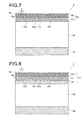
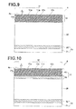
- the arrangements shown in Figures 6 to 10 may be employed.
- the arrangement where the first reflecting body 10 has a column structure film 17 and partly reflective film 18 which is formed between the column structure film 17 and the transparent body 20 and exhibits a semi-transmissivity/semi-reflectivity may be employed.
- the multiple reflection can be effectively caused in the resonator.
- the partly reflective film 18 there can be shown, for instance, metal film and dielectric multi-layered film where a dielectric body such as MgF2, SiO2 and TiO2 are laminated.
- Figures 7 and 8 show the case where the first reflecting body 10 of a Raman spectroscopic device of Figure 5 or 6 is further provided with column structure film 17 which is dielectric film and metal film 19 formed on the column structure film 17.
- the column structure film is formed by bias sputtering since the dielectric film can be formed more easily as compared with metal film and the metal film can be formed easily along the shape of the column 17p which is a dielectric body when the metal film is formed on the dielectric film having a column structure.
- the metal film 19 formed on the dielectric structural film 17 either includes a column structure or includes no column structure, the metal film 19 is formed substantially holding voids 17s formed in the column structure film 17 which is a dielectric body in either case.
- the first reflecting body 10 When being of a dielectric body, it is preferred that the first reflecting body 10 be of inorganic material which is easy to form film and is excellent in the heat resistance and in the resistance to attack by light.
- the column structure film 17 may be formed by organic material so long as the growth of the column 17p is excellent.
- plasma chemical deposition method or molecular beam deposition method As the method of forming the column structure film 17 when organic material is used, there may be shown plasma chemical deposition method or molecular beam deposition method.
- Figures 9 and 10 show the case where the second reflecting body 30 of a Raman spectroscopic device of Figure 5 or 6 is provided with a transparent body 31 and partly reflective film 32 which is formed on the transparent body 31 and exhibits a semi-transmissivity/semi-reflectivity.
- the partly reflective film 32 those which are the same as the partly reflective film 18 can be shown.
- the second reflecting body 30 can exhibit a semi-transmissivity/semi-reflectivity and it becomes possible to use light emitted from the second reflecting body 30.
- the second reflecting body 30 having such an arrangement can be applied to the Raman spectroscopic device of Figure 7 or 8 .
- the first and second reflecting bodies 10 and 30 may be changed in the arrangements thereof and the combination thereof.
- the Raman spectroscopic device of this invention may be arranged by combining the first reflecting bodies 10 of the first to third embodiments and the second reflecting bodies 30 of the first to third embodiments.
- Raman spectroscopic systems will be described with reference to Figures 11A and 11B through the example where the Raman spectroscopic device 1 of the first embodiment described above is employed.
- Figure 11A shows a Raman spectroscopic system 5 of an embodiment of the present invention.
- the Raman spectroscopic devices 2 to 4 of the second to fourth embodiment is employed, the same structure of the system may be used.
- the Raman spectroscopic system 5 of the present embodiment comprises a Raman spectroscopic device 1 of the present invention described above, a light projecting means 60 which projects measuring light L1 of a particular wavelength onto the Raman spectroscopic device 1 and a spectral means 70 which spectroscopically divides scattered light.
- the light projecting means 60 comprises a mono-wavelength light source 61 such as a laser and an optical waveguide system such as a mirror 62 which guides light emitted from the light source.
- the light projecting means 60 is arranged to project light of a particular wavelength onto a light scattering surface 1s of the Raman spectroscopic device 1 with which samples are brought into contact.
- the spectral means 70 comprises a spectral detector 71, a collecting lens 73 for collecting divergent light Ls from the sample, an optical waveguide system such as a mirror 72 which guides the divergent light Ls collected by the collecting lens 73 to the spectral detector 71 and spectroscopically divides divergent light Ls generated by the light scattering surface 1s of the Raman spectroscopic device 1 to obtain the Raman spectrum of Raman scattered light.
- the spectral means 70 is positioned to receive the scattered light generated by the light scattering surface 1s of the Raman spectroscopic device 1.
- the Raman spectroscopic device 1 when measurement is carried out with a known antibody fixed to the light scattering surface 1s of the Raman spectroscopic device 1, if an antigen is included in the sample, the obtained Raman spectrum changes due to bonding of the antibody and the antigen. Therefore, the antigen can be identified. Similarly, the antibody can be identified, by fixing a known antigen to the light scattering surface 1s.
- the sample may be brought into contact in any way, and the sample may be brought into a direct contact with the light scattering surface 1s of the Raman spectroscopic device 1, or may be filled in a sample cell 50 to be brought into contact with the light scattering surface 1s.
- Figure 11A shows a form where the sample is brought into a direct contact with the light scattering surface 1s of the Raman spectroscopic device 1
- Figure 11B shows a form where the sample is filled in a sample cell 50 and the sample cell 50 is placed on the light scattering surface 1s of the Raman spectroscopic device 1. Since, Figures 11A and 11B are the same in structure except the form in which the sample is brought into contact, the elements analogous to each other are given the same reference numerals in Figures 11A and 11B .
- the sample cell 50 may be a flow cell, and may be of any suitable material so long as it has a transparent window at an area where the measuring light L1 and the scattered light Ls passes through.
- the Raman spectroscopic system 5 of this embodiment is formed by the use of the Raman spectroscopic device 1 of this invention and the Raman scattered light is effectively enhanced, data is highly reliable and a precise Raman spectroscopy excellent in data reproduction can be carried out.
- the irregularities on the surface of the Raman spectroscopic device 1 are highly uniform, even if the light projecting place is changed for the same sample, data excellent in reproduction can be obtained. Accordingly, it is possible to increase the reliability of the data by taking a plurality of pieces of data for the same sample in different light projecting places.
- the spectral means 70 receives and spectroscopically divides only the scattered light of the non-direct-reflection components of the measuring light in the light scattering surface 1s.
- the direct-reflection components is too strong in intensity to excellently detect the Raman spectrum which is intrinsically weak. With such an arrangement, the fear can be overcome and a precise analysis can be carried out.
- Electromagnetic field analysis simulation by the FDTD method was carried out to prove the surface enhancing Raman effect thereof.
- the Raman spectroscopic device 3 of the third embodiment was employed.
- Figure 12 is a cross-sectional view in the direction of depth showing the state where a sample x is brought into contact with the Raman spectroscopic device 3 employed as a model, and in Figure 12 , one fine column is shown in an enlarged scale for the purpose of simplicity in viewing the simulating conditions. Elements analogous to those shown in Figure 3 are given the same reference numerals and are not described.
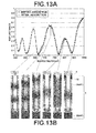
- the intensity distribution of the electric field in the device and the reflectance of the emitted light when mono-wavelength light at an arbitrary wavelength was caused to enter the first reflecting body in substantially perpendicularly thereto were calculated to prove the relation between the resonance and the electric field enhancing effect.
- Figure 13A is a graph where the reflectance of the emitted light from the surface of the device for each wavelength is plotted and represents the absorbing characteristics of the device.
- Figure 13B is a schematic view of an intensity distribution of the electric field in the device at the wavelength corresponding to each position of the spectrum shown in Figure 13A .
- the region where an especially strong electric field is generated is hatched.
- the electric field intensifies on the surface of the fine holes or the surface of the Raman spectroscopic device and it has been confirmed that, when the thickness d of the light transmissible fine hole body 41 is 400nm, the resonance takes place at wavelengths of near 420nm, 520nm and 740nm in a visible region and an effective Raman enhancing effect can be obtained.
- a local plasmon resonance is generated.
- the local plasmon resonance is generated both on the first reflecting body 10 and in the bottom of the fine holes 21. It has been confirmed from Figure 13B that the local plasmon resonance is effectively generated in the bottom of the fine holes 21 in the Raman spectroscopic device which has been employed as the model. Further, it also has been confirmed that the resonant wavelength appears at wavelengths substantially conforming the wavelength which satisfy formula (1).
- Electromagnetic field analysis simulation was carried out by the use of the Raman spectroscopic device 2 of the second embodiment as a model in a manner similar to embodiment 1 to prove the surface enhancing Raman effect thereof.
- the first reflecting body 10 comprised a metal layer where a plurality of metal particles substantially equal to each other in diameter were substantially regularly arranged in matrix on the surface of transparent body 20.
- Figure 14 shows an electron micrograph showing the surface of the first reflecting body 10 of the Raman spectroscopic device 2 employed as a model.
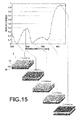
- Figure 15 shows by the use of a perspective view of the Raman spectroscopic device 2 the absorption characteristics of light emanating from the surface of the device, and the distribution of the electric field intensity in directions of the surface and the thickness of the Raman spectroscopic device 2 as in the embodiment 1. Since the arrangement of the Raman spectroscopic device 2 employed as a model in Figure 15 is shown in Figure 2 , elements analogous to those shown in Figure 2 are given the same reference numerals and are not described.
- the resonance takes place at a wavelength where the electric field intensifies near the surface. Further, it has been confirmed from Figure 16 that the electric field is effectively enhanced near the metal particles forming the first reflecting body 10.
- the technic of the present invention can be applied to the Raman spectroscopic system where scattered light obtained by projecting mono-wavelength light onto material is spectroscopically divided to obtain the Raman spectrum and is employed for, for instance, identification of the material.
Landscapes
- Health & Medical Sciences (AREA)
- Chemical & Material Sciences (AREA)
- Physics & Mathematics (AREA)
- General Health & Medical Sciences (AREA)
- Immunology (AREA)
- Pathology (AREA)
- Life Sciences & Earth Sciences (AREA)
- General Physics & Mathematics (AREA)
- Analytical Chemistry (AREA)
- Biochemistry (AREA)
- Engineering & Computer Science (AREA)
- Nuclear Medicine, Radiotherapy & Molecular Imaging (AREA)
- Crystallography & Structural Chemistry (AREA)
- Nanotechnology (AREA)
- Mathematical Physics (AREA)
- Spectroscopy & Molecular Physics (AREA)
- Theoretical Computer Science (AREA)
- Investigating, Analyzing Materials By Fluorescence Or Luminescence (AREA)
- Spectrometry And Color Measurement (AREA)
- Investigating Or Analysing Materials By Optical Means (AREA)
Abstract
A Raman spectroscopic device (1) includes an optical resonator where a first reflecting body (10) which exhibits a semi-transmissivity/semi-reflectivity and has a surface which is a light scattering surface (1s,2s,3s,4s) generating a Raman scattering, a transparent body (20) and a second reflecting body (30) which has a reflectivity are laminated in sequence one on another.
Description
- This invention relates to a Raman spectroscopic device having a function of enhancing Raman scattering and a Raman spectroscopic system using the Raman spectroscopic device.
- Raman spectroscopy is a method in which light of a mono-wavelength is projected onto a material and the obtained scattered light is spectroscopically (in a spectroscopic fashion) divided to obtain the Raman spectrum of Raman scattered light and is employed for, for instance, identification of the material. Since the Raman scattered light is weak, there has been developed surface enhancing Raman device where the Raman scattering is enhanced on the surface. As one of the surface enhancing Raman devices, a device using a local plasmon resonance can be shown. This device is based on the fact that when light is projected onto a metal body, especially a metal body having an irregularity of an order of nanometer, in a state where the material is in contact with the metal body, an electric field is enhanced by a local plasmon resonance and the intensity of the Raman scattered light of the sample in contact with the metal body is enhanced. It is said as the regularity of the fine structure of the metal body is higher, an electric field enhancement which is more uniform and more effective can be obtained.
- As one of methods of producing a fine irregularity structure on the surface of metal body, a method where metal particles highly uniform in particle diameters are prepared and the metal particles is randomly fixed to the surface of the metal body can be shown. In Japanese Unexamined Patent Publication No.
2003-49205 - In Japanese Unexamined Patent Publication No.
2005-172569 - However, the method disclosed in Japanese Unexamined Patent Publication No.
2003-49205 2003-49205 - In a fine structure disclosed in Japanese Unexamined Patent Publication No.
2005-172569 - In view of the foregoing observations and description, the primary object of the present invention is to provide a Raman spectroscopic device in which the Raman effect enhancing wavelength can be more simply controlled as compared with the surface enhancing Raman device using local plasmon resonance and a Raman spectroscopic system using the Raman spectroscopic device.
- In accordance with the present invention, there is provided a Raman spectroscopic device for use in Raman spectroscopy where measuring light of a particular wavelength is projected onto a sample in contact with a light scattering surface and the obtained Raman scattered light generated in the light scattering surface is spectroscopically (in a spectroscopic fashion) divided and is employed for, for instance, detecting a material in the sample comprising an optical resonator where a first reflecting body which exhibits a semi-transmissivity/semi-reflectivity and has a surface which is the light scattering surface, a transparent body and a second reflecting body which has a reflectivity are superposed in sequence one on another, whereby the intensity of the Raman scattered light is enhanced by the electric field enhanced in the light scattering surface by light absorption generated by a resonance in the optical resonator upon projection of the measuring light.
- In this specification, the "semi-transmissivity/semi-reflectivity" means to have both the transmissivity and the reflectivity irrespective of the transmittance and the reflectance.
- In the Raman spectroscopic device of the present invention, it is preferred that the first reflecting body has irregularity structure which is smaller than the wavelength of the measuring light to be projected onto the light scattering surface.
- The expression "irregularity structure which is smaller than the wavelength of the measuring light" as used here means that the average size (the "size" as used here means "a maximum width") of the projections and the recessed parts (the "recessed parts" as used here includes a space extending through the reflecting body in the direction of thickness) and the average pitches of the projections and the recessed parts are smaller than the wavelength of the measuring light.
- As a preferred embodiment of the Raman spectroscopic device of the present invention, there can be shown that in which the first reflecting body is a metal layer formed in a pattern on the surface of the transparent body.
- As another preferred embodiment of the Raman spectroscopic device of the present invention, there can be shown that in which the first reflecting body is a metal layer comprising a plurality of non-aggregate metal particles fixed to the surface of the transparent body.
- In this specification, the "non-aggregate metal particles" is defined to be metal particles included in either one of (1) those where the metal particles are spaced from each other without associating with each other and (2) those where the metal particles are a single particle after they bond together and never returns to the original state.
- As still another preferred embodiment of the Raman spectroscopic device of the present invention, there can be shown that in which the transparent body comprises a transparent fine hole body having a plurality of fine holes which open in a surface opposed to the first reflecting body and is smaller than the wavelength of the measuring light in diameter and the first reflecting body is a metal layer having a plurality of fine holes along the surface of the transparent body. In such a structure, at least a part of the fine holes may be filled with metal or only a bottom of the fine holes may be filled with metal.
- As still another preferred embodiment of the Raman spectroscopic device of the present invention, there can be shown that where the first reflecting body comprises metal column structure film having a number of substantially parallel columns extending in a non-parallel direction to the surface of the transparent body.
- As still another preferred embodiment of the Raman spectroscopic device of the present invention, there can be shown that where the first reflecting body comprises dielectric column structure film having a number of substantially parallel columns extending in a non-parallel direction to the surface of the transparent body and metal film formed on the dielectric column structure film.
- The Raman spectroscopic system of the present invention comprises a Raman spectroscopic device of the present invention described above, a light projecting means which projects light of a particular wavelength onto the light scattering surface of the Raman spectroscopic device and a spectral means which spectroscopically divides the light scattered by the light scattering surface, thereby obtaining spectrum of Raman scattered light.
- Since the Raman spectroscopic device of the present invention comprises an optical resonator where the first reflecting body which exhibits semi-transmissivity/semi-reflectivity and has a surface which is a light scattering surface generating a Raman scattering, the transparent body and the second reflecting body which has a reflectivity are superposed in sequence one on another, and light traveling into the transparent body after transmitted by the first reflecting body repeats reflection between the first and second reflecting bodies to generate multiple reflection, whereby a multiple interference by the light reflected in the multiple reflection effectively takes place and the electric field of the optical resonator is enhanced at the resonant wavelength by the resonance generated by the multiple interference. Accordingly, the surface enhancing Raman effect is effectively obtained in the surface of the first reflecting body which is a light scattering surface.
- Further, since in the Raman spectroscopic device of the present invention, the resonating wavelength changes according to the average refractive index and the thickness of the transparent body, and the Raman effect enhancing wavelength can be controlled by a simple design change where these factors are only changed. Accordingly, in accordance with the present invention, it is possible to obtain the Raman spectroscopic device having the surface enhancing Raman effect at a desired wavelength according to the application by a simple design change.
-
-
Figure 1A is a perspective view of a Raman spectroscopic device in accordance with a first embodiment of the present invention, -
Figure 1B is a cross-sectional view of the same, -
Figure 2A is a perspective view of a Raman spectroscopic device in accordance with a second embodiment of the present invention, -
Figure 2B is a plan view of the same, -
Figure 3 is a perspective view of a Raman spectroscopic device in accordance with a third embodiment of the present invention, -
Figures 4A to 4C are views showing the process of producing the Raman spectroscopic device shown inFigure 3 , -
Figure 5 is a cross-sectional view in the direction of thickness showing a Raman spectroscopic device in accordance with a fourth embodiment of the present invention, -
Figure 6 is a cross-sectional view in the direction of thickness showing a Raman spectroscopic device in another preferred form of a fourth embodiment of the present invention, -
Figure 7 is a cross-sectional view in the direction of thickness showing a Raman spectroscopic device in still another preferred form of a fourth embodiment of the present invention, -
Figure 8 is a cross-sectional view in the direction of thickness showing a Raman spectroscopic device in still another preferred form of a fourth embodiment of the present invention, -
Figure 9 is a cross-sectional view in the direction of thickness showing a Raman spectroscopic device in still another preferred form of a fourth embodiment of the present invention, -
Figure 10 is a cross-sectional view in the direction of thickness showing a Raman spectroscopic device in still another preferred form of a fourth embodiment of the present invention, -
Figure 11A is a view briefly showing a Raman spectroscopic system in accordance with an embodiment of the present invention, -
Figure 11B is a view showing an example of contact of the sample with the Raman spectroscopic device in the Raman spectroscopic system ofFigure 11A , -
Figure 12 is an enlarged cross-sectional view showing the Ramanspectroscopic device 3 employed as a model of simulation of theembodiment 1, -
Figure 13A is a view showing the light emanation/absorption characteristics ofembodiment 1, -
Figure 13B is a view showing the electric field intensity distribution in the fine hole at the absorption peak wavelength shown inFigure 13A , -
Figure 14 is an electron micrograph showing the Ramanspectroscopic device 2 employed as a model of simulation of theembodiment 2, -
Figure 15 is a perspective view of the Ramanspectroscopic device 2 showing the light emanation/absorption characteristics and the distribution of the electric field intensity in the directions of the surface and the thickness at each absorption peak wavelength of theembodiment 2, and -
Figure 16 is a plan view of the Ramanspectroscopic device 2 showing the distribution of the electric field intensity at the local plasmon resonance wavelength. - A Raman spectroscopic device in accordance with a first embodiment of the present invention will be described with reference to
Figures 1A and 1B , hereinbelow.Figure 1A is a perspective of the first embodiment andFigure 1B is a cross-sectional view of the same (taken along line A-A'). - As shown in
Figures 1A and 1B , the Ramanspectroscopic device 1 in accordance with this embodiment comprises in sequence, from the incident side (from upward inFigures 1A and 1B ) of measuring light L1, a first reflectingbody 10 which exhibits semi-transmissivity/semi-reflectivity and has a surface which is alight scattering surface 1s generating a Raman scattering, atransparent body 20 and a second reflectingbody 30 which has a reflectivity. The measuring light L1 is mono-wavelength light and the wavelength of the measuring light L1 is selected according to the material to be detected. - The
transparent body 20 comprises a transparent flat substrate while the firstreflecting body 10 comprises a metal layer wherefine metal cable 11 is formed in a regular grid pattern on one side of thetransparent body 20 and the second reflectingbody 30 comprises a solid metal layer where fine metal formed on the other side of thetransparent body 20. - The
transparent body 20 may be formed of any suitable material, and for instance, may be formed of a transparent ceramics such as glass or alumina or a transparent resin such as acrylic resin or polycarbonate resin. - The first and second
reflecting bodies reflecting bodies - The second reflecting
body 30 which is a solid metal layer can be formed by, for instance, a metal vapor deposition. - The first reflecting
body 10 can be formed, for instance, by carrying out the known photolithography after a solid metal layer is formed by, for instance, the metal vapor deposition. - The first reflecting
body 10 exhibits a light transmissivity since it has a plurality of patternedspaces 12 though formed of reflective metal and after all exhibits a semi-transmissivity/semi-reflectivity. The line width and the pitches of thefine metal cable 11 of the first reflectingbody 10 are smaller than the wavelength of the measuring light L1, and the first reflectingbody 10 has an irregularity smaller than the wavelength of the measuring light L1. When the irregularity is smaller than the wavelength of the light, the first reflectingbody 10 behaves as film to light and exhibits a semi-transmissivity/semi-reflectivity having an electromagnetic mesh shielding function. - The Raman spectroscopic device in accordance with this embodiment is a device having a surface enhancing Raman effect, where the electric field is strengthened on the
light scattering surface 1s of the first reflectingbody 10, and the sample can be analyzed by placing a sample or a sample cell in contact with thelight scattering surface 1s. - The pitches of the
fine metal cable 11 may be any so long as they are smaller than the wavelength of the measuring light L1 and when visible light is employed as the measuring light L1, the pitches of thefine metal cable 11 are preferably not larger than, for instance, 200nm. The pitches of thefine metal cable 11 are preferably as small as possible. The line width of thefine metal cable 11 may be any so long as it is smaller than the wavelength of the measuring light L1 and the line width of thefine metal cable 11 is preferably as small as possible. The line width of thefine metal cable 11 is preferably not larger than an average free stroke of the electrons which are vibrated by light, and specifically, the line width of thefine metal cable 11 is preferably not larger than 50nm and more preferably not larger than 30nm. - The thickness of the
transparent body 20 may be any, and preferably not larger than 300nm in that absorption peak wavelength in a visible wavelength region by the multiple interference is a single and easy to detect, while preferably not smaller than 100nm in that a multiple interference effectively takes place, and absorption peak wavelengths by the multiple interference are easy to detect in a visible wavelength region. - In the Raman spectroscopic device in accordance with this embodiment, the resonant wavelength can be changed according to a thickness of the
transparent body 20 and an average refractive index in thetransparent body 20. A thickness of thetransparent body 20, an average refractive index in thetransparent body 20 and the resonant wavelength substantially satisfies the following formula (1), and accordingly, when the Raman spectroscopic devices are the same in the average refractive index in thetransparent body 20, the resonant wavelength can be changed by only changing the thickness of thetransparent body 20.
wherein d represents the thickness of thetransparent body 20, λ represents the resonant wavelength, n represents the average refractive index in thetransparent body 20 and m represents an integer. - When the
transparent body 20 comprises a light transmitting fine hole member as in the third embodiment described later, "the average refractive index in thetransparent body 20" means the average of the refractive index in the light transmitting fine hole member and the refractive index of the material in the fine holes (when the fine holes are not filled with a particular material, "the material in the fine holes" is air, and when the fine holes are filled with a particular material, "the material in the fine holes" is the particular material in the fine holes and/or a mixture of air and the particular material in the fine holes.) - Further, though the refractive index is represented by a complex refractive index when the material absorbs light, since the complex part is 0 in the
transparent body 20 and even when thetransparent body 20 has fine holes, the influence by the material in the fine holes is small, the formula (1) is shown as a simple refractive index without a complex part. - Though varies depending upon the physical properties and/or the surface state of the first and second reflecting
bodies transparent body 20 and the average refractive index in thetransparent body 20, the resonant wavelength can be determined in a precision of order of several nm according to the above formula (1). - As shown in
Figure 1B , when the measuring light L1 impinges upon theRaman spectroscopic device 1, the measuring light L1 is partly reflected by the surface of the first reflecting body 10 (not shown) and partly passes through the first reflectingbody 10 to enter thetransparent body 20 according to the transmissivity or the reflectance of the first reflectingbody 10. Light entering thetransparent body 20 is repeatedly reflected between the first and second reflectingbodies Raman spectroscopic device 1 is of resonant structure where a multiple reflection takes place between the first and second reflectingbodies transparent body 20 and resonates at a particular wavelength satisfying the resonant conditions to exhibit an absorption characteristics where the light at the resonant wavelength is absorbed. Then, emanation light L2 different from the measuring light L1 in the physical properties is emanated according to the absorption characteristics. Further, inside the device, the electric field is enhanced according to the absorption characteristics and the surface enhancing Raman effect can be obtained at thelight scattering surface 1s. - In the
Raman spectroscopic device 1, it is preferred that the device structure is formed by taking an optical impedance matching so that the number of the multiple reflection (finesse) in thetransparent body 20 is maximized. Such arrangement is preferable in that the absorption peaks become sharp and a more effective Raman enhancing can be obtained. - In the Raman spectroscopy, it is necessary to change the wavelength of the measuring light to be projected onto a sample according to the sample and in a Raman spectroscopic device where the Raman enhancing wavelength is caused to conform to the wavelength of the measuring light, an effective surface enhancing Raman effect can be obtained. Accordingly, it is preferred to design a Raman spectroscopic device according to the wavelength of the measuring light. However, control of the Raman enhancing wavelength requires complicated process, for instance, in the case of a surface enhancing Raman spectroscopic device using local plasmon resonance since a precise control of the size of the fine structure of metal is necessary.
- In the
Raman spectroscopic device 1 of this embodiment, since the resonant wavelength changes according to the thickness and the average refractive index of thetransparent body 20 as shown in formula (1), the Raman effect enhancing wavelength can be controlled by a simple design change where these factors are only changed. Accordingly, in accordance with this embodiment, the Raman spectroscopic device which has the surface enhancing Raman effect at a desired wavelength according to the application thereof can be easily obtained without a complicated device design. - In the
Raman spectroscopic device 1 of this embodiment, since a multiple interference effectively takes place and a strong absorption to light of a particular wavelength takes place, the surface enhancing Raman effect is larger than the Raman spectroscopic device using local plasmon resonance (for instance, not smaller than 100 times) and a high-precision analysis can be realized. - In the
Raman spectroscopic device 1 of this embodiment, since further the first reflectingbody 10 is of metal having free electrons and the first reflectingbody 10 has an irregularity smaller than the wavelength of the measuring light L1, local plasmon resonance can take place in the first reflectingbody 10. - Local plasmon resonance is a phenomenon where the free electrons of metal resonate with the electric field of light and an electric field is generated. It is said that especially in a metal layer having a fine irregularity, a strong electric field is generated around projections when free electrons on the projections resonate with the electric field of light and vibrates and the local plasmon resonance effectively takes place. In this embodiment, since the first reflecting
body 10 has an irregularity smaller than the wavelength of the measuring light L1 as described above, the local plasmon resonance effectively takes place. - At the wavelength where the local plasmon resonance is generated, scattering and/or absorption of the measuring light L1 is significantly enhanced, and the electric field is enhanced at the
light scattering surface 1s as the resonance by the above multiple interference. The wavelength where the local plasmon resonance is generated (resonance peak wavelength) and the degree of scattering and/or absorption of the measuring light L1 depend upon the size of irregularity on the surface of theRaman spectroscopic device 1, the kind of metal, the refractive index of the sample in contact with the surface and the like. - The absorption peaks by the multiple interference and by the local plasmon resonance appear sometimes at different wavelengths and sometimes at a wavelength.
- Though the first and second reflecting
bodies body 10 is formed of metal is preferable in that the surface enhancing Raman effect by the local plasmon resonance can also be obtained. - In this embodiment, both the resonance by the multiple interference and the local plasmon resonance are generated and the surface enhancing Raman effects generated by phenomena independent of each other are obtained as described above. However, it is conceivable that the surface enhancing Raman effect is enhanced by mutual action of these phenomena or a phenomenon peculiar to the structure of the device described above.
- Though the case where the first reflecting
body 10 is in a regular grid pattern has been described in this embodiment, the first reflectingbody 10 is in any pattern and it may be even in a random pattern. However, that the regularity in structure is higher is preferred in that higher the in-plane uniformity of the resonant structure is, and the characteristics are more concentrated. - A Raman spectroscopic device of a second embodiment of the present invention will be described with reference to
Figures 2A and 2B , hereinbelow.Figure 2A is a perspective view similar toFigure 1A of the first embodiment andFigure 2B is a plan view of a Raman spectroscopic device. In this embodiment, the elements analogous to those in the first embodiment will be given the same reference numerals and will not be described. - As shown in
Figures 2A and 2B , theRaman spectroscopic device 2 in accordance with this embodiment comprises similarly to the first embodiment, in sequence from the incident side of measuring light L1, a first reflectingbody 10 which exhibits semi-transmissivity/semi-reflectivity and has a surface which is alight scattering surface 2s generating a Raman scattering, atransparent body 20 and a second reflectingbody 30 which has a reflectivity. - The
Raman spectroscopic device 2 in accordance with this embodiment differs from that in accordance with the first embodiment in that the first reflectingbody 10 is formed of a plurality ofnon-aggregate metal particles 13 of substantially the same diameters which are regularly arranged in matrix on the surface of thetransparent body 20 and fixed there, whereas the first reflectingbody 10 in the first embodiment is a metal layer formed in a pattern. - In this embodiment, similarly to the first embodiment that the regularity in structure is higher is preferred in that higher the in-plane uniformity of the resonant structure is, and the characteristics are more concentrated. When the
metal particles 13 includes aggregate metal particles, the first reflecting body is formed of partly aggregate metal particles where a number of metal particles aggregate and partly non-aggregate metal particles and the regularity in structure of the first reflecting body is apt to be lowered. Whereas, since themetal particles 13 are non-aggregate metal particles in this embodiment, the first reflectingbody 10 can be easily higher in uniformity of the structure as compared with when themetal particles 13 includes aggregate metal particle. - The
metal particles 13 may be formed of any suitable, and, for instance, it may be formed of the same metal for the first reflectingbody 10 of the first embodiment. - Further, since the
metal particles 13 are non-aggregate metal particles, as previously mentioned, they belong to either one of (1) those where the metal particles are spaced from each other without associating with each other and (2) those where the metal particles are a single particle after they bond together and never returns to the original state. - As the first reflecting
body 10 comprising a metal layer formed by a plurality ofsecured metal particles 13 defined in (1), there can be shown a metal layer where a plurality ofmetal particles 13 are arranged so that they are spaced from each other by a distance not smaller than a predetermined distance not to associate with each other. In this metal layer, themetal particles 13 may be either randomly or substantially regularly arranged. - As a metal layer where the
metal particles 13 are randomly arranged, there can be shown a metal layer which is formed in an island pattern by a bias sputtering. - As a metal layer where the
metal particles 13 are substantially regularly arranged, there can be shown those wheremetal particles 13 which are like a dot, mesh, or a needle or in a bow-tie array are patterned to be substantially regularly arranged. Patterning in these cases can be realized, for instance, by a method like lithography, or focusing ion beam method (FIB method) using processing or self-organizing. - As the first reflecting
body 10 where a plurality ofmetal particles 13 are secured as defined in (2), there can be shown those wheremetal particles 13 are integrated in the step of metal growth by fusion or plating and cannot be returned to the state before integration. - Further, the first reflecting
body 10 can be formed by, for instance, applying dispersion of themetal particles 13 by spin coating or the like to the surface of thetransparent body 20, and drying it. It is preferred that the dispersion includes a binder such as resin or protein so that themetal particles 13 are fixed to the surface of thetransparent body 20 by way of the binder. When protein is employed as the binder, it is possible to fix themetal particles 13 to the surface of thetransparent body 20 by the use of the bonding reaction between the proteins. - The first reflecting
body 10 exhibits a light transmissivity since it has a plurality ofinter-particle spaces 14 which are void though formed of reflective metal and after all exhibits a semi-transmissivity/semi-reflectivity. The diameter and the pitch of themetal particles 13 are designed to be smaller than the wavelength of the measuring light L1, and the first reflectingbody 10 has an irregularity smaller than the wavelength of the measuring light L1. Since being smaller than the wavelength of the light, the first reflectingbody 10 behaves as film to light and exhibits a semi-transmissivity/semi-reflectivity having an electromagnetic mesh shielding function also in this embodiment. - Also the
Raman spectroscopic device 2 of this embodiment is a device where an electric field is enhanced at thelight scattering surface 2s of the first reflectingbody 10 to obtain the surface enhancing Raman effect and the sample can be analyzed by placing a sample or a sample cell in contact with thelight scattering surface 2s. - The pitches of the
metal particles 13 may be any so long as they are smaller than the wavelength of the measuring light L1 and when visible light is employed as the measuring light L1, the pitches of themetal particles 13 are preferably not larger than, for instance, 200nm. The pitches of themetal particles 13 are preferably as small as possible. The diameter of themetal particles 13 may be any and the diameter of themetal particles 13 is preferably as small as possible. The diameter of themetal particles 13 is preferably not larger than an average free stroke of the electrons which are vibrated in metal by light, and specifically, the diameter of themetal particles 13 is preferably not larger than 50nm and more preferably not larger than 30nm. - As in the first embodiment, also in this embodiment, light which passes through the first reflecting
body 10 and enters thetransparent body 20 is repeatedly reflected between the first and second reflectingbodies light scattering surface 2s. In theRaman spectroscopic device 1 of this embodiment, since the resonant wavelength changes according to the thickness and the average refractive index of thetransparent body 20 as in the first embodiment, a higher surface enhancing Raman effect (for instance, not smaller than 100 times) can be obtained at a wavelength according to these factors. - The
Raman spectroscopic device 1 of this embodiment is basically the same as the first embodiment except that the first reflectingbody 10 is of the metal particle layer and accordingly, exhibits the same effect as the first embodiment. - Though the case where the first reflecting
body 10 comprises a metal layer where a plurality of substantially the same diameter metal particles are regularly arranged in a matrix has been described in this embodiment, the first reflectingbody 10 may be distributed and may be in any pattern. The first reflectingbody 10 may be even in a random pattern. - A Raman spectroscopic device of a third embodiment of the present invention will be described with reference to
Figures 3 and4A to 4C , hereinbelow.Figure 3 is a perspective view of a Raman spectroscopic device andFigures 4A to 4C are views showing the manufacturing steps of the Raman spectroscopic device. In this embodiment, the elements analogous to those in the first embodiment will be given the same reference numerals and will not be described. - As shown in
Figure 3 , theRaman spectroscopic device 3 in accordance with this embodiment comprises similarly to the first embodiment, in sequence from the incident side of measuring light L1, a first reflectingbody 10 which exhibits semi-transmissivity/semi-reflectivity and has a surface which is alight scattering surface 3s generating a Raman scattering, atransparent body 20 and a second reflectingbody 30 which has a reflectivity. - In this embodiment, different from the first embodiment, the
transparent body 20 is formed of metal oxide (Al2O3) 41 obtained by anodic-oxidizing a part of anodic-oxidized metal (Al) 40 shown inFigure 4A and the second reflectingbody 30 is formed of a non-anodic-oxidized part (Al) 42 of the anodic-oxidized metal (Al) 40. The second reflectingbody 30 has a reflectivity. - In this embodiment, the
transparent body 20 is a light transmitting fine hole body provided with a plurality of substantially straight fine holes 21 extending from the first reflecting body side to the second reflecting body side. The plurality offine holes 21 are open at the face on first reflecting body side and are closed at the face on second reflecting body side. In thetransparent body 20, each of the plurality offine holes 21 has a diameter smaller than the wavelength of the measuring light L1 and the plurality offine holes 21 are arranged substantially regularly at pitches smaller than the wavelength of the measuring light L1. - The anodic oxidation can be carried out by dipping the anodic-oxidized metal 40 (as the anode) in an electrolysis solution together with the cathode, and imparting an electric voltage across the anode and the cathode. Though the shape of the anodic-oxidized
metal 40 is not limited, it is preferred that the anodic-oxidizedmetal 40 be like a plate or the like in shape. Those with a supporter such as those where films of anodic-oxidizedmetal 40 is formed on a supporting body in layers may be used. As the cathode, for instance, carbon or aluminum is used. As the electrolysis solution, an acidic electrolysis solution including but not limited to one or more of sulfuric acid, phosphoric acid, chromic acid, oxalic acid, sulfamic acid, benzensulfonic acid or amidosulfonic acid may be preferably used. - As shown in
Figures 4A to 4C , when anodic-oxidizing anodic-oxidizedmetal 40, the oxidization progresses from asurface 40s substantially in perpendicular to thesurface 40s and metal oxide (Al2O3) 41 is formed. Themetal oxide 41 formed by the anodic oxidation is of structure where number offine columns 41a regular hexagonal in plan are arranged without a space therebetween. At substantially the center of eachfine column 41a, thefine hole 21 extending substantially straight in the direction of depth from thesurface 40s opens, and the base of eachfine column 41a is rounded in shape. The structure of the metal oxide body formed by the anodic oxidation is disclosed, for instance, in "Preparation of meso-porous Alumina by Anode Oxidation and Application thereof to functional Material" by H. Masuda, Material Technology, vol. 15, No. 10, p. 34, 1997. - As suitable conditions under which the anode-oxidation is to be carried out to form the regularly arranged
metal oxide body 41, conditions that the concentration of the electrolysis solution is 0.5M, the temperature of the electrolysis solution is 14 to 16°C, and the electric voltage to be imparted across the anode and the cathode is 40 to 40±0.5 V when oxalic acid is employed as the electrolysis solution can be shown. The fine holes 21 formed under these conditions are 5 to 200nm in diameter and 10 to 400nm in pitches. - In this embodiment, the first reflecting
body 10 is formed by, for instance, metal deposition to thetransparent body 20 and comprises a metal layer formed along the surface contour of thetransparent body 20. Since, no metal film is formed in the part of the transparent body in which the fine holes 21 open, the first reflectingbody 10 is of structure where number offine metal bodies 15 each of which has afine hole 16 at substantially the center thereof and is a regular hexagonal in plan are arranged without a space therebetween. Since fine holes 16 of the first reflectingbody 10 is formed in the same pattern as the fine holes 21 of thetransparent body 20, each of the plurality offine holes 16 has a diameter smaller than the wavelength of the measuring light L1 and the plurality offine holes 16 are arranged substantially regularly at pitches smaller than the wavelength of the measuring light L1. Even if metal is deposited on the bottom of the fine holes 21 when the first reflectingbody 10 is formed, it arises no problem. - The first reflecting
body 10 exhibits a light transmissivity since it has a plurality offine holes 16 each of which is a vacant spaces though formed of reflective metal and after all exhibits a semi-transmissivity/semi-reflectivity. Since comprising number of substantially regularly arrangedfine metal bodies 15 each of which has afine hole 16 at substantially the center thereof, is smaller than the wavelength of the measuring light L1 and is a regular hexagonal in plan, the first reflectingbody 10 has an irregularity smaller than the wavelength of the measuring light L1. Since the irregularity is smaller than the wavelength of the light, the first reflectingbody 10 behaves as film to light and exhibits a semi-transmissivity/semi-reflectivity having an electromagnetic mesh shielding function also in this embodiment. - Also the
Raman spectroscopic device 3 of this embodiment is a device where an electric field is enhanced at thelight scattering surface 3s of the first reflectingbody 10 to obtain the surface enhancing Raman effect and the sample can be analyzed by placing a sample or a sample cell in contact with the light scattering surface. - The pitches of the metal bodies 15 (pitches of the fine holes 16) may be any so long as they are smaller than the wavelength of the measuring light L1 and when visible light is employed as the measuring light L1, the pitches of the
metal bodies 15 are preferably not larger than, for instance, 200nm. The pitches of themetal bodies 15 are preferably as small as possible. - Spaces between adjacent fine holes 16 (the width W of
metal bodies 15 between adjacent fine holes 16) may be any and is preferably as small as possible. The width W corresponds to the width of thefine metal cable 11 and themetal particles 13 in the first and second embodiments. The width W is preferably not larger than an average free stroke of the electrons which are vibrated in metal by light, and specifically, the width W is preferably not larger than 50nm and more preferably not larger than 30nm. - In the
Raman spectroscopic device 3 of this embodiment, since the second reflectingbody 30 is formed of a non-anodic-oxidized part (Al) 42 of the anodic-oxidized metal (Al) 40, different from the first and second embodiments, the second reflectingbody 30 is provided with a fine irregularities so that the local plasmon resonance takes place also in the second reflectingbody 30 as in the first reflectingbody 10. - In the
Raman spectroscopic device 3 of this embodiment, metal loaded on the bottom of the fine holes 21 arises no problem. Metal loaded on the bottom of the fine holes 21 may be deposited on the bottom of the fine holes 21 when the first reflectingbody 10 is formed. In this case, since the metal is loaded on the bottom offine holes 21 which are formed in thefine columns 41a of the light transmissible metal oxide and are substantially regularly arranged in the device, a more effective local plasmon resonance takes place in the device and a high electric field enhancing effect can be obtained at a local plasmon resonant wavelength. - The metal loaded on the bottom of the fine holes 21 may be any so long as it is metal as the first reflecting body, and is preferably gold (Au), silver (Ag), copper (Cu), nickel (Ni) or titanium (Ti) and gold (Au) and silver (Ag) is especially preferable. In this case, since a local plasmon resonance takes place on the surface of the first reflecting body and on the bottom of the fine holes 21, it is preferred that metal loaded on the bottom of the fine holes 21 be of the same kind as the metal of the first reflecting body in order to obtain a more effective local plasmon resonance.
- As in the first embodiment, also in this embodiment, light which passes through the first reflecting
body 10 and enters thetransparent body 20 is repeatedly reflected between the first and second reflectingbodies light scattering surface 3s. Since the resonant wavelength changes according to the thickness and the average refractive index of thetransparent body 20 as in the first embodiment, a higher surface enhancing Raman effect (for instance, not smaller than 100 times) can be obtained at a wavelength according to these factors. - Further in this embodiment, since an effective local plasmon resonance takes place at the bottoms of the fine holes 21, a surface enhancing Raman effect by a higher local plasmon resonance as compared with the Raman spectroscopic devices of the first and second embodiments can be obtained.
- The
Raman spectroscopic device 3 of this embodiment is basically the same as the first embodiment except that thetransparent body 20 comprises a light transmissible fine hole member having a plurality offine holes 21 open in the face facing the first reflectingbody 10 and the first reflectingbody 10 comprises a metal layer formed along the surface contour of thetransparent body 20 and accordingly, exhibits the same effect as the first embodiment. - Since being produced on the basis of the anodic oxidation, the
Raman spectroscopic device 3 of this embodiment is preferred in that aRaman spectroscopic device 3 where the fine holes 21 of thetransparent body 20 and the fine holes 16 of the first reflectingbody 10 are substantially regularly arranged can be easily produced. However, these fine holes may be randomly arranged. - Though metal is filled in only the bottom of the fine holes 21 in this embodiment, it is possible to fill metal wholly or partly inside the fine holes 21. When metal is wholly filled inside the fine holes 21, though no electric field enhancement by absorption of interference inside the device takes place since the first reflecting body becomes reflective, the metal particles are substantially regularly arranged on the
light scattering surface 3s of the first reflectingbody 10 and an effective local plasmon resonance is generated on thelight scattering surface 3s, whereby the electric field is enhanced and the surface enhancing Raman effect can be obtained. - Though as a main component of the anodic-oxidized
metal 40 used in production of the transparent body, only Al is shown in this embodiment, any metal can be used so long as it can be anodic-oxidized and the metal oxide to be generated is light transmissible. Other than Al, Ti, Ta, Hf, Zr, Si, In, Zn or the like may be used. The anodic-oxidizedmetal 40 may include two or more kinds of metals which can be anodic-oxidized. - A Raman spectroscopic device of a fourth embodiment of the present invention will be described with reference to
Figure 5 , hereinbelow.Figure 5 is a cross-sectional view in the direction of thickness showing a Raman spectroscopic device in accordance with a fourth embodiment of the present invention. In this embodiment, the elements analogous to those in the first embodiment will be given the same reference numerals and will not be described. - As shown in
Figure 5 , theRaman spectroscopic device 4 of this embodiment comprises similarly to the first embodiment, in sequence from the incident side of measuring light L1, a first reflectingbody 10 which exhibits semi-transmissivity/semi-reflectivity and has a surface which is alight scattering surface 4s generating a Raman scattering, atransparent body 20 and a second reflectingbody 30 which has a reflectivity. - The Raman spectroscopic device in accordance with this embodiment differs from that in accordance with the first embodiment in that the first reflecting
body 10 comprises a patterned metal layer in the first embodiment, the first reflectingbody 10 in this embodiment comprisescolumn structure film 17 having a number of substantiallyparallel columns 17p extending in a non-parallel direction to thesurface 20s of thetransparent body 20. - The
column structure film 17 in metal film may be any so long as it is metal and metal similar to those for the first reflectingbody 10 may be shown. Thecolumn structure film 17, though it is metal film, exhibits a light transmissivity since it has a plurality of vacant spaces betweenadjacent columns 17p and after all exhibits a semi-transmissivity/semi-reflectivity. Since the diameter r of the column and the density of the vacant spaces have been designed so that the first reflectingbody 10 has irregularity structure which is smaller than the wavelength of measuring light L1. Accordingly, the first reflectingbody 10 behaves as film to light and exhibits a semi-transmissivity/semi-reflectivity having an electromagnetic mesh shielding function. - Though the
column structure film 17 may be formed of in any method, there can be shown a gas phase growth method such as sputtering or CVD (chemical vapor deposition) . Though a number ofcolumns 17p forming thecolumn structure film 17 must only extend in non-parallel to the surface of thetransparent body 20, thecolumns 17p preferably extend in the range of 90°±15° to the surface of thetransparent body 20. As described above, it is preferred thatadjacent columns 17p be spaced from each other by a void 17s. When thecolumn structure film 17 is formed of in above described method, it is further preferred that the direction of the growth of thecolumns 17p be a direction but 90° in the above range. Accordingly, it is preferred that thecolumn structure film 17 be formed by a bias sputtering. However, when the thickness of the film is sufficiently small, thecolumn structure film 17 has light transmissivity even if it does not have a sufficient amount of void 17s. - The thickness of the
column structure film 17 may be any so long as thecolumn structure film 17 exhibits a semi-transmissivity/semi-reflectivity. Though the length of thecolumns 17p may be any, when the length of thecolumns 17p is in the range of 30 to 500nm, thecolumn structure film 17 can have a semi-transmissivity/semi-reflectivity with a sufficient amount of void 17s irrespective of the direction of growth of thecolumns 17p to the surface of thetransparent body 20. - Also the
Raman spectroscopic device 4 of this embodiment is a device where an electric field is enhanced at thelight scattering surface 4s of the first reflectingbody 10 to obtain the surface enhancing Raman effect and the sample can be analyzed by placing a sample or a sample cell in contact with thelight scattering surface 4s. - Though the diameter r of the
columns 17p and the density of thevoids 17s may be any so long as the first reflectingbody 10 has irregularity structure which is smaller than the wavelength of measuring light L1, when visible light is employed as the measuring light L1, the irregularity not larger than, for instance, 200nm is preferably provided to the first reflectingbody 10. Also in this embodiment, since the higher the regularity in structure is, the higher in-plane uniformity of the resonant structure is, it is preferred that thevoids 17s be substantially uniformly distributed. - The diameter of the
columns 17p may be any and is preferably as small as possible. The diameter of thecolumns 17p is preferably not larger than an average free stroke of the electrons which are vibrated in metal by light, and specifically, the diameter of thecolumns 17p is preferably not larger than 50nm and more preferably not larger than 30nm. - As in the first embodiment, also in this embodiment, light which passes through the first reflecting
body 10 and enters thetransparent body 20 is repeatedly reflected between the first and second reflectingbodies light scattering surface 4s. Since the resonant wavelength changes according to the thickness and the average refractive index of thetransparent body 20 as in the first embodiment, a higher surface enhancing Raman effect (for instance, not smaller than 100 times) can be obtained at a wavelength according to these factors. - Further, since being basically the same as the first embodiment except that the first reflecting
body 10 is provided with the metalcolumn structure film 17, theRaman spectroscopic device 4 of this embodiment exhibits the same effect as the first embodiment. - Though the case where the first reflecting
body 10 comprises acolumn structure film 17 where a number of substantiallyparallel columns 17p extend in a non-parallel direction to the surface of the transparent body and the is of metal has been described in this embodiment, the arrangements shown inFigures 6 to 10 may be employed. - As shown in
Figure 6 , the arrangement where the first reflectingbody 10 has acolumn structure film 17 and partlyreflective film 18 which is formed between thecolumn structure film 17 and thetransparent body 20 and exhibits a semi-transmissivity/semi-reflectivity may be employed. With this arrangement, the multiple reflection can be effectively caused in the resonator. As the partlyreflective film 18, there can be shown, for instance, metal film and dielectric multi-layered film where a dielectric body such as MgF2, SiO2 and TiO2 are laminated. -
Figures 7 and 8 show the case where the first reflectingbody 10 of a Raman spectroscopic device ofFigure 5 or 6 is further provided withcolumn structure film 17 which is dielectric film andmetal film 19 formed on thecolumn structure film 17. Preferably the column structure film is formed by bias sputtering since the dielectric film can be formed more easily as compared with metal film and the metal film can be formed easily along the shape of thecolumn 17p which is a dielectric body when the metal film is formed on the dielectric film having a column structure. In this case, though themetal film 19 formed on the dielectricstructural film 17 either includes a column structure or includes no column structure, themetal film 19 is formed substantially holdingvoids 17s formed in thecolumn structure film 17 which is a dielectric body in either case. When being of a dielectric body, it is preferred that the first reflectingbody 10 be of inorganic material which is easy to form film and is excellent in the heat resistance and in the resistance to attack by light. However, for applications where organic material gives rise to no problem, thecolumn structure film 17 may be formed by organic material so long as the growth of thecolumn 17p is excellent. As the method of forming thecolumn structure film 17 when organic material is used, there may be shown plasma chemical deposition method or molecular beam deposition method. -
Figures 9 and 10 show the case where the second reflectingbody 30 of a Raman spectroscopic device ofFigure 5 or 6 is provided with atransparent body 31 and partlyreflective film 32 which is formed on thetransparent body 31 and exhibits a semi-transmissivity/semi-reflectivity. As the partlyreflective film 32, those which are the same as the partlyreflective film 18 can be shown. With this arrangement, also the second reflectingbody 30 can exhibit a semi-transmissivity/semi-reflectivity and it becomes possible to use light emitted from the second reflectingbody 30. The second reflectingbody 30 having such an arrangement can be applied to the Raman spectroscopic device ofFigure 7 or 8 . - In the Raman spectroscopic device of this invention, the first and second reflecting
bodies bodies 10 of the first to third embodiments and the second reflectingbodies 30 of the first to third embodiments. - Raman spectroscopic systems will be described with reference to
Figures 11A and 11B through the example where theRaman spectroscopic device 1 of the first embodiment described above is employed.Figure 11A shows aRaman spectroscopic system 5 of an embodiment of the present invention. When theRaman spectroscopic devices 2 to 4 of the second to fourth embodiment is employed, the same structure of the system may be used. - The
Raman spectroscopic system 5 of the present embodiment comprises aRaman spectroscopic device 1 of the present invention described above, alight projecting means 60 which projects measuring light L1 of a particular wavelength onto theRaman spectroscopic device 1 and a spectral means 70 which spectroscopically divides scattered light. Thelight projecting means 60 comprises a mono-wavelength light source 61 such as a laser and an optical waveguide system such as amirror 62 which guides light emitted from the light source. Thelight projecting means 60 is arranged to project light of a particular wavelength onto alight scattering surface 1s of theRaman spectroscopic device 1 with which samples are brought into contact. - The spectral means 70 comprises a
spectral detector 71, a collectinglens 73 for collecting divergent light Ls from the sample, an optical waveguide system such as amirror 72 which guides the divergent light Ls collected by the collectinglens 73 to thespectral detector 71 and spectroscopically divides divergent light Ls generated by thelight scattering surface 1s of theRaman spectroscopic device 1 to obtain the Raman spectrum of Raman scattered light. The spectral means 70 is positioned to receive the scattered light generated by thelight scattering surface 1s of theRaman spectroscopic device 1. - In such structure, light at the particular wavelength projected from the
light projecting means 60 is scattered on thelight scattering surface 1s of theRaman spectroscopic device 1 facing the sample, and the scattered light generated is spectroscopically divided by the spectral means 70 to generate the Raman spectrum. Since the Raman spectrum changes depending on the kind of the sample to be measured, the material can be identified. - For example, when measurement is carried out with a known antibody fixed to the
light scattering surface 1s of theRaman spectroscopic device 1, if an antigen is included in the sample, the obtained Raman spectrum changes due to bonding of the antibody and the antigen. Therefore, the antigen can be identified. Similarly, the antibody can be identified, by fixing a known antigen to thelight scattering surface 1s. - In the
Raman spectroscopic system 5 of this invention, the sample may be brought into contact in any way, and the sample may be brought into a direct contact with thelight scattering surface 1s of theRaman spectroscopic device 1, or may be filled in asample cell 50 to be brought into contact with thelight scattering surface 1s.Figure 11A shows a form where the sample is brought into a direct contact with thelight scattering surface 1s of theRaman spectroscopic device 1, andFigure 11B shows a form where the sample is filled in asample cell 50 and thesample cell 50 is placed on thelight scattering surface 1s of theRaman spectroscopic device 1. Since,Figures 11A and 11B are the same in structure except the form in which the sample is brought into contact, the elements analogous to each other are given the same reference numerals inFigures 11A and 11B . - The
sample cell 50 may be a flow cell, and may be of any suitable material so long as it has a transparent window at an area where the measuring light L1 and the scattered light Ls passes through. - Since the
Raman spectroscopic system 5 of this embodiment is formed by the use of theRaman spectroscopic device 1 of this invention and the Raman scattered light is effectively enhanced, data is highly reliable and a precise Raman spectroscopy excellent in data reproduction can be carried out. In theRaman spectroscopic system 5 of this embodiment, since the irregularities on the surface of theRaman spectroscopic device 1 are highly uniform, even if the light projecting place is changed for the same sample, data excellent in reproduction can be obtained. Accordingly, it is possible to increase the reliability of the data by taking a plurality of pieces of data for the same sample in different light projecting places. - Further, in the
Raman spectroscopic system 5 of this embodiment, it is preferred that the spectral means 70 receives and spectroscopically divides only the scattered light of the non-direct-reflection components of the measuring light in thelight scattering surface 1s. There is a fear that the direct-reflection components is too strong in intensity to excellently detect the Raman spectrum which is intrinsically weak. With such an arrangement, the fear can be overcome and a precise analysis can be carried out. - Embodiments of the present invention will be described, hereinbelow.
- Electromagnetic field analysis simulation by the FDTD method was carried out to prove the surface enhancing Raman effect thereof. As a model for use in the simulation, the
Raman spectroscopic device 3 of the third embodiment was employed. -
Figure 12 is a cross-sectional view in the direction of depth showing the state where a sample x is brought into contact with theRaman spectroscopic device 3 employed as a model, and inFigure 12 , one fine column is shown in an enlarged scale for the purpose of simplicity in viewing the simulating conditions. Elements analogous to those shown inFigure 3 are given the same reference numerals and are not described. - As shown in
Figure 12 , in the Raman spectroscopic device employed as a model, the anodic-oxidized metal (Al) 40=Al, the diameter ϕ of the fine holes 21=50nm, pitches P=100nm, the first reflectingbody 10=Au, the thickness of the deposited first reflecting body=20nm, the thickness d of the transparent metal oxide (Al2O3) 41=400nm, and the thickness db of the bottom Al2O3=20nm, and metal Au the same as the first reflectingbody 10 was deposited on the bottom of the fine holes 21 in the thickness of 20nm and the sample X in contact with thelight scattering surface 1s was those obtained by dispersing, in water, absorbed material whose refractive index was 1.7. - In the simulation, the intensity distribution of the electric field in the device and the reflectance of the emitted light when mono-wavelength light at an arbitrary wavelength was caused to enter the first reflecting body in substantially perpendicularly thereto were calculated to prove the relation between the resonance and the electric field enhancing effect.
- Result of the simulation is shown in
Figures 13A and 13B. Figure 13A is a graph where the reflectance of the emitted light from the surface of the device for each wavelength is plotted and represents the absorbing characteristics of the device.Figure 13B is a schematic view of an intensity distribution of the electric field in the device at the wavelength corresponding to each position of the spectrum shown inFigure 13A . InFigure 13B , the more the density of black is, the weaker the electric field is and the thinner the color is, the stronger the electric field is. The region where an especially strong electric field is generated is hatched. - As shown in
Figures 13A and 13B , in absorption peak wavelengths, the electric field intensifies on the surface of the fine holes or the surface of the Raman spectroscopic device and it has been confirmed that, when the thickness d of the light transmissiblefine hole body 41 is 400nm, the resonance takes place at wavelengths of near 420nm, 520nm and 740nm in a visible region and an effective Raman enhancing effect can be obtained. - Further, at a wavelength of near 740nm, a local plasmon resonance is generated. When metal is loaded in the bottom of the fine holes 21, the local plasmon resonance is generated both on the first reflecting
body 10 and in the bottom of the fine holes 21. It has been confirmed fromFigure 13B that the local plasmon resonance is effectively generated in the bottom of the fine holes 21 in the Raman spectroscopic device which has been employed as the model. Further, it also has been confirmed that the resonant wavelength appears at wavelengths substantially conforming the wavelength which satisfy formula (1). - Electromagnetic field analysis simulation was carried out by the use of the
Raman spectroscopic device 2 of the second embodiment as a model in a manner similar toembodiment 1 to prove the surface enhancing Raman effect thereof. In theRaman spectroscopic device 2, the first reflectingbody 10 comprised a metal layer where a plurality of metal particles substantially equal to each other in diameter were substantially regularly arranged in matrix on the surface oftransparent body 20.Figure 14 shows an electron micrograph showing the surface of the first reflectingbody 10 of theRaman spectroscopic device 2 employed as a model. - In the
Raman spectroscopic device 2 having surface structure shown inFigure 14 where the first and second reflecting bodies are of gold and aluminum respectively and the thickness of the transparent body d is 220nm, when mono-wavelength light of an arbitrary wavelength enters the surface of the first reflecting surface in substantially perpendicularly to the first reflecting body, electric field distributions in the direction of the thickness in the surface of the device and the inside thereof and the reflectances in the direction of the thickness in the surface of the device and the inside thereof were calculated to prove the relation between the resonance and the electric field enhancing effect as in theembodiment 1. The sample X in contact with the light scattering surface was the same as in theembodiment 1. Result of the simulation is shown inFigures 15 and16 . -
Figure 15 shows by the use of a perspective view of theRaman spectroscopic device 2 the absorption characteristics of light emanating from the surface of the device, and the distribution of the electric field intensity in directions of the surface and the thickness of theRaman spectroscopic device 2 as in theembodiment 1. Since the arrangement of theRaman spectroscopic device 2 employed as a model inFigure 15 is shown inFigure 2 , elements analogous to those shown inFigure 2 are given the same reference numerals and are not described. -
Figure 16 shows the distribution of the electric field intensity at the local plasmon resonance wavelength when the surface (corresponding to the perspective view at λ=760nm inFigure 15 ) of theRaman spectroscopic device 2 is viewed in plan. InFigures 15 and16 , the more the density of black is, the weaker the electric field is while the thinner the color is, the stronger the electric field is and the region where an especially strong electric field is generated is hatched, as in theembodiment 1. - In
Figure 15 , since the thickness d of thetransparent body 20 is not larger than 300nm as described above, the resonance wavelength in a visible region is a single and only 560nm. Absorption at 760nm is due to the local plasmon resonance. As shown inFigure 15 , it has been confirmed that the electric field on the surface of the Raman spectroscopic device is effectively enhanced at any of the absorption peak. - Further, it also has been confirmed that the resonance takes place at a wavelength where the electric field intensifies near the surface. Further, it has been confirmed from
Figure 16 that the electric field is effectively enhanced near the metal particles forming the first reflectingbody 10. - The technic of the present invention can be applied to the Raman spectroscopic system where scattered light obtained by projecting mono-wavelength light onto material is spectroscopically divided to obtain the Raman spectrum and is employed for, for instance, identification of the material.
- Preferred embodiments of the invention are defined in the following paragraphs:
- 1. A Raman spectroscopic device for use in Raman spectroscopy where measuring light of a particular wavelength is projected onto a sample in contact with a light scattering surface and the obtained Raman scattered light generated in the light scattering surface is spectroscopically divided and is employed for detecting a material in the sample comprising an optical resonator where a first reflecting body which exhibits a semi-transmissivity/semi-reflectivity and has a surface which is a light scattering surface generating a Raman scattering, a transparent body and a second reflecting body which has a reflectivity are laminated in sequence one on another, whereby the intensity of the Raman scattered light is enhanced by the electric field enhanced in the light scattering surface by light absorption generated by a resonance in the optical resonator upon projection of the measuring light.
- 2. A Raman spectroscopic device as defined in
para 1 in which the first reflecting body has irregularity structure which is smaller than the wavelength of measuring light to be projected onto the light scattering surface. - 3. A Raman spectroscopic device as defined in
para 2 in which the first reflecting body is a metal layer formed in a pattern on the surface of the transparent body. - 4. A Raman spectroscopic device as defined in
para 2 in which the first reflecting body is a metal layer comprising a plurality of non-aggregate metal particles fixed to the surface of the transparent body. - 5. A Raman spectroscopic device as defined in
para 2 in which the transparent body comprises a transparent fine hole body having a plurality of fine holes which open in a surface facing the first reflecting body and is smaller than the wavelength of the measuring light in diameter and the first reflecting body is a metal layer having a plurality of fine holes along the surface of the transparent body. - 6. A Raman spectroscopic device as defined in
para 5 in which the transparent fine hole body comprises metal oxide body obtained by anodic-oxidizing a part of anodic-oxidized metal, the second reflecting body comprises a non-anodic-oxidized part of the anodic-oxidizedmetal and the first reflecting body comprises a metal layer formed in film on the transparent body. - 7. A Raman spectroscopic device as defined in
para 5 or 6 in which at least a part of the plurality of the transparent fine holes of the fine hole body is filled with metal. - 8. ARaman spectroscopic device as defined in para 7 in which a bottom of the plurality of the transparent fine holes of the fine hole body is filled with metal.
- 9. A Raman spectroscopic device as defined in
para 2 in which the first reflecting body comprises metal column structure film having a number of substantially parallel columns extending in a non-parallel direction to the surface of the transparent body. - 10. A Raman spectroscopic device as defined in
para 2 in which
the first reflecting body comprises dielectric column structure film having a number of substantially parallel columns extending in a non-parallel direction to the surface of the transparent body and metal film formed on the dielectric column structure film. - 11. A Raman spectroscopic system comprising a Raman spectroscopic device as defined in any one of
paras 1 to 10,
a light projecting means which projects light of a particular wavelength onto the light scattering surface of the Raman spectroscopic device and
a spectral means which spectroscopically divides the light scattered by the light scattering surface, thereby obtaining spectrum of Raman scattered light. - 12. A Raman spectroscopic system as defined in
para 11 in which the spectral means receives only light of non-direct reflection components of the measuring light scattered on the light scattering surface and spectroscopically divides it.
Claims (6)
- A Raman spectroscopic device (3) for use in Raman spectroscopy, in which a measuring light beam (L1) of a particular wavelength is irradiated onto a sample (X) in contact with a light scattering surface (3s), Raman scattered light generated at the light scattering surface (1s, 2s, 3s, 4s) is spectrally decomposed, and is employed for detecting a detection target substance in the sample (X), characterized by being in the form of an optical resonator (3), comprising:a first reflecting body (10) that exhibits semi transmissivity/semi reflectivity and has a surface which is the light scattering surface (3s) for generating Raman scattering;a transparent body (20); anda second reflecting body (30) that exhibits reflectivity, laminated in sequence one on another;whereby the intensity of the Raman scattered light is amplified by the amplified electric field at the light scattering surface (3s) by light absorption, generated by resonance in the optical resonator (3) upon irradiation of the measuring light beam (L1), whereinthe first reflecting body (10) has a structure of protrusions and recesses, which are smaller than the wavelength of the measuring light beam (L1) to be irradiated onto the light scattering surface (3s), and the transparent body (20) is a transparent finely apertured body (20) having a plurality of fine apertures (21) which are open in a surface facing the first reflecting body (10) and of which the diameters are smaller than the wavelength of the measuring light beam (L1) in diameter; andthe first reflecting body (10) is a metal layer having a plurality of fine apertures (16) along the shape of the surface of the transparent body (20).
- A Raman spectroscopic device (3) as defined in claim 1, wherein:the transparent finely apertured body (20) is a metal oxide body (41) obtained by anodic oxidization of a part of a metal body (40);the second reflecting body (30) is a non anodic oxidized part (42) of the anodic oxidized metal body (40); andthe first reflecting body (10) is a metal layer (15) formed as a film on the transparent body (20).
- A Raman spectroscopic device (3) as defined in claim 1 or claim 2, wherein:at least a portion of the plurality of fine apertures (21) of the transparent finely apertured body (20) is filled with metal.
- A Raman spectroscopic device (3) as defined in claim 3, wherein:the bottoms of the plurality of fine apertures (21) of the transparent finely apertured body (20) are filled with metal.
- A Raman spectroscopic apparatus (5), characterized by comprising:a Raman spectroscopic device (3) as defined in any one of claims 1 through 4;a light irradiating means (60) for irradiating a measuring light beam (L1) of a particular wavelength onto the light scattering surface (1s, 2s, 3s, 4s) of the Raman spectroscopic device (3); anda spectral means (70) for spectrally decomposing the light (Ls) scattered by the light scattering surface (3s), thereby obtaining the spectrum of Raman scattered light.
- A Raman spectroscopic apparatus (5) as defined in claim 5, wherein:the spectral means (70) receives and spectrally decomposes only scattered light of non directly reflected components of the measuring light beam (L1) scattered at the light scattering surface (3s).
Applications Claiming Priority (3)
| Application Number | Priority Date | Filing Date | Title |
|---|---|---|---|
| JP2006159910 | 2006-06-08 | ||
| JP2007125270A JP2008014933A (en) | 2006-06-08 | 2007-05-10 | Raman spectroscopy device and Raman spectroscopy apparatus |
| EP07767117A EP2030003A4 (en) | 2006-06-08 | 2007-06-07 | Spectroscopic device and raman spectroscopic system |
Related Parent Applications (1)
| Application Number | Title | Priority Date | Filing Date |
|---|---|---|---|
| EP07767117.0 Division | 2007-06-07 |
Publications (1)
| Publication Number | Publication Date |
|---|---|
| EP2477027A1 true EP2477027A1 (en) | 2012-07-18 |
Family
ID=38801600
Family Applications (2)
| Application Number | Title | Priority Date | Filing Date |
|---|---|---|---|
| EP07767117A Ceased EP2030003A4 (en) | 2006-06-08 | 2007-06-07 | Spectroscopic device and raman spectroscopic system |
| EP12163931A Withdrawn EP2477027A1 (en) | 2006-06-08 | 2007-06-07 | Spectroscopic device and raman spectroscopic system |
Family Applications Before (1)
| Application Number | Title | Priority Date | Filing Date |
|---|---|---|---|
| EP07767117A Ceased EP2030003A4 (en) | 2006-06-08 | 2007-06-07 | Spectroscopic device and raman spectroscopic system |
Country Status (6)
| Country | Link |
|---|---|
| US (1) | US7999934B2 (en) |
| EP (2) | EP2030003A4 (en) |
| JP (1) | JP2008014933A (en) |
| KR (1) | KR101355898B1 (en) |
| CN (1) | CN101467028B (en) |
| WO (1) | WO2007142360A1 (en) |
Cited By (1)
| Publication number | Priority date | Publication date | Assignee | Title |
|---|---|---|---|---|
| WO2015140362A1 (en) * | 2014-03-21 | 2015-09-24 | Universidad De Cantabria | Device and method for detecting biomarkers |
Families Citing this family (18)
| Publication number | Priority date | Publication date | Assignee | Title |
|---|---|---|---|---|
| JP5069497B2 (en) * | 2007-05-24 | 2012-11-07 | 富士フイルム株式会社 | Device for mass spectrometry and mass spectrometer using the same |
| JP5097590B2 (en) * | 2008-03-26 | 2012-12-12 | 富士フイルム株式会社 | Raman signal measuring method and Raman signal measuring apparatus |
| CN102014535A (en) * | 2009-09-07 | 2011-04-13 | 复旦大学 | Structure for enhancing and directionally transmitting luminescence of luminescent material |
| JP5854350B2 (en) * | 2010-12-08 | 2016-02-09 | 公立大学法人大阪府立大学 | Pressure detecting device, temperature detecting device, pressure detecting method, and temperature detecting method using metal nanoparticle integrated structure |
| JPWO2012086586A1 (en) * | 2010-12-22 | 2014-05-22 | 国立大学法人京都大学 | Raman scattering light enhancement element |
| JP2013234941A (en) * | 2012-05-10 | 2013-11-21 | Seiko Epson Corp | Sensor chip, sensor cartridge, and detector |
| JP2014163869A (en) * | 2013-02-27 | 2014-09-08 | Seiko Epson Corp | Optical element, analyzer, analytic method, and electronic equipment |
| JP2014169955A (en) | 2013-03-05 | 2014-09-18 | Seiko Epson Corp | Analysis device, analysis method, optical element and electronic apparatus used in them, and design method of optical element |
| JP2014173920A (en) * | 2013-03-07 | 2014-09-22 | Seiko Epson Corp | Analysis device, analysis method, optical element and electronic apparatus used in them, and design method of optical element |
| CN103529014A (en) * | 2013-10-31 | 2014-01-22 | 江西农业大学 | Microscopy confocal Raman reflector path device with confocal area capable of being precisely adjusted |
| JP6365817B2 (en) | 2014-02-17 | 2018-08-01 | セイコーエプソン株式会社 | Analytical device and electronic device |
| JP2015215178A (en) | 2014-05-08 | 2015-12-03 | セイコーエプソン株式会社 | Electric field enhancement element, analyzer and electronic device |
| JP2016142617A (en) | 2015-02-02 | 2016-08-08 | セイコーエプソン株式会社 | Electric field enhancement element, analyzer, and electronic apparatus |
| JP7072847B2 (en) * | 2017-05-12 | 2022-05-23 | 公立大学法人大阪 | A detection kit for a substance to be detected, a detection system provided with the kit, and a method for manufacturing a detection kit for the substance to be detected. |
| JP6493448B2 (en) * | 2017-05-22 | 2019-04-03 | セイコーエプソン株式会社 | Sensor substrate, detection device and electronic device |
| US11150131B2 (en) * | 2017-09-28 | 2021-10-19 | The Board Of Trustees Of The University Of Illinois | Mobile biosensing instrument capable of multiple detection modalities |
| US12339478B2 (en) | 2021-04-22 | 2025-06-24 | Samsung Electronics Co., Ltd. | Spectral filter, and image sensor and electronic device including spectral filter |
| KR102830448B1 (en) | 2022-07-21 | 2025-07-08 | 한국과학기술연구원 | SERS substrate capable of selectively controlling the intensity of Raman scattering signal and manufacturing method thereof |
Citations (4)
| Publication number | Priority date | Publication date | Assignee | Title |
|---|---|---|---|---|
| EP0389274A2 (en) * | 1989-03-22 | 1990-09-26 | Alcan International Limited | Optical interference structures incorporating porous films |
| JP2003049205A (en) | 2001-08-08 | 2003-02-21 | Kansai Tlo Kk | Group of metallic grain with protective film having controlled grain size and production method therefor |
| JP2005172569A (en) | 2003-12-10 | 2005-06-30 | Fuji Photo Film Co Ltd | Fine structure, method for creating fine structure, and raman spectroscopy and spectroscope |
| WO2006135097A1 (en) * | 2005-06-14 | 2006-12-21 | Fujifilm Corporation | Sensor, multichannel sensor, sensing apparatus, and sensing method |
Family Cites Families (7)
| Publication number | Priority date | Publication date | Assignee | Title |
|---|---|---|---|---|
| JP2002221485A (en) | 2000-11-22 | 2002-08-09 | Minolta Co Ltd | Micro chip |
| JP4121762B2 (en) | 2002-03-28 | 2008-07-23 | オリンパス株式会社 | Fluorescence detection support |
| US20040142484A1 (en) * | 2002-09-30 | 2004-07-22 | Intel Corporation | Spectroscopic analysis system and method |
| US8088628B2 (en) | 2002-09-30 | 2012-01-03 | Intel Corporation | Stimulated and coherent anti-stokes raman spectroscopic methods for the detection of molecules |
| RU2361193C2 (en) * | 2004-05-19 | 2009-07-10 | Вп Холдинг, Ллс | Optical sensor with multilayered plasmon structure for improved detection of chemical groups through sers |
| US7339666B2 (en) * | 2004-09-14 | 2008-03-04 | Hewlett-Packard Development Company, L.P. | Light-amplifying structures and methods for surface-enhanced Raman spectroscopy |
| US7359048B2 (en) * | 2006-04-28 | 2008-04-15 | Hewlett-Packard Development Company, L.P. | Raman signal-enhancing structures and devices |
-
2007
- 2007-05-10 JP JP2007125270A patent/JP2008014933A/en not_active Withdrawn
- 2007-06-07 KR KR1020087031094A patent/KR101355898B1/en not_active Expired - Fee Related
- 2007-06-07 EP EP07767117A patent/EP2030003A4/en not_active Ceased
- 2007-06-07 EP EP12163931A patent/EP2477027A1/en not_active Withdrawn
- 2007-06-07 CN CN2007800212412A patent/CN101467028B/en not_active Expired - Fee Related
- 2007-06-07 WO PCT/JP2007/061952 patent/WO2007142360A1/en not_active Ceased
- 2007-06-07 US US12/303,785 patent/US7999934B2/en active Active
Patent Citations (4)
| Publication number | Priority date | Publication date | Assignee | Title |
|---|---|---|---|---|
| EP0389274A2 (en) * | 1989-03-22 | 1990-09-26 | Alcan International Limited | Optical interference structures incorporating porous films |
| JP2003049205A (en) | 2001-08-08 | 2003-02-21 | Kansai Tlo Kk | Group of metallic grain with protective film having controlled grain size and production method therefor |
| JP2005172569A (en) | 2003-12-10 | 2005-06-30 | Fuji Photo Film Co Ltd | Fine structure, method for creating fine structure, and raman spectroscopy and spectroscope |
| WO2006135097A1 (en) * | 2005-06-14 | 2006-12-21 | Fujifilm Corporation | Sensor, multichannel sensor, sensing apparatus, and sensing method |
Non-Patent Citations (3)
| Title |
|---|
| BINGLER H-G ET AL: "Interference enhanced surface Raman scattering of adsorbates on a silver-spacer-islands multilayer system", MOLECULAR PHYSICS, TAYLOR & FRANCIS, GB, vol. 85, no. 3, 20 June 1995 (1995-06-20), pages 587 - 606, XP008120507, ISSN: 0026-8976 * |
| H. MASUDA: "Preparation of meso-porous Alumina by Anode Oxidation and Application thereof to functional Material", MATERIAL TECHNOLOGY, vol. 15, no. 10, 1997, pages 34 |
| JIANYU LIANG ET AL: "Nonlithographic Fabrication of Lateral Superlattices for Nanometric Electromagnetic-Optic Applications", IEEE JOURNAL OF SELECTED TOPICS IN QUANTUM ELECTRONICS, IEEE SERVICE CENTER, PISCATAWAY, NJ, US, vol. 8, no. 5, 1 September 2002 (2002-09-01), XP011066199, ISSN: 1077-260X * |
Cited By (1)
| Publication number | Priority date | Publication date | Assignee | Title |
|---|---|---|---|---|
| WO2015140362A1 (en) * | 2014-03-21 | 2015-09-24 | Universidad De Cantabria | Device and method for detecting biomarkers |
Also Published As
| Publication number | Publication date |
|---|---|
| JP2008014933A (en) | 2008-01-24 |
| CN101467028A (en) | 2009-06-24 |
| EP2030003A4 (en) | 2010-05-05 |
| US20100165334A1 (en) | 2010-07-01 |
| EP2030003A1 (en) | 2009-03-04 |
| WO2007142360A1 (en) | 2007-12-13 |
| US7999934B2 (en) | 2011-08-16 |
| KR101355898B1 (en) | 2014-01-28 |
| KR20090028549A (en) | 2009-03-18 |
| CN101467028B (en) | 2011-08-17 |
Similar Documents
| Publication | Publication Date | Title |
|---|---|---|
| US7999934B2 (en) | Spectroscopic device and raman spectroscopic system | |
| US8023115B2 (en) | Sensor, sensing system and sensing method | |
| US20090213384A1 (en) | Sensor, multichannel sensor, sensing apparatus, and sensing method | |
| CN101057132B (en) | Metal nano-void photonic crystal for enhanced raman spectroscopy | |
| AU2005246415B8 (en) | Optical sensor with layered plasmon structure for enhanced detection of chemical groups by SERS | |
| US20070115474A1 (en) | Microsensors and nanosensors for chemical and biological species with surface plasmons | |
| US7898667B2 (en) | Optical element and method for preparing the same, sensor apparatus and sensing method | |
| US20180059026A1 (en) | Surface Enhanced Raman Spectroscopy (SERS) Structure For Double Resonance Output | |
| JP2008519254A (en) | Metal nanovoid photonic crystals for enhanced Raman spectroscopy | |
| Cui et al. | UV SERS at well ordered Pd sphere segment void (SSV) nanostructures | |
| JP2009115546A (en) | Analysis equipment | |
| US20060055921A1 (en) | Light-amplifying structures and methods for surface-enhanced Raman spectroscopy | |
| US7466406B2 (en) | Analyte detection using nanowires produced by on-wire lithography | |
| JP2007024870A (en) | Sensor, and sensing device and method | |
| GB2400908A (en) | Molecular detector arrangement | |
| JP2007024869A (en) | Multichannel sensor, and sensing device and method | |
| Siegfried | Near-Field Enhancement in Plasmonic Arrays | |
| WO2007064390A1 (en) | Analyte detection using nanowires produced by on-wire lithography |
Legal Events
| Date | Code | Title | Description |
|---|---|---|---|
| PUAI | Public reference made under article 153(3) epc to a published international application that has entered the european phase |
Free format text: ORIGINAL CODE: 0009012 |
|
| AC | Divisional application: reference to earlier application |
Ref document number: 2030003 Country of ref document: EP Kind code of ref document: P |
|
| AK | Designated contracting states |
Kind code of ref document: A1 Designated state(s): AT BE BG CH CY CZ DE DK EE ES FI FR GB GR HU IE IS IT LI LT LU LV MC MT NL PL PT RO SE SI SK TR |
|
| STAA | Information on the status of an ep patent application or granted ep patent |
Free format text: STATUS: THE APPLICATION IS DEEMED TO BE WITHDRAWN |
|
| 18D | Application deemed to be withdrawn |
Effective date: 20130119 |