EP2476170B1 - Method of achieving random lasing - Google Patents
Method of achieving random lasing Download PDFInfo
- Publication number
- EP2476170B1 EP2476170B1 EP10759700.7A EP10759700A EP2476170B1 EP 2476170 B1 EP2476170 B1 EP 2476170B1 EP 10759700 A EP10759700 A EP 10759700A EP 2476170 B1 EP2476170 B1 EP 2476170B1
- Authority
- EP
- European Patent Office
- Prior art keywords
- glass
- laser
- substrate
- film
- lasing
- Prior art date
- Legal status (The legal status is an assumption and is not a legal conclusion. Google has not performed a legal analysis and makes no representation as to the accuracy of the status listed.)
- Not-in-force
Links
- 238000000034 method Methods 0.000 title claims description 23
- 239000011521 glass Substances 0.000 claims description 82
- 239000000758 substrate Substances 0.000 claims description 46
- 230000005855 radiation Effects 0.000 claims description 7
- 239000005387 chalcogenide glass Substances 0.000 claims description 4
- 238000002679 ablation Methods 0.000 claims description 3
- 230000005670 electromagnetic radiation Effects 0.000 claims description 3
- 229910052732 germanium Inorganic materials 0.000 claims description 3
- GNPVGFCGXDBREM-UHFFFAOYSA-N germanium atom Chemical compound [Ge] GNPVGFCGXDBREM-UHFFFAOYSA-N 0.000 claims description 3
- 229910052719 titanium Inorganic materials 0.000 claims description 3
- 239000010936 titanium Substances 0.000 claims description 3
- RTAQQCXQSZGOHL-UHFFFAOYSA-N Titanium Chemical compound [Ti] RTAQQCXQSZGOHL-UHFFFAOYSA-N 0.000 claims description 2
- 239000010408 film Substances 0.000 description 43
- 239000003607 modifier Substances 0.000 description 16
- 238000001228 spectrum Methods 0.000 description 16
- XUIMIQQOPSSXEZ-UHFFFAOYSA-N Silicon Chemical compound [Si] XUIMIQQOPSSXEZ-UHFFFAOYSA-N 0.000 description 14
- 239000010703 silicon Substances 0.000 description 14
- 229910052710 silicon Inorganic materials 0.000 description 14
- 229910052691 Erbium Inorganic materials 0.000 description 12
- 239000000203 mixture Substances 0.000 description 12
- 230000008569 process Effects 0.000 description 12
- SITVSCPRJNYAGV-UHFFFAOYSA-L tellurite Chemical compound [O-][Te]([O-])=O SITVSCPRJNYAGV-UHFFFAOYSA-L 0.000 description 10
- XLOMVQKBTHCTTD-UHFFFAOYSA-N Zinc monoxide Chemical compound [Zn]=O XLOMVQKBTHCTTD-UHFFFAOYSA-N 0.000 description 8
- 230000003287 optical effect Effects 0.000 description 8
- 239000010409 thin film Substances 0.000 description 8
- -1 PbF3 Chemical compound 0.000 description 7
- VYPSYNLAJGMNEJ-UHFFFAOYSA-N Silicium dioxide Chemical compound O=[Si]=O VYPSYNLAJGMNEJ-UHFFFAOYSA-N 0.000 description 7
- LAJZODKXOMJMPK-UHFFFAOYSA-N tellurium dioxide Chemical compound O=[Te]=O LAJZODKXOMJMPK-UHFFFAOYSA-N 0.000 description 7
- UYAHIZSMUZPPFV-UHFFFAOYSA-N erbium Chemical compound [Er] UYAHIZSMUZPPFV-UHFFFAOYSA-N 0.000 description 6
- YBMRDBCBODYGJE-UHFFFAOYSA-N germanium dioxide Chemical compound O=[Ge]=O YBMRDBCBODYGJE-UHFFFAOYSA-N 0.000 description 6
- 150000002500 ions Chemical class 0.000 description 6
- 239000000843 powder Substances 0.000 description 6
- 239000004065 semiconductor Substances 0.000 description 6
- 238000010521 absorption reaction Methods 0.000 description 5
- 150000001875 compounds Chemical class 0.000 description 5
- 239000002019 doping agent Substances 0.000 description 5
- 230000002708 enhancing effect Effects 0.000 description 5
- 229910052761 rare earth metal Inorganic materials 0.000 description 5
- 150000002910 rare earth metals Chemical class 0.000 description 5
- IJGRMHOSHXDMSA-UHFFFAOYSA-N Atomic nitrogen Chemical compound N#N IJGRMHOSHXDMSA-UHFFFAOYSA-N 0.000 description 4
- KKCBUQHMOMHUOY-UHFFFAOYSA-N Na2O Inorganic materials [O-2].[Na+].[Na+] KKCBUQHMOMHUOY-UHFFFAOYSA-N 0.000 description 4
- GWEVSGVZZGPLCZ-UHFFFAOYSA-N Titan oxide Chemical compound O=[Ti]=O GWEVSGVZZGPLCZ-UHFFFAOYSA-N 0.000 description 4
- 229910000272 alkali metal oxide Inorganic materials 0.000 description 4
- VQCBHWLJZDBHOS-UHFFFAOYSA-N erbium(iii) oxide Chemical compound O=[Er]O[Er]=O VQCBHWLJZDBHOS-UHFFFAOYSA-N 0.000 description 4
- 239000000835 fiber Substances 0.000 description 4
- 230000004807 localization Effects 0.000 description 4
- 238000004519 manufacturing process Methods 0.000 description 4
- 229910001507 metal halide Inorganic materials 0.000 description 4
- 150000005309 metal halides Chemical class 0.000 description 4
- 238000000879 optical micrograph Methods 0.000 description 4
- 230000002269 spontaneous effect Effects 0.000 description 4
- 229910052779 Neodymium Inorganic materials 0.000 description 3
- 230000003321 amplification Effects 0.000 description 3
- 230000001427 coherent effect Effects 0.000 description 3
- 238000004891 communication Methods 0.000 description 3
- 239000013078 crystal Substances 0.000 description 3
- 238000000151 deposition Methods 0.000 description 3
- 230000008021 deposition Effects 0.000 description 3
- 238000000295 emission spectrum Methods 0.000 description 3
- 230000005284 excitation Effects 0.000 description 3
- 238000002474 experimental method Methods 0.000 description 3
- 238000000608 laser ablation Methods 0.000 description 3
- 239000007788 liquid Substances 0.000 description 3
- 229910044991 metal oxide Inorganic materials 0.000 description 3
- 238000003199 nucleic acid amplification method Methods 0.000 description 3
- 229920000642 polymer Polymers 0.000 description 3
- 230000003595 spectral effect Effects 0.000 description 3
- 238000000391 spectroscopic ellipsometry Methods 0.000 description 3
- 230000003746 surface roughness Effects 0.000 description 3
- 229910052714 tellurium Inorganic materials 0.000 description 3
- PORWMNRCUJJQNO-UHFFFAOYSA-N tellurium atom Chemical compound [Te] PORWMNRCUJJQNO-UHFFFAOYSA-N 0.000 description 3
- ZOXJGFHDIHLPTG-UHFFFAOYSA-N Boron Chemical compound [B] ZOXJGFHDIHLPTG-UHFFFAOYSA-N 0.000 description 2
- BLRPTPMANUNPDV-UHFFFAOYSA-N Silane Chemical compound [SiH4] BLRPTPMANUNPDV-UHFFFAOYSA-N 0.000 description 2
- FAPWRFPIFSIZLT-UHFFFAOYSA-M Sodium chloride Chemical compound [Na+].[Cl-] FAPWRFPIFSIZLT-UHFFFAOYSA-M 0.000 description 2
- MCMNRKCIXSYSNV-UHFFFAOYSA-N Zirconium dioxide Chemical compound O=[Zr]=O MCMNRKCIXSYSNV-UHFFFAOYSA-N 0.000 description 2
- 238000000089 atomic force micrograph Methods 0.000 description 2
- 238000004630 atomic force microscopy Methods 0.000 description 2
- QVGXLLKOCUKJST-UHFFFAOYSA-N atomic oxygen Chemical compound [O] QVGXLLKOCUKJST-UHFFFAOYSA-N 0.000 description 2
- WMWLMWRWZQELOS-UHFFFAOYSA-N bismuth(iii) oxide Chemical compound O=[Bi]O[Bi]=O WMWLMWRWZQELOS-UHFFFAOYSA-N 0.000 description 2
- 229910052796 boron Inorganic materials 0.000 description 2
- 230000001419 dependent effect Effects 0.000 description 2
- 238000009826 distribution Methods 0.000 description 2
- GNTDGMZSJNCJKK-UHFFFAOYSA-N divanadium pentaoxide Chemical compound O=[V](=O)O[V](=O)=O GNTDGMZSJNCJKK-UHFFFAOYSA-N 0.000 description 2
- 238000002189 fluorescence spectrum Methods 0.000 description 2
- BHEPBYXIRTUNPN-UHFFFAOYSA-N hydridophosphorus(.) (triplet) Chemical compound [PH] BHEPBYXIRTUNPN-UHFFFAOYSA-N 0.000 description 2
- 150000002736 metal compounds Chemical class 0.000 description 2
- 150000004706 metal oxides Chemical class 0.000 description 2
- QEFYFXOXNSNQGX-UHFFFAOYSA-N neodymium atom Chemical compound [Nd] QEFYFXOXNSNQGX-UHFFFAOYSA-N 0.000 description 2
- ZKATWMILCYLAPD-UHFFFAOYSA-N niobium pentoxide Chemical compound O=[Nb](=O)O[Nb](=O)=O ZKATWMILCYLAPD-UHFFFAOYSA-N 0.000 description 2
- 229910052757 nitrogen Inorganic materials 0.000 description 2
- 229910052760 oxygen Inorganic materials 0.000 description 2
- 239000001301 oxygen Substances 0.000 description 2
- 229910052990 silicon hydride Inorganic materials 0.000 description 2
- 229910052814 silicon oxide Inorganic materials 0.000 description 2
- 238000000411 transmission spectrum Methods 0.000 description 2
- 238000001392 ultraviolet--visible--near infrared spectroscopy Methods 0.000 description 2
- 238000011144 upstream manufacturing Methods 0.000 description 2
- BHHYHSUAOQUXJK-UHFFFAOYSA-L zinc fluoride Chemical compound F[Zn]F BHHYHSUAOQUXJK-UHFFFAOYSA-L 0.000 description 2
- 229910052684 Cerium Inorganic materials 0.000 description 1
- 229910052692 Dysprosium Inorganic materials 0.000 description 1
- 229910052693 Europium Inorganic materials 0.000 description 1
- 229910052688 Gadolinium Inorganic materials 0.000 description 1
- 229910052689 Holmium Inorganic materials 0.000 description 1
- 229910002319 LaF3 Inorganic materials 0.000 description 1
- FUJCRWPEOMXPAD-UHFFFAOYSA-N Li2O Inorganic materials [Li+].[Li+].[O-2] FUJCRWPEOMXPAD-UHFFFAOYSA-N 0.000 description 1
- 229910052765 Lutetium Inorganic materials 0.000 description 1
- 229910052777 Praseodymium Inorganic materials 0.000 description 1
- 229910052772 Samarium Inorganic materials 0.000 description 1
- BUGBHKTXTAQXES-UHFFFAOYSA-N Selenium Chemical compound [Se] BUGBHKTXTAQXES-UHFFFAOYSA-N 0.000 description 1
- NINIDFKCEFEMDL-UHFFFAOYSA-N Sulfur Chemical compound [S] NINIDFKCEFEMDL-UHFFFAOYSA-N 0.000 description 1
- 239000005864 Sulphur Substances 0.000 description 1
- 229910052771 Terbium Inorganic materials 0.000 description 1
- 229910052769 Ytterbium Inorganic materials 0.000 description 1
- 230000009471 action Effects 0.000 description 1
- 229910001508 alkali metal halide Inorganic materials 0.000 description 1
- 150000008045 alkali metal halides Chemical class 0.000 description 1
- 229910000318 alkali metal phosphate Inorganic materials 0.000 description 1
- 150000001340 alkali metals Chemical class 0.000 description 1
- 229910000316 alkaline earth metal phosphate Inorganic materials 0.000 description 1
- 229910052782 aluminium Inorganic materials 0.000 description 1
- PNEYBMLMFCGWSK-UHFFFAOYSA-N aluminium oxide Inorganic materials [O-2].[O-2].[O-2].[Al+3].[Al+3] PNEYBMLMFCGWSK-UHFFFAOYSA-N 0.000 description 1
- 238000000149 argon plasma sintering Methods 0.000 description 1
- 238000000429 assembly Methods 0.000 description 1
- 230000000712 assembly Effects 0.000 description 1
- WDIHJSXYQDMJHN-UHFFFAOYSA-L barium chloride Chemical compound [Cl-].[Cl-].[Ba+2] WDIHJSXYQDMJHN-UHFFFAOYSA-L 0.000 description 1
- 229910001626 barium chloride Inorganic materials 0.000 description 1
- 229910001632 barium fluoride Inorganic materials 0.000 description 1
- QVQLCTNNEUAWMS-UHFFFAOYSA-N barium oxide Inorganic materials [Ba]=O QVQLCTNNEUAWMS-UHFFFAOYSA-N 0.000 description 1
- 229910001634 calcium fluoride Inorganic materials 0.000 description 1
- ZMIGMASIKSOYAM-UHFFFAOYSA-N cerium Chemical compound [Ce][Ce][Ce][Ce][Ce][Ce][Ce][Ce][Ce][Ce][Ce][Ce][Ce][Ce][Ce][Ce][Ce][Ce][Ce][Ce][Ce][Ce][Ce][Ce][Ce][Ce][Ce][Ce][Ce][Ce][Ce][Ce][Ce][Ce][Ce][Ce][Ce][Ce] ZMIGMASIKSOYAM-UHFFFAOYSA-N 0.000 description 1
- 229910052593 corundum Inorganic materials 0.000 description 1
- 230000008878 coupling Effects 0.000 description 1
- 238000010168 coupling process Methods 0.000 description 1
- 238000005859 coupling reaction Methods 0.000 description 1
- 238000005336 cracking Methods 0.000 description 1
- 230000003247 decreasing effect Effects 0.000 description 1
- XUCJHNOBJLKZNU-UHFFFAOYSA-M dilithium;hydroxide Chemical compound [Li+].[Li+].[OH-] XUCJHNOBJLKZNU-UHFFFAOYSA-M 0.000 description 1
- KBQHZAAAGSGFKK-UHFFFAOYSA-N dysprosium atom Chemical compound [Dy] KBQHZAAAGSGFKK-UHFFFAOYSA-N 0.000 description 1
- 238000000572 ellipsometry Methods 0.000 description 1
- 238000005516 engineering process Methods 0.000 description 1
- 230000007613 environmental effect Effects 0.000 description 1
- 238000005530 etching Methods 0.000 description 1
- OGPBJKLSAFTDLK-UHFFFAOYSA-N europium atom Chemical compound [Eu] OGPBJKLSAFTDLK-UHFFFAOYSA-N 0.000 description 1
- 230000005281 excited state Effects 0.000 description 1
- UIWYJDYFSGRHKR-UHFFFAOYSA-N gadolinium atom Chemical compound [Gd] UIWYJDYFSGRHKR-UHFFFAOYSA-N 0.000 description 1
- 229910052733 gallium Inorganic materials 0.000 description 1
- QZQVBEXLDFYHSR-UHFFFAOYSA-N gallium(III) oxide Inorganic materials O=[Ga]O[Ga]=O QZQVBEXLDFYHSR-UHFFFAOYSA-N 0.000 description 1
- 229940119177 germanium dioxide Drugs 0.000 description 1
- 230000005283 ground state Effects 0.000 description 1
- 230000017525 heat dissipation Effects 0.000 description 1
- KJZYNXUDTRRSPN-UHFFFAOYSA-N holmium atom Chemical compound [Ho] KJZYNXUDTRRSPN-UHFFFAOYSA-N 0.000 description 1
- 238000013383 initial experiment Methods 0.000 description 1
- 229910021644 lanthanide ion Inorganic materials 0.000 description 1
- 229910000311 lanthanide oxide Inorganic materials 0.000 description 1
- 229910052747 lanthanoid Inorganic materials 0.000 description 1
- 150000002602 lanthanoids Chemical class 0.000 description 1
- MRELNEQAGSRDBK-UHFFFAOYSA-N lanthanum oxide Inorganic materials [O-2].[O-2].[O-2].[La+3].[La+3] MRELNEQAGSRDBK-UHFFFAOYSA-N 0.000 description 1
- 229910052745 lead Inorganic materials 0.000 description 1
- HWSZZLVAJGOAAY-UHFFFAOYSA-L lead(II) chloride Chemical compound Cl[Pb]Cl HWSZZLVAJGOAAY-UHFFFAOYSA-L 0.000 description 1
- YEXPOXQUZXUXJW-UHFFFAOYSA-N lead(II) oxide Inorganic materials [Pb]=O YEXPOXQUZXUXJW-UHFFFAOYSA-N 0.000 description 1
- PQXKHYXIUOZZFA-UHFFFAOYSA-M lithium fluoride Inorganic materials [Li+].[F-] PQXKHYXIUOZZFA-UHFFFAOYSA-M 0.000 description 1
- OHSVLFRHMCKCQY-UHFFFAOYSA-N lutetium atom Chemical compound [Lu] OHSVLFRHMCKCQY-UHFFFAOYSA-N 0.000 description 1
- 230000007246 mechanism Effects 0.000 description 1
- 238000002844 melting Methods 0.000 description 1
- 230000008018 melting Effects 0.000 description 1
- 229910001512 metal fluoride Inorganic materials 0.000 description 1
- 238000004476 mid-IR spectroscopy Methods 0.000 description 1
- 239000011858 nanopowder Substances 0.000 description 1
- 239000013307 optical fiber Substances 0.000 description 1
- KTUFCUMIWABKDW-UHFFFAOYSA-N oxo(oxolanthaniooxy)lanthanum Chemical compound O=[La]O[La]=O KTUFCUMIWABKDW-UHFFFAOYSA-N 0.000 description 1
- 239000003973 paint Substances 0.000 description 1
- 239000002245 particle Substances 0.000 description 1
- 239000005373 porous glass Substances 0.000 description 1
- NOTVAPJNGZMVSD-UHFFFAOYSA-N potassium monoxide Inorganic materials [K]O[K] NOTVAPJNGZMVSD-UHFFFAOYSA-N 0.000 description 1
- PUDIUYLPXJFUGB-UHFFFAOYSA-N praseodymium atom Chemical compound [Pr] PUDIUYLPXJFUGB-UHFFFAOYSA-N 0.000 description 1
- 238000004549 pulsed laser deposition Methods 0.000 description 1
- 238000005086 pumping Methods 0.000 description 1
- 238000010791 quenching Methods 0.000 description 1
- 230000000171 quenching effect Effects 0.000 description 1
- KZUNJOHGWZRPMI-UHFFFAOYSA-N samarium atom Chemical compound [Sm] KZUNJOHGWZRPMI-UHFFFAOYSA-N 0.000 description 1
- 229910052711 selenium Inorganic materials 0.000 description 1
- 239000011669 selenium Substances 0.000 description 1
- 238000004904 shortening Methods 0.000 description 1
- 239000011780 sodium chloride Substances 0.000 description 1
- PUZPDOWCWNUUKD-UHFFFAOYSA-M sodium fluoride Inorganic materials [F-].[Na+] PUZPDOWCWNUUKD-UHFFFAOYSA-M 0.000 description 1
- 239000007787 solid Substances 0.000 description 1
- 238000004611 spectroscopical analysis Methods 0.000 description 1
- 239000000126 substance Substances 0.000 description 1
- 229910052715 tantalum Inorganic materials 0.000 description 1
- PBCFLUZVCVVTBY-UHFFFAOYSA-N tantalum pentoxide Inorganic materials O=[Ta](=O)O[Ta](=O)=O PBCFLUZVCVVTBY-UHFFFAOYSA-N 0.000 description 1
- GZCRRIHWUXGPOV-UHFFFAOYSA-N terbium atom Chemical compound [Tb] GZCRRIHWUXGPOV-UHFFFAOYSA-N 0.000 description 1
- 239000004408 titanium dioxide Substances 0.000 description 1
- 238000003325 tomography Methods 0.000 description 1
- 238000002834 transmittance Methods 0.000 description 1
- BYMUNNMMXKDFEZ-UHFFFAOYSA-K trifluorolanthanum Chemical compound F[La](F)F BYMUNNMMXKDFEZ-UHFFFAOYSA-K 0.000 description 1
- 229910052721 tungsten Inorganic materials 0.000 description 1
- ZNOKGRXACCSDPY-UHFFFAOYSA-N tungsten(VI) oxide Inorganic materials O=[W](=O)=O ZNOKGRXACCSDPY-UHFFFAOYSA-N 0.000 description 1
- 229910052720 vanadium Inorganic materials 0.000 description 1
- 229910001845 yogo sapphire Inorganic materials 0.000 description 1
- NAWDYIZEMPQZHO-UHFFFAOYSA-N ytterbium Chemical compound [Yb] NAWDYIZEMPQZHO-UHFFFAOYSA-N 0.000 description 1
- 229910052727 yttrium Inorganic materials 0.000 description 1
- VWQVUPCCIRVNHF-UHFFFAOYSA-N yttrium atom Chemical compound [Y] VWQVUPCCIRVNHF-UHFFFAOYSA-N 0.000 description 1
- 229910052725 zinc Inorganic materials 0.000 description 1
- 229910052726 zirconium Inorganic materials 0.000 description 1
Images






Classifications
-
- H—ELECTRICITY
- H01—ELECTRIC ELEMENTS
- H01S—DEVICES USING THE PROCESS OF LIGHT AMPLIFICATION BY STIMULATED EMISSION OF RADIATION [LASER] TO AMPLIFY OR GENERATE LIGHT; DEVICES USING STIMULATED EMISSION OF ELECTROMAGNETIC RADIATION IN WAVE RANGES OTHER THAN OPTICAL
- H01S3/00—Lasers, i.e. devices using stimulated emission of electromagnetic radiation in the infrared, visible or ultraviolet wave range
- H01S3/05—Construction or shape of optical resonators; Accommodation of active medium therein; Shape of active medium
- H01S3/06—Construction or shape of active medium
- H01S3/063—Waveguide lasers, i.e. whereby the dimensions of the waveguide are of the order of the light wavelength
- H01S3/0632—Thin film lasers in which light propagates in the plane of the thin film
-
- H—ELECTRICITY
- H01—ELECTRIC ELEMENTS
- H01S—DEVICES USING THE PROCESS OF LIGHT AMPLIFICATION BY STIMULATED EMISSION OF RADIATION [LASER] TO AMPLIFY OR GENERATE LIGHT; DEVICES USING STIMULATED EMISSION OF ELECTROMAGNETIC RADIATION IN WAVE RANGES OTHER THAN OPTICAL
- H01S3/00—Lasers, i.e. devices using stimulated emission of electromagnetic radiation in the infrared, visible or ultraviolet wave range
- H01S3/23—Arrangements of two or more lasers not provided for in groups H01S3/02 - H01S3/22, e.g. tandem arrangements of separate active media
- H01S3/2308—Amplifier arrangements, e.g. MOPA
-
- H—ELECTRICITY
- H01—ELECTRIC ELEMENTS
- H01S—DEVICES USING THE PROCESS OF LIGHT AMPLIFICATION BY STIMULATED EMISSION OF RADIATION [LASER] TO AMPLIFY OR GENERATE LIGHT; DEVICES USING STIMULATED EMISSION OF ELECTROMAGNETIC RADIATION IN WAVE RANGES OTHER THAN OPTICAL
- H01S3/00—Lasers, i.e. devices using stimulated emission of electromagnetic radiation in the infrared, visible or ultraviolet wave range
- H01S3/09—Processes or apparatus for excitation, e.g. pumping
- H01S3/091—Processes or apparatus for excitation, e.g. pumping using optical pumping
- H01S3/094—Processes or apparatus for excitation, e.g. pumping using optical pumping by coherent light
- H01S3/0941—Processes or apparatus for excitation, e.g. pumping using optical pumping by coherent light of a laser diode
-
- H—ELECTRICITY
- H01—ELECTRIC ELEMENTS
- H01S—DEVICES USING THE PROCESS OF LIGHT AMPLIFICATION BY STIMULATED EMISSION OF RADIATION [LASER] TO AMPLIFY OR GENERATE LIGHT; DEVICES USING STIMULATED EMISSION OF ELECTROMAGNETIC RADIATION IN WAVE RANGES OTHER THAN OPTICAL
- H01S3/00—Lasers, i.e. devices using stimulated emission of electromagnetic radiation in the infrared, visible or ultraviolet wave range
- H01S3/14—Lasers, i.e. devices using stimulated emission of electromagnetic radiation in the infrared, visible or ultraviolet wave range characterised by the material used as the active medium
- H01S3/16—Solid materials
- H01S3/1601—Solid materials characterised by an active (lasing) ion
- H01S3/1603—Solid materials characterised by an active (lasing) ion rare earth
- H01S3/1608—Solid materials characterised by an active (lasing) ion rare earth erbium
-
- H—ELECTRICITY
- H01—ELECTRIC ELEMENTS
- H01S—DEVICES USING THE PROCESS OF LIGHT AMPLIFICATION BY STIMULATED EMISSION OF RADIATION [LASER] TO AMPLIFY OR GENERATE LIGHT; DEVICES USING STIMULATED EMISSION OF ELECTROMAGNETIC RADIATION IN WAVE RANGES OTHER THAN OPTICAL
- H01S3/00—Lasers, i.e. devices using stimulated emission of electromagnetic radiation in the infrared, visible or ultraviolet wave range
- H01S3/14—Lasers, i.e. devices using stimulated emission of electromagnetic radiation in the infrared, visible or ultraviolet wave range characterised by the material used as the active medium
- H01S3/16—Solid materials
- H01S3/169—Nanoparticles, e.g. doped nanoparticles acting as a gain material
-
- H—ELECTRICITY
- H01—ELECTRIC ELEMENTS
- H01S—DEVICES USING THE PROCESS OF LIGHT AMPLIFICATION BY STIMULATED EMISSION OF RADIATION [LASER] TO AMPLIFY OR GENERATE LIGHT; DEVICES USING STIMULATED EMISSION OF ELECTROMAGNETIC RADIATION IN WAVE RANGES OTHER THAN OPTICAL
- H01S3/00—Lasers, i.e. devices using stimulated emission of electromagnetic radiation in the infrared, visible or ultraviolet wave range
- H01S3/14—Lasers, i.e. devices using stimulated emission of electromagnetic radiation in the infrared, visible or ultraviolet wave range characterised by the material used as the active medium
- H01S3/16—Solid materials
- H01S3/17—Solid materials amorphous, e.g. glass
- H01S3/171—Solid materials amorphous, e.g. glass chalcogenide glass
-
- H—ELECTRICITY
- H01—ELECTRIC ELEMENTS
- H01S—DEVICES USING THE PROCESS OF LIGHT AMPLIFICATION BY STIMULATED EMISSION OF RADIATION [LASER] TO AMPLIFY OR GENERATE LIGHT; DEVICES USING STIMULATED EMISSION OF ELECTROMAGNETIC RADIATION IN WAVE RANGES OTHER THAN OPTICAL
- H01S3/00—Lasers, i.e. devices using stimulated emission of electromagnetic radiation in the infrared, visible or ultraviolet wave range
- H01S3/14—Lasers, i.e. devices using stimulated emission of electromagnetic radiation in the infrared, visible or ultraviolet wave range characterised by the material used as the active medium
- H01S3/16—Solid materials
- H01S3/17—Solid materials amorphous, e.g. glass
- H01S3/177—Solid materials amorphous, e.g. glass telluride glass
Definitions
- the present invention relates to a method of achieving random lasing with a device which comprises a rare-earth-doped glass waveguide, to a process for fabricating the device and to a laser comprising said device.
- Random lasers Lasers that rely on multiple scattering processes in a random scattering medium for optical feedback are known as random lasers. They differ from a conventional laser which relies on resonant optical feedback by reflectors or mirrors.
- Random lasing has been the subject of enormous interest to researchers in the area of solid state physics and laser physics. Initial experiments were designed to prove the principles of random lasing and not to identify an efficient laser source for applications.
- a disordered amplifying medium was created using a fine powder of neodymium doped crystal and random lasing was demonstrated at liquid nitrogen temperature ( Markushev, V. M., Zolin, V. F. & Briskina, Ch. M., Powder laser, Zh. Prikl. Spektrosk. 45, 847-850 (1986 )). Lasing was demonstrated in a liquid dye gain medium with dispersed scatterers ( Martorell, J., Balachandran, R. M. & Lawandy, N.
- the media which have been used to demonstrate random lasing have been generally 3-dimensional and require a very high pump threshold to initiate lasing.
- the media were mostly complex, non-portable, unstable and the distribution of scatterers was non-reproducible. Modes were difficult to preserve.
- US-A-3573653 , US-A-3579142 , US-A-3787234 , US-A-6574249 and US-A-3747021 disclose thin film lasers which are pumped electrically or optically.
- US-A-5306385 discloses photoluminescent crystalline doped-CaF 2 thin films on a silicon substrate.
- US-A-5783319 discloses a tunable dye laser comprising an organically doped-silica glass thin film on a silicon substrate.
- US-A-6656588 discloses a process for preparing a doped nanocrystalline metal oxide powder in the form of a thin film which exhibits lasing.
- the present invention is based on the recognition that by confining electromagnetic radiation in a non 3-dimensional doped-glass structure it is possible to achieve improvements in random lasing.
- the present invention relates to a device capable of random lasing which exploits a certain rare earth-doped glass waveguide.
- the present invention provides a method for achieving random lasing using a device comprising a substrate; and a rare earth-doped glass fabricated on the substrate in the form of a waveguide, wherein the glass comprises a germanium glass, a titanium glass, or a chalcogenide glass. Said method is defined in claim 1.
- the device of the present invention is robust and reproducible and advantageously does not require Bragg or conventional mirrors making it straightforwardly integratable with other light emitting devices based on semiconductors and polymers. It exhibits excellent mode stability and is tunable over a surprisingly broad wavelength range.
- the device is optically pumpable: the device may be also electrically pumpable, but typically, the device is optically pumped.
- the device When the device is optically pumped, the device may begin laser emission at a certain power output from the pump laser.
- the minimum power required from the pump laser which causes laser emission in the device may be known as the threshold pump power. This may also be known simply as the 'threshold'.
- the threshold may also be expressed as a threshold pump power per unit of area of the incident area of the pump laser beam on the device (e.g., watts per mm 2 ). This may also be known as a threshold power density. For example with a threshold pump laser power of 37mW and a pump laser beam of incident area of approximately 1.45mm 2 , the threshold pump power density is approximately 26mW/mm 2 .
- the device may be capable of random lasing at a threshold of 1mW or less to produce coherent output from an area less than 2mm 2 . This is equivalent to a threshold power density of 0.5mW/mm 2 .
- the threshold power density of the device may be less than 200mW/mm 2 .
- the threshold power density of the device is less than 100mW/mm 2 , particularly preferably less than 50mW/mm 2 , more preferably less than 26mW/mm 2 .
- the threshold of the device may be less than 1mW.
- the threshold of the device is less than 500 ⁇ W, particularly preferably less than 300 ⁇ W, more preferably less than 200 ⁇ W, yet more preferably less than 100 ⁇ W, even more preferably less than 50 ⁇ W.
- the wavelength of the laser emission from the device may be dependent on the angle of incidence of the pump laser beam.
- the wavelength of the laser emission from the device may be tuneable.
- the wavelength of the laser emission from the device may be tuneable by varying the angle of incidence of the pump laser beam.
- the wavelength of the laser emission from the device may be tuneable in the range from 1510nm to 1620nm.
- the threshold pump power for the device may be dependent on the angle of incidence of the pump laser beam.
- the threshold pump power for the device may be tuneable by varying the angle of incidence of the pump laser beam.
- the threshold of the device may vary in the range between 300 ⁇ W to 20 ⁇ W as the angle of incidence of the pump laser is varied between 39° and 51°.
- Reducing the threshold or threshold power density reduces the thermal load on the device.
- a reduced thermal load makes the device more practically applicable because the need for heat dissipation is reduced.
- the glass is non-crystalline. Typically the glass is substantially without grain boundaries.
- the glass is capable of multiple scattering.
- the glass is typically dielectric.
- the glass is porous, particularly preferably nanoporous.
- a nanoporous glass promotes multiple scattering and facilitates the fabrication of the waveguide.
- the glass is a chalcogenide glass.
- the chalcogenide glass comprises sulphur, selenium, tellurium or a mixture thereof.
- the glass is a germanium glass or a tellurium glass, particularly preferably a tellurium glass.
- the glass may comprise (or consist essentially of) germanium dioxide (GeO 2 ).
- GeO 2 may be present in the rare earth-doped glass in an amount over 30mol%, preferably an amount in the range 60-90mol%, particularly preferably 75-85mol%.
- the glass may comprise (or consist essentially of) tellurium dioxide (TeO 2 ). TeO 2 is also known as tellurite.
- TeO 2 may be present in the rare earth-doped glass in an amount over 30mol%, preferably an amount in the range 60-90mol%, particularly preferably 75-85mol%.
- the glass may further comprise one or more network modifiers.
- the glass may comprise four network modifiers, preferably three network modifiers, particularly preferably two network modifiers.
- the network modifier may open the network of the glass.
- the network modifier may be a network modifying ion.
- the network modifier may be a metal compound.
- the metal compound may provide a network modifying ion.
- the network modifier may be a metal fluoride or oxide.
- Each network modifier may be present in an amount of 30mol% or less, preferably 20mol% or less, particularly preferably 10mol% or less.
- Each network modifier may be present in an amount of up to 30mol%, preferably up to 20mol%, particularly preferably up to 10mol%.
- the network modifier may be an oxide of at least one of Ba, Bi, Pb, Zn, Al, Ga, La, Nb, W, Ta, Zr, Ti, V and mixtures thereof.
- the network modifier is selected from the group consisting of BaO, Bi 2 O 3 , PbO, ZnO, Ga 2 O 3 , Al 2 O 3 , La 2 O 3 , Nb 2 O 5 , WO 3 , Ta 2 O 5 , ZrO 2 , TiO 2 , V 2 O 5 , and mixtures thereof.
- the network modifier may be present in an amount of 30mol% or less, preferably 20mol% or less, particularly preferably 10mol% or less.
- the glass may further comprise one or more of MgO, CaO, SrO, BaO, ZnO, PbO, and mixtures thereof.
- the one or more of MgO, CaO, SrO, BaO, ZnO, PbO, and mixtures thereof may be present in an amount of 30mol% or less, preferably 20mol% or less, particularly preferably 10mol% or less.
- These metal oxides may also be network modifiers.
- the glass further comprises one or more alkali metal oxides.
- the glass further comprises one or more of Li 2 O, Na 2 O and K 2 O, and mixtures thereof.
- the one or more alkali metal oxides may be present in an amount of 25mol% or less, preferably 20mol% or less, particularly preferably 10mol% or less.
- the alkali metal oxide may be present in an amount of approximately 9mol%.
- the alkali metal oxide may be a network modifier.
- the glass further comprises one or more metal halides, particularly preferably an alkali metal halide.
- the metal halide may be a network modifier.
- the one or more metal halides may be selected from the group consisting of BaCl 2 , PbCl 2 , PbF 3 , LaF 3 , ZnF 2 , BaF 2 , NaCl, NaF, LiF, and mixtures thereof
- the one or more metal halides may be present in an amount of 20mol% or less.
- the glass may further comprise an alkali metal or alkaline earth metal phosphate.
- the glass may further comprise an enhancing compound comprising phosphorous or boron.
- the enhancing compound may be an oxide of phosphorous or boron.
- the enhancing compound comprises P 2 O 5 or B 2 O 3 , or a mixture thereof.
- the enhancing compound may enhance the refractive index of the glass.
- the enhancing compound may cause random light scattering.
- the glass may be doped with a lanthanide.
- the glass may be doped with a lanthanide oxide.
- the glass may be doped with at least one of erbium, ytterbium, neodymium, praseodymium, holmium, cerium, yttrium, samarium, europium, gadolinium, terbium, dysprosium or lutetium.
- the glass may be doped with one or more lanthanide ions.
- the glass is doped with one or more ions selected from the group consisting of Nd 3+ , Yb 3+ , Er 3+ , Tm 3+ , Pr 3+ , Ho 3+ , Sm 3+ , Eu 3+ , Tb 3+ , and Ce 3+ .
- the glass is doped with Tm 3+ or Er 3+ , particularly preferably Er 3+ .
- the rare-earth dopant is typically present in an amount in the range 0.01 to 5mol%, preferably 0.5 to 2mol% ( eg , about 1mol%).
- the wavelengths at which the device is capable of random lasing may be selectable.
- the wavelengths may be selectable by selecting a particular rare-earth dopant or mixture of rare-earth dopants. By selecting a particular rare-earth dopant or mixture of rare-earth dopants and using an appropriate excitation/pumping scheme, the wavelengths at which the device is capable of random lasing may be selected from a range of 600nm to 5000nm.
- the glass may have an emission peak in the range 1450 to 1650nm ( eg , at about 1550nm).
- the glass may have an emission cross-section greater than 1 x 10 -21 cm 2 at a wavelength of 1535nm.
- the spectral full-width half maximum exhibited by the glass is typically 50nm or more.
- the glass may be a high refractive index glass.
- the glass when in the form of a film, may have an effective refractive index of 1.5 or more.
- the effective refractive index at a thickness of 770nm and a wavelength of 633nm is typically about 1.55.
- the waveguide may be a fiber, channel, planar or slab waveguide. Preferred is a planar waveguide.
- the waveguide is typically in the form of a thin film.
- the thin film may have a thickness less than 10,000nm (10 ⁇ m), preferably less that 5,000nm (5 ⁇ m), preferably less than 1000nm, preferably less than 500nm.
- the thin film has a thickness in the range 115 to 777nm.
- the substrate may be a silicon based substrate.
- the substrate may be a polymeric substrate.
- the substrate may comprise a polymer.
- the substrate may comprise an electroluminescing device.
- the substrate may comprise a photoluminescing device.
- the substrate is a silicon-based substrate.
- the silicon-based substrate may be or include silicon, silica glass, silicon oxide or silicon hydride.
- the silicon-based substrate may be a semiconductor.
- the effective refractive index of the silicon-based substrate may be about 1.455 at 633nm.
- the device may be capable of random lasing by electrical or optical excitation.
- the device may be capable of random lasing by being optically excited by a 980nm continuous wave laser diode at a threshold below 50 ⁇ W.
- the device may be capable of random lasing at a wavelength in the UV, visible, near-IR or mid-IR spectrum.
- the device may be obtainable by ablating a target glass with incident radiation from an ultrafast laser in the presence of a silicon-based substrate.
- a laser assembly comprising:
- the exciter may be a focussed exciter.
- the assembly surprisingly achieves lasing at different wavelengths across the entire spontaneous emission line width (eg , 1512.75 to 1612.15nm for erbium) without mirrors simply by varying the relative disposition of the exciter and device.
- the laser assembly is a tunable laser assembly.
- the tunable laser assembly may be tunable over a range of up to 100nm.
- the laser assembly further comprises a detector upstream from and capable of measuring the laser output from the device.
- the laser assembly further comprises a collector upstream from and capable of collecting the laser output from the device.
- the angular disposition of the exciter and device is adjustable. This permits the tunability of the laser assembly to be exploited.
- the exciter is a source of electromagnetic radiation.
- the exciter may be a diode laser or light emitting diode (LED or SLED).
- the exciter may be a semiconductor laser.
- the exciter may be a vertical cavity surface emitting laser (VCSEL).
- the exciter may be a continuous wave laser.
- the exciter may be a pump laser.
- the pump laser may have an output wavelength of 980nm.
- the present invention provides a process for fabricating a device as hereinbefore defined comprising:
- the substrate may be a silicon based substrate.
- the substrate may be a polymeric substrate.
- the substrate may comprise a polymer.
- the substrate may comprise an electroluminescing device.
- the substrate may comprise a photoluminescing device.
- the substrate is a silicon-based substrate.
- the silicon-based substrate may be or include silicon, silica glass, silicon oxide or silicon hydride.
- the silicon-based substrate may be a semiconductor.
- the target glass is mounted on a rotational platform.
- the substrate may be spaced apart from the target glass ( eg , by a distance of about 70mm).
- the substrate may be heated ( eg , to a temperature of 600°C or more).
- the incident radiation may be incident on the target glass at an angle in the range 40 to 80° (eg about 60°).
- the ultrafast laser may be a pulsed laser.
- the ultrafast laser is capable of emitting ultrashort pulses which are target glass ablative.
- the ultrafast laser may be a femtosecond or picosecond laser.
- the ultrafast laser is a femtosecond laser.
- the ultrafast laser may emit pulses of 15ps or less ( eg pulses in the range 5fs to 15ps).
- the ultrafast laser emits pulses of 150fs or less, preferably in the range 50 to 150fs, particularly preferably about 100fs.
- the pulses may be emitted with a repetition rate in the range 1 Hz to 100MHz, preferably 1kHz to 20MHz, preferably 1kHz to 1 MHz, preferably 1kHz to 200kHz.
- the ultrafast laser may be mode-locked.
- the average power of the ultrafast laser may be 80W or less.
- the wavelength is typically about 800nm.
- the ultrafast laser may be (for example) a Ti-sapphire laser, a diode pumped laser such as a Yb-doped or Cr-doped crystal laser or a fibre laser.
- the laser may be an excimer laser or an exciplex laser.
- the pulse energy is typically in the range 1 ⁇ J to 100mJ, preferably 10 ⁇ J to 100mJ ( eg in the range 50 to 300 ⁇ J). Pulse energy may be selectively adjusted using an attenuator.
- the process is typically carried out in a vacuum chamber.
- the process may be carried out at reduced pressure (eg , in the presence of oxygen at a partial pressure of about 70mTorr).
- the duration of the process may be 30 minutes or more.
- the device according to the invention may be used in communication, computer or display technology and in laser assemblies.
- the device according to the invention may be used in integrated optics (eg as a signal source), chemical sensing, environmental sensing, bio-sensing, micro-nano spectroscopy, optical communication, micro fluidic devices, opto-fluidic devices, terahertz amplifiers, lab-on-chip or optical tomography.
- a target tellurite glass was prepared by batch melting and quenching TeO 2 , ZnO and Na 2 O at a relative molar composition of 80 mol% TeO 2 10mol% ZnO and 10 mol% Na 2 O. The glass was doped with 1 mol% erbium oxide. The resulting target tellurite glass had the composition: 80 mol% TeO 2 , 10 mol% ZnO, 9 mol% Na 2 O and 1 mol% erbium oxide. The tellurite glass has a very high refractive index (>2 at 633 nm) providing strong scattering.
- a silica glass substrate was placed at a distance of 70mm above the target tellurite glass in a chamber.
- the chamber was pumped down to below 10 -6 Torr and oxygen atmosphere was maintained at a pressure of 70 mTorr.
- the substrate heater temperature was set at 700°C and held at this temperature during deposition.
- Thin films of glass were prepared by an ablation process using a femtosecond laser.
- the laser with a pulse duration of 100fs was focussed at an angle of incidence of 60° at the target tellurite glass.
- the energy of the laser with a repetition rate of 500 Hz was 52 ⁇ J.
- Laser ablation was carried out for 3 hours.
- the target was rotated at a speed of 40 rpm and a proper rastering was applied to ablate the target uniformly while the substrate was at a speed of 20 rpm.
- the substrate was cooled down to room temperature rapidly after deposition.
- the erbium-doped tellurite glass film fabricated on a silica glass substrate by the femtosecond laser ablation process described above was examined by different methods.
- Figure 1 shows the optical transmittance spectrum (under normal incidence) of the film recorded using UV-VIS-NIR wavelength region.
- the film showed very high transmittance (> 98%) over the wavelength region and a distinct interference pattern indicative of good uniformity.
- the optical properties of the film were investigated using spectroscopic ellipsometry and showed some interesting characteristics.
- the thickness at the middle of a sample having dimensions 3x2cm 2 obtained from the ellipsometry data was 777nm and thickness variation was about 150nm/cm across the film.
- the thickness variation is attributed to the fact that the relative position of the laser ablation spot and the substrate was constant during deposition and the laser beam has a Gaussian intensity profile with a spot area less than 3000 ⁇ m 2 .
- the surface roughness of the film was in the range 17 to 23 nm over the surface where the lasing experiments was performed.
- This roughness of the film resulted in a lower effective refractive index than that of the glass target used to prepare the film.
- the refractive index of the glass measured using spectroscopic ellipsometry was 1.935 whilst that of the film was 1.549 at a region where the surface roughness was 22.69nm and 1.552 at a lower roughness of 17.16nm.
- the results of the spectroscopic ellipsometry were a clear indication of a nanoporous film.
- Figure 9 shows an AFM image of a section of the surface of a glass film.
- the surface roughness of the glass film in the nanoscale can be seen clearly from Figure 9 .
- the dimension of the glass strands formed on the substrate showed the random distribution.
- the film was excited using a focussed beam of a fibre pigtailed laser diode with an output peaked at 980nm and the fluorescence was collected transverse to the film and detected using a liquid nitrogen cooled photomultiplier tube attached to an Edinburgh Instruments' (UK) spectrofluorimeter.
- Figure 3 shows the fluorescence spectrum of the film 10 in comparison to that of the bulk tellurite glass target 20.
- the absorption and emission of photons by the erbium ions occurs by the process shown in Figure 4 .
- the pump laser at around 980nm excites the ions to the 4 I 11/2 level and some ions relaxes non-radiatively to 4 I 13/2 .
- the erbium ions in this excited state decay radiatively to the ground state 4 I 15/2 by emitting photons in the wavelength band peaked around 1535 nm. This particular emission has been exploited successfully in optical fibre and waveguide amplifiers and is the core to the success of broadband fibre optic communication systems.
- the spectral width of the fluorescence signal for the film has been narrowed compared to that of the target tellurite glass.
- the FWHM for the glass is 72.6 nm while that of the film is only 31 nm. This narrowing of the spectrum is attributed to the amplification of spontaneous emission through scattering and stimulated emission in a random medium.
- the observed spectrum of the film is direct evidence of the model that predicts that the emission spectrum narrows down above threshold with a maximum intensity at the wavelength of maximum gain. This is manifested in the shifting of the peak of the spectrum towards longer wavelengths and also in the longer fluorescence decay lifetime of 11.9 ms observed for the film while the target was only 3.8 ms.
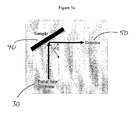
- the angle of incidence (corresponding to ⁇ ) of the pump laser 30 was varied by rotating the film sample 40 clockwise and the fluorescence was monitored at different angles of collection ⁇ by the detector 50 (see Figure 5a ).
- Lasing was observed at an angle of collection around 39° at the longer wavelength tail of the erbium gain band. Discrete modes were present in the spectrum with the longest wavelength lasing mode at 1615.15nm. The laser peaks were then systematically recorded by varying the angle at a constant incident pump power of 37.39 mW and the resulting output spectrum at different angles shown in Figure 5b .
- the observed longest wavelength spectrum corresponding to an angle of 39° is shown enlarged in Figure 6a .
- the laser emission band spanned the wavelength range of 1604.3 to 1615.15nm.
- the resolution of the spectrometer was 0.3 and peaks with widths narrower than this were not resolved.
- the peak laser wavelength was shifted towards the lower wavelengths in the gain spectrum of the erbium ions when the angle of collection was increased. Lasing with narrow spikes in the spectrum predicted in random lasers were clearly observed in the entire gain spectrum of the erbium ions and lasing was also surprisingly observed at wavelengths well below 1534nm where the absorption cross-section is greater than emission cross-section (see Figures 6b ). Lasing was observed at wavelengths as low as 1515nm (see Figure 6c ).
- Figure 10 shows the integrated laser intensity for the wavelength range 1610-1625nm plotted against incident pump power.
- the threshold of the laser is approximately 290 ⁇ W but varies at different positions on the film and for different lasing wavelengths, nevertheless the threshold is in the sub-mW range, for wavelengths above 1520 nm, and is the lowest recorded for random lasers.
- Figure 11 shows the threshold power varying with different angles of ⁇ .
- the threshold power for different values of ⁇ is tabulated in Table 1 below: Table 1: variation of threshold power with different angles of ⁇ ⁇ ° Threshold Power ( ⁇ W) 39 290 41 65 43 75 45 25 47 20 49 50 51 100
- the spot size of the laser at the film when it was oriented at a right angle to the incident laser beam was 1.36mm. That means it is lasing from an area approximately 1.45mm 2 or a volume of 1.13x10 -3 mm 3 .
- the shifting of the spectrum towards shorter wavelengths on decreasing the angle is attributed to the shortening of the photon mean free path of the photons that allow only shorter wavelengths to acquire the threshold to lase.
- the angle of collection was fixed at 48° and lasing was observed even below the threshold of the laser diode used in the experiment due to the spontaneous emission noise.
- the power was ⁇ 15 ⁇ W.
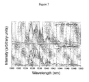
- Figure 7 shows the spectrum of the laser at two different pump powers. Excellent mode stability is evident from Figure 7 by comparing the peaks observed at two different powers well above the laser threshold. This is another characteristic of a random laser.
- the threshold power ( ⁇ 26mW/mm 2 ) is the lowest ever recorded for an erbium laser and for a random laser.
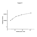
- the integrated output intensity vs incident pump power is shown in Figure 8 .
Landscapes
- Physics & Mathematics (AREA)
- Electromagnetism (AREA)
- Engineering & Computer Science (AREA)
- Plasma & Fusion (AREA)
- Optics & Photonics (AREA)
- Lasers (AREA)
- Glass Compositions (AREA)
- Optical Integrated Circuits (AREA)
Description
- The present invention relates to a method of achieving random lasing with a device which comprises a rare-earth-doped glass waveguide, to a process for fabricating the device and to a laser comprising said device.
- Lasers that rely on multiple scattering processes in a random scattering medium for optical feedback are known as random lasers. They differ from a conventional laser which relies on resonant optical feedback by reflectors or mirrors.
- Random lasing has been the subject of enormous interest to researchers in the area of solid state physics and laser physics. Initial experiments were designed to prove the principles of random lasing and not to identify an efficient laser source for applications. A disordered amplifying medium was created using a fine powder of neodymium doped crystal and random lasing was demonstrated at liquid nitrogen temperature (Markushev, V. M., Zolin, V. F. & Briskina, Ch. M., Powder laser, Zh. Prikl. Spektrosk. 45, 847-850 (1986)). Lasing was demonstrated in a liquid dye gain medium with dispersed scatterers (Martorell, J., Balachandran, R. M. & Lawandy, N. M., Radiative coupling between photonic paint layers. Opt. Lett. 21, 239-241 (1996)). In these experiments, a distinct narrowing of the emission spectrum was observed above a certain threshold which was attributed to stimulated emission in a random scattering medium leading to amplification that can be described using Letokhov's model (Letokhov, V.S. Generation of light by a scattering medium with negative resonance absorption, Zh. Eksp. Teor. Fiz. 53, 1442-1447 (1967); Sov. Phys. JETP 26, 835-840 (1968)). The discrete modes of the laser that would have been present in a random scattering medium where light can be localised was first observed by Cao and co-workers (Cao, H. et al., Random laser action in semiconductor powder, Phys. Rev. Lett. 82, 2278-2281 (1999)). The strong scattering and high gain was achieved in a ZnO nanopowder film of thickness in the range 6-10µm and coherent lasing was observed with angular dependence when pumped using a mode-locked Nd:YAG laser. The lasing threshold was 763 kW/cm2. It has been proposed that etching glass or semiconductor crystal can produce very strong scattering media for random lasing (Schuurmans, F. J. P., Vanmaekelbergh, D., van de Lagemaat, J. & Lagendijk, A., Strongly photonic macroporous GaP networks, Science 284, 141-143 (1999) and D. S. Wiersma and S. Cavalieri, "Light emission: A temperature-tunable random laser", Nature 414(6865), 708-709 (2001)).
- The media which have been used to demonstrate random lasing have been generally 3-dimensional and require a very high pump threshold to initiate lasing. The media were mostly complex, non-portable, unstable and the distribution of scatterers was non-reproducible. Modes were difficult to preserve.
- There has been interest in theoretical studies of 2D structures for random lasers (Apalkov, V. M., Raikh, M. E. & Shapiro, B., Random resonators and prelocalized modes in disordered dielectric films, Phys. Rev. Lett. 89, 016802 (2002)). The use of a random laser deploying a Tm3+ ion doped glass powder film claims to have achieved a threshold of several kilowatts per square centimetres (H. Fujiwara, and K. Sasaki, "Observation of upconversion lasing within a thulium-ion-doped glass powder film containing titanium dioxide particles", Jpn. J. Appl. Phys. 43(No. 10B), L1337-L1339 (2004)). The use of random lasers for practical applications as a coherent source has been limited because of their high threshold, low reliability and fabrication difficulties.
-
US-A-3573653 ,US-A-3579142 ,US-A-3787234 ,US-A-6574249 andUS-A-3747021 disclose thin film lasers which are pumped electrically or optically.US-A-5306385 discloses photoluminescent crystalline doped-CaF2 thin films on a silicon substrate.US-A-5783319 discloses a tunable dye laser comprising an organically doped-silica glass thin film on a silicon substrate.US-A-6656588 discloses a process for preparing a doped nanocrystalline metal oxide powder in the form of a thin film which exhibits lasing. - The present invention is based on the recognition that by confining electromagnetic radiation in a non 3-dimensional doped-glass structure it is possible to achieve improvements in random lasing. In particular, the present invention relates to a device capable of random lasing which exploits a certain rare earth-doped glass waveguide.
- Thus, viewed from one aspect the present invention provides a method for achieving random lasing using a device comprising a substrate; and a rare earth-doped glass fabricated on the substrate in the form of a waveguide, wherein the glass comprises a germanium glass, a titanium glass, or a chalcogenide glass. Said method is defined in claim 1.
- The device of the present invention is robust and reproducible and advantageously does not require Bragg or conventional mirrors making it straightforwardly integratable with other light emitting devices based on semiconductors and polymers. It exhibits excellent mode stability and is tunable over a surprisingly broad wavelength range.
- The device is optically pumpable: the device may be also electrically pumpable, but typically, the device is optically pumped.
- When the device is optically pumped, the device may begin laser emission at a certain power output from the pump laser. The minimum power required from the pump laser which causes laser emission in the device may be known as the threshold pump power. This may also be known simply as the 'threshold'. The threshold may also be expressed as a threshold pump power per unit of area of the incident area of the pump laser beam on the device (e.g., watts per mm2). This may also be known as a threshold power density. For example with a threshold pump laser power of 37mW and a pump laser beam of incident area of approximately 1.45mm2, the threshold pump power density is approximately 26mW/mm2.
- The device may be capable of random lasing at a threshold of 1mW or less to produce coherent output from an area less than 2mm2. This is equivalent to a threshold power density of 0.5mW/mm2.
- The threshold power density of the device may be less than 200mW/mm2. Preferably the threshold power density of the device is less than 100mW/mm2, particularly preferably less than 50mW/mm2, more preferably less than 26mW/mm2.
- The threshold of the device may be less than 1mW. Preferably the threshold of the device is less than 500µW, particularly preferably less than 300µW, more preferably less than 200µW, yet more preferably less than 100µW, even more preferably less than 50µW.
- The wavelength of the laser emission from the device may be dependent on the angle of incidence of the pump laser beam. The wavelength of the laser emission from the device may be tuneable. The wavelength of the laser emission from the device may be tuneable by varying the angle of incidence of the pump laser beam.
- The wavelength of the laser emission from the device may be tuneable in the range from 1510nm to 1620nm.
- The threshold pump power for the device may be dependent on the angle of incidence of the pump laser beam. The threshold pump power for the device may be tuneable by varying the angle of incidence of the pump laser beam.
- The threshold of the device may vary in the range between 300µW to 20µW as the angle of incidence of the pump laser is varied between 39° and 51°.
- Reducing the threshold or threshold power density reduces the thermal load on the device. A reduced thermal load makes the device more practically applicable because the need for heat dissipation is reduced.
- Typically the glass is non-crystalline. Typically the glass is substantially without grain boundaries.
- Preferably the glass is capable of multiple scattering. The glass is typically dielectric.
- Preferably the glass is porous, particularly preferably nanoporous. A nanoporous glass promotes multiple scattering and facilitates the fabrication of the waveguide.
- Preferably the glass is a chalcogenide glass. Particularly preferably the chalcogenide glass comprises sulphur, selenium, tellurium or a mixture thereof.
- Preferably the glass is a germanium glass or a tellurium glass, particularly preferably a tellurium glass.
- The glass may comprise (or consist essentially of) germanium dioxide (GeO2).
- GeO2 may be present in the rare earth-doped glass in an amount over 30mol%, preferably an amount in the range 60-90mol%, particularly preferably 75-85mol%.
- The glass may comprise (or consist essentially of) tellurium dioxide (TeO2). TeO2 is also known as tellurite.
- TeO2 may be present in the rare earth-doped glass in an amount over 30mol%, preferably an amount in the range 60-90mol%, particularly preferably 75-85mol%.
- The glass may further comprise one or more network modifiers. The glass may comprise four network modifiers, preferably three network modifiers, particularly preferably two network modifiers. The network modifier may open the network of the glass.
- The network modifier may be a network modifying ion. The network modifier may be a metal compound. The metal compound may provide a network modifying ion. The network modifier may be a metal fluoride or oxide. Each network modifier may be present in an amount of 30mol% or less, preferably 20mol% or less, particularly preferably 10mol% or less. Each network modifier may be present in an amount of up to 30mol%, preferably up to 20mol%, particularly preferably up to 10mol%.
- The network modifier may be an oxide of at least one of Ba, Bi, Pb, Zn, Al, Ga, La, Nb, W, Ta, Zr, Ti, V and mixtures thereof.
- Preferably the network modifier is selected from the group consisting of BaO, Bi2O3, PbO, ZnO, Ga2O3, Al2O3, La2O3, Nb2O5, WO3, Ta2O5, ZrO2, TiO2, V2O5, and mixtures thereof. The network modifier may be present in an amount of 30mol% or less, preferably 20mol% or less, particularly preferably 10mol% or less.
- Preferably the glass may further comprise one or more of MgO, CaO, SrO, BaO, ZnO, PbO, and mixtures thereof. The one or more of MgO, CaO, SrO, BaO, ZnO, PbO, and mixtures thereof may be present in an amount of 30mol% or less, preferably 20mol% or less, particularly preferably 10mol% or less. These metal oxides may also be network modifiers.
- Preferably the glass further comprises one or more alkali metal oxides. Particularly preferably the glass further comprises one or more of Li2O, Na2O and K2O, and mixtures thereof. The one or more alkali metal oxides may be present in an amount of 25mol% or less, preferably 20mol% or less, particularly preferably 10mol% or less. For example, the alkali metal oxide may be present in an amount of approximately 9mol%. The alkali metal oxide may be a network modifier.
- Preferably the glass further comprises one or more metal halides, particularly preferably an alkali metal halide. The metal halide may be a network modifier.
- The one or more metal halides may be selected from the group consisting of BaCl2, PbCl2, PbF3, LaF3, ZnF2, BaF2, NaCl, NaF, LiF, and mixtures thereof The one or more metal halides may be present in an amount of 20mol% or less.
- The glass may further comprise an alkali metal or alkaline earth metal phosphate.
- The glass may further comprise an enhancing compound comprising phosphorous or boron. The enhancing compound may be an oxide of phosphorous or boron. Preferably the enhancing compound comprises P2O5 or B2O3, or a mixture thereof. The enhancing compound may enhance the refractive index of the glass. The enhancing compound may cause random light scattering.
- The glass may be doped with a lanthanide. The glass may be doped with a lanthanide oxide.
- The glass may be doped with at least one of erbium, ytterbium, neodymium, praseodymium, holmium, cerium, yttrium, samarium, europium, gadolinium, terbium, dysprosium or lutetium.
- The glass may be doped with one or more lanthanide ions.
- Preferably the glass is doped with one or more ions selected from the group consisting of Nd3+, Yb3+, Er3+, Tm3+, Pr3+, Ho3+, Sm3+, Eu3+, Tb3+, and Ce3+.
- Preferably the glass is doped with Tm3+ or Er3+, particularly preferably Er3+.
- The rare-earth dopant is typically present in an amount in the range 0.01 to 5mol%, preferably 0.5 to 2mol% (eg, about 1mol%).
- The wavelengths at which the device is capable of random lasing may be selectable. The wavelengths may be selectable by selecting a particular rare-earth dopant or mixture of rare-earth dopants. By selecting a particular rare-earth dopant or mixture of rare-earth dopants and using an appropriate excitation/pumping scheme, the wavelengths at which the device is capable of random lasing may be selected from a range of 600nm to 5000nm.
- The glass may have an emission peak in the
range 1450 to 1650nm (eg, at about 1550nm). - The glass may have an emission cross-section greater than 1 x 10-21cm2 at a wavelength of 1535nm.
- The spectral full-width half maximum exhibited by the glass is typically 50nm or more.
- The glass may be a high refractive index glass. The glass, when in the form of a film, may have an effective refractive index of 1.5 or more. The effective refractive index at a thickness of 770nm and a wavelength of 633nm is typically about 1.55.
- The waveguide may be a fiber, channel, planar or slab waveguide. Preferred is a planar waveguide.
- The waveguide is typically in the form of a thin film. The thin film may have a thickness less than 10,000nm (10µm), preferably less that 5,000nm (5µm), preferably less than 1000nm, preferably less than 500nm. Preferably the thin film has a thickness in the range 115 to 777nm.
- The substrate may be a silicon based substrate. The substrate may be a polymeric substrate. The substrate may comprise a polymer. The substrate may comprise an electroluminescing device. The substrate may comprise a photoluminescing device.
- Preferably the substrate is a silicon-based substrate. The silicon-based substrate may be or include silicon, silica glass, silicon oxide or silicon hydride. The silicon-based substrate may be a semiconductor.
- The effective refractive index of the silicon-based substrate may be about 1.455 at 633nm.
- The device may be capable of random lasing by electrical or optical excitation. The device may be capable of random lasing by being optically excited by a 980nm continuous wave laser diode at a threshold below 50µW.
- The device may be capable of random lasing at a wavelength in the UV, visible, near-IR or mid-IR spectrum.
- The device may be obtainable by ablating a target glass with incident radiation from an ultrafast laser in the presence of a silicon-based substrate.
- Of independent patentable significance is the recognition that at certain excitation geometries, it is possible to achieve different lasing wavelengths from the device of the invention.
- Viewed from a further aspect the present invention provides a laser assembly comprising:
- a device as hereinbefore defined; and
- an exciter downstream from the device and capable of exciting the device into a laser output.
- The exciter may be a focussed exciter.
- The assembly surprisingly achieves lasing at different wavelengths across the entire spontaneous emission line width (eg, 1512.75 to 1612.15nm for erbium) without mirrors simply by varying the relative disposition of the exciter and device.
- Preferably the laser assembly is a tunable laser assembly. The tunable laser assembly may be tunable over a range of up to 100nm.
- Preferably the laser assembly further comprises a detector upstream from and capable of measuring the laser output from the device.
- Preferably the laser assembly further comprises a collector upstream from and capable of collecting the laser output from the device.
- Preferably the angular disposition of the exciter and device is adjustable. This permits the tunability of the laser assembly to be exploited.
- Preferably the exciter is a source of electromagnetic radiation. For example, the exciter may be a diode laser or light emitting diode (LED or SLED). The exciter may be a semiconductor laser. For example, the exciter may be a vertical cavity surface emitting laser (VCSEL). The exciter may be a continuous wave laser.
- The exciter may be a pump laser. The pump laser may have an output wavelength of 980nm.
- Viewed from a yet further aspect the present invention provides a process for fabricating a device as hereinbefore defined comprising:
- ablating a target glass with incident radiation from an ultrafast laser in the presence of a substrate whereby to deposit a quantity of the target glass on the substrate.
- The substrate may be a silicon based substrate. The substrate may be a polymeric substrate. The substrate may comprise a polymer. The substrate may comprise an electroluminescing device. The substrate may comprise a photoluminescing device.
- Preferably the substrate is a silicon-based substrate. The silicon-based substrate may be or include silicon, silica glass, silicon oxide or silicon hydride. The silicon-based substrate may be a semiconductor.
- Preferably the target glass is mounted on a rotational platform.
- The substrate may be spaced apart from the target glass (eg, by a distance of about 70mm). The substrate may be heated (eg, to a temperature of 600°C or more).
- The incident radiation may be incident on the target glass at an angle in the
range 40 to 80° (eg about 60°). - The ultrafast laser may be a pulsed laser. Preferably the ultrafast laser is capable of emitting ultrashort pulses which are target glass ablative. The ultrafast laser may be a femtosecond or picosecond laser. Preferably the ultrafast laser is a femtosecond laser. In the process of the invention, the ultrafast laser may emit pulses of 15ps or less (eg pulses in the range 5fs to 15ps). Preferably in the process of the invention the ultrafast laser emits pulses of 150fs or less, preferably in the
range 50 to 150fs, particularly preferably about 100fs. The pulses may be emitted with a repetition rate in the range 1 Hz to 100MHz, preferably 1kHz to 20MHz, preferably 1kHz to 1 MHz, preferably 1kHz to 200kHz. - The ultrafast laser may be mode-locked. The average power of the ultrafast laser may be 80W or less. The wavelength is typically about 800nm.
- The ultrafast laser may be (for example) a Ti-sapphire laser, a diode pumped laser such as a Yb-doped or Cr-doped crystal laser or a fibre laser.
The laser may be an excimer laser or an exciplex laser. - The pulse energy is typically in the range 1µJ to 100mJ, preferably 10µJ to 100mJ (eg in the
range 50 to 300µJ). Pulse energy may be selectively adjusted using an attenuator. - The process is typically carried out in a vacuum chamber. The process may be carried out at reduced pressure (eg, in the presence of oxygen at a partial pressure of about 70mTorr). The duration of the process may be 30 minutes or more.
- The device according to the invention may be used in communication, computer or display technology and in laser assemblies. The device according to the invention may be used in integrated optics (eg as a signal source), chemical sensing, environmental sensing, bio-sensing, micro-nano spectroscopy, optical communication, micro fluidic devices, opto-fluidic devices, terahertz amplifiers, lab-on-chip or optical tomography.
- An embodiment of the invention will now be described in detail and by way of example only with reference to the accompanying drawings in which:
-
Figure 1 shows the optical transmittance spectrum (under normal incidence) recorded using UV-VIS-NIR wavelength region of a film in a device according to an embodiment of the present invention; -
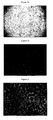
Figure 2a shows an optical micrograph of the film ofFigure 1 at a magnification of 20x; -
Figure 2b shows an optical micrograph of the film ofFigure 1 at a magnification of 50x; -
Figure 2c shows an optical micrograph of the inside of the film ofFigure 1 at a magnification of 50x; -
Figure 3 shows the fluorescence spectrum of the film in comparison to that of the glass target; -
Figure 4 shows the absorption and emission of photons by the erbium ions which provide the erbium laser mechanism; -
Figure 5a shows how the fluorescence of the film was monitored at different angles of collection θ by varying the angle of incidence of the pump laser by rotating the film clockwise; -
Figure 5b shows the resulting output spectrum at the different angular positions defined inFigure 5a ; -
Figure 6a shows the observed longest wavelength spectrum corresponding to an angle of 39° (error of ±0.5°); -
Figure 6b shows lasing was also observed at wavelengths well below 1534nm where the absorption cross-section is greater than the emission cross-section; -
Figure 6c shows that lasing was observed at wavelengths as low as 1515nm; -
Figure 7 shows the spectrum of the laser at two different pump powers; -
Figure 8 shows the integrated output intensity vs incident pump power; -
Figure 9 shows an AFM image of a section of the surface of a sample of the glass film; -
Figure 10 shows the laser emission output from a sample of the glass film; and -
Figure 11 shows the threshold power varying with different angles of θ. - A target tellurite glass was prepared by batch melting and quenching TeO2, ZnO and Na2O at a relative molar composition of 80 mol% TeO2 10mol% ZnO and 10 mol% Na2O. The glass was doped with 1 mol% erbium oxide. The resulting target tellurite glass had the composition: 80 mol% TeO2, 10 mol% ZnO, 9 mol% Na2O and 1 mol% erbium oxide. The tellurite glass has a very high refractive index (>2 at 633 nm) providing strong scattering.
- A silica glass substrate was placed at a distance of 70mm above the target tellurite glass in a chamber. The chamber was pumped down to below 10-6 Torr and oxygen atmosphere was maintained at a pressure of 70 mTorr. The substrate heater temperature was set at 700°C and held at this temperature during deposition.
- Thin films of glass were prepared by an ablation process using a femtosecond laser. The laser with a pulse duration of 100fs was focussed at an angle of incidence of 60° at the target tellurite glass. The energy of the laser with a repetition rate of 500 Hz was 52 µJ.
- Laser ablation was carried out for 3 hours. The target was rotated at a speed of 40 rpm and a proper rastering was applied to ablate the target uniformly while the substrate was at a speed of 20 rpm. The substrate was cooled down to room temperature rapidly after deposition.
- An empirical approach was deployed to optimize the process parameters to optimize the film quality. This was successful even though the relative position of the laser spot on the target with respect to the substrate was constant during the ablation. There was a thickness modulation that is attributable to the density profile of the laser plasma.
- The erbium-doped tellurite glass film fabricated on a silica glass substrate by the femtosecond laser ablation process described above was examined by different methods.
-
Figure 1 shows the optical transmittance spectrum (under normal incidence) of the film recorded using UV-VIS-NIR wavelength region. The film showed very high transmittance (> 98%) over the wavelength region and a distinct interference pattern indicative of good uniformity. - Although the results of only a single film are presented below, lasing was observed in films having lower thicknesses and different porosities. The optical properties of the film were investigated using spectroscopic ellipsometry and showed some interesting characteristics. The thickness at the middle of a sample having dimensions 3x2cm2 obtained from the ellipsometry data was 777nm and thickness variation was about 150nm/cm across the film. The thickness variation is attributed to the fact that the relative position of the laser ablation spot and the substrate was constant during deposition and the laser beam has a Gaussian intensity profile with a spot area less than 3000 µm2. The surface roughness of the film was in the range 17 to 23 nm over the surface where the lasing experiments was performed. This roughness of the film resulted in a lower effective refractive index than that of the glass target used to prepare the film. At 633nm the refractive index of the glass measured using spectroscopic ellipsometry was 1.935 whilst that of the film was 1.549 at a region where the surface roughness was 22.69nm and 1.552 at a lower roughness of 17.16nm. The results of the spectroscopic ellipsometry were a clear indication of a nanoporous film.
- The optical micrograph of the films shown in
Figure 2 revealed no cracking or peeling. However the roughness of the surface is clearly evident. In order to further understand the film morphology, atomic force microscopy (AFM) was used.Figure 9 shows an AFM image of a section of the surface of a glass film. The surface roughness of the glass film in the nanoscale can be seen clearly fromFigure 9 . The dimension of the glass strands formed on the substrate showed the random distribution. - The film was excited using a focussed beam of a fibre pigtailed laser diode with an output peaked at 980nm and the fluorescence was collected transverse to the film and detected using a liquid nitrogen cooled photomultiplier tube attached to an Edinburgh Instruments' (UK) spectrofluorimeter.
-
Figure 3 shows the fluorescence spectrum of thefilm 10 in comparison to that of the bulktellurite glass target 20. - The absorption and emission of photons by the erbium ions occurs by the process shown in
Figure 4 . The pump laser at around 980nm excites the ions to the 4I11/2 level and some ions relaxes non-radiatively to 4I13/2. The erbium ions in this excited state decay radiatively to the ground state 4I15/2 by emitting photons in the wavelength band peaked around 1535 nm. This particular emission has been exploited successfully in optical fibre and waveguide amplifiers and is the core to the success of broadband fibre optic communication systems. - The spectral width of the fluorescence signal for the film has been narrowed compared to that of the target tellurite glass. The FWHM for the glass is 72.6 nm while that of the film is only 31 nm. This narrowing of the spectrum is attributed to the amplification of spontaneous emission through scattering and stimulated emission in a random medium.
- The observed spectrum of the film is direct evidence of the model that predicts that the emission spectrum narrows down above threshold with a maximum intensity at the wavelength of maximum gain. This is manifested in the shifting of the peak of the spectrum towards longer wavelengths and also in the longer fluorescence decay lifetime of 11.9 ms observed for the film while the target was only 3.8 ms.
- Since the spectral narrowing and longer lifetime clearly pointed to random lasing with localisation, the angle of incidence (corresponding to θ) of the
pump laser 30 was varied by rotating thefilm sample 40 clockwise and the fluorescence was monitored at different angles of collection θ by the detector 50 (seeFigure 5a ). - Lasing was observed at an angle of collection around 39° at the longer wavelength tail of the erbium gain band. Discrete modes were present in the spectrum with the longest wavelength lasing mode at 1615.15nm. The laser peaks were then systematically recorded by varying the angle at a constant incident pump power of 37.39 mW and the resulting output spectrum at different angles shown in
Figure 5b . - The observed longest wavelength spectrum corresponding to an angle of 39° (error of ±0.5°) is shown enlarged in
Figure 6a . The laser emission band spanned the wavelength range of 1604.3 to 1615.15nm. The resolution of the spectrometer was 0.3 and peaks with widths narrower than this were not resolved. The peak laser wavelength was shifted towards the lower wavelengths in the gain spectrum of the erbium ions when the angle of collection was increased. Lasing with narrow spikes in the spectrum predicted in random lasers were clearly observed in the entire gain spectrum of the erbium ions and lasing was also surprisingly observed at wavelengths well below 1534nm where the absorption cross-section is greater than emission cross-section (seeFigures 6b ). Lasing was observed at wavelengths as low as 1515nm (seeFigure 6c ). -
Figure 10 shows the integrated laser intensity for the wavelength range 1610-1625nm plotted against incident pump power. The threshold of the laser is approximately 290 µW but varies at different positions on the film and for different lasing wavelengths, nevertheless the threshold is in the sub-mW range, for wavelengths above 1520 nm, and is the lowest recorded for random lasers. -
Figure 11 shows the threshold power varying with different angles of θ. The threshold power for different values of θ is tabulated in Table 1 below:Table 1: variation of threshold power with different angles of θ θ° Threshold Power (µW) 39 290 41 65 43 75 45 25 47 20 49 50 51 100 - This is a demonstration of amplification by localization, ie, a spontaneously emitted photon being amplified by the localization in a random media.
Figure 6 also shows the broad amplified spontaneous emission spectrum. This is the lowest wavelength lasing ever recorded in an erbium doped system and definitive proof of light localization in the porous glass film. - The spot size of the laser at the film when it was oriented at a right angle to the incident laser beam was 1.36mm. That means it is lasing from an area approximately 1.45mm2 or a volume of 1.13x10⁻³ mm3. The shifting of the spectrum towards shorter wavelengths on decreasing the angle is attributed to the shortening of the photon mean free path of the photons that allow only shorter wavelengths to acquire the threshold to lase.
- The angle of collection was fixed at 48° and lasing was observed even below the threshold of the laser diode used in the experiment due to the spontaneous emission noise. The power was ∼15µW.
-
Figure 7 shows the spectrum of the laser at two different pump powers. Excellent mode stability is evident fromFigure 7 by comparing the peaks observed at two different powers well above the laser threshold. This is another characteristic of a random laser. - The threshold power (<26mW/mm2) is the lowest ever recorded for an erbium laser and for a random laser. The integrated output intensity vs incident pump power is shown in
Figure 8 .
Claims (5)
- A method of achieving random lasing comprising:- fabricating a device (40) comprising a substrate and a rare earth-doped glass fabricated on the substrate in the form of a waveguide, wherein the glass comprises a germanium glass, a titanium glass or a chalcogenide glass, wherein fabricating comprises the two steps of:the method further comprises:- ablating a glass target with incident radiation from an ultrafast laser in the presence of a substrate whereby to deposit a quantity of the glass target on the substrate, and- applying rastering to ablate the glass target uniformly,- wherein the ultrafast laser emits pulses of 15ps or less and the relative position of the laser spot on the glass target with respect to the substrate is constant during the ablation and wherein the Gaussian intensity profile of the laser beam has a spot area less than 3000µm2, and- exciting the device by a source of electromagnetic radiation (30).
- A method as claimed in claim 1 wherein the ultrafast laser is a femtosecond laser.
- A method as claimed in claim 1 or 2 wherein the incident radiation from the ultrafast laser is emitted in pulses with a duration of 150fs or less.
- A method as claimed in claim 1, 2 or 3 wherein the incident radiation from the ultrafast laser is emitted in pulses with a repetition rate in the range 1 Hz to 100MHz.
- A method as claimed in any of claims 1 to 4 wherein the incident radiation pulse energy is in the range 1µJ to 100mJ.
Applications Claiming Priority (3)
| Application Number | Priority Date | Filing Date | Title |
|---|---|---|---|
| GBGB0915944.3A GB0915944D0 (en) | 2009-09-10 | 2009-09-10 | Device |
| GBGB0919472.1A GB0919472D0 (en) | 2009-09-10 | 2009-11-06 | Device |
| PCT/GB2010/051514 WO2011030157A2 (en) | 2009-09-10 | 2010-09-10 | Device |
Publications (2)
| Publication Number | Publication Date |
|---|---|
| EP2476170A2 EP2476170A2 (en) | 2012-07-18 |
| EP2476170B1 true EP2476170B1 (en) | 2015-07-08 |
Family
ID=41277551
Family Applications (1)
| Application Number | Title | Priority Date | Filing Date |
|---|---|---|---|
| EP10759700.7A Not-in-force EP2476170B1 (en) | 2009-09-10 | 2010-09-10 | Method of achieving random lasing |
Country Status (7)
| Country | Link |
|---|---|
| US (1) | US20120225220A1 (en) |
| EP (1) | EP2476170B1 (en) |
| CN (1) | CN103229371B (en) |
| ES (1) | ES2545330T3 (en) |
| GB (2) | GB0915944D0 (en) |
| SG (1) | SG179044A1 (en) |
| WO (1) | WO2011030157A2 (en) |
Families Citing this family (12)
| Publication number | Priority date | Publication date | Assignee | Title |
|---|---|---|---|---|
| EP2697858B1 (en) * | 2011-04-14 | 2019-10-23 | Yale University | Method for imaging using a random laser |
| GB201202128D0 (en) | 2012-02-08 | 2012-03-21 | Univ Leeds | Novel material |
| GB201514431D0 (en) * | 2015-08-13 | 2015-09-30 | Univ Leeds | Improvements in and relating to materials |
| EP3469423B1 (en) * | 2016-06-09 | 2020-04-15 | Osram Sylvania Inc. | Target assembly with glass-bonded wavelength converter |
| CN107749564B (en) * | 2017-11-16 | 2019-12-13 | 太原理工大学 | monolithic integrated laser chip for generating chaotic light by high-scattering doped optical waveguide feedback |
| CN107809058B (en) | 2017-11-16 | 2020-09-04 | 太原理工大学 | A monolithic integrated semiconductor random laser |
| US11784452B2 (en) * | 2019-02-25 | 2023-10-10 | Cymer, Llc | Optical element for a deep ultraviolet light source |
| CN114815442B (en) * | 2021-01-19 | 2025-06-27 | 宁波大学 | Channel type planar waveguide amplifier preparation method and channel type planar waveguide amplifier |
| CN113934079B (en) * | 2021-09-30 | 2023-04-07 | 华中科技大学 | Optical waveguide amplifier and preparation method thereof |
| CN113860750B (en) * | 2021-10-21 | 2023-03-14 | 中国计量大学 | 1-5 micron supercontinuum laser output oxyhalogen glass and preparation method thereof |
| CN114759427B (en) * | 2022-04-21 | 2025-07-18 | 江西理工大学 | Dysprosium ion activated orthophosphate mixed crystal and yellow light wave band solid laser thereof |
| CN115966987B (en) * | 2023-03-16 | 2023-06-06 | 安徽科创中光科技股份有限公司 | Multi-wavelength laser capable of being screened |
Family Cites Families (9)
| Publication number | Priority date | Publication date | Assignee | Title |
|---|---|---|---|---|
| US3747021A (en) | 1969-07-18 | 1973-07-17 | Us Navy | Wide range continuously tunable thin film laser |
| US3573653A (en) | 1969-07-18 | 1971-04-06 | Us Navy | Continuously tunable thin film laser employing the electric field effect |
| US3579142A (en) | 1969-07-18 | 1971-05-18 | Us Navy | Thin film laser |
| US3787234A (en) | 1969-07-18 | 1974-01-22 | Us Navy | Method of producing a thin film laser |
| US5306385A (en) | 1992-09-15 | 1994-04-26 | Texas Instruments Incorporated | Method for generating photoluminescence emission lines from transition element doped CAF2 thin films over a Si-based substrate |
| US5783319A (en) | 1993-11-26 | 1998-07-21 | Yissum Research Development Company Of The Hebrew University Of Jerusalem | Waveguide tunable lasers and processes for the production thereof |
| WO2000038282A2 (en) | 1998-12-01 | 2000-06-29 | The Regents Of The University Of Michigan | Ultrafine powders and their use as lasing media |
| JP2001257399A (en) | 2000-03-09 | 2001-09-21 | Taiyo Yuden Co Ltd | Thin-film laser light emitting device and method of manufacturing the same |
| KR100829064B1 (en) * | 2006-12-19 | 2008-05-19 | 연세대학교 산학협력단 | Random Raging Nanoporous Membranes with Directivity and Methods for Manufacturing the Same |
-
2009
- 2009-09-10 GB GBGB0915944.3A patent/GB0915944D0/en not_active Ceased
- 2009-11-06 GB GBGB0919472.1A patent/GB0919472D0/en not_active Ceased
-
2010
- 2010-09-10 EP EP10759700.7A patent/EP2476170B1/en not_active Not-in-force
- 2010-09-10 WO PCT/GB2010/051514 patent/WO2011030157A2/en not_active Ceased
- 2010-09-10 SG SG2012016267A patent/SG179044A1/en unknown
- 2010-09-10 CN CN201080051616.1A patent/CN103229371B/en not_active Expired - Fee Related
- 2010-09-10 US US13/395,310 patent/US20120225220A1/en not_active Abandoned
- 2010-09-10 ES ES10759700.7T patent/ES2545330T3/en active Active
Also Published As
| Publication number | Publication date |
|---|---|
| WO2011030157A3 (en) | 2011-05-05 |
| ES2545330T3 (en) | 2015-09-10 |
| EP2476170A2 (en) | 2012-07-18 |
| CN103229371A (en) | 2013-07-31 |
| CN103229371B (en) | 2016-05-04 |
| SG179044A1 (en) | 2012-04-27 |
| WO2011030157A2 (en) | 2011-03-17 |
| GB0915944D0 (en) | 2009-10-28 |
| US20120225220A1 (en) | 2012-09-06 |
| GB0919472D0 (en) | 2009-12-23 |
Similar Documents
| Publication | Publication Date | Title |
|---|---|---|
| CN103229371B (en) | device | |
| Loiko et al. | Efficient Tm: LiYF 4 Lasers at ${\sim} 2.3~\mu $ m: Effect of Energy-Transfer Upconversion | |
| Huber et al. | Solid-state lasers: status and future | |
| US20150132507A1 (en) | Medium For Random Laser And Manufacturing Process of the Same | |
| Smart et al. | CW room temperature operation of praseodymium-doped fluorozirconate glass fibre lasers in the blue-green, green and red spectral regions | |
| Loiko et al. | Vibronic thulium laser at 2131 nm Q-switched by single-walled carbon nanotubes | |
| Chen et al. | Fluorite-type Tm3+: KY3F10: A promising crystal for watt-level lasers at∼ 1.9 μm | |
| Gaponenko et al. | Compact passively Q-switched diode-pumped Tm: KY (WO4) 2 laser with 8 ns/30 μJ pulses | |
| Tang et al. | High power Ho: YAP laser with 107 W of output power at 2117 nm | |
| Lakshminarayana et al. | Spectral analysis of RE3+ (RE= Er, Nd, Pr and Ho): GeO2–B2O3–ZnO–LiF glasses | |
| Xiong et al. | Femtosecond laser direct writing of compact Tm: YLF waveguide lasers | |
| Chen et al. | Spectra and diode-pumped continuous-wave 1.55 µm laser of Er: Yb: Ca3NbGa3Si2O14 crystal | |
| Selivanov et al. | Nonlinear refractive properties of Yb3+-doped KY (WO4) 2 and YVO4 laser crystals | |
| Ryabochkina et al. | Structural, spectral-luminescent, and lasing properties of nanostructured Tm: CaF2 ceramics | |
| Rudenkov et al. | High power SESAM mode-locked laser based on Yb3+: YAlO3 bulk crystal | |
| Mandrik et al. | CW and Q-switched diode-pumped laser operation of Yb3+: NaLa (MoO4) 2 | |
| Schlaghecken et al. | Pulsed laser deposition of Er: BaTiO3 for planar waveguides | |
| Cerdán et al. | Waveguides and quasi-waveguides based on pyrromethene 597-doped poly (methyl methacrylate) | |
| Cankaya et al. | Bulk Nd3+-doped tellurite glass laser at 1.37 μm | |
| Dubinskii et al. | Processing technology, laser, optical and thermal properties of ceramic laser gain materials | |
| Gottmann et al. | Manufacturing of Er: ZBLAN ridge waveguides by pulsed laser deposition and ultrafast laser micromachining for green integrated lasers | |
| Jenouvrier et al. | Influence of crystallisation on the photoluminescence properties of Y2-xErxTi2O7 sol-gel thin films | |
| Kurilchik et al. | Characterisation and laser performance of a Yb: LuAG double-clad planar waveguide grown by pulsed laser deposition | |
| Kuzminykh et al. | Nd3+ doped Sc2O3 waveguiding film produced by pulsed laser deposition | |
| Yang et al. | Diode-pumped continuous wave operation and passively Q-switched performances of a Nd: Sc2SiO5 laser crystal at 1.08 microns |
Legal Events
| Date | Code | Title | Description |
|---|---|---|---|
| PUAI | Public reference made under article 153(3) epc to a published international application that has entered the european phase |
Free format text: ORIGINAL CODE: 0009012 |
|
| 17P | Request for examination filed |
Effective date: 20120312 |
|
| AK | Designated contracting states |
Kind code of ref document: A2 Designated state(s): AL AT BE BG CH CY CZ DE DK EE ES FI FR GB GR HR HU IE IS IT LI LT LU LV MC MK MT NL NO PL PT RO SE SI SK SM TR |
|
| DAX | Request for extension of the european patent (deleted) | ||
| 17Q | First examination report despatched |
Effective date: 20130507 |
|
| RIC1 | Information provided on ipc code assigned before grant |
Ipc: H01S 3/063 20060101AFI20140910BHEP Ipc: H01S 3/16 20060101ALN20140910BHEP Ipc: H01S 3/23 20060101ALI20140910BHEP Ipc: H01S 3/0941 20060101ALN20140910BHEP Ipc: H01S 3/17 20060101ALN20140910BHEP |
|
| REG | Reference to a national code |
Ref country code: DE Ref legal event code: R079 Ref document number: 602010025761 Country of ref document: DE Free format text: PREVIOUS MAIN CLASS: H01S0003300000 Ipc: H01S0003063000 |
|
| GRAP | Despatch of communication of intention to grant a patent |
Free format text: ORIGINAL CODE: EPIDOSNIGR1 |
|
| RIC1 | Information provided on ipc code assigned before grant |
Ipc: H01S 3/16 20060101ALN20150113BHEP Ipc: H01S 3/0941 20060101ALN20150113BHEP Ipc: H01S 3/23 20060101ALI20150113BHEP Ipc: H01S 3/063 20060101AFI20150113BHEP Ipc: H01S 3/17 20060101ALN20150113BHEP |
|
| INTG | Intention to grant announced |
Effective date: 20150130 |
|
| RIN1 | Information on inventor provided before grant (corrected) |
Inventor name: JHA, ANIMESH Inventor name: JOSE, GIN Inventor name: STEENSON, DAVID PAUL |
|
| GRAS | Grant fee paid |
Free format text: ORIGINAL CODE: EPIDOSNIGR3 |
|
| GRAA | (expected) grant |
Free format text: ORIGINAL CODE: 0009210 |
|
| AK | Designated contracting states |
Kind code of ref document: B1 Designated state(s): AL AT BE BG CH CY CZ DE DK EE ES FI FR GB GR HR HU IE IS IT LI LT LU LV MC MK MT NL NO PL PT RO SE SI SK SM TR |
|
| REG | Reference to a national code |
Ref country code: GB Ref legal event code: FG4D |
|
| REG | Reference to a national code |
Ref country code: AT Ref legal event code: REF Ref document number: 736043 Country of ref document: AT Kind code of ref document: T Effective date: 20150715 Ref country code: CH Ref legal event code: NV Representative=s name: RIEDERER HASLER AND PARTNER PATENTANWAELTE AG, LI Ref country code: CH Ref legal event code: EP |
|
| REG | Reference to a national code |
Ref country code: IE Ref legal event code: FG4D |
|
| REG | Reference to a national code |
Ref country code: DE Ref legal event code: R096 Ref document number: 602010025761 Country of ref document: DE |
|
| REG | Reference to a national code |
Ref country code: ES Ref legal event code: FG2A Ref document number: 2545330 Country of ref document: ES Kind code of ref document: T3 Effective date: 20150910 |
|
| REG | Reference to a national code |
Ref country code: AT Ref legal event code: MK05 Ref document number: 736043 Country of ref document: AT Kind code of ref document: T Effective date: 20150708 |
|
| REG | Reference to a national code |
Ref country code: NL Ref legal event code: FP |
|
| REG | Reference to a national code |
Ref country code: LT Ref legal event code: MG4D |
|
| PG25 | Lapsed in a contracting state [announced via postgrant information from national office to epo] |
Ref country code: GR Free format text: LAPSE BECAUSE OF FAILURE TO SUBMIT A TRANSLATION OF THE DESCRIPTION OR TO PAY THE FEE WITHIN THE PRESCRIBED TIME-LIMIT Effective date: 20151009 Ref country code: NO Free format text: LAPSE BECAUSE OF FAILURE TO SUBMIT A TRANSLATION OF THE DESCRIPTION OR TO PAY THE FEE WITHIN THE PRESCRIBED TIME-LIMIT Effective date: 20151008 Ref country code: LT Free format text: LAPSE BECAUSE OF FAILURE TO SUBMIT A TRANSLATION OF THE DESCRIPTION OR TO PAY THE FEE WITHIN THE PRESCRIBED TIME-LIMIT Effective date: 20150708 Ref country code: LV Free format text: LAPSE BECAUSE OF FAILURE TO SUBMIT A TRANSLATION OF THE DESCRIPTION OR TO PAY THE FEE WITHIN THE PRESCRIBED TIME-LIMIT Effective date: 20150708 Ref country code: FI Free format text: LAPSE BECAUSE OF FAILURE TO SUBMIT A TRANSLATION OF THE DESCRIPTION OR TO PAY THE FEE WITHIN THE PRESCRIBED TIME-LIMIT Effective date: 20150708 |
|
| PG25 | Lapsed in a contracting state [announced via postgrant information from national office to epo] |
Ref country code: PL Free format text: LAPSE BECAUSE OF FAILURE TO SUBMIT A TRANSLATION OF THE DESCRIPTION OR TO PAY THE FEE WITHIN THE PRESCRIBED TIME-LIMIT Effective date: 20150708 Ref country code: HR Free format text: LAPSE BECAUSE OF FAILURE TO SUBMIT A TRANSLATION OF THE DESCRIPTION OR TO PAY THE FEE WITHIN THE PRESCRIBED TIME-LIMIT Effective date: 20150708 Ref country code: SE Free format text: LAPSE BECAUSE OF FAILURE TO SUBMIT A TRANSLATION OF THE DESCRIPTION OR TO PAY THE FEE WITHIN THE PRESCRIBED TIME-LIMIT Effective date: 20150708 Ref country code: AT Free format text: LAPSE BECAUSE OF FAILURE TO SUBMIT A TRANSLATION OF THE DESCRIPTION OR TO PAY THE FEE WITHIN THE PRESCRIBED TIME-LIMIT Effective date: 20150708 Ref country code: IS Free format text: LAPSE BECAUSE OF FAILURE TO SUBMIT A TRANSLATION OF THE DESCRIPTION OR TO PAY THE FEE WITHIN THE PRESCRIBED TIME-LIMIT Effective date: 20151108 Ref country code: PT Free format text: LAPSE BECAUSE OF FAILURE TO SUBMIT A TRANSLATION OF THE DESCRIPTION OR TO PAY THE FEE WITHIN THE PRESCRIBED TIME-LIMIT Effective date: 20151109 |
|
| REG | Reference to a national code |
Ref country code: DE Ref legal event code: R097 Ref document number: 602010025761 Country of ref document: DE |
|
| PG25 | Lapsed in a contracting state [announced via postgrant information from national office to epo] |
Ref country code: SK Free format text: LAPSE BECAUSE OF FAILURE TO SUBMIT A TRANSLATION OF THE DESCRIPTION OR TO PAY THE FEE WITHIN THE PRESCRIBED TIME-LIMIT Effective date: 20150708 Ref country code: DK Free format text: LAPSE BECAUSE OF FAILURE TO SUBMIT A TRANSLATION OF THE DESCRIPTION OR TO PAY THE FEE WITHIN THE PRESCRIBED TIME-LIMIT Effective date: 20150708 Ref country code: CZ Free format text: LAPSE BECAUSE OF FAILURE TO SUBMIT A TRANSLATION OF THE DESCRIPTION OR TO PAY THE FEE WITHIN THE PRESCRIBED TIME-LIMIT Effective date: 20150708 Ref country code: EE Free format text: LAPSE BECAUSE OF FAILURE TO SUBMIT A TRANSLATION OF THE DESCRIPTION OR TO PAY THE FEE WITHIN THE PRESCRIBED TIME-LIMIT Effective date: 20150708 Ref country code: LU Free format text: LAPSE BECAUSE OF FAILURE TO SUBMIT A TRANSLATION OF THE DESCRIPTION OR TO PAY THE FEE WITHIN THE PRESCRIBED TIME-LIMIT Effective date: 20150910 Ref country code: MC Free format text: LAPSE BECAUSE OF FAILURE TO SUBMIT A TRANSLATION OF THE DESCRIPTION OR TO PAY THE FEE WITHIN THE PRESCRIBED TIME-LIMIT Effective date: 20150708 |
|
| PLBE | No opposition filed within time limit |
Free format text: ORIGINAL CODE: 0009261 |
|
| STAA | Information on the status of an ep patent application or granted ep patent |
Free format text: STATUS: NO OPPOSITION FILED WITHIN TIME LIMIT |
|
| PG25 | Lapsed in a contracting state [announced via postgrant information from national office to epo] |
Ref country code: RO Free format text: LAPSE BECAUSE OF FAILURE TO SUBMIT A TRANSLATION OF THE DESCRIPTION OR TO PAY THE FEE WITHIN THE PRESCRIBED TIME-LIMIT Effective date: 20150708 |
|
| 26N | No opposition filed |
Effective date: 20160411 |
|
| PG25 | Lapsed in a contracting state [announced via postgrant information from national office to epo] |
Ref country code: SI Free format text: LAPSE BECAUSE OF FAILURE TO SUBMIT A TRANSLATION OF THE DESCRIPTION OR TO PAY THE FEE WITHIN THE PRESCRIBED TIME-LIMIT Effective date: 20150708 |
|
| REG | Reference to a national code |
Ref country code: FR Ref legal event code: PLFP Year of fee payment: 7 |
|
| PG25 | Lapsed in a contracting state [announced via postgrant information from national office to epo] |
Ref country code: BE Free format text: LAPSE BECAUSE OF FAILURE TO SUBMIT A TRANSLATION OF THE DESCRIPTION OR TO PAY THE FEE WITHIN THE PRESCRIBED TIME-LIMIT Effective date: 20150708 |
|
| PG25 | Lapsed in a contracting state [announced via postgrant information from national office to epo] |
Ref country code: MT Free format text: LAPSE BECAUSE OF FAILURE TO SUBMIT A TRANSLATION OF THE DESCRIPTION OR TO PAY THE FEE WITHIN THE PRESCRIBED TIME-LIMIT Effective date: 20150708 |
|
| PG25 | Lapsed in a contracting state [announced via postgrant information from national office to epo] |
Ref country code: HU Free format text: LAPSE BECAUSE OF FAILURE TO SUBMIT A TRANSLATION OF THE DESCRIPTION OR TO PAY THE FEE WITHIN THE PRESCRIBED TIME-LIMIT; INVALID AB INITIO Effective date: 20100910 Ref country code: BG Free format text: LAPSE BECAUSE OF FAILURE TO SUBMIT A TRANSLATION OF THE DESCRIPTION OR TO PAY THE FEE WITHIN THE PRESCRIBED TIME-LIMIT Effective date: 20150708 Ref country code: SM Free format text: LAPSE BECAUSE OF FAILURE TO SUBMIT A TRANSLATION OF THE DESCRIPTION OR TO PAY THE FEE WITHIN THE PRESCRIBED TIME-LIMIT Effective date: 20150708 |
|
| PG25 | Lapsed in a contracting state [announced via postgrant information from national office to epo] |
Ref country code: CY Free format text: LAPSE BECAUSE OF FAILURE TO SUBMIT A TRANSLATION OF THE DESCRIPTION OR TO PAY THE FEE WITHIN THE PRESCRIBED TIME-LIMIT Effective date: 20150708 |
|
| PG25 | Lapsed in a contracting state [announced via postgrant information from national office to epo] |
Ref country code: TR Free format text: LAPSE BECAUSE OF FAILURE TO SUBMIT A TRANSLATION OF THE DESCRIPTION OR TO PAY THE FEE WITHIN THE PRESCRIBED TIME-LIMIT Effective date: 20150708 |
|
| REG | Reference to a national code |
Ref country code: FR Ref legal event code: PLFP Year of fee payment: 8 |
|
| PG25 | Lapsed in a contracting state [announced via postgrant information from national office to epo] |
Ref country code: MK Free format text: LAPSE BECAUSE OF FAILURE TO SUBMIT A TRANSLATION OF THE DESCRIPTION OR TO PAY THE FEE WITHIN THE PRESCRIBED TIME-LIMIT Effective date: 20150708 |
|
| REG | Reference to a national code |
Ref country code: FR Ref legal event code: PLFP Year of fee payment: 9 |
|
| PG25 | Lapsed in a contracting state [announced via postgrant information from national office to epo] |
Ref country code: AL Free format text: LAPSE BECAUSE OF FAILURE TO SUBMIT A TRANSLATION OF THE DESCRIPTION OR TO PAY THE FEE WITHIN THE PRESCRIBED TIME-LIMIT Effective date: 20150708 |
|
| PGFP | Annual fee paid to national office [announced via postgrant information from national office to epo] |
Ref country code: FR Payment date: 20190927 Year of fee payment: 10 Ref country code: IE Payment date: 20190923 Year of fee payment: 10 Ref country code: IT Payment date: 20190925 Year of fee payment: 10 Ref country code: DE Payment date: 20190918 Year of fee payment: 10 Ref country code: NL Payment date: 20190918 Year of fee payment: 10 |
|
| PGFP | Annual fee paid to national office [announced via postgrant information from national office to epo] |
Ref country code: GB Payment date: 20190823 Year of fee payment: 10 |
|
| PGFP | Annual fee paid to national office [announced via postgrant information from national office to epo] |
Ref country code: CH Payment date: 20190919 Year of fee payment: 10 |
|
| PGFP | Annual fee paid to national office [announced via postgrant information from national office to epo] |
Ref country code: ES Payment date: 20191022 Year of fee payment: 10 |
|
| REG | Reference to a national code |
Ref country code: DE Ref legal event code: R119 Ref document number: 602010025761 Country of ref document: DE |
|
| REG | Reference to a national code |
Ref country code: CH Ref legal event code: PL |
|
| REG | Reference to a national code |
Ref country code: NL Ref legal event code: MM Effective date: 20201001 |
|
| GBPC | Gb: european patent ceased through non-payment of renewal fee |
Effective date: 20200910 |
|
| PG25 | Lapsed in a contracting state [announced via postgrant information from national office to epo] |
Ref country code: NL Free format text: LAPSE BECAUSE OF NON-PAYMENT OF DUE FEES Effective date: 20201001 |
|
| PG25 | Lapsed in a contracting state [announced via postgrant information from national office to epo] |
Ref country code: DE Free format text: LAPSE BECAUSE OF NON-PAYMENT OF DUE FEES Effective date: 20210401 Ref country code: FR Free format text: LAPSE BECAUSE OF NON-PAYMENT OF DUE FEES Effective date: 20200930 |
|
| PG25 | Lapsed in a contracting state [announced via postgrant information from national office to epo] |
Ref country code: CH Free format text: LAPSE BECAUSE OF NON-PAYMENT OF DUE FEES Effective date: 20200930 Ref country code: LI Free format text: LAPSE BECAUSE OF NON-PAYMENT OF DUE FEES Effective date: 20200930 Ref country code: GB Free format text: LAPSE BECAUSE OF NON-PAYMENT OF DUE FEES Effective date: 20200910 Ref country code: IE Free format text: LAPSE BECAUSE OF NON-PAYMENT OF DUE FEES Effective date: 20200910 |
|
| PG25 | Lapsed in a contracting state [announced via postgrant information from national office to epo] |
Ref country code: IT Free format text: LAPSE BECAUSE OF NON-PAYMENT OF DUE FEES Effective date: 20200910 |
|
| REG | Reference to a national code |
Ref country code: ES Ref legal event code: FD2A Effective date: 20220117 |
|
| PG25 | Lapsed in a contracting state [announced via postgrant information from national office to epo] |
Ref country code: ES Free format text: LAPSE BECAUSE OF NON-PAYMENT OF DUE FEES Effective date: 20200911 |