EP2472622A2 - Liquid ejecting head, liquid ejecting device and piezoelectric element - Google Patents
Liquid ejecting head, liquid ejecting device and piezoelectric element Download PDFInfo
- Publication number
- EP2472622A2 EP2472622A2 EP11195574A EP11195574A EP2472622A2 EP 2472622 A2 EP2472622 A2 EP 2472622A2 EP 11195574 A EP11195574 A EP 11195574A EP 11195574 A EP11195574 A EP 11195574A EP 2472622 A2 EP2472622 A2 EP 2472622A2
- Authority
- EP
- European Patent Office
- Prior art keywords
- piezoelectric
- site
- piezoelectric element
- liquid ejecting
- addition
- Prior art date
- Legal status (The legal status is an assumption and is not a legal conclusion. Google has not performed a legal analysis and makes no representation as to the accuracy of the status listed.)
- Withdrawn
Links
Images








Classifications
-
- B—PERFORMING OPERATIONS; TRANSPORTING
- B41—PRINTING; LINING MACHINES; TYPEWRITERS; STAMPS
- B41J—TYPEWRITERS; SELECTIVE PRINTING MECHANISMS, i.e. MECHANISMS PRINTING OTHERWISE THAN FROM A FORME; CORRECTION OF TYPOGRAPHICAL ERRORS
- B41J2/00—Typewriters or selective printing mechanisms characterised by the printing or marking process for which they are designed
- B41J2/005—Typewriters or selective printing mechanisms characterised by the printing or marking process for which they are designed characterised by bringing liquid or particles selectively into contact with a printing material
- B41J2/01—Ink jet
- B41J2/135—Nozzles
- B41J2/14—Structure thereof only for on-demand ink jet heads
- B41J2/14201—Structure of print heads with piezoelectric elements
- B41J2/14233—Structure of print heads with piezoelectric elements of film type, deformed by bending and disposed on a diaphragm
-
- B—PERFORMING OPERATIONS; TRANSPORTING
- B41—PRINTING; LINING MACHINES; TYPEWRITERS; STAMPS
- B41J—TYPEWRITERS; SELECTIVE PRINTING MECHANISMS, i.e. MECHANISMS PRINTING OTHERWISE THAN FROM A FORME; CORRECTION OF TYPOGRAPHICAL ERRORS
- B41J2/00—Typewriters or selective printing mechanisms characterised by the printing or marking process for which they are designed
- B41J2/005—Typewriters or selective printing mechanisms characterised by the printing or marking process for which they are designed characterised by bringing liquid or particles selectively into contact with a printing material
- B41J2/01—Ink jet
- B41J2/135—Nozzles
- B41J2/16—Production of nozzles
- B41J2/1607—Production of print heads with piezoelectric elements
- B41J2/161—Production of print heads with piezoelectric elements of film type, deformed by bending and disposed on a diaphragm
-
- B—PERFORMING OPERATIONS; TRANSPORTING
- B41—PRINTING; LINING MACHINES; TYPEWRITERS; STAMPS
- B41J—TYPEWRITERS; SELECTIVE PRINTING MECHANISMS, i.e. MECHANISMS PRINTING OTHERWISE THAN FROM A FORME; CORRECTION OF TYPOGRAPHICAL ERRORS
- B41J2/00—Typewriters or selective printing mechanisms characterised by the printing or marking process for which they are designed
- B41J2/005—Typewriters or selective printing mechanisms characterised by the printing or marking process for which they are designed characterised by bringing liquid or particles selectively into contact with a printing material
- B41J2/01—Ink jet
- B41J2/135—Nozzles
- B41J2/16—Production of nozzles
- B41J2/1621—Manufacturing processes
- B41J2/1623—Manufacturing processes bonding and adhesion
-
- B—PERFORMING OPERATIONS; TRANSPORTING
- B41—PRINTING; LINING MACHINES; TYPEWRITERS; STAMPS
- B41J—TYPEWRITERS; SELECTIVE PRINTING MECHANISMS, i.e. MECHANISMS PRINTING OTHERWISE THAN FROM A FORME; CORRECTION OF TYPOGRAPHICAL ERRORS
- B41J2/00—Typewriters or selective printing mechanisms characterised by the printing or marking process for which they are designed
- B41J2/005—Typewriters or selective printing mechanisms characterised by the printing or marking process for which they are designed characterised by bringing liquid or particles selectively into contact with a printing material
- B41J2/01—Ink jet
- B41J2/135—Nozzles
- B41J2/16—Production of nozzles
- B41J2/1621—Manufacturing processes
- B41J2/1626—Manufacturing processes etching
- B41J2/1628—Manufacturing processes etching dry etching
-
- B—PERFORMING OPERATIONS; TRANSPORTING
- B41—PRINTING; LINING MACHINES; TYPEWRITERS; STAMPS
- B41J—TYPEWRITERS; SELECTIVE PRINTING MECHANISMS, i.e. MECHANISMS PRINTING OTHERWISE THAN FROM A FORME; CORRECTION OF TYPOGRAPHICAL ERRORS
- B41J2/00—Typewriters or selective printing mechanisms characterised by the printing or marking process for which they are designed
- B41J2/005—Typewriters or selective printing mechanisms characterised by the printing or marking process for which they are designed characterised by bringing liquid or particles selectively into contact with a printing material
- B41J2/01—Ink jet
- B41J2/135—Nozzles
- B41J2/16—Production of nozzles
- B41J2/1621—Manufacturing processes
- B41J2/1626—Manufacturing processes etching
- B41J2/1629—Manufacturing processes etching wet etching
-
- B—PERFORMING OPERATIONS; TRANSPORTING
- B41—PRINTING; LINING MACHINES; TYPEWRITERS; STAMPS
- B41J—TYPEWRITERS; SELECTIVE PRINTING MECHANISMS, i.e. MECHANISMS PRINTING OTHERWISE THAN FROM A FORME; CORRECTION OF TYPOGRAPHICAL ERRORS
- B41J2/00—Typewriters or selective printing mechanisms characterised by the printing or marking process for which they are designed
- B41J2/005—Typewriters or selective printing mechanisms characterised by the printing or marking process for which they are designed characterised by bringing liquid or particles selectively into contact with a printing material
- B41J2/01—Ink jet
- B41J2/135—Nozzles
- B41J2/16—Production of nozzles
- B41J2/1621—Manufacturing processes
- B41J2/164—Manufacturing processes thin film formation
- B41J2/1645—Manufacturing processes thin film formation thin film formation by spincoating
-
- B—PERFORMING OPERATIONS; TRANSPORTING
- B41—PRINTING; LINING MACHINES; TYPEWRITERS; STAMPS
- B41J—TYPEWRITERS; SELECTIVE PRINTING MECHANISMS, i.e. MECHANISMS PRINTING OTHERWISE THAN FROM A FORME; CORRECTION OF TYPOGRAPHICAL ERRORS
- B41J2/00—Typewriters or selective printing mechanisms characterised by the printing or marking process for which they are designed
- B41J2/005—Typewriters or selective printing mechanisms characterised by the printing or marking process for which they are designed characterised by bringing liquid or particles selectively into contact with a printing material
- B41J2/01—Ink jet
- B41J2/135—Nozzles
- B41J2/16—Production of nozzles
- B41J2/1621—Manufacturing processes
- B41J2/164—Manufacturing processes thin film formation
- B41J2/1646—Manufacturing processes thin film formation thin film formation by sputtering
-
- H—ELECTRICITY
- H10—SEMICONDUCTOR DEVICES; ELECTRIC SOLID-STATE DEVICES NOT OTHERWISE PROVIDED FOR
- H10N—ELECTRIC SOLID-STATE DEVICES NOT OTHERWISE PROVIDED FOR
- H10N30/00—Piezoelectric or electrostrictive devices
- H10N30/01—Manufacture or treatment
- H10N30/07—Forming of piezoelectric or electrostrictive parts or bodies on an electrical element or another base
- H10N30/074—Forming of piezoelectric or electrostrictive parts or bodies on an electrical element or another base by depositing piezoelectric or electrostrictive layers, e.g. aerosol or screen printing
- H10N30/077—Forming of piezoelectric or electrostrictive parts or bodies on an electrical element or another base by depositing piezoelectric or electrostrictive layers, e.g. aerosol or screen printing by liquid phase deposition
- H10N30/078—Forming of piezoelectric or electrostrictive parts or bodies on an electrical element or another base by depositing piezoelectric or electrostrictive layers, e.g. aerosol or screen printing by liquid phase deposition by sol-gel deposition
-
- H—ELECTRICITY
- H10—SEMICONDUCTOR DEVICES; ELECTRIC SOLID-STATE DEVICES NOT OTHERWISE PROVIDED FOR
- H10N—ELECTRIC SOLID-STATE DEVICES NOT OTHERWISE PROVIDED FOR
- H10N30/00—Piezoelectric or electrostrictive devices
- H10N30/704—Piezoelectric or electrostrictive devices based on piezoelectric or electrostrictive films or coatings
-
- H—ELECTRICITY
- H10—SEMICONDUCTOR DEVICES; ELECTRIC SOLID-STATE DEVICES NOT OTHERWISE PROVIDED FOR
- H10N—ELECTRIC SOLID-STATE DEVICES NOT OTHERWISE PROVIDED FOR
- H10N30/00—Piezoelectric or electrostrictive devices
- H10N30/80—Constructional details
- H10N30/85—Piezoelectric or electrostrictive active materials
- H10N30/853—Ceramic compositions
- H10N30/8561—Bismuth-based oxides
-
- B—PERFORMING OPERATIONS; TRANSPORTING
- B41—PRINTING; LINING MACHINES; TYPEWRITERS; STAMPS
- B41J—TYPEWRITERS; SELECTIVE PRINTING MECHANISMS, i.e. MECHANISMS PRINTING OTHERWISE THAN FROM A FORME; CORRECTION OF TYPOGRAPHICAL ERRORS
- B41J2/00—Typewriters or selective printing mechanisms characterised by the printing or marking process for which they are designed
- B41J2/005—Typewriters or selective printing mechanisms characterised by the printing or marking process for which they are designed characterised by bringing liquid or particles selectively into contact with a printing material
- B41J2/01—Ink jet
- B41J2/135—Nozzles
- B41J2/14—Structure thereof only for on-demand ink jet heads
- B41J2/14201—Structure of print heads with piezoelectric elements
- B41J2/14233—Structure of print heads with piezoelectric elements of film type, deformed by bending and disposed on a diaphragm
- B41J2002/14241—Structure of print heads with piezoelectric elements of film type, deformed by bending and disposed on a diaphragm having a cover around the piezoelectric thin film element
-
- B—PERFORMING OPERATIONS; TRANSPORTING
- B41—PRINTING; LINING MACHINES; TYPEWRITERS; STAMPS
- B41J—TYPEWRITERS; SELECTIVE PRINTING MECHANISMS, i.e. MECHANISMS PRINTING OTHERWISE THAN FROM A FORME; CORRECTION OF TYPOGRAPHICAL ERRORS
- B41J2/00—Typewriters or selective printing mechanisms characterised by the printing or marking process for which they are designed
- B41J2/005—Typewriters or selective printing mechanisms characterised by the printing or marking process for which they are designed characterised by bringing liquid or particles selectively into contact with a printing material
- B41J2/01—Ink jet
- B41J2/135—Nozzles
- B41J2/14—Structure thereof only for on-demand ink jet heads
- B41J2002/14419—Manifold
-
- B—PERFORMING OPERATIONS; TRANSPORTING
- B41—PRINTING; LINING MACHINES; TYPEWRITERS; STAMPS
- B41J—TYPEWRITERS; SELECTIVE PRINTING MECHANISMS, i.e. MECHANISMS PRINTING OTHERWISE THAN FROM A FORME; CORRECTION OF TYPOGRAPHICAL ERRORS
- B41J2202/00—Embodiments of or processes related to ink-jet or thermal heads
- B41J2202/01—Embodiments of or processes related to ink-jet heads
- B41J2202/03—Specific materials used
Definitions
- the present invention relates to a piezoelectric element and a liquid ejecting head and liquid ejecting device.
- the piezoelectric element can cause a pressure change in a pressure generating chamber communicating with a nozzle opening and having a piezoelectric layer and an electrode that applies a voltage to the piezoelectric layer.
- a piezoelectric actuator for a liquid ejecting head may use a piezoelectric element configured by interposing a piezoelectric layer made of piezoelectric material showing an electromechanical transduction function, for example, crystallized dielectric material, between two electrodes.
- a piezoelectric element configured by interposing a piezoelectric layer made of piezoelectric material showing an electromechanical transduction function, for example, crystallized dielectric material, between two electrodes.
- the liquid ejecting head there is an ink jet recording head in which a pressure generating chamber communicating with a nozzle opening discharging ink droplets is partially configured as a vibration plate so that the ink in the pressure generating chamber is pressed by transforming the vibration plate by the piezoelectric element to be discharged as ink droplets from the nozzle opening.
- the piezoelectric material used for the piezoelectric layer (piezoelectric ceramics) of the piezoelectric element requires high piezoelectric features, as a representative example of such lead zirconate titanate (PZT) is given ( JP-A-2001-223404 ).
- a piezoelectric material not containing lead there is BiFeO 3 having a Perovskite-type structure expressed by ABO 3 .
- a and B of ABO 3 represent an A site and a B site, which are respectively sites where oxygen is 12-coordinated and 6-coordinated.
- the BiFeO 3 -based piezoelectric material has low insulation and tends to cause a leakage current. If a leakage current tends to occur, particularly when a high voltage is applied, cracks may be generated, and so the material is not useful for the liquid ejecting head.
- a piezoelectric material may have high insulation of 1 ⁇ 10 -3 A/cm 2 or less when a representative driving voltage of 25 V is applied.
- this problem is present not only in the ink jet recording head but also in other liquid ejecting heads which discharge liquid droplets other than ink and the piezoelectric element used for equipment other than the liquid ejecting heads.
- the leakage current problem causes a serious problem of an increase in energy consumption when the piezoelectric element is used as a sensor.
- a low leakage current is desirable even for piezoelectric elements used for piezoelectric sensors, infrared sensors, temperature sensors and pyroelectric sensors to which a voltage of 1 V or less is applied.
- An advantage of some aspects of the invention is that it provides a piezoelectric element, a liquid ejecting head, and a liquid ejecting device which are environmentally friendly, and wherein the piezoelectric element has high insulation so that leakage current is suppressed.
- a piezoelectric element which includes a piezoelectric layer and an electrode in connection with the piezoelectric layer, wherein the piezoelectric layer is made of complex oxide having a Perovskite-type structure ABO 3 (wherein A is a 12-coordinated metal site, B is a 6-coordinated metal site and O is an oxygen site) containing bismuth and iron and wherein nitrogen is included at some oxygen sites.
- the piezoelectric element has high insulation so that leakage current is suppressed, resulting in great durability.
- the burden on the environment may decrease.
- nitrogen is included in an amount of 0.0005 to 0.01 moles per mole of the Perovskite-type complex oxide.
- bismuth is partially included at the B site.
- the complex oxide further comprises titanium and barium in addition to bismuth and iron.
- the piezoelectric element has further superior piezoelectric characteristics (amount of deformation) .
- a liquid ejectring head which includes a pressure generating chamber communicating with a nozzle opening; and the above-defined piezoelectric element.
- the piezoelectric element since the piezoelectric element has high insulation due to the suppression of leakage current, it is possible to implement a liquid ejecting device with excellent durability. In addition, since lead is not contained, the burden on the environment may decrease.
- a liquid ejecting device including the liquid ejecting head of the above aspect.
- Fig. 1 is an exploded perspective view showing a schematic configuration of a recording head according to a first embodiment.
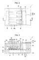
- Fig. 2 is a plan view of the recording head according to the first embodiment.
- Fig. 3 is a sectional view of the recording head according to the first embodiment.
- Fig. 4 is a diagram showing the density of electron states of BiFeO 3 perfect crystal.
- Fig. 5 is a diagram showing the density of electron states when Bi of BiFeO 3 has a 12.5% defect in an A site.
- Fig. 6 is a diagram showing the density of electron states when 12.5% of Fe of BiFeO 3 at a B site is substituted with Bi.
- Fig. 7 is a diagram showing density of electron states when 12.5% of transition metal at the B site is substituted with Pb for Pb(Zr,Ti)O 3 .
- Fig. 8 is a diagram showing density of electron states when 4% of oxygen loss occurs in an oxygen site of BiFeO 3 .
- Fig. 9 is a schematic diagram illustrating hopping conduction in a crystal of complex oxide.
- Fig. 10 is a schematic diagram illustrating hopping conduction in a crystal of complex oxide according to the invention.
- Fig. 11 is a diagram showing density of electron states when 12.5% of oxygen of BiFeO 3 is substituted with nitrogen.
- Fig. 12 is a diagram showing density of electron states when 12.5% of Bi of BiFeO 3 at the A site is substituted with Ce.
- Fig. 13 is a diagram showing density of electron states when 12.5% of Fe of BiFeO 3 at the B site is substituted with Mn.
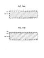
- Figs. 14A and 14B are sectional views showing a recording head manufacturing process according to the first embodiment.
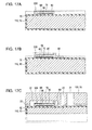
- Figs. 15A to 15C are sectional views showing the recording head manufacturing process according to the first embodiment.
- Figs. 16A and 16B are sectional views showing the recording head manufacturing process according to the first embodiment.
- Figs. 17A to 17C are sectional views showing the recording head manufacturing process according to the first embodiment.
- Figs. 18A and 18B are sectional views showing the recording head manufacturing process according to the first embodiment.
- Fig. 19 is a diagram showing a schematic configuration of a recording apparatus according to an embodiment of the invention.
- Fig. 1 an exploded perspective view showing a schematic configuration of an ink jet recording head which is an example of a liquid ejecting head according to a first embodiment of the invention.
- Fig. 2 is a plan view of Fig. 1
- Fig. 3 is a sectional view taken along the line III-III of Fig. 2 .
- a channel-formed substrate 10 of this embodiment is formed with a silicon single crystal substrate, and an elastic film 50 made of silicon dioxide is formed on one surface thereof.
- a plurality of pressure generating chambers 12 are installed to the channel-formed substrate 10 in the width direction thereof.
- a communication portion 13 is formed in the outer portion of the pressure generating chamber 12 of the channel-formed substrate 10 in the longitudinal direction so that each pressure generating chamber 12 communicates with the communication portion 13 via an ink supply path 14 and a communication path 15 installed for each pressure generating chamber 12.
- the communication portion 13 communicates with a manifold portion 31 of a protective substrate described later to configure a part of a manifold which becomes a common ink chamber of each pressure generating chamber 12.
- the ink supply path 14 is formed with a smaller width than the pressure generating chamber 12 so that a channel resistance of the ink introduced from the communication portion 13 to the pressure generating chamber 12 is maintained consistently.
- the ink supply path 14 is formed by squeezing the channel in the width direction from one side in this embodiment, it may also be formed by squeezing the channel in the width direction from both sides. In addition, the ink supply path may also be formed by squeezing the channel not in the width direction but in the thickness direction.
- a liquid channel composed of the pressure generating chamber 12, the communication portion 13, the ink supply path 14 and the communication path 15 is installed to the channel-formed substrate 10.
- a nozzle plate 20 in which a nozzle opening 21 communicating with the vicinity of the end portion of each pressure generating chamber 12 opposite to the ink supply path 14 is formed is adhered to the opening surface side of the channel-formed substrate 10 by means of an adhesive or thermal adhesion.
- the nozzle plate 20 is made of, for example, glass ceramics, silicon single crystal substrate, stainless steel, or the like.
- the elastic film 50 is formed at the side of the channel-formed substrate 10 opposite to the opening surface, as described above, and an adhesive film 56 made of titanium oxide with, for example, a thickness of about 30 to 50 nm to improve adhesion with the base of a first electrode 60 of the elastic film 50 is installed on the elastic film 50.
- an insulator film made of zirconium oxide may also be installed on the elastic film 50 as necessary.
- the first electrode 60, a thin-film piezoelectric layer 70 with a thickness of 2 ⁇ m or less, preferably 0.3 to 1.5 ⁇ m, and a second electrode 80 are laminated on the adhesion film 56 to configure a piezoelectric element 300.
- the piezoelectric element 300 is defined as including the first electrode 60, the piezoelectric layer 70 and the second electrode 80.
- any one electrode of the piezoelectric element 300 may be set to be a common electrode, and the electrode and the piezoelectric layer 70 are configured by patterning each pressure generating chamber 12.
- the first electrode 60 is set to be a common electrode of the piezoelectric element 300
- the second electrode 80 is set to be an individual electrode of the piezoelectric element 300, but this configuration may be set reversely in consideration of driving circuits or wirings.
- the piezoelectric element 300 and a vibration plate causing displacement by the operation of the corresponding piezoelectric element 300 are called an actuator device when combined.
- the elastic film 50, the adhesion film 56, the first electrode 60, and the insulator film which is provided as necessary serve as the vibration plate, but, for example, the elastic film 50 or the adhesion film 56 may not be provided without being limited to the above.
- the piezoelectric element 300 itself may be configured to substantially serve as the vibration plate.
- the Perovskite-type structure of the complex oxide including transition metal is written as ABO 3 .
- the A site and the B site respectively represent sites where oxygen is 12-coordinated and 6-coordinated.
- the piezoelectric layer 70 is made of complex oxide having the Perovskite-type structure containing bismuth (Bi) and ion (Fe), and therefore nitrogen is included at some oxygen sites.
- nitrogen is included at some oxygen sites.
- the complex oxide according to this embodiment may include bismuth at the A site of the Perovskite-type structure and iron at the B site, but the bismuth and iron at the A and B sites may be partially substituted with other elements.
- a substitution element for the A site may e.g. be lanthanum, praseodymium, neodymium, samarium or yttrium
- a substitution element of the B site may e.g. be cobalt, chrome, manganese, nickel or copper.
- Bismuth included in BiFeO 3 or the like may easily volatilize during a manufacturing process, particularly during a firing process of the piezoelectric layer, and may tend to cause crystal defects of the A site.
- the lost Bi may diffuse in the manufacturing chamber or toward the lower electrode.
- oxygen is lost in order to keep the electronic balance.
- the ratio of Bi defects to oxygen defects is 2:3 in order to satisfy the charge neutral principle.
- the presence of oxygen loss lowers the orbital energy of d electrons of the transition metal by means of Coulomb potential so that the band gap of the piezoelectric element is narrowed, which consequently becomes a direct factor causing leakage current.
- BiFeO 3 it may be considered to include an excess of Bi in advance in the stoichiometric composition, but the excess Bi is then released into not only the A site but also the B site unintentionally at a consistent rate. Bi released into the B site becomes a source of an electron carrier, which causes leakage current to the piezoelectric element. For this reason, in the system of BiFeO 3 , can be a disadvantage to use a manufacturing method where an excess of Bi is included in the stoichiometric composition.
- lead (Pb) may tend to volatilize during the manufacturing process, in a similar manner to Bi. For this reason, a method where an excess of Pb is included in the stoichiometric composition is used. The excessive Pb causes a phenomenon in which Pb is released into the B site unintentionally.
- the PZT as shown in Fig. 7 described later, even though Pb is unintentionally included in the B site, the band gap in the electron structure may be maintained.
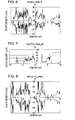
- Figs. 4 to 8 are diagrams showing density of electron states of each crystal, necessary for the first principle electron state calculation, where the horizontal axis represents an energy difference (eV) of electrons and the vertical axis represents density of electron states (DOS: Density Of State). In addition, a plus side greater than the state density 0 (/eV) represents up-spin, and a minus side represents down-spin.
- the ultra soft pseudopotential method based on the density functional approach in the range of the generalized gradient approximation (GGA) was used.
- the GGA+U method (GGA plus U method) was applied.
- the cutoffs of the wave function and the charge density were respectively 20 Hartree and 360 Hartree.
- the mesh at the inverse lattice point (k point) was (4x4x4).
- Fig. 4 is a diagram showing the density of electron states of a perfect crystal of bismuth ferric acid (BiFeO 3 ).
- Fig. 5 is a diagram showing the density of electron states when 12.5% of Bi at the A site of bismuth ferric acid (BiFeO 3 ) is defective.
- Fig. 6 is a diagram showing the density of electron states when 12.5% of Bi is included in the B site of bismuth ferric acid (BiFeO 3 ).
- Fig. 7 is a diagram showing the density of electron states when 12.5% of Pb is included in the B site of PZT.
- Fig. 8 is a diagram showing the density of electron states when a 4% loss occurs at the oxygen site of bismuth ferric acid (BiFeO 3 ).
- the system exhibits stable antiferromagnetic states in all of Figs. 4, 5 , 6, 7 and 8 .
- the highest electron occupancy level (Ef) is the top of the valence band, and therefore the band gap is opened to ensure insulation.
- a side state in a lower energy for the band gap is a charged band, and a side state in a higher energy is a conductive band.
- the highest electron occupancy level represents a level of the highest orbital energy occupied by electrons, which corresponds to one-electron energy capable of being obtained by the electron state simulation.
- 0 point of the horizontal axis is set to be the highest electron occupancy level (Ef).
- Fig. 7 the density of electron states where Pb is included in the B site in PZT is shown.
- the band gap in the electron structure may be maintained. Therefore, when Pb(Zr,Ti)O 3 is manufactured, even though a method of excessively including Pb in the stoichiometric composition in advance is used, the insulation of the piezoelectric body is not deteriorated.
- the occupied state density is shown at the minus side smaller than the energy of 0 eV.
- the highest electron occupancy level comes to be in the energy region of the conductive band. Therefore, the system is not insulating, and it could be understood that it becomes an n-type conductor as electron carriers are generated. At this time, it could be understood that the loss of the oxygen site gives two electron carriers, which require the area of the occupied state density.
- n-type defects and p-type defects coexist.
- a semiconductor since carriers in the conductive band and the charged band have a free electron state, hole carriers originating from p-type defects and electron carriers originating from n-type defects spread spatially, which may be negative to each other.
- transition metal oxide carriers of the conductive band and the charged band are local and have low mobility. For this reason, hole carriers and electron carriers do not perfectly offset each other. For this reason, in the transition metal oxide, the carriers which have not been offset contribute to electric conduction of the system as hopping conduction.
- Fig. 9 schematically shows the hopping conduction state in the transition metal compound where p-type defects and n-type defects are present.
- hopping conduction channels allowing movement of hole carriers and electron carriers are formed.
- the hopping conduction by one of both carriers may not be suppressed any more. This is estimated as a factor deteriorating insulation of BiFeO 3 .
- n-type dopant which offsets p-type defects or a p-type dopant which offsets n-type defects is doped to the A site or the B site, the generation of leakage current may be prevented, leakage may be prevented similar to the p-type result even when nitrogen is doped to the oxygen site, not to the A site or the B site.
- the invention is based on the above knowledge, and nitrogen is doped to the oxygen site of complex oxide, which is a transition metal compound such as BiFeO 3 , to prevent leakage current from occurring by n-type defects, thereby improving insulation.
- complex oxide which is a transition metal compound such as BiFeO 3
- nitrogen is doped at the oxygen site as described above, when compared with doping of metals at the A site or the B site, there is an advantage in that the piezoelectric characteristics of the complex oxide do not greatly change.
- FIG. 10 A schematic diagram of the hopping conduction in the transition metal compound of the invention where nitrogen is doped at the oxygen site is shown in Fig. 10 .
- Fig. 10 if nitrogen is doped to the oxygen site of complex oxide which is transition metal compound such as BiFeO 3 , n-type defects are offset by nitrogen doping. For this reason, the leakage current caused by hopping between the n-type defects may greatly decrease.
- nitrogen is doped at the oxygen site of e.g. BiFeO 3 , and the doped nitrogen becomes a p-type donor and offsets n-type defects.
- Fig. 11 is a diagram showing the density of electron states required for using the first principle electron state calculation, for the crystal where 5% of oxygen of the oxygen site is substituted with nitrogen.
- the conditions of the first principle electron state calculation are same as described above.
- Ef is located at the top of the valence band.
- a hole appears in the valence band.
- the nitrogen (N) element which substitutes a part of the oxygen site serves as a p-type donor. If integration is performed on the density of electron states with respect to the hole portion, it can be understood that the substitution of oxygen with nitrogen corresponds to the contribution of one hole.
- Ef is located at the bottom of the conductive band.
- Ce bismuth (Bi) of BiFeO 3
- Ce cerium
- Ef is located at the bottom of the conductive band.
- Mn manganese
- n-type defects can be offset by substituting a part of oxygen at the oxygen site of e.g. BiFeO 3 with nitrogen (N), thereby maintaining high insulation.
- p-type defects may also be offset by simultaneously doping with a dopant selected from at least one of cerium (Ce) and manganese (Mn).
- a dopant selected from at least one of cerium (Ce) and manganese (Mn).
- the dopant doped to the oxygen site is preferably introduced in an amount corresponding to the amount of expected n-type defects.
- the complex oxide may include lanthanum (which has a large ion radius) at the A site. Since lanthanum is included, it is possible to prevent a shape other than the Perovskite-type structure from appearing. Further, since lanthanum has a very weak covalent bonding property with the nearest oxygen, compared with bismuth, the potential barrier is lowered with respect to the rotation of polarization moment by an applied electric field. The situation where the rotation of polarization moment tends to occur improves the piezoelectric characteristics. In addition, lanthanum is metal with ion valence of +3, and therefore even though those metal elements are present in the A site, "valence balance" of the invention does not change, and the situation of leakage current is not adversely affected.
- lanthanum which has a large ion radius
- the content of lanthanum in the A site is preferably 5 to 20 mol% based on the total amount of bismuth, cerium and lanthanum.
- Praseodymium, neodymium, and samarium are also elements with large ion radii having ion valence of +3, and therefore give the same effect as lanthanum.
- the complex oxide may include cobalt (Co) and/or chromium (Cr), in addition to iron (Fe) at the B site.
- Such elements are preferably included in an amount of 12.5 to 87.5 mol% based on the total amount of the elements at the B site.
- the complex oxide includes iron, cobalt and chrome at a predetermined ratio at the location of the B site, insulation and magnetism may be maintained.
- the corresponding complex oxide since the corresponding complex oxide has a morphotropic phase boundary (MPB), it has excellent piezoelectric characteristics.
- the piezoelectric constant increases by the MPB, and therefore the piezoelectric characteristics are specially improved.
- the complex oxide preferably further includes barium titanate (for example, BaTiO 3 with the Perovskite-type structure) of the stoichiometric composition, in addition to BiFeO 3 .
- barium titanate for example, BaTiO 3 with the Perovskite-type structure
- BiFeO 3 barium titanate
- an MPB appears between BiFeO 3 with a rhomborhedral structure and BaTiO 3 with a tetragonal structure.
- the piezoelectric characteristic of the piezoelectric layer 70 is improved so that the vibration plate may make a big displacement just with a small voltage.
- the piezoelectric layer 70 includes barium titanate, for example, nitrogen is doped at the oxygen site of the complex oxide (for example, (Bi, Ba) (Fe, Ti)O 3 ) with the Perovskite-type structure formed with barium titanate and bismuth ferric acid which is a main component.
- the complex oxide for example, (Bi, Ba) (Fe, Ti)O 3
- the piezoelectric layer 70 of this embodiment has a monosymmetric crystal structure.
- the piezoelectric layer 70 made of the complex oxide with the Perovskite-type structure has a monoclinic symmetric property.
- This piezoelectric layer 70 may obtain a high piezoelectric property.
- a structure where the polarization moment of the piezoelectric layer may easily rotate may be conceived, regarding the electric field applied to a surface in the vertical direction.
- the piezoelectric layer the variation of the polarization moment is directly associated with the variation of the crystal structure, and therefore it securely comes to have the piezoelectric property. From the above, a high piezoelectric property may be obtained for the structure where polarization moment tends to change.
- the piezoelectric layer 70 preferably has an engineered domain arrangement in which the polarization direction is inclined by a predetermined angle (50 degrees to 60 degrees) to the vertical direction to the film surface (the thickness direction of the piezoelectric layer 70).
- a protective substrate 30 having the manifold portion 31 configuring at least a part of the manifold 100 is adhered by means of an adhesive 35 on the channel-formed substrate 10 where the piezoelectric element 300 is formed, namely on the first electrode 60, the elastic film 50, the insulator film prepared as necessary, or the lead electrode 90.
- the manifold portion 31 is formed to extend in the width direction of the pressure generating chamber 12 to pass through the thickness direction of the protective substrate 30 in this embodiment to communicate with the communication portion 13 of the channel-formed substrate 10 as described above, thereby configuring the manifold 100 which becomes a common ink chamber of each pressure generating chamber 12.
- the communication portion 13 of the channel-formed substrate 10 may be divided in plural for each pressure generating chamber 12, and only the manifold portion 31 may be used as the manifold. Further, for example, it is possible to provide only the pressure generating chamber 12 to the channel-formed substrate 10 so that the ink supply path 14 communicating with each pressure generating chamber 12 is provided to a member (for example, the elastic film 50, the insulator film prepared as necessary, or the like) interposed between the channel-formed substrate 10 and the protective substrate 30 as the manifold 100.
- a member for example, the elastic film 50, the insulator film prepared as necessary, or the like
- a piezoelectric element holding unit 32 with a space not disturbing the movement of the piezoelectric element 300 is installed in a region opposite to the piezoelectric element 300 of the protective substrate 30.
- the piezoelectric element holding unit 32 has a space not disturbing the movement of the piezoelectric element 300, and the space may be sealed or not sealed.
- the protective substrate 30 may be made of material with substantially the same coefficient thermal expansion as the channel-formed substrate 10, for example glass, ceramic material or the like, and in this embodiment, it is formed with a silicon single crystal substrate with the same material as the channel-formed substrate 10.
- a through hole 33 formed to pass through the protective substrate 30 in the thickness direction is formed in the protective substrate 30.
- the vicinity of the end portion of the lead electrode 90 appearing from the piezoelectric element 300 is installed to expose in the through hole 33.
- a driving circuit 120 for driving the installed piezoelectric element 300 is fixed on the protective substrate 30.
- the driving circuit 120 may use, for example, a circuit substrate, a semiconductor integrated circuit (IC), or the like.
- the driving circuit 120 and the lead electrode 90 are electrically connected via a connection wire 121 made of conductive wire such as bonding wire.
- a compliance substrate 40 composed of a sealing film 41 and a fixed plate 42 is adhered on the protective substrate 30.
- the sealing film 41 is made of material with flexibility and low rigidity, so that one side surface of the manifold portion 31 is sealed by the sealing film 41.
- the fixed plate 42 is made of relatively rigid material. Since a region of the fixed plate 42 opposite to the manifold 100 becomes an opening 43 perfectly removed in the thickness direction, the one side surface of the manifold 100 is sealed by only the sealing film 41 with flexibility.
- the ink is obtained from an ink inlet hole connected to an external ink supply unit (not shown) so that the inside is filled with the ink from the manifold 100 to the nozzle opening 21, and then voltage is applied between the first electrode 60 and the second electrode 80 respectively corresponding to the pressure generating chamber 12 according to the recording signal from the driving circuit 120 to flexural-deform the elastic film 50, the adhesion film 56, the first electrode 60 and the piezoelectric layer 70, so that the pressure in each pressure generating chamber 12 increases to discharge ink droplets from the nozzle opening 21.
- Figs. 14A to 18B are longitudinal sectional views of the pressure generating chamber.
- a silicon dioxide film made from silicon dioxide (SiO 2 ) or the like configuring the elastic film 50 is formed by thermal oxidation or the like on the surface of a wafer 110 for the channel-formed substrate which is a silicon wafer.
- an adhesion film 56 made from titanium oxide or the like is formed by thermal oxidation or the like on the elastic film 50 (the silicon dioxide film).
- a platinum film configuring the first electrode 60 is formed by sputtering or the like on the entire surface of the adhesion film 56.
- the piezoelectric layer 70 is laminated on the platinum film.
- the piezoelectric layer 70 may be a metal organic decomposition (MOD) method which obtains a piezoelectric layer (or, a piezoelectric film) made from metal oxide by applying and drying a solution containing a metal compound and firing at higher temperature, a chemical solution method such as a sol-gel method, or a vapor method such as sputtering.
- MOD metal organic decomposition
- the piezoelectric layer 70 may also be formed by methods such as laser ablation, spattering, pulse laser deposition (PLD), CVD, aerosol deposition, or the like, other than the above.
- a metal compound in detail, a sol or MOD solution (precursor solution) including a complex containing Bi and Fe, La contained as necessary or Co, Cr, cerium contained as necessary, and manganese at a desired composition ratio is applied on the first electrode 60 by spin coating to form a piezoelectric precursor film 71 (a coating process).
- a sol or MOD solution precursor solution including a complex containing Bi and Fe, La contained as necessary or Co, Cr, cerium contained as necessary, and manganese at a desired composition ratio is applied on the first electrode 60 by spin coating to form a piezoelectric precursor film 71 (a coating process).
- the applied precursor solution is obtained by mixing metal compounds containing Bi and Fe, wherein a Co, Cr, cerium, and/or manganese may optionally be contained so that each metal has a desired mole ratio, and dissolving or dispersing the corresponding mixture with a compound containing nitrogen in an organic solvent such as an alcohol or the like.
- the metal compounds may e.g. be an alkoxide, an organic acid salt, a ⁇ -diketone complex, or the like.
- the metal compound containing Bi may be, for example, 2-ethyl hexane acid bismuth or the like.
- the metal compound containing Fe may be, for example, 2-ethyl hexane acid iron or the like.
- the metal compound containing Co may be, for example, 2-ethyl hexane acid cobalt or the like.
- the metal compound containing Cr may be, for example, 2-ethyl hexane acid chrome or the like.
- the metal compound containing Mn may be, for example, 2-ethyl hexane acid manganese or the like.
- the metal compound containing La may be, for example, 2-ethyl hexane acid lanthanum or the like.
- the metal compound containing Ce may be, for example, 2-ethyle hexane acid cerium or the like.
- a metal compound containing two or more of Bi, Ce, Fe, Co, Mn, and La may also be used.
- the compound containing nitrogen may be ammonia, diethanol amine, or the like.
- the piezoelectric precursor film 71 is dried for a predetermined time (a drying process) by heating at predetermined temperature (150 to 400°C).
- a drying process a drying process
- the dried piezoelectric precursor film 71 is heated at predetermined temperature and kept for a predetermined time for dilapidation (a dilapidation process).
- the dilapidation used herein means to make organic components included in the piezoelectric precursor film 71 be separated as, for example, NO 2 , CO 2 , H 2 O or the like.
- the circumference of the drying process and the dilapidation process is not limited, but those processes may be performed in the atmosphere or in an inert gas.
- the piezoelectric precursor film 71 is crystallized by being heated at temperature of, for example, about 600 to 800°C, and kept for a predetermined time to form a piezoelectric film 72 (a firing process).
- a firing process the conditions are not limited, and this process may be performed in the atmosphere or in an inert gas.
- the heating device used for the drying process, the dilapidation process and the firing process may be, for example, a rapid thermal annealing (RTA) device for heating by the irradiation of infrared lamp, a hot plate or the like.
- RTA rapid thermal annealing
- the nitrogen content of nitrogen included in the piezoelectric film is investigated by the analysis using a secondary ion mass spectrometry (SIMS), the nitrogen content is preferably 0.01 moles or less per mole of the complex oxide, with an order of about 0.001 moles. If the nitrogen mole ratio is less than 0.0005, the effect of nitrogen as a p-type dopant is deteriorated.
- SIMS secondary ion mass spectrometry
- a register (not shown) of a predetermined shape is patterned on the piezoelectric film 72 as a mask so that the sides of the first electrode 60 and the piezoelectric film 72 are slanted with a first level.
- the register is peeled off, and then the coating process, the drying process and the dilapidation process, as described above, or the coating process, the drying process, the dilapidation process and the firing process are repeated several times according to a desired film thickness to form the piezoelectric layer 70 composed of a plurality of piezoelectric films 72, and therefore the piezoelectric layer 70 of a predetermined thickness composed of a plurality of piezoelectric films 72 is formed as shown in Fig. 16B .
- a film thickness obtained by one coating process of the coating solution is about 0.1 ⁇ m
- the film thickness of the entire piezoelectric layer 70 composed of ten layers of the piezoelectric films 72 becomes about 1.1 ⁇ m.
- the piezoelectric films 72 are laminated, it is also possible to use a single layer of the piezoelectric film 72.
- the second electrode 80 made of platinum or the like is formed on the piezoelectric layer 70 by sputtering or the like to pattern the piezoelectric layer 70 and the second electrode 80 together in a region opposite to each pressure generating chamber 12, and the piezoelectric element 300 is formed by the first electrode 60, the piezoelectric layer 70 and the second electrode 80.
- the patterning of the piezoelectric layer 70 and the second electrode 80 may be performed in a bundle by performing dry etching by means of a register (not shown) formed with a predetermined shape.
- post-annealing may be performed in a temperature range of 600°C to 800°C. By doing so, an excellent interface may be formed between the piezoelectric layer 70 and the first electrode 60 or the second electrode 80, and the crystalline property of the piezoelectric layer 70 may be improved.
- the lead electrode 90 made of, for example, gold (Au) or the like is formed on the entire surface of a wafer 110 for the channel-formed substrate, and then each piezoelectric element 300 is patterned by means of a mask pattern (not shown) made of, for example, register or the like.
- a wafer 130 for the protective substrate which is a silicon wafer and becomes a plurality of protective substrates 30, is adhered by means of the adhesive 35 to the piezoelectric element 300 of the wafer 110 for the channel-formed substrate, and then the wafer 110 for the channel-formed substrate is processed to have a predetermined thin thickness.
- a mask film 52 is newly formed on the wafer 110 for the channel-formed substrate to pattern a predetermined shape.
- anisotropic etching (wet etching) using an alkali solution such as KOH is performed to the wafer 110 for the channel-formed substrate by using the mask film 52 to form the pressure generating chamber 12, the communication portion 13, the ink supply path 14, the communication path 15 or the like, which correspond to the piezoelectric element 300.
- the channel-formed substrate 10 is a silicon single crystal substrate in the above embodiment, it may use, for example, an SOI substrate or material such as glass or the like, without being limited to the above.
- piezoelectric element 300 in which the first electrode 60, the piezoelectric layer 70 and the second electrode 80 are laminated in order on the substrate (the channel-formed substrate 10) is illustrated in the above embodiment, a vertical-vibrating piezoelectric element in which piezoelectric material and electrode-forming material are laminated with each other and extend or shrink in an axial direction may also be applied to the invention as an example, without being limited to the above.
- the ink jet recording head of these embodiments configures a part of a recording head unit having an ink channel communicating with an ink cartridge or the like and is loaded on an ink jet recording apparatus.
- Fig. 19 is a schematic view showing an example of the ink jet recording apparatus II.
- the recording head units 1A and 1B having the ink jet recording head I include cartridges 2A and 2B serving as an ink supply unit detachably installed thereto, and a cartridge 3 on which the recording head units 1A and 1B are loaded is installed to be movable in the axial direction of a cartridge shaft 5 mounted to an apparatus body 4.
- the recording head units 1A and 1B discharge, for example, black ink composition and color ink composition, respectively.
- a driving motor 6 is transferred to the cartridge 3 via a plurality of toothed wheels (not shown), and a timing belt 7, and the cartridge 3 on which the recording head units 1A and 1B are loaded moves along the cartridge shaft 5.
- a platen 8 is installed to the apparatus body 4 along the cartridge shaft 5 so that a recording sheet S which is a recording medium such as paper or the like fed by feeding rollers or the like (not shown) may be rolled around the platen 8 and carried out.
- the ink jet recording head units 1A and 1B respectively have a single ink jet recording head I, but one ink jet recording head unit 1A or 1B may have two or more ink jet recording heads as an example, without being limited to the above.
- the ink jet recording head is an example of the liquid ejecting head
- the invention is targeted at a broad range of liquid ejecting heads and may be applied to a liquid ejecting head which ejects liquid other than ink.
- Other liquid ejecting heads may include, for example, various kinds of recording heads used for an image recording apparatus such as a printer, color material ejecting heads used for making color filters of liquid crystal displays or the like, electrode material ejecting heads used for forming electrodes of organic EL displays, field emission displays (FED) or the like, biological organic substance ejecting heads used for making bio chips, or the like.
- the piezoelectric element of the invention may be applied to a piezoelectric element of a liquid ejecting head, which is representatively an ink jet recording head, as described above in order to show good insulation and piezoelectric characteristics, but it is not limited thereto.
- a piezoelectric element of a liquid ejecting head which is representatively an ink jet recording head, as described above in order to show good insulation and piezoelectric characteristics, but it is not limited thereto.
- it may be applied to piezoelectric elements of ultrasonic devices of ultrasonic transmitters, ultrasonic motors, piezoelectric transformers, and various sensors such as infrared sensors, ultrasonic sensors, temperature sensors, pressure sensors, pyroelectric sensors or the like.
- the invention may be applied to ferroelectric elements such as ferroelectric memories or the like in the same manner.
Landscapes
- Engineering & Computer Science (AREA)
- Manufacturing & Machinery (AREA)
- Chemical & Material Sciences (AREA)
- Dispersion Chemistry (AREA)
- Ceramic Engineering (AREA)
- Particle Formation And Scattering Control In Inkjet Printers (AREA)
Abstract
Description
- The present invention relates to a piezoelectric element and a liquid ejecting head and liquid ejecting device. The piezoelectric element can cause a pressure change in a pressure generating chamber communicating with a nozzle opening and having a piezoelectric layer and an electrode that applies a voltage to the piezoelectric layer.
- A piezoelectric actuator for a liquid ejecting head may use a piezoelectric element configured by interposing a piezoelectric layer made of piezoelectric material showing an electromechanical transduction function, for example, crystallized dielectric material, between two electrodes. As a representative example of the liquid ejecting head, there is an ink jet recording head in which a pressure generating chamber communicating with a nozzle opening discharging ink droplets is partially configured as a vibration plate so that the ink in the pressure generating chamber is pressed by transforming the vibration plate by the piezoelectric element to be discharged as ink droplets from the nozzle opening.
- The piezoelectric material used for the piezoelectric layer (piezoelectric ceramics) of the piezoelectric element requires high piezoelectric features, as a representative example of such lead zirconate titanate (PZT) is given (
JP-A-2001-223404 - However, from the viewpoint of environmental problems, piezoelectric materials with a reduced content of lead are demanded. As a piezoelectric material not containing lead, there is BiFeO3 having a Perovskite-type structure expressed by ABO3. Here, A and B of ABO3 represent an A site and a B site, which are respectively sites where oxygen is 12-coordinated and 6-coordinated. However, the BiFeO3-based piezoelectric material has low insulation and tends to cause a leakage current. If a leakage current tends to occur, particularly when a high voltage is applied, cracks may be generated, and so the material is not useful for the liquid ejecting head. A piezoelectric material may have high insulation of 1×10⁻³A/cm2 or less when a representative driving voltage of 25 V is applied.
- In addition, this problem is present not only in the ink jet recording head but also in other liquid ejecting heads which discharge liquid droplets other than ink and the piezoelectric element used for equipment other than the liquid ejecting heads. Further, the leakage current problem causes a serious problem of an increase in energy consumption when the piezoelectric element is used as a sensor. A low leakage current is desirable even for piezoelectric elements used for piezoelectric sensors, infrared sensors, temperature sensors and pyroelectric sensors to which a voltage of 1 V or less is applied.
- An advantage of some aspects of the invention is that it provides a piezoelectric element, a liquid ejecting head, and a liquid ejecting device which are environmentally friendly, and wherein the piezoelectric element has high insulation so that leakage current is suppressed.
- According to an aspect of the invention, there is provided a piezoelectric element which includes a piezoelectric layer and an electrode in connection with the piezoelectric layer, wherein the piezoelectric layer is made of complex oxide having a Perovskite-type structure ABO3 (wherein A is a 12-coordinated metal site, B is a 6-coordinated metal site and O is an oxygen site) containing bismuth and iron and wherein nitrogen is included at some oxygen sites.
- In this aspect, the piezoelectric element has high insulation so that leakage current is suppressed, resulting in great durability. In addition, since lead is not contained, the burden on the environment may decrease.
- It is preferable that nitrogen is included in an amount of 0.0005 to 0.01 moles per mole of the Perovskite-type complex oxide.
- In addition, it is preferable that bismuth is partially included at the B site.
- In addition, it is preferable that the complex oxide further comprises titanium and barium in addition to bismuth and iron. By doing so, the piezoelectric element has further superior piezoelectric characteristics (amount of deformation) .
- According to another aspect of the invention, there is provided a liquid ejectring head, which includes a pressure generating chamber communicating with a nozzle opening; and the above-defined piezoelectric element.
- In this aspect, since the piezoelectric element has high insulation due to the suppression of leakage current, it is possible to implement a liquid ejecting device with excellent durability. In addition, since lead is not contained, the burden on the environment may decrease.
- According to still another aspect of the invention, there is provided a liquid ejecting device including the liquid ejecting head of the above aspect.
- In this aspect, it is possible to implement a piezoelectric element with excellent insulation so that leakage current is suppressed. In addition, since lead is not contained, the burden on the environment is decreased.
- The invention will be described with reference to the accompanying drawings, wherein like numbers reference like elements.
-
Fig. 1 is an exploded perspective view showing a schematic configuration of a recording head according to a first embodiment. -
Fig. 2 is a plan view of the recording head according to the first embodiment. -
Fig. 3 is a sectional view of the recording head according to the first embodiment. -
Fig. 4 is a diagram showing the density of electron states of BiFeO3 perfect crystal. -
Fig. 5 is a diagram showing the density of electron states when Bi of BiFeO3 has a 12.5% defect in an A site. -
Fig. 6 is a diagram showing the density of electron states when 12.5% of Fe of BiFeO3 at a B site is substituted with Bi. -
Fig. 7 is a diagram showing density of electron states when 12.5% of transition metal at the B site is substituted with Pb for Pb(Zr,Ti)O3. -
Fig. 8 is a diagram showing density of electron states when 4% of oxygen loss occurs in an oxygen site of BiFeO3. -
Fig. 9 is a schematic diagram illustrating hopping conduction in a crystal of complex oxide. -
Fig. 10 is a schematic diagram illustrating hopping conduction in a crystal of complex oxide according to the invention. -
Fig. 11 is a diagram showing density of electron states when 12.5% of oxygen of BiFeO3 is substituted with nitrogen. -
Fig. 12 is a diagram showing density of electron states when 12.5% of Bi of BiFeO3 at the A site is substituted with Ce. -
Fig. 13 is a diagram showing density of electron states when 12.5% of Fe of BiFeO3 at the B site is substituted with Mn. -
Figs. 14A and 14B are sectional views showing a recording head manufacturing process according to the first embodiment. -
Figs. 15A to 15C are sectional views showing the recording head manufacturing process according to the first embodiment. -
Figs. 16A and 16B are sectional views showing the recording head manufacturing process according to the first embodiment. -
Figs. 17A to 17C are sectional views showing the recording head manufacturing process according to the first embodiment. -
Figs. 18A and 18B are sectional views showing the recording head manufacturing process according to the first embodiment. -
Fig. 19 is a diagram showing a schematic configuration of a recording apparatus according to an embodiment of the invention. -
Fig. 1 an exploded perspective view showing a schematic configuration of an ink jet recording head which is an example of a liquid ejecting head according to a first embodiment of the invention.Fig. 2 is a plan view ofFig. 1 , andFig. 3 is a sectional view taken along the line III-III ofFig. 2 . As shown inFigs. 1 to 3 , a channel-formedsubstrate 10 of this embodiment is formed with a silicon single crystal substrate, and anelastic film 50 made of silicon dioxide is formed on one surface thereof. - A plurality of
pressure generating chambers 12 are installed to the channel-formedsubstrate 10 in the width direction thereof. In addition, acommunication portion 13 is formed in the outer portion of thepressure generating chamber 12 of the channel-formedsubstrate 10 in the longitudinal direction so that eachpressure generating chamber 12 communicates with thecommunication portion 13 via anink supply path 14 and acommunication path 15 installed for eachpressure generating chamber 12. Thecommunication portion 13 communicates with amanifold portion 31 of a protective substrate described later to configure a part of a manifold which becomes a common ink chamber of eachpressure generating chamber 12. Theink supply path 14 is formed with a smaller width than thepressure generating chamber 12 so that a channel resistance of the ink introduced from thecommunication portion 13 to thepressure generating chamber 12 is maintained consistently. In addition, even though theink supply path 14 is formed by squeezing the channel in the width direction from one side in this embodiment, it may also be formed by squeezing the channel in the width direction from both sides. In addition, the ink supply path may also be formed by squeezing the channel not in the width direction but in the thickness direction. In this embodiment, a liquid channel composed of thepressure generating chamber 12, thecommunication portion 13, theink supply path 14 and thecommunication path 15 is installed to the channel-formedsubstrate 10. - In addition, a
nozzle plate 20 in which anozzle opening 21 communicating with the vicinity of the end portion of eachpressure generating chamber 12 opposite to theink supply path 14 is formed is adhered to the opening surface side of the channel-formedsubstrate 10 by means of an adhesive or thermal adhesion. In addition, thenozzle plate 20 is made of, for example, glass ceramics, silicon single crystal substrate, stainless steel, or the like. - Meanwhile, the
elastic film 50 is formed at the side of the channel-formedsubstrate 10 opposite to the opening surface, as described above, and anadhesive film 56 made of titanium oxide with, for example, a thickness of about 30 to 50 nm to improve adhesion with the base of afirst electrode 60 of theelastic film 50 is installed on theelastic film 50. In addition, an insulator film made of zirconium oxide may also be installed on theelastic film 50 as necessary. - Further, the
first electrode 60, a thin-film piezoelectric layer 70 with a thickness of 2 µm or less, preferably 0.3 to 1.5 µm, and asecond electrode 80 are laminated on theadhesion film 56 to configure apiezoelectric element 300. Here, thepiezoelectric element 300 is defined as including thefirst electrode 60, thepiezoelectric layer 70 and thesecond electrode 80. Generally, any one electrode of thepiezoelectric element 300 may be set to be a common electrode, and the electrode and thepiezoelectric layer 70 are configured by patterning eachpressure generating chamber 12. In this embodiment, thefirst electrode 60 is set to be a common electrode of thepiezoelectric element 300, and thesecond electrode 80 is set to be an individual electrode of thepiezoelectric element 300, but this configuration may be set reversely in consideration of driving circuits or wirings. In addition, here, thepiezoelectric element 300 and a vibration plate causing displacement by the operation of the correspondingpiezoelectric element 300 are called an actuator device when combined. In addition, in the above example, theelastic film 50, theadhesion film 56, thefirst electrode 60, and the insulator film which is provided as necessary serve as the vibration plate, but, for example, theelastic film 50 or theadhesion film 56 may not be provided without being limited to the above. In addition, thepiezoelectric element 300 itself may be configured to substantially serve as the vibration plate. - Hereinafter, the Perovskite-type structure of the complex oxide including transition metal is written as ABO3. Here, the A site and the B site respectively represent sites where oxygen is 12-coordinated and 6-coordinated.
- In this embodiment, the
piezoelectric layer 70 is made of complex oxide having the Perovskite-type structure containing bismuth (Bi) and ion (Fe), and therefore nitrogen is included at some oxygen sites. By so including nitrogem, as described later, leakage current is suppressed, and insulation is improved. In addition, since lead is not contained, the oxide is environmentally friendly. - The complex oxide according to this embodiment may include bismuth at the A site of the Perovskite-type structure and iron at the B site, but the bismuth and iron at the A and B sites may be partially substituted with other elements. For example, a substitution element for the A site may e.g. be lanthanum, praseodymium, neodymium, samarium or yttrium, and a substitution element of the B site may e.g. be cobalt, chrome, manganese, nickel or copper.
- Bismuth included in BiFeO3 or the like may easily volatilize during a manufacturing process, particularly during a firing process of the piezoelectric layer, and may tend to cause crystal defects of the A site. The lost Bi may diffuse in the manufacturing chamber or toward the lower electrode. As Bi is released, oxygen is lost in order to keep the electronic balance. The ratio of Bi defects to oxygen defects is 2:3 in order to satisfy the charge neutral principle. The presence of oxygen loss lowers the orbital energy of d electrons of the transition metal by means of Coulomb potential so that the band gap of the piezoelectric element is narrowed, which consequently becomes a direct factor causing leakage current. In order to suppress oxygen loss, it is desirable to suppress Bi loss. For this purpose, it may be considered to include an excess of Bi in advance in the stoichiometric composition, but the excess Bi is then released into not only the A site but also the B site unintentionally at a consistent rate. Bi released into the B site becomes a source of an electron carrier, which causes leakage current to the piezoelectric element. For this reason, in the system of BiFeO3, can be a disadvantage to use a manufacturing method where an excess of Bi is included in the stoichiometric composition.
- Here, in lead zirconate titanate (Pb(Zr,Ti)O3) which was used in the related art, lead (Pb) may tend to volatilize during the manufacturing process, in a similar manner to Bi. For this reason, a method where an excess of Pb is included in the stoichiometric composition is used.
The excessive Pb causes a phenomenon in which Pb is released into the B site unintentionally. However, in the PZT, as shown inFig. 7 described later, even though Pb is unintentionally included in the B site, the band gap in the electron structure may be maintained. For this reason, in a case where Pb(Zr,Ti)O3 is manufactured, even though a method where an excess of Pb is included in advance in the stoichiometric composition, the insulation of the piezoelectric body is not deteriorated. - After further investigating the above problems by using the first principle electron state calculation, the following findings were obtained.
-
Figs. 4 to 8 are diagrams showing density of electron states of each crystal, necessary for the first principle electron state calculation, where the horizontal axis represents an energy difference (eV) of electrons and the vertical axis represents density of electron states (DOS: Density Of State). In addition, a plus side greater than the state density 0 (/eV) represents up-spin, and a minus side represents down-spin. As the condition for the first principle electron state calculation, the ultra soft pseudopotential method based on the density functional approach in the range of the generalized gradient approximation (GGA) was used. For the transition metal atom of the B site, in order to give a strong correlation effect originated from the localization of the d electron orbit, the GGA+U method (GGA plus U method) was applied. The cutoffs of the wave function and the charge density were respectively 20 Hartree and 360 Hartree. The super cell of the crystal used for the calculation was configured by using an eight (2x2x2=8) ABO3 type Perovskite-type structure. In addition, the mesh at the inverse lattice point (k point) was (4x4x4). -
Fig. 4 is a diagram showing the density of electron states of a perfect crystal of bismuth ferric acid (BiFeO3).Fig. 5 is a diagram showing the density of electron states when 12.5% of Bi at the A site of bismuth ferric acid (BiFeO3) is defective.Fig. 6 is a diagram showing the density of electron states when 12.5% of Bi is included in the B site of bismuth ferric acid (BiFeO3).Fig. 7 is a diagram showing the density of electron states when 12.5% of Pb is included in the B site of PZT.Fig. 8 is a diagram showing the density of electron states when a 4% loss occurs at the oxygen site of bismuth ferric acid (BiFeO3). - The system exhibits stable antiferromagnetic states in all of
Figs. 4, 5 ,6, 7 and 8 . - As shown in
Fig. 4 , in the case of BiFeO3 perfect crystal, namely in a case where each site has no hole and Bi is not substituted with another element, the highest electron occupancy level (Ef) is the top of the valence band, and therefore the band gap is opened to ensure insulation. InFig. 4 , a side state in a lower energy for the band gap is a charged band, and a side state in a higher energy is a conductive band. - In addition, the highest electron occupancy level represents a level of the highest orbital energy occupied by electrons, which corresponds to one-electron energy capable of being obtained by the electron state simulation. In each graph of the density of electron states, 0 point of the horizontal axis is set to be the highest electron occupancy level (Ef).
- As shown in
Fig. 5 , for BiFeO3, if bismuth (Bi) of the A site is partially lost and causes defects, a hole state density is shown at the plus side greater than the energy of 0 eV. In other words, the highest electron occupancy level comes to be in the energy region of the valence band. Therefore, it could be understood that the insulation of the system is deteriorated to create hole carriers, and its electric conduction type is p type. At this time, it could be understood that the loss of Bi at the A site gives three hole carriers, which requires the area of the hole state density. - In addition, as shown in
Fig. 6 , if bismuth (Bi) is included at the B site, the state density occupied by the minus side smaller than the energy of 0 eV is shown. In other words, the highest electron occupancy level comes to be in the energy region of the conductive band. Therefore, the system is not insulating, and it could be understood that it becomes an n-type conductor since electron carriers are generated. At this time, it could be understood that inclusion of Bi at the B site gives one electron carrier, which requires the area of the occupied state density. - In
Fig. 7 , the density of electron states where Pb is included in the B site in PZT is shown. In the PZT-based piezoelectric material, even though Pb is unintentionally included in the B site, as shown inFig. 7 , the band gap in the electron structure may be maintained. Therefore, when Pb(Zr,Ti)O3 is manufactured, even though a method of excessively including Pb in the stoichiometric composition in advance is used, the insulation of the piezoelectric body is not deteriorated. - In addition, as shown in
Fig. 8 , if a 4% loss occurs in the oxygen site of BiFeO3, the occupied state density is shown at the minus side smaller than the energy of 0 eV. In other words, the highest electron occupancy level comes to be in the energy region of the conductive band. Therefore, the system is not insulating, and it could be understood that it becomes an n-type conductor as electron carriers are generated. At this time, it could be understood that the loss of the oxygen site gives two electron carriers, which require the area of the occupied state density. - Therefore, as shown in
Figs. 5 ,6 and 8 , in BiFeO3, n-type defects and p-type defects coexist. For example, in the case of a semiconductor, since carriers in the conductive band and the charged band have a free electron state, hole carriers originating from p-type defects and electron carriers originating from n-type defects spread spatially, which may be negative to each other. Meanwhile, in the case of transition metal oxide, carriers of the conductive band and the charged band are local and have low mobility. For this reason, hole carriers and electron carriers do not perfectly offset each other. For this reason, in the transition metal oxide, the carriers which have not been offset contribute to electric conduction of the system as hopping conduction. -
Fig. 9 schematically shows the hopping conduction state in the transition metal compound where p-type defects and n-type defects are present. As above, in the transition metal compound, for the p-type defects and the n-type defects, respectively, hopping conduction channels allowing movement of hole carriers and electron carriers are formed. In this circumstance, even though doping is conducted to compensate one of both carriers, the hopping conduction by one of both carriers may not be suppressed any more. This is estimated as a factor deteriorating insulation of BiFeO3. - For this, if an n-type dopant which offsets p-type defects or a p-type dopant which offsets n-type defects is doped to the A site or the B site, the generation of leakage current may be prevented, leakage may be prevented similar to the p-type result even when nitrogen is doped to the oxygen site, not to the A site or the B site.
- The invention is based on the above knowledge, and nitrogen is doped to the oxygen site of complex oxide, which is a transition metal compound such as BiFeO3, to prevent leakage current from occurring by n-type defects, thereby improving insulation. If nitrogen is doped at the oxygen site as described above, when compared with doping of metals at the A site or the B site, there is an advantage in that the piezoelectric characteristics of the complex oxide do not greatly change. In addition, to use the n-type dope element which prevents leak by p-type defects, for an example, it is preferred to further dope cerium (Ce) or manganese (Mn).
- A schematic diagram of the hopping conduction in the transition metal compound of the invention where nitrogen is doped at the oxygen site is shown in
Fig. 10 . As shown inFig. 10 , if nitrogen is doped to the oxygen site of complex oxide which is transition metal compound such as BiFeO3, n-type defects are offset by nitrogen doping. For this reason, the leakage current caused by hopping between the n-type defects may greatly decrease. - In other words, in the invention, nitrogen is doped at the oxygen site of e.g. BiFeO3, and the doped nitrogen becomes a p-type donor and offsets n-type defects.
-
Fig. 11 is a diagram showing the density of electron states required for using the first principle electron state calculation, for the crystal where 5% of oxygen of the oxygen site is substituted with nitrogen. In addition, the conditions of the first principle electron state calculation are same as described above. - As shown in
Fig. 11 , if a part of oxygen of BiFeO3 is forcibly substituted with nitrogen, Ef is located at the top of the valence band. In other words, a hole appears in the valence band. In other words, it could be understood that the nitrogen (N) element which substitutes a part of the oxygen site serves as a p-type donor. If integration is performed on the density of electron states with respect to the hole portion, it can be understood that the substitution of oxygen with nitrogen corresponds to the contribution of one hole. - In addition, as shown in
Fig. 12 , if 12.5% of bismuth (Bi) of BiFeO3 is forcibly substituted with cerium (Ce), Ef is located at the bottom of the conductive band. In other words, it could be understood that the Ce substitution of the A site serves as an n-type dopant. - In addition, as shown in
Fig. 13 , if 12.5% of Fe at the B site of BiFeO3 is forcibly substituted with manganese (Mn), Ef is located at the bottom of the conductive band. In other words, it can be understood that the Mn substitution of the B site serves as an n-type dopant. - As described above, in the invention, n-type defects can be offset by substituting a part of oxygen at the oxygen site of e.g. BiFeO3 with nitrogen (N), thereby maintaining high insulation.
- More preferably, p-type defects may also be offset by simultaneously doping with a dopant selected from at least one of cerium (Ce) and manganese (Mn). In other words, by substituting oxygen with nitrogen and doping with Ce and/or Mn, for both n-type and p-type hopping channels in the schematic diagram of
Fig. 9 , doping may be performed as if they are canceled. As a result, insulation may be maintained to be further higher. - The dopant doped to the oxygen site is preferably introduced in an amount corresponding to the amount of expected n-type defects.
- In the invention, the complex oxide may include lanthanum (which has a large ion radius) at the A site. Since lanthanum is included, it is possible to prevent a shape other than the Perovskite-type structure from appearing. Further, since lanthanum has a very weak covalent bonding property with the nearest oxygen, compared with bismuth, the potential barrier is lowered with respect to the rotation of polarization moment by an applied electric field. The situation where the rotation of polarization moment tends to occur improves the piezoelectric characteristics. In addition, lanthanum is metal with ion valence of +3, and therefore even though those metal elements are present in the A site, "valence balance" of the invention does not change, and the situation of leakage current is not adversely affected. The content of lanthanum in the A site is preferably 5 to 20 mol% based on the total amount of bismuth, cerium and lanthanum. Praseodymium, neodymium, and samarium are also elements with large ion radii having ion valence of +3, and therefore give the same effect as lanthanum.
- In addition, the complex oxide may include cobalt (Co) and/or chromium (Cr), in addition to iron (Fe) at the B site. Such elements are preferably included in an amount of 12.5 to 87.5 mol% based on the total amount of the elements at the B site. As described above, when the complex oxide includes iron, cobalt and chrome at a predetermined ratio at the location of the B site, insulation and magnetism may be maintained. In addition, since the corresponding complex oxide has a morphotropic phase boundary (MPB), it has excellent piezoelectric characteristics. In particular, when the cobalt and/or chrome are contained in a total amount of near 50 mol% with respect to the entire amount of iron, cobalt and chrome, for example, the piezoelectric constant increases by the MPB, and therefore the piezoelectric characteristics are specially improved.
- Further, the complex oxide preferably further includes barium titanate (for example, BaTiO3 with the Perovskite-type structure) of the stoichiometric composition, in addition to BiFeO3. In this case, at room temperature, an MPB appears between BiFeO3 with a rhomborhedral structure and BaTiO3 with a tetragonal structure. For this reason, the piezoelectric characteristic of the
piezoelectric layer 70 is improved so that the vibration plate may make a big displacement just with a small voltage. When thepiezoelectric layer 70 includes barium titanate, for example, nitrogen is doped at the oxygen site of the complex oxide (for example, (Bi, Ba) (Fe, Ti)O3) with the Perovskite-type structure formed with barium titanate and bismuth ferric acid which is a main component. - The
piezoelectric layer 70 of this embodiment has a monosymmetric crystal structure. In other words, thepiezoelectric layer 70 made of the complex oxide with the Perovskite-type structure has a monoclinic symmetric property. Thispiezoelectric layer 70 may obtain a high piezoelectric property. For this reason, a structure where the polarization moment of the piezoelectric layer may easily rotate may be conceived, regarding the electric field applied to a surface in the vertical direction. In the piezoelectric layer, the variation of the polarization moment is directly associated with the variation of the crystal structure, and therefore it securely comes to have the piezoelectric property. From the above, a high piezoelectric property may be obtained for the structure where polarization moment tends to change. - In addition, the
piezoelectric layer 70 preferably has an engineered domain arrangement in which the polarization direction is inclined by a predetermined angle (50 degrees to 60 degrees) to the vertical direction to the film surface (the thickness direction of the piezoelectric layer 70). - A
lead electrode 90 made of, for example, gold (Au) which is extracted from the vicinity of the end portion of theink supply path 14 side and in connection with theelastic film 50, or even onto an insulator film which is prepared as necessary, is connected to eachsecond electrode 80 which is an individual electrode of thepiezoelectric element 300. - A
protective substrate 30 having themanifold portion 31 configuring at least a part of the manifold 100 is adhered by means of an adhesive 35 on the channel-formedsubstrate 10 where thepiezoelectric element 300 is formed, namely on thefirst electrode 60, theelastic film 50, the insulator film prepared as necessary, or thelead electrode 90. Themanifold portion 31 is formed to extend in the width direction of thepressure generating chamber 12 to pass through the thickness direction of theprotective substrate 30 in this embodiment to communicate with thecommunication portion 13 of the channel-formedsubstrate 10 as described above, thereby configuring the manifold 100 which becomes a common ink chamber of eachpressure generating chamber 12. In addition, thecommunication portion 13 of the channel-formedsubstrate 10 may be divided in plural for eachpressure generating chamber 12, and only themanifold portion 31 may be used as the manifold. Further, for example, it is possible to provide only thepressure generating chamber 12 to the channel-formedsubstrate 10 so that theink supply path 14 communicating with eachpressure generating chamber 12 is provided to a member (for example, theelastic film 50, the insulator film prepared as necessary, or the like) interposed between the channel-formedsubstrate 10 and theprotective substrate 30 as themanifold 100. - In addition, a piezoelectric
element holding unit 32 with a space not disturbing the movement of thepiezoelectric element 300 is installed in a region opposite to thepiezoelectric element 300 of theprotective substrate 30. The piezoelectricelement holding unit 32 has a space not disturbing the movement of thepiezoelectric element 300, and the space may be sealed or not sealed. - The
protective substrate 30 may be made of material with substantially the same coefficient thermal expansion as the channel-formedsubstrate 10, for example glass, ceramic material or the like, and in this embodiment, it is formed with a silicon single crystal substrate with the same material as the channel-formedsubstrate 10. - In addition, A through
hole 33 formed to pass through theprotective substrate 30 in the thickness direction is formed in theprotective substrate 30. In addition, the vicinity of the end portion of thelead electrode 90 appearing from thepiezoelectric element 300 is installed to expose in the throughhole 33. - In addition, a driving
circuit 120 for driving the installedpiezoelectric element 300 is fixed on theprotective substrate 30. The drivingcircuit 120 may use, for example, a circuit substrate, a semiconductor integrated circuit (IC), or the like. In addition, the drivingcircuit 120 and thelead electrode 90 are electrically connected via aconnection wire 121 made of conductive wire such as bonding wire. - In addition, a
compliance substrate 40 composed of a sealingfilm 41 and a fixedplate 42 is adhered on theprotective substrate 30. Here, the sealingfilm 41 is made of material with flexibility and low rigidity, so that one side surface of themanifold portion 31 is sealed by the sealingfilm 41. In addition, the fixedplate 42 is made of relatively rigid material. Since a region of the fixedplate 42 opposite to the manifold 100 becomes anopening 43 perfectly removed in the thickness direction, the one side surface of the manifold 100 is sealed by only the sealingfilm 41 with flexibility. - In the ink jet recording head I of this embodiment, the ink is obtained from an ink inlet hole connected to an external ink supply unit (not shown) so that the inside is filled with the ink from the manifold 100 to the
nozzle opening 21, and then voltage is applied between thefirst electrode 60 and thesecond electrode 80 respectively corresponding to thepressure generating chamber 12 according to the recording signal from the drivingcircuit 120 to flexural-deform theelastic film 50, theadhesion film 56, thefirst electrode 60 and thepiezoelectric layer 70, so that the pressure in eachpressure generating chamber 12 increases to discharge ink droplets from thenozzle opening 21. - Next, an example of a method of manufacturing the ink jet recording head according to this embodiment will be described with reference to
Figs. 14A to 18B . In addition,Figs. 14A to 18B are longitudinal sectional views of the pressure generating chamber. - First, as shown in
Fig. 14A , a silicon dioxide film made from silicon dioxide (SiO2) or the like configuring theelastic film 50 is formed by thermal oxidation or the like on the surface of awafer 110 for the channel-formed substrate which is a silicon wafer. Then, as shown inFig. 14B , anadhesion film 56 made from titanium oxide or the like is formed by thermal oxidation or the like on the elastic film 50 (the silicon dioxide film). - Next, as shown in
Fig. 15A , a platinum film configuring thefirst electrode 60 is formed by sputtering or the like on the entire surface of theadhesion film 56. - After that, the
piezoelectric layer 70 is laminated on the platinum film. Thepiezoelectric layer 70 may be a metal organic decomposition (MOD) method which obtains a piezoelectric layer (or, a piezoelectric film) made from metal oxide by applying and drying a solution containing a metal compound and firing at higher temperature, a chemical solution method such as a sol-gel method, or a vapor method such as sputtering. In addition, thepiezoelectric layer 70 may also be formed by methods such as laser ablation, spattering, pulse laser deposition (PLD), CVD, aerosol deposition, or the like, other than the above. - Regarding the detailed forming order example of the
piezoelectric layer 70, first, as shown inFig. 15B , a metal compound, in detail, a sol or MOD solution (precursor solution) including a complex containing Bi and Fe, La contained as necessary or Co, Cr, cerium contained as necessary, and manganese at a desired composition ratio is applied on thefirst electrode 60 by spin coating to form a piezoelectric precursor film 71 (a coating process). - The applied precursor solution is obtained by mixing metal compounds containing Bi and Fe, wherein a Co, Cr, cerium, and/or manganese may optionally be contained so that each metal has a desired mole ratio, and dissolving or dispersing the corresponding mixture with a compound containing nitrogen in an organic solvent such as an alcohol or the like.
- The metal compounds may e.g. be an alkoxide, an organic acid salt, a β-diketone complex, or the like.
- The metal compound containing Bi may be, for example, 2-ethyl hexane acid bismuth or the like. The metal compound containing Fe may be, for example, 2-ethyl hexane acid iron or the like. The metal compound containing Co may be, for example, 2-ethyl hexane acid cobalt or the like. The metal compound containing Cr may be, for example, 2-ethyl hexane acid chrome or the like. The metal compound containing Mn may be, for example, 2-ethyl hexane acid manganese or the like. The metal compound containing La may be, for example, 2-ethyl hexane acid lanthanum or the like. The metal compound containing Ce may be, for example, 2-ethyle hexane acid cerium or the like. In addition, a metal compound containing two or more of Bi, Ce, Fe, Co, Mn, and La may also be used. In addition, the compound containing nitrogen may be ammonia, diethanol amine, or the like.
- After that, the
piezoelectric precursor film 71 is dried for a predetermined time (a drying process) by heating at predetermined temperature (150 to 400°C). Next, the driedpiezoelectric precursor film 71 is heated at predetermined temperature and kept for a predetermined time for dilapidation (a dilapidation process). In addition, the dilapidation used herein means to make organic components included in thepiezoelectric precursor film 71 be separated as, for example, NO2, CO2, H2O or the like. The circumference of the drying process and the dilapidation process is not limited, but those processes may be performed in the atmosphere or in an inert gas. - Next, as shown in
Fig. 15C , thepiezoelectric precursor film 71 is crystallized by being heated at temperature of, for example, about 600 to 800°C, and kept for a predetermined time to form a piezoelectric film 72 (a firing process). In the firing process, the conditions are not limited, and this process may be performed in the atmosphere or in an inert gas. - In addition, the heating device used for the drying process, the dilapidation process and the firing process may be, for example, a rapid thermal annealing (RTA) device for heating by the irradiation of infrared lamp, a hot plate or the like.
- At this time, if the content of nitrogen included in the piezoelectric film is investigated by the analysis using a secondary ion mass spectrometry (SIMS), the nitrogen content is preferably 0.01 moles or less per mole of the complex oxide, with an order of about 0.001 moles. If the nitrogen mole ratio is less than 0.0005, the effect of nitrogen as a p-type dopant is deteriorated.
- Next, as shown in
Fig. 16A , a register (not shown) of a predetermined shape is patterned on thepiezoelectric film 72 as a mask so that the sides of thefirst electrode 60 and thepiezoelectric film 72 are slanted with a first level. - After that, the register is peeled off, and then the coating process, the drying process and the dilapidation process, as described above, or the coating process, the drying process, the dilapidation process and the firing process are repeated several times according to a desired film thickness to form the
piezoelectric layer 70 composed of a plurality ofpiezoelectric films 72, and therefore thepiezoelectric layer 70 of a predetermined thickness composed of a plurality ofpiezoelectric films 72 is formed as shown inFig. 16B . For example, in a case where a film thickness obtained by one coating process of the coating solution is about 0.1 µm, for example, the film thickness of the entirepiezoelectric layer 70 composed of ten layers of thepiezoelectric films 72 becomes about 1.1 µm. In addition, in this embodiment, even though thepiezoelectric films 72 are laminated, it is also possible to use a single layer of thepiezoelectric film 72. - After the
piezoelectric layer 70 is formed as described above, as shown inFig. 17A , thesecond electrode 80 made of platinum or the like is formed on thepiezoelectric layer 70 by sputtering or the like to pattern thepiezoelectric layer 70 and thesecond electrode 80 together in a region opposite to eachpressure generating chamber 12, and thepiezoelectric element 300 is formed by thefirst electrode 60, thepiezoelectric layer 70 and thesecond electrode 80. In addition, the patterning of thepiezoelectric layer 70 and thesecond electrode 80 may be performed in a bundle by performing dry etching by means of a register (not shown) formed with a predetermined shape. After that, as necessary, post-annealing may be performed in a temperature range of 600°C to 800°C. By doing so, an excellent interface may be formed between thepiezoelectric layer 70 and thefirst electrode 60 or thesecond electrode 80, and the crystalline property of thepiezoelectric layer 70 may be improved. - Next, as shown in
Fig. 17B , thelead electrode 90 made of, for example, gold (Au) or the like is formed on the entire surface of awafer 110 for the channel-formed substrate, and then eachpiezoelectric element 300 is patterned by means of a mask pattern (not shown) made of, for example, register or the like. - Next, as shown in
Fig. 17C , a wafer 130 for the protective substrate, which is a silicon wafer and becomes a plurality ofprotective substrates 30, is adhered by means of the adhesive 35 to thepiezoelectric element 300 of thewafer 110 for the channel-formed substrate, and then thewafer 110 for the channel-formed substrate is processed to have a predetermined thin thickness. - Next, as shown in
Fig. 18A , amask film 52 is newly formed on thewafer 110 for the channel-formed substrate to pattern a predetermined shape. - In addition, as shown in
Fig. 18B , anisotropic etching (wet etching) using an alkali solution such as KOH is performed to thewafer 110 for the channel-formed substrate by using themask film 52 to form thepressure generating chamber 12, thecommunication portion 13, theink supply path 14, thecommunication path 15 or the like, which correspond to thepiezoelectric element 300. - After that, unnecessary portions in the outer circumferences of the
wafer 110 for the channel-formed substrate and the wafer 130 for the protective substrate are cut off by, for example, dicing or the like and removed. In addition, themask film 52 at the surface of thewafer 110 for the channel-formed substrate, which is opposite to the wafer 130 for the protective substrate, is removed, and then thenozzle plate 20 in which thenozzle opening 21 is formed is adhered thereto, and simultaneously, thecompliance substrate 40 is adhered to the wafer 130 for the protective substrate so that thewafer 110 for the channel-formed substrate or the like is divided into the channel-formedsubstrates 10 with a tip size as shown inFig. 1 , thereby manufacturing the ink jet recording head I of this embodiment. - Heretofore, one embodiment of the invention has been described, but the basic configuration of the invention is not limited to the above description. For example, even though the channel-formed
substrate 10 is a silicon single crystal substrate in the above embodiment, it may use, for example, an SOI substrate or material such as glass or the like, without being limited to the above. - Further, even though the
piezoelectric element 300 in which thefirst electrode 60, thepiezoelectric layer 70 and thesecond electrode 80 are laminated in order on the substrate (the channel-formed substrate 10) is illustrated in the above embodiment, a vertical-vibrating piezoelectric element in which piezoelectric material and electrode-forming material are laminated with each other and extend or shrink in an axial direction may also be applied to the invention as an example, without being limited to the above. - In addition, the ink jet recording head of these embodiments configures a part of a recording head unit having an ink channel communicating with an ink cartridge or the like and is loaded on an ink jet recording apparatus.
Fig. 19 is a schematic view showing an example of the ink jet recording apparatus II. - As shown in
Fig. 19 , therecording head units cartridges cartridge 3 on which therecording head units cartridge shaft 5 mounted to an apparatus body 4. Therecording head units - In addition, the driving force of a driving
motor 6 is transferred to thecartridge 3 via a plurality of toothed wheels (not shown), and a timing belt 7, and thecartridge 3 on which therecording head units cartridge shaft 5. Meanwhile, aplaten 8 is installed to the apparatus body 4 along thecartridge shaft 5 so that a recording sheet S which is a recording medium such as paper or the like fed by feeding rollers or the like (not shown) may be rolled around theplaten 8 and carried out. - In the example shown in
Fig. 19 , the ink jetrecording head units recording head unit - In addition, even though it has been described in the above embodiment that the ink jet recording head is an example of the liquid ejecting head, the invention is targeted at a broad range of liquid ejecting heads and may be applied to a liquid ejecting head which ejects liquid other than ink. Other liquid ejecting heads may include, for example, various kinds of recording heads used for an image recording apparatus such as a printer, color material ejecting heads used for making color filters of liquid crystal displays or the like, electrode material ejecting heads used for forming electrodes of organic EL displays, field emission displays (FED) or the like, biological organic substance ejecting heads used for making bio chips, or the like.
- The piezoelectric element of the invention may be applied to a piezoelectric element of a liquid ejecting head, which is representatively an ink jet recording head, as described above in order to show good insulation and piezoelectric characteristics, but it is not limited thereto. For example, it may be applied to piezoelectric elements of ultrasonic devices of ultrasonic transmitters, ultrasonic motors, piezoelectric transformers, and various sensors such as infrared sensors, ultrasonic sensors, temperature sensors, pressure sensors, pyroelectric sensors or the like. In addition, the invention may be applied to ferroelectric elements such as ferroelectric memories or the like in the same manner.
Claims (6)
- A piezoelectric element comprising:a piezoelectric layer; andan electrode in connection with the piezoelectric layer,wherein the piezoelectric layer comprises complex oxide having a Perovskite-type structure ABO3 (wherein A is a 12-coordinated metal site, B is a 6-coordinated metal site and O is an oxygen site) comprising bismuth and iron and wherein nitrogen is included at some oxygen sites.
- The piezoelectric element according to claim 1, wherein nitrogen is included in an amount of 0.0005 to 0.01 moles per mole of the Perovskite-type complex oxide.
- The piezoelectric element according to claim 1 or claim 2, wherein bismuth is partially included at a B site.
- The piezoelectric element according to any preceding claim, wherein the complex oxide further comprises titanium and barium in addition to bismuth and iron.
- A liquid ejecting head comprising:a pressure generating chamber communicating with a nozzle opening; anda piezoelectric element as defined in any preceding claim.
- A liquid ejecting device comprising the liquid ejecting head according to claim 5.
Applications Claiming Priority (1)
| Application Number | Priority Date | Filing Date | Title |
|---|---|---|---|
| JP2010294297A JP2012139920A (en) | 2010-12-28 | 2010-12-28 | Liquid ejection head, liquid ejection apparatus and piezoelectric element |
Publications (2)
| Publication Number | Publication Date |
|---|---|
| EP2472622A2 true EP2472622A2 (en) | 2012-07-04 |
| EP2472622A3 EP2472622A3 (en) | 2015-01-28 |
Family
ID=45406532
Family Applications (1)
| Application Number | Title | Priority Date | Filing Date |
|---|---|---|---|
| EP20110195574 Withdrawn EP2472622A3 (en) | 2010-12-28 | 2011-12-23 | Liquid ejecting head, liquid ejecting device and piezoelectric element |
Country Status (4)
| Country | Link |
|---|---|
| US (1) | US8746853B2 (en) |
| EP (1) | EP2472622A3 (en) |
| JP (1) | JP2012139920A (en) |
| CN (1) | CN102555479A (en) |
Families Citing this family (2)
| Publication number | Priority date | Publication date | Assignee | Title |
|---|---|---|---|---|
| JP6950709B2 (en) * | 2017-01-06 | 2021-10-13 | コニカミノルタ株式会社 | Inkjet head and image forming equipment |
| CN114262222B (en) * | 2021-12-31 | 2022-10-14 | 中国科学院上海硅酸盐研究所 | Method for regulating resistivity and polarization strength of bismuth ferrite-barium titanate-based piezoelectric ceramic material |
Family Cites Families (20)
| Publication number | Priority date | Publication date | Assignee | Title |
|---|---|---|---|---|
| JPH02186614A (en) * | 1989-01-12 | 1990-07-20 | Seiko Epson Corp | Method of treating ferroelectric film |
| CN1033384C (en) * | 1993-01-15 | 1996-11-27 | 山东大学 | Preparation method of bismuth titanate ferroelectric film |
| JPH104181A (en) * | 1996-06-17 | 1998-01-06 | Sharp Corp | Ferroelectric element and semiconductor device |
| JP3730840B2 (en) * | 1999-08-20 | 2006-01-05 | 松下電器産業株式会社 | Dielectric film and manufacturing method thereof |
| JP4051654B2 (en) | 2000-02-08 | 2008-02-27 | セイコーエプソン株式会社 | Piezoelectric element, ink jet recording head, manufacturing method thereof, and ink jet printer |
| JP4004205B2 (en) * | 2000-03-23 | 2007-11-07 | 独立行政法人科学技術振興機構 | Manufacturing method of low resistance p-type SrTiO3 |
| JP2004292180A (en) * | 2003-03-25 | 2004-10-21 | Hiroshi Irie | Ferroelectric material, and method of manufacturing the same |
| WO2005122260A1 (en) * | 2004-06-11 | 2005-12-22 | Fujitsu Limited | Capacitive element, integrated circuit and electronic device |
| GB0421120D0 (en) * | 2004-09-22 | 2004-10-27 | Goodrich Control Sys Ltd | Piezoelectric materials |
| JP4793568B2 (en) * | 2005-07-08 | 2011-10-12 | セイコーエプソン株式会社 | Actuator device, liquid jet head, and liquid jet device |
| JP4988179B2 (en) * | 2005-09-22 | 2012-08-01 | ローム株式会社 | Zinc oxide compound semiconductor device |
| JP4785187B2 (en) * | 2006-02-20 | 2011-10-05 | 富士通セミコンダクター株式会社 | Semiconductor device and manufacturing method of semiconductor device |
| JP2007266346A (en) * | 2006-03-29 | 2007-10-11 | Seiko Epson Corp | Piezoelectric thin film, piezoelectric element, droplet ejecting head, droplet ejecting apparatus, and method for manufacturing droplet ejecting head |
| JP5035504B2 (en) * | 2006-04-12 | 2012-09-26 | セイコーエプソン株式会社 | Inkjet recording head and inkjet printer |
| JP4775772B2 (en) * | 2008-04-01 | 2011-09-21 | セイコーエプソン株式会社 | Piezoelectric material and piezoelectric element |
| CN101367671B (en) * | 2008-09-12 | 2011-01-12 | 济南大学 | Lead-free double-layer ferroelectric composite film for high-temperature piezoelectric devices and preparation method thereof |
| JP5414433B2 (en) * | 2008-09-30 | 2014-02-12 | キヤノン株式会社 | Ferroelectric ceramic material |
| US8400047B2 (en) * | 2009-03-12 | 2013-03-19 | Canon Kabushiki Kaisha | Piezoelectric material, piezoelectric device, and method of producing the piezoelectric device |
| US8405285B2 (en) * | 2009-06-08 | 2013-03-26 | Fujifilm Corporation | Piezoelectric device, piezoelectric actuator having the same, liquid discharge apparatus, and power generating apparatus |
| JP5660274B2 (en) * | 2010-01-05 | 2015-01-28 | セイコーエプソン株式会社 | Liquid ejecting head manufacturing method, piezoelectric element manufacturing method, liquid ejecting head, liquid ejecting apparatus, and piezoelectric element |
-
2010
- 2010-12-28 JP JP2010294297A patent/JP2012139920A/en not_active Withdrawn
-
2011
- 2011-12-23 EP EP20110195574 patent/EP2472622A3/en not_active Withdrawn
- 2011-12-23 CN CN2011104392253A patent/CN102555479A/en active Pending
- 2011-12-27 US US13/338,055 patent/US8746853B2/en not_active Expired - Fee Related
Also Published As
| Publication number | Publication date |
|---|---|
| US8746853B2 (en) | 2014-06-10 |
| CN102555479A (en) | 2012-07-11 |
| US20120162321A1 (en) | 2012-06-28 |
| EP2472622A3 (en) | 2015-01-28 |
| JP2012139920A (en) | 2012-07-26 |
Similar Documents
| Publication | Publication Date | Title |
|---|---|---|
| EP2472623B1 (en) | Liquid ejecting head, liquid ejecting apparatus and piezoelectric element | |
| US8646879B2 (en) | Piezoelectric element, liquid ejecting head, and liquid ejecting apparatus | |
| US8573754B2 (en) | Methods for manufacturing liquid ejecting head and piezoelectric element, liquid ejecting head, liquid ejecting apparatus, and piezoelectric element | |
| US8662644B2 (en) | Liquid ejecting head and liquid ejecting apparatus, and piezoelectric element | |
| EP3379589B1 (en) | Piezoelectric film element | |
| US8608297B2 (en) | Piezoelectric element, liquid ejecting head, and liquid ejecting apparatus | |
| CN102529371B (en) | Liquid ejecting head, liquid ejecting apparatus, and piezoelectric element | |
| US9312791B2 (en) | Piezoelectric element, liquid ejecting head, liquid ejecting apparatus, ultrasonic sensor, piezoelectric motor, and power generating apparatus | |
| JP5610134B2 (en) | Liquid ejecting head, liquid ejecting apparatus, and piezoelectric element | |
| US8746853B2 (en) | Piezoelectric element, liquid ejecting head, liquid ejecting apparatus | |
| JP5610133B2 (en) | Liquid ejecting head, liquid ejecting apparatus, and piezoelectric element | |
| JP5928675B2 (en) | Liquid ejecting head, liquid ejecting apparatus, piezoelectric element, ultrasonic sensor and infrared sensor | |
| US8876259B2 (en) | Liquid ejecting head, liquid ejecting apparatus and piezoelectric element | |
| JP5440795B2 (en) | Liquid ejecting head, liquid ejecting apparatus, and piezoelectric element | |
| JP2011238708A (en) | Liquid ejection head manufacturing method, liquid ejection device, and piezoelectric element manufacturing method | |
| US8608294B2 (en) | Piezoelectric element, liquid ejecting head, and liquid ejecting apparatus | |
| JP5743059B2 (en) | Liquid ejecting head, liquid ejecting apparatus, piezoelectric element, ultrasonic sensor and infrared sensor |
Legal Events
| Date | Code | Title | Description |
|---|---|---|---|
| AK | Designated contracting states |
Kind code of ref document: A2 Designated state(s): AL AT BE BG CH CY CZ DE DK EE ES FI FR GB GR HR HU IE IS IT LI LT LU LV MC MK MT NL NO PL PT RO RS SE SI SK SM TR |
|
| AX | Request for extension of the european patent |
Extension state: BA ME |
|
| PUAI | Public reference made under article 153(3) epc to a published international application that has entered the european phase |
Free format text: ORIGINAL CODE: 0009012 |
|
| PUAL | Search report despatched |
Free format text: ORIGINAL CODE: 0009013 |
|
| AK | Designated contracting states |
Kind code of ref document: A3 Designated state(s): AL AT BE BG CH CY CZ DE DK EE ES FI FR GB GR HR HU IE IS IT LI LT LU LV MC MK MT NL NO PL PT RO RS SE SI SK SM TR |
|
| AX | Request for extension of the european patent |
Extension state: BA ME |
|
| RIC1 | Information provided on ipc code assigned before grant |
Ipc: H01L 41/08 20060101ALI20141223BHEP Ipc: H01L 41/187 20060101AFI20141223BHEP Ipc: B41J 2/16 20060101ALI20141223BHEP |
|
| 17P | Request for examination filed |
Effective date: 20150714 |
|
| RBV | Designated contracting states (corrected) |
Designated state(s): AL AT BE BG CH CY CZ DE DK EE ES FI FR GB GR HR HU IE IS IT LI LT LU LV MC MK MT NL NO PL PT RO RS SE SI SK SM TR |
|
| GRAP | Despatch of communication of intention to grant a patent |
Free format text: ORIGINAL CODE: EPIDOSNIGR1 |
|
| INTG | Intention to grant announced |
Effective date: 20151215 |
|
| RIN1 | Information on inventor provided before grant (corrected) |
Inventor name: TAMURA, HIROAKI Inventor name: MIYAZAWA, HIROMU |
|
| STAA | Information on the status of an ep patent application or granted ep patent |
Free format text: STATUS: THE APPLICATION IS DEEMED TO BE WITHDRAWN |
|
| 18D | Application deemed to be withdrawn |
Effective date: 20160426 |