EP2472569A1 - Diffusion agent composition, method of forming impurity diffusion layer, and solar cell - Google Patents
Diffusion agent composition, method of forming impurity diffusion layer, and solar cell Download PDFInfo
- Publication number
- EP2472569A1 EP2472569A1 EP10811467A EP10811467A EP2472569A1 EP 2472569 A1 EP2472569 A1 EP 2472569A1 EP 10811467 A EP10811467 A EP 10811467A EP 10811467 A EP10811467 A EP 10811467A EP 2472569 A1 EP2472569 A1 EP 2472569A1
- Authority
- EP
- European Patent Office
- Prior art keywords
- agent composition
- diffusing
- diffusing agent
- impurity diffusion
- semiconductor substrate
- Prior art date
- Legal status (The legal status is an assumption and is not a legal conclusion. Google has not performed a legal analysis and makes no representation as to the accuracy of the status listed.)
- Granted
Links
Images


Classifications
-
- H—ELECTRICITY
- H10—SEMICONDUCTOR DEVICES; ELECTRIC SOLID-STATE DEVICES NOT OTHERWISE PROVIDED FOR
- H10F—INORGANIC SEMICONDUCTOR DEVICES SENSITIVE TO INFRARED RADIATION, LIGHT, ELECTROMAGNETIC RADIATION OF SHORTER WAVELENGTH OR CORPUSCULAR RADIATION
- H10F10/00—Individual photovoltaic cells, e.g. solar cells
-
- H—ELECTRICITY
- H10—SEMICONDUCTOR DEVICES; ELECTRIC SOLID-STATE DEVICES NOT OTHERWISE PROVIDED FOR
- H10P—GENERIC PROCESSES OR APPARATUS FOR THE MANUFACTURE OR TREATMENT OF DEVICES COVERED BY CLASS H10
- H10P32/00—Diffusion of dopants within, into or out of wafers, substrates or parts of devices
- H10P32/10—Diffusion of dopants within, into or out of semiconductor bodies or layers
- H10P32/16—Diffusion of dopants within, into or out of semiconductor bodies or layers between a solid phase and a liquid phase
-
- H—ELECTRICITY
- H10—SEMICONDUCTOR DEVICES; ELECTRIC SOLID-STATE DEVICES NOT OTHERWISE PROVIDED FOR
- H10F—INORGANIC SEMICONDUCTOR DEVICES SENSITIVE TO INFRARED RADIATION, LIGHT, ELECTROMAGNETIC RADIATION OF SHORTER WAVELENGTH OR CORPUSCULAR RADIATION
- H10F10/00—Individual photovoltaic cells, e.g. solar cells
- H10F10/10—Individual photovoltaic cells, e.g. solar cells having potential barriers
- H10F10/14—Photovoltaic cells having only PN homojunction potential barriers
-
- H—ELECTRICITY
- H10—SEMICONDUCTOR DEVICES; ELECTRIC SOLID-STATE DEVICES NOT OTHERWISE PROVIDED FOR
- H10F—INORGANIC SEMICONDUCTOR DEVICES SENSITIVE TO INFRARED RADIATION, LIGHT, ELECTROMAGNETIC RADIATION OF SHORTER WAVELENGTH OR CORPUSCULAR RADIATION
- H10F71/00—Manufacture or treatment of devices covered by this subclass
- H10F71/121—The active layers comprising only Group IV materials
-
- H—ELECTRICITY
- H10—SEMICONDUCTOR DEVICES; ELECTRIC SOLID-STATE DEVICES NOT OTHERWISE PROVIDED FOR
- H10P—GENERIC PROCESSES OR APPARATUS FOR THE MANUFACTURE OR TREATMENT OF DEVICES COVERED BY CLASS H10
- H10P32/00—Diffusion of dopants within, into or out of wafers, substrates or parts of devices
- H10P32/10—Diffusion of dopants within, into or out of semiconductor bodies or layers
- H10P32/14—Diffusion of dopants within, into or out of semiconductor bodies or layers within a single semiconductor body or layer in a solid phase; between different semiconductor bodies or layers, both in a solid phase
-
- H—ELECTRICITY
- H10—SEMICONDUCTOR DEVICES; ELECTRIC SOLID-STATE DEVICES NOT OTHERWISE PROVIDED FOR
- H10P—GENERIC PROCESSES OR APPARATUS FOR THE MANUFACTURE OR TREATMENT OF DEVICES COVERED BY CLASS H10
- H10P32/00—Diffusion of dopants within, into or out of wafers, substrates or parts of devices
- H10P32/10—Diffusion of dopants within, into or out of semiconductor bodies or layers
- H10P32/19—Diffusion sources
-
- Y—GENERAL TAGGING OF NEW TECHNOLOGICAL DEVELOPMENTS; GENERAL TAGGING OF CROSS-SECTIONAL TECHNOLOGIES SPANNING OVER SEVERAL SECTIONS OF THE IPC; TECHNICAL SUBJECTS COVERED BY FORMER USPC CROSS-REFERENCE ART COLLECTIONS [XRACs] AND DIGESTS
- Y02—TECHNOLOGIES OR APPLICATIONS FOR MITIGATION OR ADAPTATION AGAINST CLIMATE CHANGE
- Y02E—REDUCTION OF GREENHOUSE GAS [GHG] EMISSIONS, RELATED TO ENERGY GENERATION, TRANSMISSION OR DISTRIBUTION
- Y02E10/00—Energy generation through renewable energy sources
- Y02E10/50—Photovoltaic [PV] energy
- Y02E10/547—Monocrystalline silicon PV cells
-
- Y—GENERAL TAGGING OF NEW TECHNOLOGICAL DEVELOPMENTS; GENERAL TAGGING OF CROSS-SECTIONAL TECHNOLOGIES SPANNING OVER SEVERAL SECTIONS OF THE IPC; TECHNICAL SUBJECTS COVERED BY FORMER USPC CROSS-REFERENCE ART COLLECTIONS [XRACs] AND DIGESTS
- Y02—TECHNOLOGIES OR APPLICATIONS FOR MITIGATION OR ADAPTATION AGAINST CLIMATE CHANGE
- Y02P—CLIMATE CHANGE MITIGATION TECHNOLOGIES IN THE PRODUCTION OR PROCESSING OF GOODS
- Y02P70/00—Climate change mitigation technologies in the production process for final industrial or consumer products
- Y02P70/50—Manufacturing or production processes characterised by the final manufactured product
Definitions
- the present invention relates to a diffusing agent composition, a method of forming an impurity diffusion layer, and a solar cell.
- a P-type or N-type impurity diffusion layer is formed in a semiconductor substrate by forming a coating film on a surface of the semiconductor substrate using a diffusing agent that contains an impurity diffusion component and then by causing the impurity diffusion component to diffuse from the coating film of the diffusing agent into the semiconductor substrate.
- a spin coating method is often used as a method for applying a diffusing agent on a surface of a semiconductor substrate.
- a screen printing method a screen (printing plate) of mesh-like silk, synthetic resins, stainless steel, or the like is first stretched on a frame, and a part that allows a diffusing agent to pass and a part that does not allow a diffusing agent to pass are formed on the screen.
- the diffusing agent is then applied to the screen, and the applied diffusing agent is pushed out onto a surface of a semiconductor substrate using a squeegee. With this, the diffusing agent is transferred onto the surface of the semiconductor substrate, thereby forming a coating film of the diffusing agent in a predetermined pattern, line, or the like on the surface of the semiconductor substrate.
- a printing roller (printing plate) on which a groove is formed along the circumference thereof and a pressing roller for pressing a semiconductor substrate against the printing roller are arranged facing each other at a short distance. Then, the printing roller and the pressing roller are rotated in directions opposite from each other while feeding the diffusing agent into the groove, and the semiconductor substrate is allowed to pass between these rollers. With this, the printing roller and the semiconductor substrate come into contact with each other with pressure, and the diffusing agent filling the groove of the printing roller is transferred onto the surface of the semiconductor substrate, thereby forming a coating film of the diffusing agent in a predetermined pattern, line, or the like on the surface of the semiconductor substrate.
- Patent Document No. 1 describes a dopant paste (diffusing agent composition) for use in these printing methods.
- Patent Document No. 1 JP 2002-539615 (published Japanese translation of PCT international publication for patent application)
- diffusing agents used for the screen printing method and roll coat printing method are required to be hard to dry while having a predetermined viscosity.
- diffusing agents there is always a demand for the improvement of the ability to create a precise coating film form (pattern) when applied on the surface of a semiconductor, i.e., coating film formability, and the ability to uniformly diffuse over a predetermined region of the semiconductor substrate so as to reduce a resistance value at a diffusion region to a desired value, i.e., diffusibility.
- a purpose of the present invention is to provide: a diffusing agent composition that can be preferably employed for a screen printing method and a roll coat printing method having excellent coating film formability and diffusibility; a method of forming an impurity diffusion layer using the diffusing agent composition; and a solar cell.
- a diffusing agent composition according to one embodiment of the present invention that is used to print an impurity diffusion component onto a semiconductor substrate, comprises: an impurity diffusion component (A); a binder resin (B) configured to thermally decompose and disappear below a temperature, at which the impurity-diffusing component (A) starts diffusing thermally; a SiO 2 fine particle (C); and an organic solvent (D) configured to contain an organic solvent (D1) having a boiling point of at least 100 degrees Celsius.
- a diffusing agent composition can be obtained that can be preferably employed for a screen printing method and a roll coat printing method having excellent coating film formability and diffusibility.
- Another embodiment of the present invention relates to a method for forming an impurity diffusion layer, and the method for forming an impurity diffusion layer comprises: forming a coating film by printing the diffusing agent composition according to the above embodiment; and diffusing the impurity diffusion component (A) of the diffusing agent composition into a semiconductor substrate.
- an impurity diffusion layer can be formed with higher accuracy.
- Yet another embodiment of the present invention relates to a solar cell, and the solar cell comprises a semiconductor substrate in which an impurity diffusion layer is formed by the method of forming an impurity diffusion layer of the embodiment.
- a diffusing agent composition that can be preferably employed for a screen printing method and a roll coat printing method having excellent coating film formability and diffusibility, a method of forming an impurity diffusion layer using the diffusing agent composition, and a solar cell can be provided.
- the diffusing agent composition according to the present embodiment is used to print an impurity-diffusing component onto a semiconductor substrate and contains an impurity-diffusing component (A), a binder resin (B), SiO 2 fine particles (C), and an organic solvent (D).
- A impurity-diffusing component
- B binder resin
- C SiO 2 fine particles
- D organic solvent
- the impurity-diffusing component (A) is a compound generally used as a dopant for manufacturing a solar cell.
- the impurity diffusion component (A) is an N-type impurity diffusion component containing a compound of an element in the Group V (the Group 15) or a P-type impurity diffusion component containing a compound of an element in the Group III (the Group 13).
- the impurity diffusion component (A) allows for the formation of an N-type or P-type impurity diffusion layer (impurity diffusion region) in a semiconductor substrate.
- the N-type impurity-diffusing component containing a compound of an element in the Group V allows for the formation, in a process of forming an electrode of a solar cell, of an N-type impurity diffusion layer in a P-type semiconductor substrate and an N + -type (high concentration N-type) impurity diffusion layer in an N-type semiconductor substrate.
- Examples of the compound of an element in the Group V contained in the impurity-diffusing component (A) include P 2 O 5 Bi 2 O 3 , Sb(OCH 2 CH 3 ) 3 , SbCl 3 , As(OC 4 H 9 ) 3 , or the like, and the impurity-diffusing component (A) contains at least one kind of these compounds.
- the P-type impurity-diffusing component containing a compound of an element in the Group III allows for the formation, in a process of forming an electrode of a solar cell, of a P-type impurity diffusion layer in an N-type semiconductor substrate and a P + -type (high concentration P-type) impurity diffusion layer in a P-type semiconductor substrate.
- Examples of the compound of an element in the Group III contained in the impurity-diffusing component (A) include B 2 O 3 , Al 2 O 3 , or the like, and the impurity-diffusing component (A) contains at least one kind of these compounds.
- the amount of the impurity-diffusing component (A) to be added is appropriately adjusted in accordance with, for example, the thickness of an impurity diffusion layer formed in a semiconductor substrate.
- the amount of the impurity-diffusing component (A) to be added is preferably 5 to 60 percent by mass and more preferably 15 to 50 percent by mass with respect to the entire mass of the solid components of the impurity-diffusing component (A), the binder resin (B), and the SiO 2 fine particles (C) (when the mass of the solid components is set to be 100).
- the amount of the impurity-diffusing component (A) to be added is at least 5 percent by mass, further improved diffusibility can be obtained.
- the amount of the impurity-diffusing component (A) to be added is 60 percent by mass or less, a more stable solution and further improved coating film formability can be obtained.
- the binder resin (B) has a property of allowing the impurity-diffusing component (A) to diffuse well. Therefore, the binder resin (B) plays a role of allowing the impurity-diffusing component (A) to diffuse uniformly in a diffusing agent composition and thereby allowing the impurity-diffusing component (A) to diffuse uniformly on the surface of a semiconductor substrate.
- the binder resin (B) thermally decomposes and disappears below a temperature, at which the impurity-diffusing component (A) starts diffusing thermally. Therefore, carbon is not left on the surface of the semiconductor substrate when the impurity-diffusing component (A) diffuses thermally. This prevents a situation where carbon diffuses in the semiconductor substrate along with the thermal diffusion of the impurity-diffusing component (A) and which prevents a desired resistance value from being obtained or which causes a variation in the resistance value.
- such a binder resin (B) allows for the improvement of the diffusibility of a diffusing agent composition and for the adjustment of the resistance value at a region of a semiconductor substrate, where the diffusing agent composition has diffused, to a desired value with high accuracy.
- the "temperature, at which the impurity-diffusing component (A) starts diffusing thermally” is a temperature at which an impurity-diffusing component starts entering inside the semiconductor substrate from the surface of the semiconductor substrate, e.g., a temperature at which the impurity-diffusing component has entered inside the semiconductor substrate by an amount of about 10 nm and preferably about 1 nm from the boundary between the semiconductor substrate and the diffusing agent composition.
- binder resin (B) thermally decomposes and disappears means, e.g., a situation where the binder resin loses about 95 percent, preferably about 99 percent, and most preferably 100 percent of the entire mass of the binder resin.
- the binder resin (B) is preferably a resin whose decomposition temperature is below a temperature, which is lower than the temperature at which the impurity-diffusing component (A) starts diffusing thermally by 200 degrees Celsius, or a resin whose decomposition temperature is below 400 degrees Celsius. Also, the binder resin (B) is preferably a resin, 80 percent by mass of which thermally decomposes at a heating temperature of 500 degrees Celsius. According to these, prevention of a condition where there is a carbon residue at the time of the thermal diffusion of the impurity-diffusing component (A) can be further ensured.
- the "decomposition temperature” is a temperature at which the mass of the binder resin starts to decrease, e.g., a temperature at which the binder resin is reduced by about 5 percent and preferably about 1 percent of the entire mass of the binder resin.
- the binder resin (B) is preferably a non-silicon resin. If the binder resin (B) is a silicon resin, a diffusing agent composition attached to a printing plate of a screen printing machine or a roll coater may be fixed to the printing plate when dried. In order to remove the diffusing agent composition fixed to the printing plate, it is necessary to wash the printing plate using hydrofluoric acid (HF). In this case, the hydrofluoric acid attached to the printing plate may attach to metal parts of a printing machine and decompose these metal parts. In addition, since hydrofluoric acid is deleterious, a risk associated with the operation of removing the diffusing agent composition will be increased.
- HF hydrofluoric acid
- the diffusing agent composition dried on the printing plate can be washed off using an organic solvent such as acetone, isobutanol, or the like. Therefore, the diffusing agent composition according to the present embodiment can be easily handled.
- the binder resin (B) contains an acrylic resin.
- the acrylic resin contained in the binder resin (B) preferably has a butyral group.
- Specific examples of the binder resin (B) include an acrylic resin composed of a polymerizable monomer such as methyl methacrylate (MMA), methacrylic acid (MAA), isobutyl methacrylate (i-BMA), tertiary-butyl methacrylate (t-BMA), acrylic acid, ethyl acrylate, methyl acrylate, butyl acrylate, hydroxyethyl acrylate, hydroxypropyl acrylate, isobutyl acrylate, ethyl methacrylate, butyl methacrylate, hydroxypropyl methacrylate, or the like.
- MMA methyl methacrylate
- MAA methacrylic acid
- i-BMA isobutyl methacrylate
- t-BMA tertiary-butyl meth
- the amount of the binder resin (B) to be added is preferably 5 to 60 percent by mass and more preferably 15 to 50 percent by mass with respect to the entire mass of the solid components of the impurity-diffusing component (A), the binder resin (B), and the SiO 2 fine particles (C).
- the amount of the binder resin (B) to be added is at least 5 percent by mass, the coating film formability becomes further improved such that a uniform coating film (printing film) can be formed. Thus, further improved diffusibility can be obtained.
- the amount of the binder resin (B) to be added is 60 percent by mass or less, a more stable solution and further improved diffusibility can be obtained.
- SiO 2 fine particles (C) are added as filler.
- the compatibility of the impurity-diffusing component (A) with the binder resin (B) can be improved by the addition of the SiO 2 fine particles (C).
- the impurity-diffusing component (A) can be more uniformly applied on the surface of a semiconductor substrate.
- the impurity-diffusing component (A) can be more uniformly diffused on the semiconductor substrate. Therefore, the diffusibility of a diffusing agent composition can be improved by the SiO 2 fine particles (C).
- the average particle size is preferably about 1 ⁇ m or less.
- the SiO 2 fine particles (C) include fumed silica and the like.
- the amount of the SiO 2 fine particles (C) to be added is preferably 5 to 60 percent by mass and more preferably 15 to 50 percent by mass with respect to the entire mass of the solid components of the impurity-diffusing component (A), the binder resin (B), and the SiO 2 fine particles (C).
- the amount of the SiO 2 fine particles (C) to be added is at least 5 percent by mass, a more stable solution and further improved diffusibility can be obtained.
- the amount of the SiO 2 fine particles (C) to be added is 60 percent by mass or less, further improved coating film formability and further improved diffusibility can be obtained. If the SiO 2 fine particles (C) are not added, a solution is not likely to be stabilized, and mottling of a coating film is caused. Thus, good diffusibility cannot be obtained.
- An organic solvent (D) contains an organic solvent (D1) having a boiling point of at least 100 degrees Celsius. Since the boiling point of the organic solvent (D1) is at least 100 degrees Celsius, a diffusing agent composition can be prevented from becoming dry. Thus, when the diffusing agent composition is applied to a printing plate used for a roll coat printing method and a screen printing method, a situation can be prevented where the diffusing agent composition becomes dry and fixed on the printing plate. Therefore, by containing the organic solvent (D), the generation of print cracking on a coating film printed onto a semiconductor substrate can be prevented. In other words, the coating film formability of the diffusing agent composition is improved by the organic solvent (D).
- the organic solvent (D) preferably contains the organic solvent (D1) such that the organic solvent (D1) accounts for at least 10 percent by mass of the entire mass of the organic solvent (D).
- the amount of the organic solvent (D1) contained in the organic solvent (D) is less than 10 percent by mass, an obtained drying prevention effect is small, and there is a possibility that print cracking is generated on a coating film formed on the surface of a semiconductor substrate.
- the organic solvent (D1) includes ethylene glycol monomethyl ether, ethylene glycol monoethyl ether, ethylene glycol monopropyl ether, ethylene glycol monobutyl ether, ethylene glycol dimethyl ether, ethylene glycol diethyl ether, ethylene glycol dipropyl ether, propylene glycol monomethyl ether, propylene glycol monoethyl ether, propylene glycol monopropyl ether, propylene glycol monobutyl ether, propylene glycol dimethyl ether, propylene glycol diethyl ether, diethylene glycol monomethyl ether, diethylene glycol monoethyl ether, diethylene glycol monophenyl ether, diethylene glycol dimethyl ether, diethylene glycol diethyl ether, triethylene glycol monomethyl ether, triethylene glycol monoethyl ether, triethylene glycol dimethyl ether, triethylene glycol dimethyl ether, triethylene glycol dimethyl ether, triethylene glycol
- the organic solvent (D) includes a mixture of the above-stated organic solvent (D1) and ethanol, isopropanol, methyl ethyl ketone, acetone, ethyl acetate, methanol, n-hexane, cyclohexane, or the like.
- the concentration of a metallic impurity contained in the diffusing agent composition is preferably 500 ppm or less. This can suppress a decrease in the efficiency of a photovoltaic effect, which is caused by the inclusion of the metallic impurity.
- the diffusing agent composition according to the present embodiment may contain a commonly-used surface-active agent, antifoaming agent, or the like as another additive agent.
- the ratio of the solid components (solid content concentration) with respect to the entire mass of the diffusing agent composition can be appropriately changed based on a printing method and is preferably 5 to 90 percent by mass.
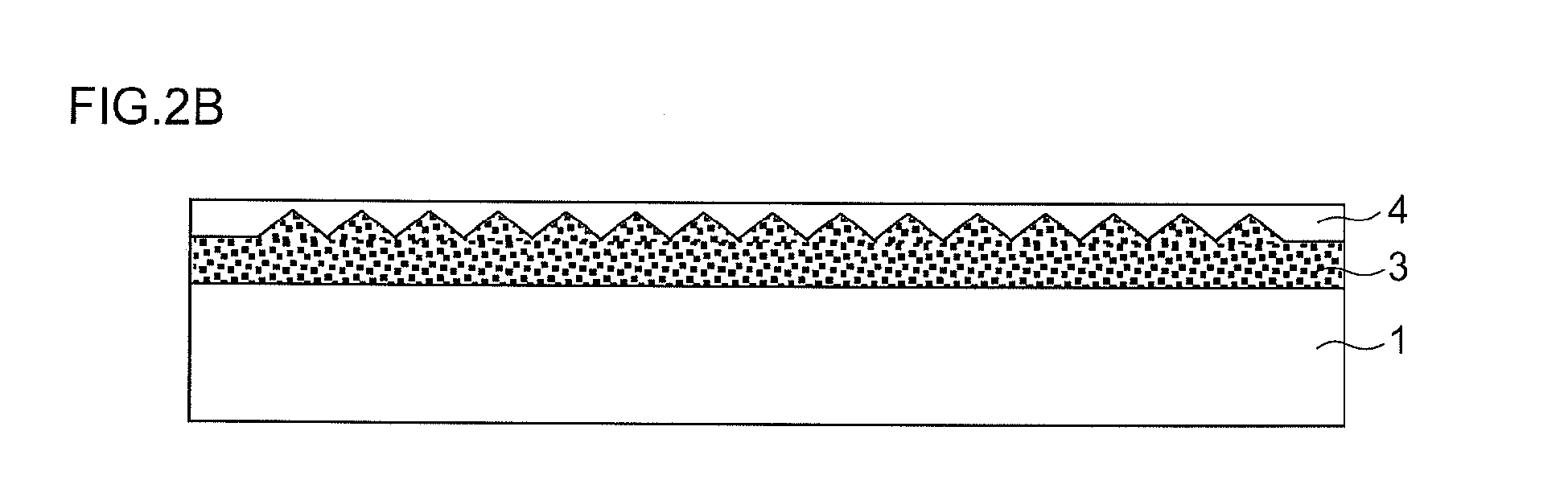
- Fig. 1A through Fig. 1D and Fig. 2A through Fig. 2D are process sectional views for explaining a method of manufacturing a solar cell including a method of forming an impurity diffusion layer according to an embodiment of the invention.
- a method of forming an N-type impurity diffusion layer in a P-type semiconductor substrate is explained as an example.
- a P-type impurity diffusion layer can be formed in an N-type semiconductor substrate.
- the method of forming an impurity diffusion layer comprises: a step of forming a coating film by printing the above-described diffusing agent composition containing an impurity-diffusing component (A) onto a semiconductor substrate; and a step of diffusing the impurity-diffusing component (A) contained in the diffusing agent composition into the semiconductor substrate.
- a P-type semiconductor substrate 1 such as a silicon substrate is prepared first.
- a texture portion 1a having a fine relief structure is formed on one main surface of the semiconductor substrate 1 by a well-known wet etching method.
- the texture portion 1a prevents reflection of light on the surface of the semiconductor substrate 1.
- a diffusing agent composition 2 containing an N-type impurity-diffusing component (A) as described above is applied onto the main surface of the semiconductor substrate 1 on the side of the texture portion 1a.
- the diffusing agent composition 2 is applied onto the surface of the semiconductor substrate 1 by a roll coat printing method or a screen printing method.
- a roll coat printing method a printing roller provided on a well-known roll coater is filled with the diffusing agent composition 2, and the diffusing agent composition 2 is printed onto the semiconductor substrate 1 by allowing the semiconductor substrate 1 to pass between the printing roller and a roller arranged to face the printing roller.
- the diffusing agent composition 2 is applied to a screen provided on a well-known screen printing machine, and the diffusing agent composition 2 is printed onto the semiconductor substrate 1 by pushing out the diffusing agent composition 2 onto the surface of the semiconductor substrate 1 using a squeegee. After a coating film is formed as described above, the applied diffusing agent composition 2 is dried using a well-known means such as an oven.
- the semiconductor substrate 1 on which the diffusing agent composition 2 is applied is placed inside an electric furnace and then burned.
- the N-type impurity-diffusing component (A) in the diffusing agent composition 2 is allowed to diffuse into the semiconductor substrate 1 through the surface of the semiconductor substrate 1 in the electric furnace.
- the semiconductor substrate 1 may be heated by commonly-used laser irradiation. In this way, the N-type impurity diffusion component (A) is diffused into the semiconductor substrate 1 to form an N-type impurity diffusion layer 3.
- the diffusing agent composition 2 is then removed by a well-known etching method.
- a passivation film 4 composed of a silicon nitride film (SiN film) is formed on the main surface of the semiconductor substrate 1 on the side of the texture portion 1a using a well-known chemical vapor deposition method (CVD method), e.g., a plasma CVD method.
- CVD method chemical vapor deposition method
- the passivation film 4 also functions as an antireflective film.
- a pattern of a surface electrode 5 is made on the main surface of the semiconductor substrate 1 on the side of the passivation film 4 by screen printing a silver (Ag) paste.
- the surface electrode 5 is formed into, e.g., a comb-shaped pattern, etc., to improve the efficiency of a solar cell.
- a backside electrode 6 is formed on the other main surface of the semiconductor substrate 1 by screen printing an aluminum (Al) paste.
- the semiconductor substrate 1 on which the backside electrode 6 is formed is placed inside an electric furnace and then burned, and aluminum forming the backside electrode 6 then diffuses into the semiconductor substrate 1. This allows for the reduction in electrical resistance on the side of the backside electrode 6. With these steps, a solar cell 10 according to the embodiment can be manufactured.
- the diffusing agent composition according to the present embodiment contains: the impurity-diffusing component (A); the binder resin (B) that thermally decomposes and disappears below a temperature, at which the impurity-diffusing component (A) starts diffusing thermally; the SiO 2 fine particles (C); and the organic solvent (D) that contains the organic solvent (D1) having a boiling point of at least 100 degrees Celsius. Therefore, the diffusing agent composition according to the present embodiment leaves almost no carbon residue at the time of the thermal diffusion of the impurity-diffusing component (A) and has high diffusibility. In addition, since the diffusing agent composition according to the present embodiment is hard to dry, creating a little print cracking, the diffusing agent composition has high coating film formability.
- the diffusing agent composition according to the present embodiment can be removed easily with an organic solvent for washing even when dried, the diffusing agent composition can be preferably employed for a screen printing method and a roll coat printing method.
- the impurity diffusion layer can be formed with higher accuracy.
- the use of the diffusing agent composition allows for more accurate coating film formation, improving the reliability of a solar cell.
- the binder resin (B) When a resin having a decomposition temperature of less than a temperature, which is lower than the temperature at which the impurity-diffusing component (A) starts diffusing thermally by 200 degrees Celsius, or a resin having a decomposition temperature of less than 400 degrees Celsius is used as the binder resin (B), a probability where there exists a carbon residue when the impurity-diffusing component (A) starts diffusing thermally can be reduced, and the diffusibility of the diffusing agent composition can thus be further improved.
- the binder resin (B) is a non-silicon resin, ability to easily wash for removal with a less toxic organic solvent, i.e., apparatus washability can be improved.
- the organic solvent (D) contains the organic solvent (D1) such that the organic solvent (D1) accounts for at least 10 percent by mass of the entire mass of the organic solvent (D), a probability of causing print cracking can be reduced, and the coating film formability of the diffusing agent composition can thus be improved.
- an impurity diffusion region can be selectively provided at a desired position. Therefore, in comparison to a conventional method, consumption of the diffusing agent composition can be suppressed, while no complicated step is required. With this, manufacturing cost of a solar cell can be reduced.
- the diffusing agent composition is printed onto the semiconductor substrate by a roll coat printing method or a screen printing method; however, other printing methods can be employed such as a spin-on method, a spray printing method, an ink-jet printing method, a letterpress printing method, an intaglio printing method, or the like.
- the impurity-diffusing component (A), the binder resin (B), the SiO 2 fine particles (C), and the organic solvent (D) were mixed such that each component was diffused uniformly, and diffusing agent compositions according to exemplary embodiments 1-17 and comparative examples 1-5 were obtained.
- EXEMPLARY EMBODIMENT 1 EXEMPLARY EMBODIMENT 2
- EXEMPLARY EMBODIMENT 3 EXEMPLARY EMBODIMENT 4
- EXEMPLARY EMBODIMENT 5 EXEMPLARY EMBODIMENT 6
- EXEMPLARY EMBODIMENT 7 IMPURITY-DIFFUSING COMPONENT(A) (MASS %) P 2 O 5 :22.5 P 2 O 5 :22.5 P 2 O 5 :22.5 P 2 O 5 :9.0 P 2 O 5 :9.0 P 2 O 5 :22.5
- the diffusing agent compositions according to exemplary embodiments 1-3, 7, 8, and 12-17 and comparative examples 3-5 were screen printed onto a P-type semiconductor substrate using a screen printing machine (MT 2030 manufactured by Murakami Techno Co., Ltd.).
- the diffusing agent compositions according to the exemplary embodiments 9-11 were screen printed onto an N-type semiconductor substrate using the same screen printing machine.
- the printing pressure, squeegee speed, and squeegee hardness were set to be 4.2 kgf/cm 2 , 3.52 cm/sec, and 70 degrees, respectively.
- the diffusing agent compositions according to the exemplary embodiments 1-7 and the comparative examples 1, 2, and 4 were roll-coat printed onto a P-type semiconductor substrate using a roll coater (RC-353-P manufactured by Dainippon Screen Mfg. Co., Ltd.). After printing each diffusing agent composition, the semiconductor substrates were placed on a hotplate and dried for three minutes at 150 degrees Celsius. The semiconductor substrates were then placed in an electric furnace and heated for burning for 30 minutes at 600 degrees Celsius in an O 2 atmosphere.
- a roll coater RC-353-P manufactured by Dainippon Screen Mfg. Co., Ltd.
- the semiconductor substrates were heated for 30 minutes at 900 degreed Celsius in an N 2 atmosphere for the exemplary embodiments 1-8 and 12-17 and for the comparative examples 1-5, and the semiconductor substrates were heated for 30 minutes at 950 degreed Celsius in an N 2 atmosphere for the exemplary embodiments 9-11, so as to allow the impurity-diffusing component (A) to diffuse thermally.
- a phospho-silicate glass film (PSG film) formed on the respective surfaces of the semiconductor substrates due to the thermal diffusion was peeled by hydrofluoric acid (hydrogen fluoride).
- the binder resin (B) whose decomposition temperature is less than 400 degrees Celsius corresponds to a binder resin that thermally decomposes and disappears below a temperature, at which the impurity-diffusing component (A) starts diffusing thermally, and also corresponds to a binder resin whose decomposition temperature is lower than the temperature at which the impurity-diffusing component (A) starts diffusing thermally by 200 degrees Celsius.
- the diffusing agent compositions attached to a screen used for screen printing or a printing roll used for roll coat printing were washed off using organic solvents that do not decompose metal parts of a printing machine and visually evaluated for whether or not the attached diffusing agent compositions were removed (A: removed, B: not removed and left a residue).
- the organic solvents that were used are as shown in Tables 1-4.
- the results of the exemplary embodiments 1-7, the results of the exemplary embodiments 8-14, the results of the exemplary embodiments 15-17, and the results of the comparative examples 1-5 are shown in Tables 1, 2, 3, and 4, respectively.
- a diffusing agent composition When a diffusing agent composition is dried on a printing machine, print cracking is produced on a printed coating film. Thus, whether or not print cracking is observed on a coating film formed on the semiconductor substrates were visually checked, and the drying characteristics of the diffusing agent compositions on the printing machine were evaluated (AA: no print cracking, A: little print cracking is observed but is acceptable for the manufacturing of a solar cell, B: unacceptable level of print cracking is observed).
- the drying characteristics on the roll coater was evaluated for the exemplary embodiments 1-7 and the comparative examples 1, 2, and 4, and the drying characteristics on the screen printing machine was evaluated for the exemplary embodiments 8-17 and the comparative examples 3 and 5.
- the results of the exemplary embodiments 1-7, the results of the exemplary embodiments 8-14, the results of the exemplary embodiments 15-17, and the results of the comparative examples 1-5 are shown in Tables 1, 2, 3, and 4, respectively.
- the degree of being "acceptable for the manufacturing of a solar cell” and the degree of being “unacceptable level” can be determined by a skilled person in the art based on experiments, etc.
- the sheet resistance values of impurity diffusion layers formed in the respective semiconductor substrates were measured based on a four-point probe method using a sheet resistance meter (VR-70 manufactured by Kokusai Electric Co., Ltd.).
- the results of the exemplary embodiments 1-7, the results of the exemplary embodiments 8-14, the results of the exemplary embodiments 15-17, and the results of the comparative examples 1-5 are shown in Tables 1, 2, 3, and 4, respectively.
- the present invention is applicable to a diffusing agent composition, a method of forming an impurity diffusion layer, and a solar cell.
Landscapes
- Photovoltaic Devices (AREA)
- Application Of Or Painting With Fluid Materials (AREA)
- Laminated Bodies (AREA)
- Life Sciences & Earth Sciences (AREA)
- Chemical & Material Sciences (AREA)
- Crystallography & Structural Chemistry (AREA)
- Sustainable Development (AREA)
Abstract


Description
- The present invention relates to a diffusing agent composition, a method of forming an impurity diffusion layer, and a solar cell.
- According to the related art, in manufacturing a solar cell, a P-type or N-type impurity diffusion layer is formed in a semiconductor substrate by forming a coating film on a surface of the semiconductor substrate using a diffusing agent that contains an impurity diffusion component and then by causing the impurity diffusion component to diffuse from the coating film of the diffusing agent into the semiconductor substrate.
- In manufacturing a solar cell, a spin coating method is often used as a method for applying a diffusing agent on a surface of a semiconductor substrate. However, efforts have been also made toward employment of a screen printing method and a roll coat printing method. In the screen printing method, a screen (printing plate) of mesh-like silk, synthetic resins, stainless steel, or the like is first stretched on a frame, and a part that allows a diffusing agent to pass and a part that does not allow a diffusing agent to pass are formed on the screen. The diffusing agent is then applied to the screen, and the applied diffusing agent is pushed out onto a surface of a semiconductor substrate using a squeegee. With this, the diffusing agent is transferred onto the surface of the semiconductor substrate, thereby forming a coating film of the diffusing agent in a predetermined pattern, line, or the like on the surface of the semiconductor substrate.
- In the roll coat printing method, a printing roller (printing plate) on which a groove is formed along the circumference thereof and a pressing roller for pressing a semiconductor substrate against the printing roller are arranged facing each other at a short distance. Then, the printing roller and the pressing roller are rotated in directions opposite from each other while feeding the diffusing agent into the groove, and the semiconductor substrate is allowed to pass between these rollers. With this, the printing roller and the semiconductor substrate come into contact with each other with pressure, and the diffusing agent filling the groove of the printing roller is transferred onto the surface of the semiconductor substrate, thereby forming a coating film of the diffusing agent in a predetermined pattern, line, or the like on the surface of the semiconductor substrate.
- For example, Patent Document No. 1 describes a dopant paste (diffusing agent composition) for use in these printing methods.
- [Patent Document No. 1]
JP 2002-539615 - As described above, efforts have been currently made toward employment of a screen printing method and a roll coat printing method in manufacturing a solar cell. However, it is difficult to form a coating film, using these methods, at a level that ensures practical use. One of the causes for this is that diffusing agents that can be preferably employed for these methods are not known. In other words, since a diffusing agent is applied to a mesh-like or roll-like printing plate in the above-stated screen printing method and roll coat printing method, the diffusing agent needs to have a predetermined viscosity. In order to provide a viscosity, the solid content concentration of a conventional diffusing agent is set to be high to some extent. However, this makes the diffusing agent easy to dry. When a diffusing agent applied to a printing plate is dried, print cracking is formed on a semiconductor substrate, preventing the formation of a favorable coating film.
- Therefore, diffusing agents used for the screen printing method and roll coat printing method are required to be hard to dry while having a predetermined viscosity. Meanwhile, for diffusing agents, there is always a demand for the improvement of the ability to create a precise coating film form (pattern) when applied on the surface of a semiconductor, i.e., coating film formability, and the ability to uniformly diffuse over a predetermined region of the semiconductor substrate so as to reduce a resistance value at a diffusion region to a desired value, i.e., diffusibility.
- In this background, a purpose of the present invention is to provide: a diffusing agent composition that can be preferably employed for a screen printing method and a roll coat printing method having excellent coating film formability and diffusibility; a method of forming an impurity diffusion layer using the diffusing agent composition; and a solar cell.
- A diffusing agent composition according to one embodiment of the present invention that is used to print an impurity diffusion component onto a semiconductor substrate, comprises: an impurity diffusion component (A); a binder resin (B) configured to thermally decompose and disappear below a temperature, at which the impurity-diffusing component (A) starts diffusing thermally; a SiO2 fine particle (C); and an organic solvent (D) configured to contain an organic solvent (D1) having a boiling point of at least 100 degrees Celsius.
- According to this embodiment, a diffusing agent composition can be obtained that can be preferably employed for a screen printing method and a roll coat printing method having excellent coating film formability and diffusibility.
- Another embodiment of the present invention relates to a method for forming an impurity diffusion layer, and the method for forming an impurity diffusion layer comprises: forming a coating film by printing the diffusing agent composition according to the above embodiment; and diffusing the impurity diffusion component (A) of the diffusing agent composition into a semiconductor substrate.
- According to the embodiment, an impurity diffusion layer can be formed with higher accuracy.
- Yet another embodiment of the present invention relates to a solar cell, and the solar cell comprises a semiconductor substrate in which an impurity diffusion layer is formed by the method of forming an impurity diffusion layer of the embodiment.
- According to the embodiment, a more reliable solar cell can be obtained.
- According to the present invention, a diffusing agent composition that can be preferably employed for a screen printing method and a roll coat printing method having excellent coating film formability and diffusibility, a method of forming an impurity diffusion layer using the diffusing agent composition, and a solar cell can be provided.
-
-
Fig. 1A through Fig. 1D are process sectional views for explaining a method of manufacturing a solar cell including a method of forming an impurity diffusion layer according to an embodiment of the invention; and -
Fig. 2A through Fig. 2D are process sectional views for explaining a method of manufacturing a solar cell including a method of forming an impurity diffusion layer according to an embodiment of the invention. - Described below is an explanation of the present invention based on preferred embodiments. Reference herein to details of the illustrated embodiments is not intended to limit the scope of the claims. It should be understood that not all of the features and the combination thereof discussed are essential to the invention.
- The diffusing agent composition according to the present embodiment is used to print an impurity-diffusing component onto a semiconductor substrate and contains an impurity-diffusing component (A), a binder resin (B), SiO2 fine particles (C), and an organic solvent (D). Each component of the diffusing agent composition according to the present embodiment is described in detail in the following.
- The impurity-diffusing component (A) is a compound generally used as a dopant for manufacturing a solar cell. The impurity diffusion component (A) is an N-type impurity diffusion component containing a compound of an element in the Group V (the Group 15) or a P-type impurity diffusion component containing a compound of an element in the Group III (the Group 13). In the step of forming an electrode in a solar cell, the impurity diffusion component (A) allows for the formation of an N-type or P-type impurity diffusion layer (impurity diffusion region) in a semiconductor substrate. The N-type impurity-diffusing component containing a compound of an element in the Group V allows for the formation, in a process of forming an electrode of a solar cell, of an N-type impurity diffusion layer in a P-type semiconductor substrate and an N+-type (high concentration N-type) impurity diffusion layer in an N-type semiconductor substrate. Examples of the compound of an element in the Group V contained in the impurity-diffusing component (A) include P2O5 Bi2O3, Sb(OCH2CH3)3, SbCl3, As(OC4H9)3, or the like, and the impurity-diffusing component (A) contains at least one kind of these compounds. The P-type impurity-diffusing component containing a compound of an element in the Group III allows for the formation, in a process of forming an electrode of a solar cell, of a P-type impurity diffusion layer in an N-type semiconductor substrate and a P+-type (high concentration P-type) impurity diffusion layer in a P-type semiconductor substrate. Examples of the compound of an element in the Group III contained in the impurity-diffusing component (A) include B2O3, Al2O3, or the like, and the impurity-diffusing component (A) contains at least one kind of these compounds.
- The amount of the impurity-diffusing component (A) to be added is appropriately adjusted in accordance with, for example, the thickness of an impurity diffusion layer formed in a semiconductor substrate. The amount of the impurity-diffusing component (A) to be added is preferably 5 to 60 percent by mass and more preferably 15 to 50 percent by mass with respect to the entire mass of the solid components of the impurity-diffusing component (A), the binder resin (B), and the SiO2 fine particles (C) (when the mass of the solid components is set to be 100). When the amount of the impurity-diffusing component (A) to be added is at least 5 percent by mass, further improved diffusibility can be obtained. When the amount of the impurity-diffusing component (A) to be added is 60 percent by mass or less, a more stable solution and further improved coating film formability can be obtained.
- The binder resin (B) has a property of allowing the impurity-diffusing component (A) to diffuse well. Therefore, the binder resin (B) plays a role of allowing the impurity-diffusing component (A) to diffuse uniformly in a diffusing agent composition and thereby allowing the impurity-diffusing component (A) to diffuse uniformly on the surface of a semiconductor substrate. The binder resin (B) thermally decomposes and disappears below a temperature, at which the impurity-diffusing component (A) starts diffusing thermally. Therefore, carbon is not left on the surface of the semiconductor substrate when the impurity-diffusing component (A) diffuses thermally. This prevents a situation where carbon diffuses in the semiconductor substrate along with the thermal diffusion of the impurity-diffusing component (A) and which prevents a desired resistance value from being obtained or which causes a variation in the resistance value.
- In other words, such a binder resin (B) allows for the improvement of the diffusibility of a diffusing agent composition and for the adjustment of the resistance value at a region of a semiconductor substrate, where the diffusing agent composition has diffused, to a desired value with high accuracy. The "temperature, at which the impurity-diffusing component (A) starts diffusing thermally" is a temperature at which an impurity-diffusing component starts entering inside the semiconductor substrate from the surface of the semiconductor substrate, e.g., a temperature at which the impurity-diffusing component has entered inside the semiconductor substrate by an amount of about 10 nm and preferably about 1 nm from the boundary between the semiconductor substrate and the diffusing agent composition. The situation where the "binder resin (B) thermally decomposes and disappears" described above means, e.g., a situation where the binder resin loses about 95 percent, preferably about 99 percent, and most preferably 100 percent of the entire mass of the binder resin.
- The binder resin (B) is preferably a resin whose decomposition temperature is below a temperature, which is lower than the temperature at which the impurity-diffusing component (A) starts diffusing thermally by 200 degrees Celsius, or a resin whose decomposition temperature is below 400 degrees Celsius. Also, the binder resin (B) is preferably a resin, 80 percent by mass of which thermally decomposes at a heating temperature of 500 degrees Celsius. According to these, prevention of a condition where there is a carbon residue at the time of the thermal diffusion of the impurity-diffusing component (A) can be further ensured. The "decomposition temperature" is a temperature at which the mass of the binder resin starts to decrease, e.g., a temperature at which the binder resin is reduced by about 5 percent and preferably about 1 percent of the entire mass of the binder resin.
- The binder resin (B) is preferably a non-silicon resin. If the binder resin (B) is a silicon resin, a diffusing agent composition attached to a printing plate of a screen printing machine or a roll coater may be fixed to the printing plate when dried. In order to remove the diffusing agent composition fixed to the printing plate, it is necessary to wash the printing plate using hydrofluoric acid (HF). In this case, the hydrofluoric acid attached to the printing plate may attach to metal parts of a printing machine and decompose these metal parts. In addition, since hydrofluoric acid is deleterious, a risk associated with the operation of removing the diffusing agent composition will be increased. On the other hand, by forming the binder resin (B) by a non-silicon resin, the diffusing agent composition dried on the printing plate can be washed off using an organic solvent such as acetone, isobutanol, or the like. Therefore, the diffusing agent composition according to the present embodiment can be easily handled.
- Preferably, the binder resin (B) contains an acrylic resin. The acrylic resin contained in the binder resin (B) preferably has a butyral group. Specific examples of the binder resin (B) include an acrylic resin composed of a polymerizable monomer such as methyl methacrylate (MMA), methacrylic acid (MAA), isobutyl methacrylate (i-BMA), tertiary-butyl methacrylate (t-BMA), acrylic acid, ethyl acrylate, methyl acrylate, butyl acrylate, hydroxyethyl acrylate, hydroxypropyl acrylate, isobutyl acrylate, ethyl methacrylate, butyl methacrylate, hydroxypropyl methacrylate, or the like.
- The amount of the binder resin (B) to be added is preferably 5 to 60 percent by mass and more preferably 15 to 50 percent by mass with respect to the entire mass of the solid components of the impurity-diffusing component (A), the binder resin (B), and the SiO2 fine particles (C). When the amount of the binder resin (B) to be added is at least 5 percent by mass, the coating film formability becomes further improved such that a uniform coating film (printing film) can be formed. Thus, further improved diffusibility can be obtained. When the amount of the binder resin (B) to be added is 60 percent by mass or less, a more stable solution and further improved diffusibility can be obtained.
- SiO2 fine particles (C) are added as filler. The compatibility of the impurity-diffusing component (A) with the binder resin (B) can be improved by the addition of the SiO2 fine particles (C). When the compatibility of the impurity-diffusing component (A) with the binder resin (B) is improved, the impurity-diffusing component (A) can be more uniformly applied on the surface of a semiconductor substrate. As a result, the impurity-diffusing component (A) can be more uniformly diffused on the semiconductor substrate. Therefore, the diffusibility of a diffusing agent composition can be improved by the SiO2 fine particles (C). Regarding the size of the SiO2 fine particles (C), the average particle size is preferably about 1 µm or less.
- Specific examples of the SiO2 fine particles (C) include fumed silica and the like. The amount of the SiO2 fine particles (C) to be added is preferably 5 to 60 percent by mass and more preferably 15 to 50 percent by mass with respect to the entire mass of the solid components of the impurity-diffusing component (A), the binder resin (B), and the SiO2 fine particles (C). When the amount of the SiO2 fine particles (C) to be added is at least 5 percent by mass, a more stable solution and further improved diffusibility can be obtained. When the amount of the SiO2 fine particles (C) to be added is 60 percent by mass or less, further improved coating film formability and further improved diffusibility can be obtained. If the SiO2 fine particles (C) are not added, a solution is not likely to be stabilized, and mottling of a coating film is caused. Thus, good diffusibility cannot be obtained.
- An organic solvent (D) contains an organic solvent (D1) having a boiling point of at least 100 degrees Celsius. Since the boiling point of the organic solvent (D1) is at least 100 degrees Celsius, a diffusing agent composition can be prevented from becoming dry. Thus, when the diffusing agent composition is applied to a printing plate used for a roll coat printing method and a screen printing method, a situation can be prevented where the diffusing agent composition becomes dry and fixed on the printing plate. Therefore, by containing the organic solvent (D), the generation of print cracking on a coating film printed onto a semiconductor substrate can be prevented. In other words, the coating film formability of the diffusing agent composition is improved by the organic solvent (D). The organic solvent (D) preferably contains the organic solvent (D1) such that the organic solvent (D1) accounts for at least 10 percent by mass of the entire mass of the organic solvent (D). When the amount of the organic solvent (D1) contained in the organic solvent (D) is less than 10 percent by mass, an obtained drying prevention effect is small, and there is a possibility that print cracking is generated on a coating film formed on the surface of a semiconductor substrate.
- The organic solvent (D1) includes ethylene glycol monomethyl ether, ethylene glycol monoethyl ether, ethylene glycol monopropyl ether, ethylene glycol monobutyl ether, ethylene glycol dimethyl ether, ethylene glycol diethyl ether, ethylene glycol dipropyl ether, propylene glycol monomethyl ether, propylene glycol monoethyl ether, propylene glycol monopropyl ether, propylene glycol monobutyl ether, propylene glycol dimethyl ether, propylene glycol diethyl ether, diethylene glycol monomethyl ether, diethylene glycol monoethyl ether, diethylene glycol monophenyl ether, diethylene glycol dimethyl ether, diethylene glycol diethyl ether, triethylene glycol monomethyl ether, triethylene glycol monoethyl ether, triethylene glycol dimethyl ether, triethylene glycol diethyl ether, tripropylene glycol monomethyl ether, tripropylene glycol monoethyl ether, tripropylene glycol dimethyl ether, tripropylene glycol diethyl ether, ethylene glycol monomethyl ether acetate, ethylene glycol monoethyl ether acetate, ethylene glycol monopropyl ether acetate, ethylene glycol monobutyl ether acetate, ethylene glycol monophenyl ether acetate, diethylene glycol monomethyl ether acetate, diethylene glycol monoethyl ether acetate, diethylene glycol monopropyl ether acetate, diethylene glycol monobutyl ether acetate, diethylene glycol monophenyl ether acetate, propylene glycol monomethyl ether acetate, propylene glycol monoethyl ether acetate, propylene glycol monopropyl ether acetate, 2-methoxy butyl acetate, 3-methoxy butyl acetate, 4-methoxy butyl acetate, 2-methyl-3-methoxy butyl acetate, 3-methyl-3-methoxy butyl acetate, 3-ethyl-3-methoxy butyl acetate, 2-ethoxy butyl acetate, 4-ethoxy butyl acetate, 4-propoxy butyl acetate, 2-methoxy pentyl acetate, 3-methoxy pentyl acetate, 4-methoxy pentyl acetate, 2-methyl-3-methoxy pentyl acetate, 3-methyl-3-methoxy pentyl acetate, 3-methyl-4-methoxy pentyl acetate, 4-methyl-4-methoxy pentyl acetate, methyl isobutyl ketone, ethyl isobutyl ketone, cyclohexanone, propyl propionate, isopropyl propionate, methyl-3-methoxy propionate, ethyl-3-methoxy propionate, ethyl-3-ethoxy propionate, ethyl-3-propxy propionate, propyl-3-methoxy propionate, isopropyl-3-methoxy propionate, butyl acetate, isoamyl acetate, methyl acetoacetate, ethyl acetoacetate, methyl lactate, ethyl lactate, butyl lactate, ethylhexyl lactate, benzyl methyl ether, benzyl ethyl ether, dihexyl ether, benzyl acetate, ethyl benzoate, diethyl oxalate, diethyl maleate, γ-butyrolactone, benzene, toluene, xylene, cyclohexanone, butanol, isobutanol, 3-methyl-3-methoxybutanol, hexanol, cyclohexanol, ethylene glycol, diethylene glycol, dipropylene glycol, glycerin, terpineol, dipropylene glycol monomethyl ether, or the like. The organic solvent (D) includes a mixture of the above-stated organic solvent (D1) and ethanol, isopropanol, methyl ethyl ketone, acetone, ethyl acetate, methanol, n-hexane, cyclohexane, or the like.
- The concentration of a metallic impurity contained in the diffusing agent composition is preferably 500 ppm or less. This can suppress a decrease in the efficiency of a photovoltaic effect, which is caused by the inclusion of the metallic impurity. The diffusing agent composition according to the present embodiment may contain a commonly-used surface-active agent, antifoaming agent, or the like as another additive agent. The ratio of the solid components (solid content concentration) with respect to the entire mass of the diffusing agent composition can be appropriately changed based on a printing method and is preferably 5 to 90 percent by mass.
- In reference to
Figs. 1 and2 , a detailed description will be made regarding a method of forming an impurity diffusion layer using a roll coat method or a screen printing method and regarding a method of manufacturing a solar cell provided with a semiconductor substrate in which the impurity diffusion layer is formed by the method of forming an impurity diffusion layer.Fig. 1A through Fig. 1D andFig. 2A through Fig. 2D are process sectional views for explaining a method of manufacturing a solar cell including a method of forming an impurity diffusion layer according to an embodiment of the invention. A method of forming an N-type impurity diffusion layer in a P-type semiconductor substrate is explained as an example. Alternatively, for example, a P-type impurity diffusion layer can be formed in an N-type semiconductor substrate. - The method of forming an impurity diffusion layer according to the present embodiment comprises: a step of forming a coating film by printing the above-described diffusing agent composition containing an impurity-diffusing component (A) onto a semiconductor substrate; and a step of diffusing the impurity-diffusing component (A) contained in the diffusing agent composition into the semiconductor substrate.
- As shown in
Fig. 1A , a P-type semiconductor substrate 1 such as a silicon substrate is prepared first. Next, as shown inFig. 1B , atexture portion 1a having a fine relief structure is formed on one main surface of thesemiconductor substrate 1 by a well-known wet etching method. Thetexture portion 1a prevents reflection of light on the surface of thesemiconductor substrate 1. Then, as shown inFig. 1C , a diffusingagent composition 2 containing an N-type impurity-diffusing component (A) as described above is applied onto the main surface of thesemiconductor substrate 1 on the side of thetexture portion 1a. - The diffusing
agent composition 2 is applied onto the surface of thesemiconductor substrate 1 by a roll coat printing method or a screen printing method. In other words, in the case of a roll coat printing method, a printing roller provided on a well-known roll coater is filled with the diffusingagent composition 2, and the diffusingagent composition 2 is printed onto thesemiconductor substrate 1 by allowing thesemiconductor substrate 1 to pass between the printing roller and a roller arranged to face the printing roller. In the case of a screen printing method, the diffusingagent composition 2 is applied to a screen provided on a well-known screen printing machine, and the diffusingagent composition 2 is printed onto thesemiconductor substrate 1 by pushing out the diffusingagent composition 2 onto the surface of thesemiconductor substrate 1 using a squeegee. After a coating film is formed as described above, the applied diffusingagent composition 2 is dried using a well-known means such as an oven. - Then, as described in
Fig. 1D , thesemiconductor substrate 1 on which the diffusingagent composition 2 is applied is placed inside an electric furnace and then burned. After the burning of thesemiconductor substrate 1, the N-type impurity-diffusing component (A) in the diffusingagent composition 2 is allowed to diffuse into thesemiconductor substrate 1 through the surface of thesemiconductor substrate 1 in the electric furnace. Instead of an electric furnace, thesemiconductor substrate 1 may be heated by commonly-used laser irradiation. In this way, the N-type impurity diffusion component (A) is diffused into thesemiconductor substrate 1 to form an N-typeimpurity diffusion layer 3. - As shown in
Fig. 2A , the diffusingagent composition 2 is then removed by a well-known etching method. Next, as shown inFig. 2B , apassivation film 4 composed of a silicon nitride film (SiN film) is formed on the main surface of thesemiconductor substrate 1 on the side of thetexture portion 1a using a well-known chemical vapor deposition method (CVD method), e.g., a plasma CVD method. Thepassivation film 4 also functions as an antireflective film. - Next, as shown in
Fig. 2C , a pattern of asurface electrode 5 is made on the main surface of thesemiconductor substrate 1 on the side of thepassivation film 4 by screen printing a silver (Ag) paste. Thesurface electrode 5 is formed into, e.g., a comb-shaped pattern, etc., to improve the efficiency of a solar cell. Also, abackside electrode 6 is formed on the other main surface of thesemiconductor substrate 1 by screen printing an aluminum (Al) paste. - Then, as shown in
Fig. 2D , thesemiconductor substrate 1 on which thebackside electrode 6 is formed is placed inside an electric furnace and then burned, and aluminum forming thebackside electrode 6 then diffuses into thesemiconductor substrate 1. This allows for the reduction in electrical resistance on the side of thebackside electrode 6. With these steps, asolar cell 10 according to the embodiment can be manufactured. - As explained above, the diffusing agent composition according to the present embodiment contains: the impurity-diffusing component (A); the binder resin (B) that thermally decomposes and disappears below a temperature, at which the impurity-diffusing component (A) starts diffusing thermally; the SiO2 fine particles (C); and the organic solvent (D) that contains the organic solvent (D1) having a boiling point of at least 100 degrees Celsius. Therefore, the diffusing agent composition according to the present embodiment leaves almost no carbon residue at the time of the thermal diffusion of the impurity-diffusing component (A) and has high diffusibility. In addition, since the diffusing agent composition according to the present embodiment is hard to dry, creating a little print cracking, the diffusing agent composition has high coating film formability. Since the diffusing agent composition according to the present embodiment can be removed easily with an organic solvent for washing even when dried, the diffusing agent composition can be preferably employed for a screen printing method and a roll coat printing method. When forming an impurity diffusion layer using the diffusing agent composition, the impurity diffusion layer can be formed with higher accuracy. Further, the use of the diffusing agent composition allows for more accurate coating film formation, improving the reliability of a solar cell.
- When a resin having a decomposition temperature of less than a temperature, which is lower than the temperature at which the impurity-diffusing component (A) starts diffusing thermally by 200 degrees Celsius, or a resin having a decomposition temperature of less than 400 degrees Celsius is used as the binder resin (B), a probability where there exists a carbon residue when the impurity-diffusing component (A) starts diffusing thermally can be reduced, and the diffusibility of the diffusing agent composition can thus be further improved. When the binder resin (B) is a non-silicon resin, ability to easily wash for removal with a less toxic organic solvent, i.e., apparatus washability can be improved.
- Further, when the organic solvent (D) contains the organic solvent (D1) such that the organic solvent (D1) accounts for at least 10 percent by mass of the entire mass of the organic solvent (D), a probability of causing print cracking can be reduced, and the coating film formability of the diffusing agent composition can thus be improved.
- When a roll coat printing method or a screen printing method is used in the method of forming an impurity diffusion layer and the method of manufacturing a solar cell, an impurity diffusion region can be selectively provided at a desired position. Therefore, in comparison to a conventional method, consumption of the diffusing agent composition can be suppressed, while no complicated step is required. With this, manufacturing cost of a solar cell can be reduced.
- The invention is not limited to the above-mentioned embodiments, and various modifications, such as a design change, may be added thereto on the basis of knowledge of those skilled in the art. It should be understood that any embodiment to which one or more of the modifications are added is also included in the scope of the invention. New embodiments resulting from combinations of the aforementioned embodiments and the following exemplary variations will provide the advantages of the embodiment and variations combined.
- In the above embodiment, the diffusing agent composition is printed onto the semiconductor substrate by a roll coat printing method or a screen printing method; however, other printing methods can be employed such as a spin-on method, a spray printing method, an ink-jet printing method, a letterpress printing method, an intaglio printing method, or the like.
- The invention will now be described by reference to the preferred exemplary embodiments. This does not intend to limit the scope of the present invention, but to exemplify the invention.
- In accordance with the components and content ratios described in the following Tables 1-4, the impurity-diffusing component (A), the binder resin (B), the SiO2 fine particles (C), and the organic solvent (D) were mixed such that each component was diffused uniformly, and diffusing agent compositions according to exemplary embodiments 1-17 and comparative examples 1-5 were obtained.
- Table 1
TABLE 1 EXEMPLARY EMBODIMENT 1EXEMPLARY EMBODIMENT 2EXEMPLARY EMBODIMENT 3EXEMPLARY EMBODIMENT 4EXEMPLARY EMBODIMENT 5EXEMPLARY EMBODIMENT 6EXEMPLARY EMBODIMENT 7 IMPURITY-DIFFUSING COMPONENT(A) (MASS %) P2O5:22.5 P2O5:22.5 P2O5:22.5 P2O5:9.0 P2O5:9.0 P2O5:9.0 P2O5:22.5 BINDER RESIN (B) COMPOSITION (MOLAR RATIO) MMA/MAA(8/2) i-BMA/MAA(8/2) i-BMA/MAA(8/2) i-BMA/MAA(8/2) ACA 200M MACRO-MELT OM652 MMA/MAA(8/2) CONTAINED AMOUNT (MASS %) 16.25 16.25 16.25 6.50 6.50 6.50 16.25 DECOMPOSITION TEMPERATURE (°C) 280°C 250°C 250°C 250°C 340°C 370°C 280°C SiO2 FINE PARTICLES (C) (MASS %) AEROSIL 200:11.25 MASS % AEROSIL 200:11.25 MASS % AEROSIL 200:11.25 MASS % AEROSIL 200:4.50 MASS % AEROSIL 200:4.50 MASS % AEROSIL 200:4.50 MASS % AEROSIL 200:11.25 MASS % ORGANIC SOLVENT (D) (MASS %) ETHANOL :10 ... ETHANOL :10 ETHANOL :16 ETHANOL :16 ... ETHANOL :46 ORGANIC SOLVENT (D1) (MASS %) TERPINEOL :40.0 TERPINEOL :50.0 TERPINEOL :40.0 TERPINEOL :64.0 DIPROPYLENE GLYCOL MONOMETHYL ETHER 64.0 ISOBUTANOL :53.3 TOLUENE 26.7 TERPINEOL :4.0 CARBON RESIDUE NO NO NO NO NO NO NO SCREEN PRINTING SHEET RESISTANCE VALUE(Ω/sq.) 25 20 20 ... ... ... 25 ROLL COAT PRINTIG SHEET RESISTANCE VALUE(Ω/sq.) 40 32 34 55 85 74 40 DRYING CHARACTERISTICS (PRINT CRACKING) AA AA AA AA AA AA A APPARATUS WASHABILITY ACETONE :A ACETONE :A ACETONE :A ACETONE :A ACETONE :A ISOBUTANOL :A ACETONE :A - Table 2
TABLE 2 EXEMPLARY EMBODIMENT 8 EXEMPLARY EMBODIMENT 9 EXEMPLARY EMBODIMENT 10EXEMPLARY EMBODIMENT 11 EXEMPLARY EMBODIMENT 12 EXEMPLARY EMBODIMENT 13 EXEMPLARY EMBODIMENT 14 IMPURITY-DIFFUSING COMPONENT(A) (MASS %) P2O5:22.5 B2O3:7.8 AL2O3:7.8 B2O3:7.8 P2O5:5.0 P2O5:30.0 P2O5:23.75 BINDER RESIN (B) COMPOSITION (MOLAR RATIO) i-BMA/MAA(8/2) i-BMA/MAA(8/2) i-BMA/MAA(8/2) i-BMA/MAA(8/2) i-BMA/MAA(8/2) i-BMA/MAA(8/2) i-BMA/MAA(8/2) CONTAINED AMOUNT (MASS %) 16.25 21.50 21.50 21.50 22.5 7.0 2.5 DECOMPOSITION TEMPERATURE (°C) 250°C 250°C 250°C 250°C 250°C 250°C 250°C SiO2 FINE PARTICLES (C) (MASS %) AEROSIL 200:11.25 MASS % AEROSIL 200:6.70 MASS % AEROSIL 200:6.70 MASS % AEROSIL 200:6.70 MASS % AEROSIL 200:22.5 MASS % AEROSIL 200:13.0 MASS % AEROSIL 200:23.75 MASS % ORGANIC SOLVENT (D) (MASS %) ETHANOL :10 ... ... ... ETHANOL :10 ETHANOL :10 ETHANOL :10 ORGANIC SOLVENT (D1) (MASS %) TRIPROPYLENE GLYCOL MONOMETHYL ETHER :40.0 TERPINEOL :64.0 TERPINEOL :64.0 TRIPROPYLENE GLYCOL MONOMETHYL ETHER :64.0 TERPINEOL :40.0 TERPINEOL :40.0 TERPINEOL :40.0 CARBON RESIDUE NO NO NO NO NO NO NO SCREEN PRINTING SHEET RESISTANCE VALUE(Ω/sq.) 25 65 85 57 150 41 45 ROLL COAT PRINTIG SHEET RESISTANCE VALUE(Ω/sq.) ... ... ... ... ... ... ... DRYING CHARACTERISTICS (PRINT CRACKING) AA AA AA AA AA AA AA APPARATUS WASHABILITY ACETONE :A ACETONE :A ACETONE :A ACETONE :A ACETONE :A ACETONE :A ACETONE :A -
TABLE 3 EXEMPLARY EMBODIMENT 15 EXEMPLARY EMBODIMENT 16 EXEMPLARY EMBODIMENT 17 IMPURITY-DIFFUSING COMPONENT(A) (MASS %) P2O5:10.0 P2O5:10.0 P2O5:23.75 BINDER RESIN (B) COMPOSITION (MOLAR RATIO) i-BMA/MAA(8/2) i-BMA/MAA(8/2) i-BMA/MAA(8/2) CONTAINED AMOUNT (MASS %) 30.0 10.0 23.75 DECOMPOSITION TEMPERATURE (°C) 250°C 250°C 250°C SiO2 FINE PARTICLES (C) (MASS %) AEROSIL 200:10.0 MASS % AEROSIL 200:30.0 MASS % AEROSIL 200:2.5 MASS % ORGANIC SOLVENT (D) (MASS %) ETHANOL :10 ETHANOL :10 ETHANOL :10 ORGANIC SOLVENT (D1) (MASS %) TERPINEOL :40.0 TERPINEOL :40.0 TERPINEOL :40.0 CARBON RESIDUE NO NO NO SCREEN PRINTING SHEET RESISTANCE VALUE(Ω/sq.) 85 110 36 ROLL COAT PRINTIG SHEET RESISTANCE VALUE(Ω/sq.) ··· ··· ··· DRYING CHARACTERISTICS (PRINT CRACKING) AA AA AA APPARATUS WASHABILITY ACETONE :A ACETONE :A ACETONE :A - Table 4
TABLE 4 COMPARATIVE EXEMPLE 1COMPARATIVE EXEMPLE 2COMPARATIVE EXEMPLE 3COMPARATIVE EXEMPLE 4COMPARATIVE EXEMPLE 5IMPURITY-DIFFUSING COMPONENT(A) (MASS %) P2O5:9.0 P2O5:9.0 P2O5:1.5 P2O5:22.5 P2O5:16.65 BINDER RESIN (B) COMPOSITION (MOLAR RATIO) MACROMELT 6900 MACROMELT 6900 TETRAETHOXYSILANE HYDROLYSATE PRODUCT MMA/MAA(8/2) i-BMA/MAA(8/2) CONTAINED AMOUNT (MASS %) 6.50 6.50 8.50 (SiO2 CONVERSION) 16.25 33.35 DECOMPOSITION TEMPERATURE (°C) 400°C 400°C 1000°C OR HIGHER 280°C 250°C SiO2 FINE PARTICLES (C) (MASS %) AEROSIL 200:4.5 MASS % AEROSIL 200:4.50 MASS % ... AEROSIL 200:11.25 MASS % ... ORGANIC SOLVENT (D) (MASS %) ETHANOL :10 ETHANOL :10 ETHANOL :10 ORGANIC SOLVENT (D1) (MASS %) ISOBUTANOL :53.3 TOLUENE:26.7 ISOBUTANOL :20.0 ... ... TERPINEOL:40.0 CARBON RESIDUE YES YES NO NO NO SCREEN PRINTING SHEET RESISTANCE VALUE(Ω/sq.) ... ... 176 25 270 ROLL COAT PRINTIG SHEET RESISTANCE VALUE(Ω/sq.) 650 650 ... 40 ... DRYING CHARACTERISTICS (PRINT CRACKING) AA AA B B AA APPARATUS WASHABILITY ISOBUTANOL:A ISOBUTANOL:A B ACETONE:A ACETONE:A NOTE
MMA: methyl methacrylate
MMA: methacrylic acid
i-BMA: isobutyl methacrylate
ACA 200M: acrylic resin (manufactured by DAICEL-CYTEC Company, Ltd.)
Macromelt OM652: polyamide resin (manufactured by Henkel Corporation)
Macromelt 6900: polyamide resin (manufactured by Henkel Corporation)
AEROSIL 200: fumed silica (manufactured by Nippon Aerosil Co., Ltd.)
The ratio (percent by mass) of each constituting component is a ratio with respect to the entire mass of the diffusing agent composition. - The diffusing agent compositions according to exemplary embodiments 1-3, 7, 8, and 12-17 and comparative examples 3-5 were screen printed onto a P-type semiconductor substrate using a screen printing machine (MT 2030 manufactured by Murakami Techno Co., Ltd.). The diffusing agent compositions according to the exemplary embodiments 9-11 were screen printed onto an N-type semiconductor substrate using the same screen printing machine. As a printing condition, the printing pressure, squeegee speed, and squeegee hardness were set to be 4.2 kgf/cm2, 3.52 cm/sec, and 70 degrees, respectively. The diffusing agent compositions according to the exemplary embodiments 1-7 and the comparative examples 1, 2, and 4 were roll-coat printed onto a P-type semiconductor substrate using a roll coater (RC-353-P manufactured by Dainippon Screen Mfg. Co., Ltd.). After printing each diffusing agent composition, the semiconductor substrates were placed on a hotplate and dried for three minutes at 150 degrees Celsius. The semiconductor substrates were then placed in an electric furnace and heated for burning for 30 minutes at 600 degrees Celsius in an O2 atmosphere. The semiconductor substrates were heated for 30 minutes at 900 degreed Celsius in an N2 atmosphere for the exemplary embodiments 1-8 and 12-17 and for the comparative examples 1-5, and the semiconductor substrates were heated for 30 minutes at 950 degreed Celsius in an N2 atmosphere for the exemplary embodiments 9-11, so as to allow the impurity-diffusing component (A) to diffuse thermally. A phospho-silicate glass film (PSG film) formed on the respective surfaces of the semiconductor substrates due to the thermal diffusion was peeled by hydrofluoric acid (hydrogen fluoride). The binder resin (B) whose decomposition temperature is less than 400 degrees Celsius corresponds to a binder resin that thermally decomposes and disappears below a temperature, at which the impurity-diffusing component (A) starts diffusing thermally, and also corresponds to a binder resin whose decomposition temperature is lower than the temperature at which the impurity-diffusing component (A) starts diffusing thermally by 200 degrees Celsius.
- The diffusing agent compositions attached to a screen used for screen printing or a printing roll used for roll coat printing were washed off using organic solvents that do not decompose metal parts of a printing machine and visually evaluated for whether or not the attached diffusing agent compositions were removed (A: removed, B: not removed and left a residue). The organic solvents that were used are as shown in Tables 1-4. The results of the exemplary embodiments 1-7, the results of the exemplary embodiments 8-14, the results of the exemplary embodiments 15-17, and the results of the comparative examples 1-5 are shown in Tables 1, 2, 3, and 4, respectively.
- When a diffusing agent composition is dried on a printing machine, print cracking is produced on a printed coating film. Thus, whether or not print cracking is observed on a coating film formed on the semiconductor substrates were visually checked, and the drying characteristics of the diffusing agent compositions on the printing machine were evaluated (AA: no print cracking, A: little print cracking is observed but is acceptable for the manufacturing of a solar cell, B: unacceptable level of print cracking is observed). The drying characteristics on the roll coater was evaluated for the exemplary embodiments 1-7 and the comparative examples 1, 2, and 4, and the drying characteristics on the screen printing machine was evaluated for the exemplary embodiments 8-17 and the comparative examples 3 and 5. The results of the exemplary embodiments 1-7, the results of the exemplary embodiments 8-14, the results of the exemplary embodiments 15-17, and the results of the comparative examples 1-5 are shown in Tables 1, 2, 3, and 4, respectively. The degree of being "acceptable for the manufacturing of a solar cell" and the degree of being "unacceptable level" can be determined by a skilled person in the art based on experiments, etc.
- After the thermal diffusion of the impurity-diffusing component (A), whether a carbon residue is observed on the respective surfaces of the semiconductor substrates was visually evaluated. In the evaluation, "Yes" was entered when a carbon residue was observed, and "No" was entered when no carbon residue was observed. The results of the exemplary embodiments 1-7, the results of the exemplary embodiments 8-14, the results of the exemplary embodiments 15-17, and the results of the comparative examples 1-5 are shown in Tables 1, 2, 3, and 4, respectively.
- The sheet resistance values of impurity diffusion layers formed in the respective semiconductor substrates were measured based on a four-point probe method using a sheet resistance meter (VR-70 manufactured by Kokusai Electric Co., Ltd.). The results of the exemplary embodiments 1-7, the results of the exemplary embodiments 8-14, the results of the exemplary embodiments 15-17, and the results of the comparative examples 1-5 are shown in Tables 1, 2, 3, and 4, respectively.
- As shown in Tables 1-3, in all the exemplary embodiments, no carbon residue was observed, and low sheet resistance values were shown, exhibiting good drying characteristics and apparatus washability. As shown in Table 4, in the comparative examples 1 and 2 where a resin whose decomposition temperature is 400 degrees Celsius was contained as the binder resin (B), a carbon residue was observed, and the sheet resistance values were considerably high compared to the exemplary embodiments. In the comparative examples 3 and 5 where the SiO2 fine particles were not contained, the sheet resistance values were higher than those of the exemplary embodiments. In the comparative examples 3 and 4 where the organic solvent was not contained, print cracking was observed. Further, the comparative example 3 where the binder resin (B) was composed of a silane-based resin exhibited poor apparatus washability.
- In the diffusing agent compositions according to the exemplary embodiments 1-6 and 8-17 where the organic solvent (D1) was contained such that the organic solvent (D1) accounted for at least 10 percent by mass of the entire mass of the organic solvent (D), better results were obtained with regard to the drying characteristics compared to the exemplary embodiment 7 where the amount of the organic solvent (D1) contained accounted for less than 10 percent (8 percent) by mass. Since the binder resin (B) in the comparative example 3 was a silane compound, no carbon residue was observed.
-
- 1
- semiconductor substrate
- 1a
- texture portion
- 2
- diffusing agent composition
- 3
- N-type impurity diffusion layer
- 4
- passivation film
- 5
- surface electrode
- 6
- backside electrode
- 10
- solar cell
- The present invention is applicable to a diffusing agent composition, a method of forming an impurity diffusion layer, and a solar cell.
Claims (10)
- A diffusing agent composition used to print an impurity diffusion component onto a semiconductor substrate, comprising:an impurity diffusion component (A);a binder resin (B) configured to thermally decompose and disappear below a temperature, at which the impurity-diffusing component (A) starts diffusing thermally;a SiO2 fine particle (C); andan organic solvent (D) configured to contain an organic solvent (D1) having a boiling point of at least 100 degrees Celsius.
- The diffusing agent composition according to claim 1 wherein the decomposition temperature of the binder resin (B) is less than a temperature, which is lower than a temperature at which the impurity-diffusing component (A) starts diffusing thermally by 200 degrees Celsius.
- The diffusing agent composition according to claim 1 or claim 2 wherein the decomposition temperature of the binder resin (B) is less than 400 degrees Celsius.
- The diffusing agent composition according to any one of claims 1 through 3 wherein the binder resin (B) is a non-silicon resin.
- The diffusing agent composition according to any one of claims 1 through 4 wherein the binder resin (B) contains an acrylic resin.
- The diffusing agent composition according to claim 5 wherein the acrylic resin has a butyral group.
- The diffusing agent composition according to any one of claims 1 through 6 wherein the organic solvent (D) contains the organic solvent (D1) such that the organic solvent (D1) accounts for at least 10 percent by mass of the entire mass of the organic solvent (D).
- A method for forming an impurity diffusion layer, comprising:forming a coating film by printing the diffusing agent composition according to any one of claims 1 through 7 onto a semiconductor substrate; anddiffusing the impurity diffusion component (A) of the diffusing agent composition into the semiconductor substrate.
- The method for forming an impurity diffusion layer according to claim 8 wherein the diffusing agent composition is printed onto the semiconductor substrate by a roll coat printing method or a screen printing method in the forming of the coating film.
- A solar cell comprising a semiconductor substrate in which an impurity diffusion layer is formed by the method of forming an impurity diffusion layer according to claim 8 or claim 9.
Applications Claiming Priority (3)
| Application Number | Priority Date | Filing Date | Title |
|---|---|---|---|
| JP2009197328 | 2009-08-27 | ||
| JP2010175565A JP5815215B2 (en) | 2009-08-27 | 2010-08-04 | Diffusion agent composition and method for forming impurity diffusion layer |
| PCT/JP2010/005093 WO2011024408A1 (en) | 2009-08-27 | 2010-08-18 | Diffusion agent composition, method of forming impurity diffusion layer, and solar cell |
Publications (3)
| Publication Number | Publication Date |
|---|---|
| EP2472569A1 true EP2472569A1 (en) | 2012-07-04 |
| EP2472569A4 EP2472569A4 (en) | 2013-05-22 |
| EP2472569B1 EP2472569B1 (en) | 2018-01-03 |
Family
ID=43627530
Family Applications (1)
| Application Number | Title | Priority Date | Filing Date |
|---|---|---|---|
| EP10811467.9A Active EP2472569B1 (en) | 2009-08-27 | 2010-08-18 | Diffusion agent composition and method of forming an impurity diffusion layer |
Country Status (7)
| Country | Link |
|---|---|
| US (1) | US9620367B2 (en) |
| EP (1) | EP2472569B1 (en) |
| JP (1) | JP5815215B2 (en) |
| KR (1) | KR101442356B1 (en) |
| CN (1) | CN102473613B (en) |
| TW (1) | TWI508140B (en) |
| WO (1) | WO2011024408A1 (en) |
Cited By (1)
| Publication number | Priority date | Publication date | Assignee | Title |
|---|---|---|---|---|
| EP2545583A4 (en) * | 2010-03-08 | 2014-07-30 | Dynaloy Llc | METHODS AND COMPOSITIONS FOR DOPING SILICON SUBSTRATES HAVING MOLECULAR MONOLAYERS |
Families Citing this family (20)
| Publication number | Priority date | Publication date | Assignee | Title |
|---|---|---|---|---|
| US8768040B2 (en) * | 2011-01-14 | 2014-07-01 | Varian Semiconductor Equipment Associates, Inc. | Substrate identification and tracking through surface reflectance |
| JP2012231013A (en) * | 2011-04-26 | 2012-11-22 | Hitachi Chem Co Ltd | N-type diffusion layer forming composition, method for manufacturing n-type diffusion layer, and method for manufacturing solar cell element |
| JP5176158B1 (en) * | 2011-07-05 | 2013-04-03 | 日立化成株式会社 | N-type diffusion layer forming composition, method for producing n-type diffusion layer, and method for producing solar cell element |
| CN103794478B (en) * | 2011-07-19 | 2016-01-20 | 日立化成株式会社 | N-type diffusion layer is formed by composition, the manufacture method of n-type diffusion layer and the manufacture method of solar cell device |
| KR101719885B1 (en) * | 2011-07-25 | 2017-03-24 | 히타치가세이가부시끼가이샤 | Semiconductor substrate, manufacturing method therefor, solar-cell element, and solar cell |
| JPWO2013015173A1 (en) * | 2011-07-25 | 2015-02-23 | 日立化成株式会社 | Solar cell substrate, method for manufacturing solar cell substrate, solar cell element, and solar cell |
| JP5610100B2 (en) * | 2012-02-29 | 2014-10-22 | 日立化成株式会社 | N-type diffusion layer forming composition, n-type diffusion layer manufacturing method, and solar cell manufacturing method |
| JP6139155B2 (en) * | 2012-05-07 | 2017-05-31 | 東京応化工業株式会社 | Diffusion agent composition and method for forming impurity diffusion layer |
| CN103387777B (en) * | 2012-05-07 | 2018-05-25 | 东京应化工业株式会社 | The forming method of diffusing agent composition and impurity diffusion layer |
| JP2013235942A (en) * | 2012-05-08 | 2013-11-21 | Hitachi Chemical Co Ltd | Impurity diffusion layer-forming composition, method for manufacturing impurity diffusion layer, method for manufacturing solar battery device, and solar battery |
| US8853438B2 (en) | 2012-11-05 | 2014-10-07 | Dynaloy, Llc | Formulations of solutions and processes for forming a substrate including an arsenic dopant |
| EP3018699B1 (en) * | 2013-07-04 | 2018-02-14 | Toray Industries, Inc. | Impurity-diffusing composition and method for producing semiconductor element |
| JP6279878B2 (en) * | 2013-10-31 | 2018-02-14 | 東京応化工業株式会社 | Manufacturing method of solar cell |
| JP2015225901A (en) * | 2014-05-26 | 2015-12-14 | 東京応化工業株式会社 | Diffusing agent composition, and method for forming impurity diffusion layer |
| KR20170139580A (en) * | 2015-04-15 | 2017-12-19 | 메르크 파텐트 게엠베하 | Screen-printable boron doping paste with simultaneous inhibition of phosphorus diffusion in co-diffusion processes |
| JP2016021589A (en) * | 2015-09-14 | 2016-02-04 | 日立化成株式会社 | P-type diffusion layer forming composition, method for producing p-type diffusion layer, and method for producing solar cell element |
| JP2017059835A (en) * | 2016-10-14 | 2017-03-23 | 日立化成株式会社 | Impurity diffusion layer forming composition, method for manufacturing impurity diffusion layer, method for manufacturing solar cell element, and solar cell |
| JP6472936B1 (en) * | 2018-02-02 | 2019-02-20 | 新電元工業株式会社 | Semiconductor impurity liquid source, method for manufacturing semiconductor impurity liquid source, and method for manufacturing semiconductor device |
| JP7192249B2 (en) * | 2018-05-25 | 2022-12-20 | 昭和電工マテリアルズ株式会社 | Resin composition, cured product, semiconductor device and manufacturing method thereof |
| CN114999903B (en) * | 2022-04-15 | 2025-05-13 | 山东芯源微电子有限公司 | A method for manufacturing a boron film for reducing the thickness of a silicon wafer diffused borosilicate glass layer |
Family Cites Families (19)
| Publication number | Priority date | Publication date | Assignee | Title |
|---|---|---|---|---|
| JPH07130675A (en) | 1993-11-05 | 1995-05-19 | Komatsu Electron Metals Co Ltd | Boron diffusion into semiconductor wafer |
| DE19910816A1 (en) * | 1999-03-11 | 2000-10-05 | Merck Patent Gmbh | Doping pastes for producing p, p + and n, n + regions in semiconductors |
| JP2001049070A (en) * | 1999-08-05 | 2001-02-20 | Mitsubishi Rayon Co Ltd | Acrylic binder resin composition |
| JP4153628B2 (en) * | 1999-09-27 | 2008-09-24 | ナミックス株式会社 | Conductive composition |
| EP1178080B1 (en) * | 2000-07-19 | 2007-04-25 | Nippon Shokubai Co., Ltd. | Curable resin coating composition |
| JP4726354B2 (en) | 2001-08-22 | 2011-07-20 | 東洋アルミニウム株式会社 | Paste composition and solar cell using the same |
| JP2003209271A (en) | 2002-01-16 | 2003-07-25 | Hitachi Ltd | Solar cell and method of manufacturing the same |
| JP3910072B2 (en) * | 2002-01-30 | 2007-04-25 | 東洋アルミニウム株式会社 | Paste composition and solar cell using the same |
| JP2005347306A (en) | 2004-05-31 | 2005-12-15 | Sanken Electric Co Ltd | Liquid form impurity source material and method of forming diffusion region using the same |
| JP2006156646A (en) | 2004-11-29 | 2006-06-15 | Sharp Corp | Manufacturing method of solar cell |
| JP4481869B2 (en) | 2005-04-26 | 2010-06-16 | 信越半導体株式会社 | SOLAR CELL MANUFACTURING METHOD, SOLAR CELL, AND SEMICONDUCTOR DEVICE MANUFACTURING METHOD |
| JP4541328B2 (en) | 2005-07-22 | 2010-09-08 | 日本合成化学工業株式会社 | Phosphorus diffusion coating solution |
| US8076570B2 (en) | 2006-03-20 | 2011-12-13 | Ferro Corporation | Aluminum-boron solar cell contacts |
| WO2008047567A1 (en) * | 2006-09-27 | 2008-04-24 | Kyocera Corporation | Solar cell device and method for manufacturing the same |
| JP4953851B2 (en) * | 2007-02-13 | 2012-06-13 | 富士フイルム株式会社 | Photosensitive composition |
| JP2008306023A (en) | 2007-06-08 | 2008-12-18 | Toyo Aluminium Kk | Paste composition and solar cell element |
| US20090229665A1 (en) * | 2008-03-13 | 2009-09-17 | E. I. Du Pont De Nemours And Company | Aluminum pastes and use thereof in the production of silicon solar cells |
| JP2009238824A (en) * | 2008-03-26 | 2009-10-15 | Tokyo Ohka Kogyo Co Ltd | Manufacturing method of electrode for semiconductor, and solar cell using the same |
| JP2010056465A (en) * | 2008-08-29 | 2010-03-11 | Shin-Etsu Chemical Co Ltd | Boron paste for diffusion, and method of manufacturing solar cell using the same |
-
2010
- 2010-08-04 JP JP2010175565A patent/JP5815215B2/en active Active
- 2010-08-18 KR KR1020127007502A patent/KR101442356B1/en active Active
- 2010-08-18 EP EP10811467.9A patent/EP2472569B1/en active Active
- 2010-08-18 CN CN201080036913.9A patent/CN102473613B/en active Active
- 2010-08-18 US US13/391,907 patent/US9620367B2/en active Active
- 2010-08-18 WO PCT/JP2010/005093 patent/WO2011024408A1/en not_active Ceased
- 2010-08-20 TW TW099127953A patent/TWI508140B/en active
Cited By (1)
| Publication number | Priority date | Publication date | Assignee | Title |
|---|---|---|---|---|
| EP2545583A4 (en) * | 2010-03-08 | 2014-07-30 | Dynaloy Llc | METHODS AND COMPOSITIONS FOR DOPING SILICON SUBSTRATES HAVING MOLECULAR MONOLAYERS |
Also Published As
| Publication number | Publication date |
|---|---|
| TWI508140B (en) | 2015-11-11 |
| CN102473613B (en) | 2015-09-02 |
| EP2472569B1 (en) | 2018-01-03 |
| US20120160306A1 (en) | 2012-06-28 |
| WO2011024408A1 (en) | 2011-03-03 |
| KR20120059579A (en) | 2012-06-08 |
| EP2472569A4 (en) | 2013-05-22 |
| JP2011071489A (en) | 2011-04-07 |
| TW201125024A (en) | 2011-07-16 |
| KR101442356B1 (en) | 2014-09-18 |
| US9620367B2 (en) | 2017-04-11 |
| JP5815215B2 (en) | 2015-11-17 |
| CN102473613A (en) | 2012-05-23 |
Similar Documents
| Publication | Publication Date | Title |
|---|---|---|
| EP2472569B1 (en) | Diffusion agent composition and method of forming an impurity diffusion layer | |
| KR101631711B1 (en) | Phosphorus paste for diffusion and method for preparing solar cell by using the same | |
| JP5646950B2 (en) | Mask material composition and method for forming impurity diffusion layer | |
| JP5681402B2 (en) | Diffusion agent composition and method for forming impurity diffusion layer | |
| EP2573800A1 (en) | Diffusion agent composition, method of forming an impurity diffusion layer, and solar cell | |
| CN107484432A (en) | Screen-printable boron-doped paste that simultaneously suppresses phosphorus diffusion in a co-diffusion method | |
| JP6295673B2 (en) | Semiconductor substrate with passivation layer, coating type material for forming passivation layer, and solar cell element | |
| TWI545626B (en) | Diffusion agent composition, method for forming impurity diffusion layer, and solar cell | |
| JP6099437B2 (en) | Diffusion agent composition and method for forming impurity diffusion layer | |
| CN101151681B (en) | Paste composition, electrode and solar cell device comprising same | |
| US8197718B2 (en) | Paste composition and solar cell element using the same | |
| US20150303318A1 (en) | Composition for forming passivation film, semiconductor substrate provided with passivation film and production method therefor, and photovoltaic cell element and production method therefor | |
| JP2013026525A (en) | P-type diffusion layer forming composition, manufacturing method of p-type diffusion layer, manufacturing method of solar cell element, and solar cell | |
| KR20170026538A (en) | Composition for forming passivation layer, semiconductor substrate with passivation layer, method for producing semiconductor substrate with passivation layer, solar cell element, method for manufacturing solar cell element, and solar cell | |
| JP5955545B2 (en) | Mask material composition and method for forming impurity diffusion layer | |
| JP2017147266A (en) | Method for forming collecting electrode of solar cell | |
| CN108391449B (en) | Manufacturing method of semiconductor element and manufacturing method of solar cell | |
| JP2014150261A (en) | p-TYPE DIFFUSION LAYER FORMATION COMPOSITION, p-TYPE DIFFUSION LAYER MANUFACTURING METHOD AND SOLAR CELL ELEMENT MANUFACTURING METHOD | |
| WO2017061617A1 (en) | Passivation-layer forming composition, semiconductor substrate with attached passivation layer and method for manufacturing same, solar cell device and method for manufacturing same, and solar cell | |
| JP2017208463A (en) | Semiconductor element, method of manufacturing the same, solar cell using the same, and method of manufacturing solar cell |
Legal Events
| Date | Code | Title | Description |
|---|---|---|---|
| PUAI | Public reference made under article 153(3) epc to a published international application that has entered the european phase |
Free format text: ORIGINAL CODE: 0009012 |
|
| 17P | Request for examination filed |
Effective date: 20120327 |
|
| AK | Designated contracting states |
Kind code of ref document: A1 Designated state(s): AL AT BE BG CH CY CZ DE DK EE ES FI FR GB GR HR HU IE IS IT LI LT LU LV MC MK MT NL NO PL PT RO SE SI SK SM TR |
|
| DAX | Request for extension of the european patent (deleted) | ||
| A4 | Supplementary search report drawn up and despatched |
Effective date: 20130424 |
|
| RIC1 | Information provided on ipc code assigned before grant |
Ipc: H01L 31/04 20060101ALI20130418BHEP Ipc: H01L 21/225 20060101AFI20130418BHEP |
|
| 17Q | First examination report despatched |
Effective date: 20140812 |
|
| GRAP | Despatch of communication of intention to grant a patent |
Free format text: ORIGINAL CODE: EPIDOSNIGR1 |
|
| STAA | Information on the status of an ep patent application or granted ep patent |
Free format text: STATUS: GRANT OF PATENT IS INTENDED |
|
| INTG | Intention to grant announced |
Effective date: 20170811 |
|
| RIC1 | Information provided on ipc code assigned before grant |
Ipc: H01L 31/04 20140101ALI20170801BHEP Ipc: H01L 31/06 20120101ALI20170801BHEP Ipc: H01L 21/228 20060101ALI20170801BHEP Ipc: H01L 21/225 20060101AFI20170801BHEP |
|
| GRAS | Grant fee paid |
Free format text: ORIGINAL CODE: EPIDOSNIGR3 |
|
| GRAA | (expected) grant |
Free format text: ORIGINAL CODE: 0009210 |
|
| STAA | Information on the status of an ep patent application or granted ep patent |
Free format text: STATUS: THE PATENT HAS BEEN GRANTED |
|
| AK | Designated contracting states |
Kind code of ref document: B1 Designated state(s): AL AT BE BG CH CY CZ DE DK EE ES FI FR GB GR HR HU IE IS IT LI LT LU LV MC MK MT NL NO PL PT RO SE SI SK SM TR |
|
| REG | Reference to a national code |
Ref country code: GB Ref legal event code: FG4D |
|
| REG | Reference to a national code |
Ref country code: CH Ref legal event code: EP Ref country code: AT Ref legal event code: REF Ref document number: 961012 Country of ref document: AT Kind code of ref document: T Effective date: 20180115 |
|
| REG | Reference to a national code |
Ref country code: IE Ref legal event code: FG4D |
|
| REG | Reference to a national code |
Ref country code: DE Ref legal event code: R096 Ref document number: 602010047834 Country of ref document: DE |
|
| REG | Reference to a national code |
Ref country code: NL Ref legal event code: MP Effective date: 20180103 |
|
| REG | Reference to a national code |
Ref country code: LT Ref legal event code: MG4D |
|
| REG | Reference to a national code |
Ref country code: AT Ref legal event code: MK05 Ref document number: 961012 Country of ref document: AT Kind code of ref document: T Effective date: 20180103 |
|
| PG25 | Lapsed in a contracting state [announced via postgrant information from national office to epo] |
Ref country code: NL Free format text: LAPSE BECAUSE OF FAILURE TO SUBMIT A TRANSLATION OF THE DESCRIPTION OR TO PAY THE FEE WITHIN THE PRESCRIBED TIME-LIMIT Effective date: 20180103 |
|
| PG25 | Lapsed in a contracting state [announced via postgrant information from national office to epo] |
Ref country code: ES Free format text: LAPSE BECAUSE OF FAILURE TO SUBMIT A TRANSLATION OF THE DESCRIPTION OR TO PAY THE FEE WITHIN THE PRESCRIBED TIME-LIMIT Effective date: 20180103 Ref country code: CY Free format text: LAPSE BECAUSE OF FAILURE TO SUBMIT A TRANSLATION OF THE DESCRIPTION OR TO PAY THE FEE WITHIN THE PRESCRIBED TIME-LIMIT Effective date: 20180103 Ref country code: LT Free format text: LAPSE BECAUSE OF FAILURE TO SUBMIT A TRANSLATION OF THE DESCRIPTION OR TO PAY THE FEE WITHIN THE PRESCRIBED TIME-LIMIT Effective date: 20180103 Ref country code: NO Free format text: LAPSE BECAUSE OF FAILURE TO SUBMIT A TRANSLATION OF THE DESCRIPTION OR TO PAY THE FEE WITHIN THE PRESCRIBED TIME-LIMIT Effective date: 20180403 Ref country code: FI Free format text: LAPSE BECAUSE OF FAILURE TO SUBMIT A TRANSLATION OF THE DESCRIPTION OR TO PAY THE FEE WITHIN THE PRESCRIBED TIME-LIMIT Effective date: 20180103 Ref country code: HR Free format text: LAPSE BECAUSE OF FAILURE TO SUBMIT A TRANSLATION OF THE DESCRIPTION OR TO PAY THE FEE WITHIN THE PRESCRIBED TIME-LIMIT Effective date: 20180103 |
|
| PG25 | Lapsed in a contracting state [announced via postgrant information from national office to epo] |
Ref country code: IS Free format text: LAPSE BECAUSE OF FAILURE TO SUBMIT A TRANSLATION OF THE DESCRIPTION OR TO PAY THE FEE WITHIN THE PRESCRIBED TIME-LIMIT Effective date: 20180503 Ref country code: BG Free format text: LAPSE BECAUSE OF FAILURE TO SUBMIT A TRANSLATION OF THE DESCRIPTION OR TO PAY THE FEE WITHIN THE PRESCRIBED TIME-LIMIT Effective date: 20180403 Ref country code: AT Free format text: LAPSE BECAUSE OF FAILURE TO SUBMIT A TRANSLATION OF THE DESCRIPTION OR TO PAY THE FEE WITHIN THE PRESCRIBED TIME-LIMIT Effective date: 20180103 Ref country code: PL Free format text: LAPSE BECAUSE OF FAILURE TO SUBMIT A TRANSLATION OF THE DESCRIPTION OR TO PAY THE FEE WITHIN THE PRESCRIBED TIME-LIMIT Effective date: 20180103 Ref country code: SE Free format text: LAPSE BECAUSE OF FAILURE TO SUBMIT A TRANSLATION OF THE DESCRIPTION OR TO PAY THE FEE WITHIN THE PRESCRIBED TIME-LIMIT Effective date: 20180103 Ref country code: GR Free format text: LAPSE BECAUSE OF FAILURE TO SUBMIT A TRANSLATION OF THE DESCRIPTION OR TO PAY THE FEE WITHIN THE PRESCRIBED TIME-LIMIT Effective date: 20180404 Ref country code: LV Free format text: LAPSE BECAUSE OF FAILURE TO SUBMIT A TRANSLATION OF THE DESCRIPTION OR TO PAY THE FEE WITHIN THE PRESCRIBED TIME-LIMIT Effective date: 20180103 |
|
| REG | Reference to a national code |
Ref country code: DE Ref legal event code: R097 Ref document number: 602010047834 Country of ref document: DE |
|
| PG25 | Lapsed in a contracting state [announced via postgrant information from national office to epo] |
Ref country code: IT Free format text: LAPSE BECAUSE OF FAILURE TO SUBMIT A TRANSLATION OF THE DESCRIPTION OR TO PAY THE FEE WITHIN THE PRESCRIBED TIME-LIMIT Effective date: 20180103 Ref country code: EE Free format text: LAPSE BECAUSE OF FAILURE TO SUBMIT A TRANSLATION OF THE DESCRIPTION OR TO PAY THE FEE WITHIN THE PRESCRIBED TIME-LIMIT Effective date: 20180103 Ref country code: RO Free format text: LAPSE BECAUSE OF FAILURE TO SUBMIT A TRANSLATION OF THE DESCRIPTION OR TO PAY THE FEE WITHIN THE PRESCRIBED TIME-LIMIT Effective date: 20180103 Ref country code: AL Free format text: LAPSE BECAUSE OF FAILURE TO SUBMIT A TRANSLATION OF THE DESCRIPTION OR TO PAY THE FEE WITHIN THE PRESCRIBED TIME-LIMIT Effective date: 20180103 |
|
| PLBE | No opposition filed within time limit |
Free format text: ORIGINAL CODE: 0009261 |
|
| STAA | Information on the status of an ep patent application or granted ep patent |
Free format text: STATUS: NO OPPOSITION FILED WITHIN TIME LIMIT |
|
| PG25 | Lapsed in a contracting state [announced via postgrant information from national office to epo] |
Ref country code: DK Free format text: LAPSE BECAUSE OF FAILURE TO SUBMIT A TRANSLATION OF THE DESCRIPTION OR TO PAY THE FEE WITHIN THE PRESCRIBED TIME-LIMIT Effective date: 20180103 Ref country code: SM Free format text: LAPSE BECAUSE OF FAILURE TO SUBMIT A TRANSLATION OF THE DESCRIPTION OR TO PAY THE FEE WITHIN THE PRESCRIBED TIME-LIMIT Effective date: 20180103 Ref country code: SK Free format text: LAPSE BECAUSE OF FAILURE TO SUBMIT A TRANSLATION OF THE DESCRIPTION OR TO PAY THE FEE WITHIN THE PRESCRIBED TIME-LIMIT Effective date: 20180103 Ref country code: CZ Free format text: LAPSE BECAUSE OF FAILURE TO SUBMIT A TRANSLATION OF THE DESCRIPTION OR TO PAY THE FEE WITHIN THE PRESCRIBED TIME-LIMIT Effective date: 20180103 |
|
| 26N | No opposition filed |
Effective date: 20181005 |
|
| PG25 | Lapsed in a contracting state [announced via postgrant information from national office to epo] |
Ref country code: SI Free format text: LAPSE BECAUSE OF FAILURE TO SUBMIT A TRANSLATION OF THE DESCRIPTION OR TO PAY THE FEE WITHIN THE PRESCRIBED TIME-LIMIT Effective date: 20180103 |
|
| PG25 | Lapsed in a contracting state [announced via postgrant information from national office to epo] |
Ref country code: MC Free format text: LAPSE BECAUSE OF FAILURE TO SUBMIT A TRANSLATION OF THE DESCRIPTION OR TO PAY THE FEE WITHIN THE PRESCRIBED TIME-LIMIT Effective date: 20180103 |
|
| REG | Reference to a national code |
Ref country code: CH Ref legal event code: PL |
|
| GBPC | Gb: european patent ceased through non-payment of renewal fee |
Effective date: 20180818 |
|
| PG25 | Lapsed in a contracting state [announced via postgrant information from national office to epo] |
Ref country code: LU Free format text: LAPSE BECAUSE OF NON-PAYMENT OF DUE FEES Effective date: 20180818 Ref country code: CH Free format text: LAPSE BECAUSE OF NON-PAYMENT OF DUE FEES Effective date: 20180831 Ref country code: LI Free format text: LAPSE BECAUSE OF NON-PAYMENT OF DUE FEES Effective date: 20180831 |
|
| REG | Reference to a national code |
Ref country code: BE Ref legal event code: MM Effective date: 20180831 |
|
| REG | Reference to a national code |
Ref country code: IE Ref legal event code: MM4A |
|
| PG25 | Lapsed in a contracting state [announced via postgrant information from national office to epo] |
Ref country code: IE Free format text: LAPSE BECAUSE OF NON-PAYMENT OF DUE FEES Effective date: 20180818 |
|
| PG25 | Lapsed in a contracting state [announced via postgrant information from national office to epo] |
Ref country code: BE Free format text: LAPSE BECAUSE OF NON-PAYMENT OF DUE FEES Effective date: 20180831 Ref country code: FR Free format text: LAPSE BECAUSE OF NON-PAYMENT OF DUE FEES Effective date: 20180831 |
|
| PG25 | Lapsed in a contracting state [announced via postgrant information from national office to epo] |
Ref country code: GB Free format text: LAPSE BECAUSE OF NON-PAYMENT OF DUE FEES Effective date: 20180818 |
|
| PG25 | Lapsed in a contracting state [announced via postgrant information from national office to epo] |
Ref country code: MT Free format text: LAPSE BECAUSE OF NON-PAYMENT OF DUE FEES Effective date: 20180818 |
|
| PG25 | Lapsed in a contracting state [announced via postgrant information from national office to epo] |
Ref country code: TR Free format text: LAPSE BECAUSE OF FAILURE TO SUBMIT A TRANSLATION OF THE DESCRIPTION OR TO PAY THE FEE WITHIN THE PRESCRIBED TIME-LIMIT Effective date: 20180103 |
|
| PG25 | Lapsed in a contracting state [announced via postgrant information from national office to epo] |
Ref country code: PT Free format text: LAPSE BECAUSE OF FAILURE TO SUBMIT A TRANSLATION OF THE DESCRIPTION OR TO PAY THE FEE WITHIN THE PRESCRIBED TIME-LIMIT Effective date: 20180103 Ref country code: HU Free format text: LAPSE BECAUSE OF FAILURE TO SUBMIT A TRANSLATION OF THE DESCRIPTION OR TO PAY THE FEE WITHIN THE PRESCRIBED TIME-LIMIT; INVALID AB INITIO Effective date: 20100818 |
|
| PG25 | Lapsed in a contracting state [announced via postgrant information from national office to epo] |
Ref country code: MK Free format text: LAPSE BECAUSE OF NON-PAYMENT OF DUE FEES Effective date: 20180103 |
|
| PGFP | Annual fee paid to national office [announced via postgrant information from national office to epo] |
Ref country code: DE Payment date: 20250724 Year of fee payment: 16 |
|
| REG | Reference to a national code |
Ref country code: DE Ref legal event code: R079 Ref document number: 602010047834 Country of ref document: DE Free format text: PREVIOUS MAIN CLASS: H01L0021225000 Ipc: H10P0032140000 |