EP2471278B1 - Hearing aid device and a method of manufacturing a hearing aid device - Google Patents
Hearing aid device and a method of manufacturing a hearing aid device Download PDFInfo
- Publication number
- EP2471278B1 EP2471278B1 EP10748036.0A EP10748036A EP2471278B1 EP 2471278 B1 EP2471278 B1 EP 2471278B1 EP 10748036 A EP10748036 A EP 10748036A EP 2471278 B1 EP2471278 B1 EP 2471278B1
- Authority
- EP
- European Patent Office
- Prior art keywords
- conductive layer
- hearing aid
- aid device
- housing
- printing
- Prior art date
- Legal status (The legal status is an assumption and is not a legal conclusion. Google has not performed a legal analysis and makes no representation as to the accuracy of the status listed.)
- Active
Links
Images




Classifications
-
- H—ELECTRICITY
- H04—ELECTRIC COMMUNICATION TECHNIQUE
- H04R—LOUDSPEAKERS, MICROPHONES, GRAMOPHONE PICK-UPS OR LIKE ACOUSTIC ELECTROMECHANICAL TRANSDUCERS; ELECTRIC HEARING AIDS; PUBLIC ADDRESS SYSTEMS
- H04R25/00—Electric hearing aids
- H04R25/65—Housing parts, e.g. shells, tips or moulds, or their manufacture
-
- H—ELECTRICITY
- H04—ELECTRIC COMMUNICATION TECHNIQUE
- H04R—LOUDSPEAKERS, MICROPHONES, GRAMOPHONE PICK-UPS OR LIKE ACOUSTIC ELECTROMECHANICAL TRANSDUCERS; ELECTRIC HEARING AIDS; PUBLIC ADDRESS SYSTEMS
- H04R25/00—Electric hearing aids
- H04R25/60—Mounting or interconnection of hearing aid parts, e.g. inside tips, housings or to ossicles
- H04R25/609—Mounting or interconnection of hearing aid parts, e.g. inside tips, housings or to ossicles of circuitry
-
- H—ELECTRICITY
- H04—ELECTRIC COMMUNICATION TECHNIQUE
- H04R—LOUDSPEAKERS, MICROPHONES, GRAMOPHONE PICK-UPS OR LIKE ACOUSTIC ELECTROMECHANICAL TRANSDUCERS; ELECTRIC HEARING AIDS; PUBLIC ADDRESS SYSTEMS
- H04R25/00—Electric hearing aids
- H04R25/65—Housing parts, e.g. shells, tips or moulds, or their manufacture
- H04R25/658—Manufacture of housing parts
-
- B—PERFORMING OPERATIONS; TRANSPORTING
- B33—ADDITIVE MANUFACTURING TECHNOLOGY
- B33Y—ADDITIVE MANUFACTURING, i.e. MANUFACTURING OF THREE-DIMENSIONAL [3D] OBJECTS BY ADDITIVE DEPOSITION, ADDITIVE AGGLOMERATION OR ADDITIVE LAYERING, e.g. BY 3D PRINTING, STEREOLITHOGRAPHY OR SELECTIVE LASER SINTERING
- B33Y80/00—Products made by additive manufacturing
-
- H—ELECTRICITY
- H04—ELECTRIC COMMUNICATION TECHNIQUE
- H04R—LOUDSPEAKERS, MICROPHONES, GRAMOPHONE PICK-UPS OR LIKE ACOUSTIC ELECTROMECHANICAL TRANSDUCERS; ELECTRIC HEARING AIDS; PUBLIC ADDRESS SYSTEMS
- H04R2225/00—Details of deaf aids covered by H04R25/00, not provided for in any of its subgroups
- H04R2225/49—Reducing the effects of electromagnetic noise on the functioning of hearing aids, by, e.g. shielding, signal processing adaptation, selective (de)activation of electronic parts in hearing aid
-
- H—ELECTRICITY
- H04—ELECTRIC COMMUNICATION TECHNIQUE
- H04R—LOUDSPEAKERS, MICROPHONES, GRAMOPHONE PICK-UPS OR LIKE ACOUSTIC ELECTROMECHANICAL TRANSDUCERS; ELECTRIC HEARING AIDS; PUBLIC ADDRESS SYSTEMS
- H04R25/00—Electric hearing aids
- H04R25/55—Electric hearing aids using an external connection, either wireless or wired
- H04R25/554—Electric hearing aids using an external connection, either wireless or wired using a wireless connection, e.g. between microphone and amplifier or using Tcoils
-
- H—ELECTRICITY
- H04—ELECTRIC COMMUNICATION TECHNIQUE
- H04R—LOUDSPEAKERS, MICROPHONES, GRAMOPHONE PICK-UPS OR LIKE ACOUSTIC ELECTROMECHANICAL TRANSDUCERS; ELECTRIC HEARING AIDS; PUBLIC ADDRESS SYSTEMS
- H04R25/00—Electric hearing aids
- H04R25/60—Mounting or interconnection of hearing aid parts, e.g. inside tips, housings or to ossicles
- H04R25/604—Mounting or interconnection of hearing aid parts, e.g. inside tips, housings or to ossicles of acoustic or vibrational transducers
-
- Y—GENERAL TAGGING OF NEW TECHNOLOGICAL DEVELOPMENTS; GENERAL TAGGING OF CROSS-SECTIONAL TECHNOLOGIES SPANNING OVER SEVERAL SECTIONS OF THE IPC; TECHNICAL SUBJECTS COVERED BY FORMER USPC CROSS-REFERENCE ART COLLECTIONS [XRACs] AND DIGESTS
- Y10—TECHNICAL SUBJECTS COVERED BY FORMER USPC
- Y10T—TECHNICAL SUBJECTS COVERED BY FORMER US CLASSIFICATION
- Y10T29/00—Metal working
- Y10T29/49—Method of mechanical manufacture
- Y10T29/49002—Electrical device making
- Y10T29/49005—Acoustic transducer
-
- Y—GENERAL TAGGING OF NEW TECHNOLOGICAL DEVELOPMENTS; GENERAL TAGGING OF CROSS-SECTIONAL TECHNOLOGIES SPANNING OVER SEVERAL SECTIONS OF THE IPC; TECHNICAL SUBJECTS COVERED BY FORMER USPC CROSS-REFERENCE ART COLLECTIONS [XRACs] AND DIGESTS
- Y10—TECHNICAL SUBJECTS COVERED BY FORMER USPC
- Y10T—TECHNICAL SUBJECTS COVERED BY FORMER US CLASSIFICATION
- Y10T29/00—Metal working
- Y10T29/49—Method of mechanical manufacture
- Y10T29/49002—Electrical device making
- Y10T29/49117—Conductor or circuit manufacturing
Definitions
- the present invention relates to a hearing aid device and a method for manufacturing the hearing aid device.
- Hearing aid devices and hearing devices generally comprise a housing, in which a microphone, an amplifier or amplifying device, a receiver, a power supply, mostly a zinc-air battery inter alia are arranged.
- the receiver is connected to an acoustic output of the housing, which emits the acoustic signals generated and prepared by the hearing aid device into an auditory canal of a wearer of the hearing aid device.
- in-ear hearing aid device In order to meet the aesthetic requirements of a wearer of the hearing aid device, this is to be as minimally externally visible on the wearer as possible. These requirements are particularly high especially in the case of hearing devices worn in the ear, referred to as in-ear hearing aid device.
- the components needed for an in-ear hearing aid device are thus to be designed as small as possible within the in-ear hearing aid device, to be packed as tightly as possible and to be reduced to a minimum.
- the components of the hearing aid device are to be shielded from external interferences for efficient functioning of the hearing aid device.
- Compensating elements such as coils, capacitors or certain topology of conductive lines and cables may be arranged within the inner space of a housing of the hearing aid device to reduce the electromagnetic interferences (EMI) within the housing.
- a shielding layer such as having a gold plated layer on the inner surface of the hearing aid device may reduce the EMI within the housing of the hearing aid device.
- the use of compensating elements and the shielding layer may provide limitations on the miniaturization of the hearing aid device. Further, the manufacturing time of the hearing aid device is increased as the compensating elements are to be carefully positioned into the hearing aid device or the gold plated layer is to be provided onto the inner surface of the housing after the after has been made.
- EP 1465457 discloses a cover for a behind-the-ear hearing aid.
- the cover includes a shell formed from a rigid material where the shell is adapted for a removable shaped fit over at least a portion of the behind-the-ear hearing aid. Additionally, the cover comprises means to counter the effect of RFI or EMI.
- EP 1317163 discloses a device having a plastic housing of at least two parts containing electronic units or components that are electrically interconnected. At least one housing part and/or at least a plastic component of an electronic unit inside the housing are in the form of a molded part with integrated conducting tracks via which the electronic components or units can be electrically interconnected.
- US 2007/0055147 A1 discloses a medical device, e.g. a pacemaker or a hearing aid, with a conductive layer for shielding the interior of the device against radiation.
- the hearing aid device comprises a housing having a first non-conductive layer and a second non-conductive layer, and a first conductive layer between the first non-conductive layer and the second non-conductive layer.
- the first conductive layer embedded in between the first non-conducive layer and the second non-conducive layer of the housing of the hearing aid device shields an inner space of the housing from external electromagnetic interferences.
- the inner space of the housing accommodates the electrical components therein. Further this facilitates further miniaturization of the hearing aid device as the inner space of the housing may be used more efficiently and thus the hearing aid device can be more compact.
- the hearing aid device further comprises a second conductive layer attached onto at least a portion of the inner surface of the second non-conductive layer.
- the second conductive layer attached onto the inner surface of the second non-conductive layer of the housing of the hearing aid device enables in miniaturization of the hearing aid device. Additionally, the requirement of loose wires leads may be reduced and thus the electromagnetic interference within the housing of the hearing aid device is reduced.
- the second conductive layer is conductively connected to an electrical component of the hearing aid. Connecting an electrical component to the second conductive layer enables miniaturization of the hearing aid device and eliminates the requirement of loose wire leads.
- the electrical component includes a printed electrical component.
- Printed electrical components occupy less space and can easily be printed during the manufacturing of the housing.
- printed electrical components enable in miniaturization of the hearing aid device and also reduce the manufacturing time of the hearing aid device.
- the first conductive layer and the second conductive layer are fabricated using a solid freeform fabrication technique selected from the group consisting of inkjet printing, pneumatic spraying, screen printing, pad printing, laser printing, dot matrix printing, thermal printing, lithography, and 3D printing. Fabricating or printing the first and the second conductive layer using a solid freeform fabrication technique enables in fabricating the first conductive layer between the first non-conducive layer and the second non-conductive layer and the second conductive onto the inner surface of the second non- conductive layer of the housing at the time of the manufacturing of the housing.
- a solid freeform fabrication technique selected from the group consisting of inkjet printing, pneumatic spraying, screen printing, pad printing, laser printing, dot matrix printing, thermal printing, lithography, and 3D printing.
- the first conductive layer and the second conductive layer comprises an element from the group consisting of copper, gold, silver and electrically conductive polymer. These elements comprise enhanced conductive properties and therefore enable the first conductive layer and the second conductive layer to have good electrical conductance.
- the housing further comprises a third non-conductive layer arranged outwardly to the first non-conductive layer. Providing the third non-conductive layer enables providing additional features to the hearing aid device.
- the hearing aid device further comprises a coil between the third non-conductive layer and the first non-conductive layer.
- the coil enables wireless communication with the hearing aid device. Additionally, the coil enables wireless charging of the hearing aid device. This enables efficient use of the inner space of the hearing aid device, and thus, enables miniaturization of the hearing aid device. Additionally, as the coil is provided external to the first conductive layer, the inner space is shielded from any EMI arising out of the coil by the first conductive layer.
- Another embodiment includes a method of manufacturing a hearing aid device, wherein the method comprises embedding a first conductive layer between a first non-conductive layer and a second non-conductive layer of a housing of the hearing aid device.
- Embedding the first conductive layer between the first non-conductive layer and the second non-conductive layer of the housing provides shielding of the inner space of the housing from EMI interferences. Further this facilitates further miniaturization of the hearing aid device as the inner space of the housing may be used more efficiently and thus the hearing aid device can be more compact.
- the method further comprises attaching a second conductive layer onto an inner surface of the second non-conductive layer.
- the second conductive layer attached onto the inner surface of the second non-conductive layer of the housing of the hearing aid device enables in miniaturization of the hearing aid device. Additionally, the requirement of loose wires leads may be reduced and thus the electromagnetic interference within the housing of the hearing aid device is reduced.
- the embedding includes fabricating the first conductive layer between the first non-conductive layer and the second non-conductive layer using a solid freeform technique selected from the group consisting of inkjet printing, pneumatic spraying, screen printing, pad printing, laser printing, dot matrix printing, thermal printing, lithography, and 3D printing.
- a solid freeform technique selected from the group consisting of inkjet printing, pneumatic spraying, screen printing, pad printing, laser printing, dot matrix printing, thermal printing, lithography, and 3D printing.
- the second conductive layer is conductively connected to an electrical component of the hearing aid.
- the electrical component includes a printed electrical component.
- the method comprises embedding a coil between the first non-conductive layer and a third non-conductive layer, the third non-conductive layer arranged outwardly to the first non-conductive layer.
- the first conductive layer, the second conductive layer and the coil comprises an element from the group consisting of copper, silver, gold and electrically conductive polymer.
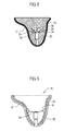
- FIG 1 illustrates a cross sectional view of a housing 10 of a hearing aid device 12 according to an embodiment herein.
- the housing 10 comprises a conductive layer 18 between a first non-conductive layer 14 and a second non-conductive layer 15.
- the conductive layer 18 with the first non-conductive layer 14 and the second non-conductive layer 15 forms the wall of the housing 10.
- the conductive layer 18 provides shielding of an inner space 20 within the housing 10 from electromagnetic interference (EMI).
- EMI electromagnetic interference
- the hearing aid device 12 includes, but not limited to, in-ear hearing aid device, baby worn hearing aid device, behind the ear (BTE) hearing aid device, receiver in the canal (RIC) or ear hearing aid device, in the canal (ITC) hearing aid device, mini canal (MIC) hearing aid device, completely in the canal (CIC) hearing aid device, extended wear hearing aid device, open fit hearing aid devices, eye glass hearing aid devices and the like.
- the first non-conductive layer 14 and the second non-conductive layer 15 are manufactured using non-conductive materials, for example a resin, an adhesive, a paint or a synthetic material, such that the first non-conductive layer 14 and the second non-conductive layer 15 do not exhibit any electrical conductance property.
- the conductive layer 18 is manufactured using conductive materials such that the conductive layer 18 is electrically conductive.
- the conductive layer 18 extends substantially at the interior of the housing 10 between the first non-conductive layer 14 and the second non-conductive layer 15. This provides efficient shielding of the inner space 20.
- the conductive layer 18 can be a thin foil.
- the conductive layer 18 may be embedded between the first conductive layer 14 and the second conductive layer 15 during the manufacturing of the housing 10.
- the housing 10 may be manufactured such that the housing 10 comprises only the conductive layer 18 and the second non-conductive layer 15.
- the housing 10 having the conductive layer 18 between the first non-conductive layer 14 and the second conductive layer 15 shields the inner space 20 from EMI. Providing the conductive layer 18 between the first non-conductive layer 14 and the second non-conductive layer 15 enables efficient usage of the inner space 20 of the housing 10.
- the conductive layer 18 may be provided such that the conductive layer 18 encircles a substantial surface area of the second non-conductive layer 15.
- the conductive layer 18 may be provided such that it encircles only a particular region or portion of interest of the second non-conductive layer 15.
- FIG 2 illustrates a schematic block diagram of electrical components essential for a hearing aid function.
- the hearing aid device 12 comprises therein the electrical components essential for the hearing aid function, such as, a microphone 22, an amplifier 24, a receiver 26 and a power source 28.
- the electrical component may also include resistors, capacitors, coils and the like.
- the electrical components such as the resistor, capacitor or the coil may also be printed using solid freeform fabrication techniques, such as a 3D printing technique.
- the hearing aid device 1 records ambient noise with the aid of the microphone 22, amplifies these by means of the amplifier 24 and forwards them to the receiver 26.
- the power supply required for the amplifier 24 for amplification is provided by the power source 28.
- the sound signals from the receiver 26 are conveyed to the ear drum of the wearer by means of an outlet canal, tube or wire.
- the electrical components are typically arranged in the inner space 20 of the housing 10.
- the conductive layer 18 shields the inner space 20 within the housing 10 from EMI. This shields the electrical components arranged within the inner space 20 from EMI.
- FIG 3 illustrates a cross sectional view of housing 10 comprising an additional conductive layer according to an embodiment herein.
- the housing 10 of the hearing aid device 12 comprises therein the electrical components essential for the functioning of the hearing aid device 12.
- the housing 10 comprises the conductive layer 18 between the first non-conductive layer 14 and the second non-conductive layer 15.
- an additional conductive layer 21 may be attached onto the inner surface 16 of the second non-conductive layer 15 of the housing 10.
- the conductive layer 21 is attached onto the inner surface 16 of the second non-conductive layer 15 of the housing 10 as the second non-conductive layer 15 is manufactured using a non-conductive material.
- the inner surface 16 of the second non-conductive layer 15 acts as a support for the conductive layer 21.
- the additional conductive layer 21 may represent a positive contact or a negative contact.
- multiple conductive layers may be attached onto the inner surface 16 of the second non-conductive layer 15. For example, if two conductive layers are attached the conductive layers may represent a positive and a negative contact. If multiple conductive layers are attached onto the inner surface 16 of the second non-conductive layer 15, the conductive layers would have to be separated using an insulating medium.
- FIG 4a illustrates one example where two conductive layers 21, 30 are separated by an insulating medium 32 to form a positive and a negative contact.
- the insulating medium 32 may be a non-conducting layer of the inner surface 16 of the second non-conductive layer 15 or an insulating layer attached between the conductive layers 21, 30.
- the insulating medium 32 may be an insulating layer such that the insulating layer acts as a barrier between the two additional conductive layers 21, 30 as illustrated in FIG 4b .
- FIG 5 illustrates a pattern of attaching additional conductive layers on the inner surface of second non-conductive layer the housing of the hearing aid device according to an embodiment herein.
- a plurality of additional conductive layers 21, 30 are attached on the inner surface 16 of FIG 3 of the second non-conducive layer 15 of FIG 3 in a stripe pattern.
- one of the additional conductive layers may represent a positive contact and the other may represent a negative contact.
- the additional conductive layers 21 may represent a positive contact and the additional conductive layers 30 may represent a negative contact.
- the additional conductive layers 21 are separated from the additional conductive layers 30 by an insulating medium 32.
- the insulating medium 32 in the present embodiment is portions of the inner surface 16 of the second non-conducive layer 15 onto which no conductive layers 21, 30 are attached.
- FIG 6 illustrates another pattern of attaching additional conductive layers on the inner surface of the housing of the hearing aid device according to an embodiment herein.
- the additional conductive layer 21 is attached on one half of the inner surface 16 of FIG 3 of the second non-conductive layer 15 of FIG 3 and the conductive layer 30 is attached onto the other half of the inner surface 16 of the second non-conductive layer 15.
- the conductive layer 21 is separated from the conductive layer 30 by an insulating medium 32.
- the insulating medium 32 in the present embodiment is portion of the inner surface 16 of the second non-conductive layer 15 onto which no conductive layers 21, 30 are attached.
- Attaching multiple conductive layers enable, conductively connecting multiple conductive layers to the electrical components. This enables in increasing the fault tolerance of the hearing aid device 1 as redundant connections to the electrical components can be made.
- the additional conductive layer 21 extends over a substantial surface area of the inner surface 16 of the second non-conductive layer 15. However, the additional conductive layer 21 may be attached onto only a portion of the inner surface 16 of the second non-conductive layer 21. If the additional conductive layer 21 is attached onto only a portion of the inner surface 16 of the second non-conductive layer 15, it may be required that the additional conductive layer 21 is to be attached onto the inner surface 16 of the second non-conductive layer 15 such that the position of the additional conductive layer 21 is suitable for making connections with electrical components. If a single additional conductive layer is attached onto the inner surface 16 of the second non-conductive layer 15, the additional conductive layer may extend over a substantial area of the inner surface 16 of the second non-conductive layer 15. However, the additional conductive layer can also extend over a portion or region of the surface of the inner surface 16 of the second non-conductive layer 15.
- an electrical component for example a receiver 26 may be connected to the conductive layers 21, 30 using connector leads 34, 36.
- the receiver 24 illustrated in FIG 7 is shown as an example and other electrical components may also be connected in a similar manner.
- Other connector means such as soft rings and the like may also be used to connect an electrical component to the conductive layers 21, 30.
- the connector leads 34, 36 may pierce into the respective conductive layers 21, 30.
- the connector leads 34, 34 enable suspending the receiver 9 rigidly and thus, reduce shocks and vibrations encountered by the receiver due to the movement of the user of the hearing aid device. Additionally, the use of connector leads 34, 36 enable to eliminate the requirement of soldering and thus, make the manufacturing process easy and less time consuming.
- connections from the conductive layers 21, 30 to the electrical component may be made to increase fault tolerance.
- a plurality of connector leads 34, 36 may be used to make the connections between the conductive layers 21, 30 and the electrical component.
- FIG 8 illustrates connection between an electrical component and conductive layers attached onto the inner surface of the housing using connector leads in more detail.
- a receiver 26 is connected to the conductive layers 21, 30 using connector leads 34, 36.
- the connector leads 34, 36 may pierce into the conductive layers 21, 30.
- the connector leads 34, 36 connect to a connection pad and the connection pad in turn connects to the contact terminal of the receiver 26.
- the receiver 26 is held in a suspended position rigidly and thus reduces the chances of device failure due to shock and vibration.
- the multiple connector leads 34, 36 enables in increasing fault tolerance of the hearing aid device 12 of FIG 7 .
- the housing 10 may be manufactured such that connector leads 34, 36 are attached to the housing 10.
- the receiver 26 may be connected to the connector leads 34, 36 and thus connect to the additional conductive layers 21, 30.
- FIG 9 illustrates connection between an electrical component and conductive layers using connection leads attached onto the inner surface of the housing.
- the receiver 26 is connected to the conductive layers 21, 30 using connector leads 34, 36.
- the connector leads 34, 36 are attached to the housing 10 of the hearing aid device 12 and are conductively connected to the conductive layers 21, 30.
- the connector leads 34, 36 may be attached to the housing 10 during fabrication of the housing 12.
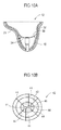
- FIG 10a illustrates connection between an electrical component and conductive layers attached onto the inner surface of the housing of the hearing aid device using soft rings.
- a receiver 26 is connected to the additional conductive layers 21, 30 using soft rings 42.
- FIG 10b illustrates a soft ring 42 in detail.
- the soft ring 42 comprises conductive medium 44 which are connected to the additional conductive layers 21, 30 of FIG 10a .
- the conductive mediums 44 connect to a connection pad 46 on the soft ring 42 and the connection pad 44 connects to the contact terminal of the receiver 26 of FIG 10a .
- the multiple conductive mediums 44 enable multiple connections between the receiver 26 and the conductive layers 21, 30. This increases the fault tolerance of the hearing aid device 12 as redundant connections may be made to an electrical component. In the shown example of FIG 10a , the receiver 26 is held in a suspended position rigidly and thus reduces the chances of device failure due to shock and vibration.
- an amplifier 24 may be connected to the conductive layers 21, 30 using connector leads 38, 40.
- Soft rings 42 of FIG 10a and FIG 10b may also be used to connect the amplifier 24 to the conductive layers 21, 30.
- connecting the receiver 26 and the amplifier 24 to the conductive layers 21, 30 enable conductively connecting the receiver 26 to the amplifier 24 without the requirement of loose wire leads.
- the connector leads 34, 36 hold the receiver 26 in a suspended position which is rigid and reduce shocks and vibrations encountered by the receiver 26 due to the movement of the user of the hearing aid device. Suspending the receiver 26 inside the housing 10 eliminates the need of extra caution to be taken while the hearing aid device is being manufactured. Alternatively, the manufacturing time for the hearing aid device 12 is reduced.
- a face plate 23 is provided at the distal end of the hearing aid device 12.
- the amplifier 24 is mounted onto the face plate 23.
- the face plate 22 and the amplifier 24 may also be printed using the solid freeform techniques.
- the additional conductive layers 21, 30 are attached onto the inner surface 16 of the second non-conductive layer 15 by fabricating the housing 10 and the conductive layers 21, 30. While fabricating the housing 22, the conductive layers 21, 30 may be fabricated onto the inner surface 16 of the second non-conductive layer 15. In certain implementation additional non-conductive layers of the housing 10 may be fabricated onto the inner surface 16 to which the conductive layers 18, 30 are fabricated. Additional non-conductive layers of the housing 10 may be fabricated for fabricating multiple layers of additional conductive layers or for providing insulation as the housing 10 is manufactured using a non-conducting material.
- FIG 11a illustrates separation of a plurality of additional conductive layers using insulating mediums.
- a plurality of additional conductive layers 21a through 21e are separated from each other using insulating mediums 32a through 32f respectively.
- FIG 11b an enlarged side view of the encircled area of FIG 11a is shown.
- the additional conductive layers 21a and 21b are separated by the insulating medium 32a.
- the insulating medium 32a enables to prevent conduction between the additional conductive layers 21a and 21b.
- multiple additional conductive layers may be printed by having respective insulating mediums between them.
- the conductive layers 21a through 21e may be filaments and the point of intersections can be separated by having insulating mediums 32a through 32f therein.
- the electrical components may be fixedly positioned onto the inner surface comprising the conductive layers.
- the conductive layers may be extended onto the outer surface of a casing of the electrical component and thus complete the connection.
- FIG 12a illustrates connection between two electrical components using the additional conductive layers attached onto the inner surface of the second non-conductive layer of the housing of the hearing aid device and extended onto an the outer surface of the casing.
- electrical components for example, a receiver 26 and an amplifier 24 may be held fixedly onto the inner surface 16 of the second non-conductive layer 15.
- the conductive layers 21, 30 may be printed onto the inner surface 16 of the second non-conductive layer 15 and onto the outer surface 48 of the casing 50 of the receiver 26 and the amplifier 24 to connect the receiver 26 and the amplifier 24.
- the additional conductive layers 21, 30 may be conductively connected to a single electrical component to provide power to the electrical component.
- the conductive layers 21, 30 printed onto the outer surface 48 of the casing 50 make contact with connection pads 52 to connect the receiver 26 to the conductive layers 21, 30.
- An insulating medium 32 may be provided between the conductive layers 21, 30 for separating the conductive layers 21, 30.
- the insulating medium 32 is provided at the point of intersection of the conductive layers 21, 30.
- the insulating medium 32 may be provided over the entire surface also.
- the conductive layers 21, 30 are conductive pathways printed onto the inner surface 16 of the second non-conductive layer 15 and the outer surface 48 of the casing 50 of the receiver 26.
- FIG 12b illustrates a side view of the connection between the electrical components using the conductive layers of FIG 12a .
- the conductive layer 21 is illustrated for understanding purposes. It is seen that the conductive layer 21 is printed onto the inner surface 16 and over the outer surface 48 of the casing 50 of the amplifier 24 and the receiver 26.
- the present embodiment provides the advantage of connecting an electrical component to the conductive layers 21, 30 by printing the conductive layers 21, 30 on the outer surface 48 of the casing 50 of the electrical component.
- FIG 13 illustrates connection between an electrical component and a conductive layer using a casing of the electrical component.
- the conductive layer 21 extends over a substantial surface area of the inner surface 16 of the second non-conductive layer 15.
- the conductive layer 21 may extend over only a particular portion or region of the inner surface 16.
- the conductive layer 21 may be adapted to operate either as a positive contact or a negative contact.
- the electrical component for example the receiver 26 comprises a casing 53 having a conductive outer surface 54. The receiver 26 is fixedly positioned onto the conductive layer 21 attached onto the inner surface 16 such that the outer surface 54 of the casing 53 of the receiver 26 is in contact with the conductive layer 21.
- the receiver 26 is shown for the purposes of illustration only and other electrical components may also be positioned onto the conductive layer 21.
- the outer surface 54 of the casing 53 may be connected to a connection point so that the outer surface 54 of the casing 53 is connected to the internal circuitry of the electrical component, i.e., the receiver 26.
- the casing 53 may be made using a conductive material such that the outer surface 54 and an inner surface of the casing 53 are conductive. In an implementation, only a portion of the outer surface 54 of the casing 53 may be conductive.
- the electrical component may be conductively connected to the conductive layer 21. Additionally, one electrical component may be conductively connected to another electrical component using the conductive layer 21.
- the conductive layer 21 may be adapted to operate as a common ground and the outer surface 54 of the casing 53 may be connected to the conductive layer 21 to connect the electrical component to the ground.
- the conductive layer 21 may be adapted to operate as a positive contact and the outer surface 54 of the casing 53 may be connected to the conductive layer 21 to connect the electrical component to a positive contact.
- the housing 22 may comprise a slot to receive an electrical component, for example the receiver 26.
- Fig 14 illustrates a side view of a slot 55 on the inner side 56 of the housing 10.
- the slot 55 is provided on the inner side 56 of the housing 10.
- the electrical component when positioned into the slot 55 is conductively connected to the conductive layer 21.
- the conductive layer 21 may be attached onto a substantial area of the inner surface 16 of the second non-conductive layer 15, including the slot 55. Alternatively, the conductive layer 21 may be attached onto a portion of the inner surface 16 only within the slot 55.
- FIG 15 is a cross sectional view of the housing of the hearing aid device illustrating a coil provided on the first non-conductive layer.
- a coil 58 is provided on the first non-conductive layer 14 of the housing 10.Typicaaly, the coil 58 comprises a structure of a helix and spirals around the non-conductive layer 14 of the housing 10.
- the housing 10 may comprises an additional non-conductive layer 60 over the coil 58.
- the additional non-conductive layer 60 prevents the coil 58 from being damaged and also prevents inconvenience to the user of the hearing aid device 12 due to the presence of the coil 58.
- the coil 58 may be used for wireless communication or for wireless charging of the hearing aid device 12. This enables efficient use of the inner space 20 of FIG 1 of the hearing aid device 12, and thus, enables miniaturization of the hearing aid device 12. Additionally, as the coil 58 is provided external to the first conductive layer 18, the inner space 20 is shielded from any EMI arising out of the coil 58 by the first conductive layer 18.
- the housing 10 of the hearing aid device 12 is manufactured by embedding the first conductive layer 18 between the first non-conductive layer 14 and the second non-conductive layer 15.
- the conductive layer 18 is embedded between the first non-conductive layer 14 and the second non-conductive layer 15 using a solid freeform fabrication technique.
- the solid freeform fabrication technique includes, but not limited to inkjet printing, pneumatic spraying, screen printing, pad printing, laser printing, dot matrix printing, thermal printing, lithography, and 3D printing.
- Solid freeform fabrication technique provides the advantages of enabling the manufacturing of the first conductive layer 18, the first non-conductive layer 14 and the second non-conductive layer 15 simultaneously such that the housing 22 comprises the first conductive layer 18 between the first non-conductive layer 14 and the second non-conductive layer 15. This decreases the manufacturing time of the hearing aid device 1 and also reduces the complexities. Moreover, using solid freeform fabrication technique to manufacture the housing 10 eliminates the requirement for having separate moulds for individual hearing aid device 12 design. However, the housing 10 may be manufactured using other manufacturing techniques such as MID and inset molding. If the hearing aid device is manufactured using a MID or an inset molding technique, a mould may be required to be created for each hearing aid device. Additionally, the manufacturing time of the hearing aid device 12 may be increased as the conductive layer 18, the first non-conductive layer 14 and the second non-conductive layer 15 will have to be manufactured one at a time.
- the housing 10 is fabricated a 3D printing technology.
- Solid freeform fabrication techniques such as the 3D printing technology enables fabricating a product using multiple materials.
- a first printer head may print the first non-conductive layer 14 of the housing
- a second printer head may print the conductive layer 18
- a third printer head may print the second non-conductive layer 15.
- the first printer head may be used to print the second non-conductive layer 15 as typically, the first conductive layer 14 and the second conductive layer 15 comprises the same non-conducting materials.
- the printing is done by fabricating layers one after the next successively in physical space until the model or the product is completed.
- the conductive layer 18, the first conductive layer 18, the first non-conductive layer 14 and the second non-conductive layer 15 may be printed by the respective printer heads by dispersion of suitable respective printing compositions.
- the printing composition for printing the non-conductive layers 14, 15 may comprise particles of non-conducting elements, for example a resin.
- the printing composition for printing the conductive layer 18 may comprise particles of conductive elements, such as copper, gold, silver, electrically conductive polymer, and the like.
- the respective printing compositions for printing the non-conductive layers 14, 15 and the conductive layer 18 may comprise nanoparticles of elements suitable for printing the respective layers.
- the conductive layer 21 may be printed onto the inner surface 16 of the second non-conductive layer 15 in a similar manner. Also the coil 58 and the additional non-conductive layer 60 may be printed in a similar manner.
- Solid freeform fabrication techniques such as the 3D printing technology enables fabricating a product using multiple materials. It will be apparent to a person skilled in the art that the layers of the housing 10 and the conductive layer 18 may be printed simultaneously using freeform fabrication techniques using the respective printing heads such that the end product is the housing 10 having the conductive layer 18 between the first non-conducive layer 14 and the second non-conductive layer 15.
- FIGS 16a through 16c illustrate a method of manufacturing a housing of a hearing aid device according to an embodiment herein.
- a first non-conductive layer 14 of the housing 10 of Fig 1 is printed.
- the first non-conductive layer 14 comprises an inner surface 66 and an outer surface.
- a conductive layer 18 is printed onto the inner surface 66 of the first non-conductive layer 14.
- the conductive layer 18 comprises an inner surface 68.
- a second non-conductive layer 15 is printed onto an inner surface 68 of FIG 16b of the conductive layer 18.
- the conductive layer 18 is positioned between the first non-conductive layer 14 and the second non-conductive layer 15.
- the conductive layer 18 is embedded between the first non-conductive layer 14 and the second non-conductive layer 15 of the housing 10.
- the embodiments described herein provide a shielding layer for shielding the inner space of the hearing aid device from EMI.
- the inner space of the hearing aid device accommodates electrical components essential for the hearing aid function. Moreover, this enables efficient use of the inner space of the housing and thus enables the design of the hearing aid device to me more compact. Additionally, the requirement of loose wire leads to connect electrical components of a hearing aid device may be eliminated. Moreover, the manufacturing time of the hearing aid device is reduced. Eliminating the need of loose wire leads also enables the electronic component to be inserted independently into the housing during manufacturing of the hearing aid device, and thus eliminating the extra caution required during manufacturing. Moreover, certain embodiments provide a means to suspend the receiver rigidly so that the possibility of the failure of the hearing aid device is reduced.
- Suspension of the receiver independently enables the receiver to be pushed into position and thus enable easy repairing of the hearing aid device. Additionally, the elimination of loose wire leads enable in reducing the electromagnetic interference within the hearing aid device. Militarization of the hearing aid device is also possible as the requirement of soldering is eliminated.
Landscapes
- Engineering & Computer Science (AREA)
- Manufacturing & Machinery (AREA)
- Health & Medical Sciences (AREA)
- General Health & Medical Sciences (AREA)
- Neurosurgery (AREA)
- Otolaryngology (AREA)
- Physics & Mathematics (AREA)
- Acoustics & Sound (AREA)
- Signal Processing (AREA)
- Shielding Devices Or Components To Electric Or Magnetic Fields (AREA)
Description
- The present invention relates to a hearing aid device and a method for manufacturing the hearing aid device.
- Hearing aid devices and hearing devices generally comprise a housing, in which a microphone, an amplifier or amplifying device, a receiver, a power supply, mostly a zinc-air battery inter alia are arranged. The receiver is connected to an acoustic output of the housing, which emits the acoustic signals generated and prepared by the hearing aid device into an auditory canal of a wearer of the hearing aid device.
- In order to meet the aesthetic requirements of a wearer of the hearing aid device, this is to be as minimally externally visible on the wearer as possible. These requirements are particularly high especially in the case of hearing devices worn in the ear, referred to as in-ear hearing aid device. The components needed for an in-ear hearing aid device are thus to be designed as small as possible within the in-ear hearing aid device, to be packed as tightly as possible and to be reduced to a minimum.
- Additionally, the components of the hearing aid device are to be shielded from external interferences for efficient functioning of the hearing aid device. Compensating elements such as coils, capacitors or certain topology of conductive lines and cables may be arranged within the inner space of a housing of the hearing aid device to reduce the electromagnetic interferences (EMI) within the housing. Alternatively, a shielding layer, such as having a gold plated layer on the inner surface of the hearing aid device may reduce the EMI within the housing of the hearing aid device. However, the use of compensating elements and the shielding layer may provide limitations on the miniaturization of the hearing aid device. Further, the manufacturing time of the hearing aid device is increased as the compensating elements are to be carefully positioned into the hearing aid device or the gold plated layer is to be provided onto the inner surface of the housing after the after has been made.
-
EP 1465457 discloses a cover for a behind-the-ear hearing aid. The cover includes a shell formed from a rigid material where the shell is adapted for a removable shaped fit over at least a portion of the behind-the-ear hearing aid. Additionally, the cover comprises means to counter the effect of RFI or EMI. -
EP 1317163 discloses a device having a plastic housing of at least two parts containing electronic units or components that are electrically interconnected. At least one housing part and/or at least a plastic component of an electronic unit inside the housing are in the form of a molded part with integrated conducting tracks via which the electronic components or units can be electrically interconnected. -
US 2007/0055147 A1 discloses a medical device, e.g. a pacemaker or a hearing aid, with a conductive layer for shielding the interior of the device against radiation. - It is an object of the invention to provide shielding of components from external electromagnetic interferences.
- The above object is achieved by a hearing aid device and a method of manufacturing the hearing aid device, wherein the hearing aid device comprises a housing having a first non-conductive layer and a second non-conductive layer, and a first conductive layer between the first non-conductive layer and the second non-conductive layer.
- The first conductive layer embedded in between the first non-conducive layer and the second non-conducive layer of the housing of the hearing aid device shields an inner space of the housing from external electromagnetic interferences. The inner space of the housing accommodates the electrical components therein. Further this facilitates further miniaturization of the hearing aid device as the inner space of the housing may be used more efficiently and thus the hearing aid device can be more compact.
- The hearing aid device further comprises a second conductive layer attached onto at least a portion of the inner surface of the second non-conductive layer. The second conductive layer attached onto the inner surface of the second non-conductive layer of the housing of the hearing aid device enables in miniaturization of the hearing aid device. Additionally, the requirement of loose wires leads may be reduced and thus the electromagnetic interference within the housing of the hearing aid device is reduced.
- According to yet another embodiment, the second conductive layer is conductively connected to an electrical component of the hearing aid. Connecting an electrical component to the second conductive layer enables miniaturization of the hearing aid device and eliminates the requirement of loose wire leads.
- According to yet another embodiment, the electrical component includes a printed electrical component. Printed electrical components occupy less space and can easily be printed during the manufacturing of the housing. Thus, printed electrical components enable in miniaturization of the hearing aid device and also reduce the manufacturing time of the hearing aid device.
- According to yet another embodiment, the first conductive layer and the second conductive layer are fabricated using a solid freeform fabrication technique selected from the group consisting of inkjet printing, pneumatic spraying, screen printing, pad printing, laser printing, dot matrix printing, thermal printing, lithography, and 3D printing. Fabricating or printing the first and the second conductive layer using a solid freeform fabrication technique enables in fabricating the first conductive layer between the first non-conducive layer and the second non-conductive layer and the second conductive onto the inner surface of the second non- conductive layer of the housing at the time of the manufacturing of the housing.
- According to yet another embodiment, the first conductive layer and the second conductive layer comprises an element from the group consisting of copper, gold, silver and electrically conductive polymer. These elements comprise enhanced conductive properties and therefore enable the first conductive layer and the second conductive layer to have good electrical conductance.
- The housing further comprises a third non-conductive layer arranged outwardly to the first non-conductive layer. Providing the third non-conductive layer enables providing additional features to the hearing aid device.
- The hearing aid device further comprises a coil between the third non-conductive layer and the first non-conductive layer. The coil enables wireless communication with the hearing aid device. Additionally, the coil enables wireless charging of the hearing aid device. This enables efficient use of the inner space of the hearing aid device, and thus, enables miniaturization of the hearing aid device. Additionally, as the coil is provided external to the first conductive layer, the inner space is shielded from any EMI arising out of the coil by the first conductive layer.
- Another embodiment includes a method of manufacturing a hearing aid device, wherein the method comprises embedding a first conductive layer between a first non-conductive layer and a second non-conductive layer of a housing of the hearing aid device.
- Embedding the first conductive layer between the first non-conductive layer and the second non-conductive layer of the housing provides shielding of the inner space of the housing from EMI interferences. Further this facilitates further miniaturization of the hearing aid device as the inner space of the housing may be used more efficiently and thus the hearing aid device can be more compact.
- The method further comprises attaching a second conductive layer onto an inner surface of the second non-conductive layer. The second conductive layer attached onto the inner surface of the second non-conductive layer of the housing of the hearing aid device enables in miniaturization of the hearing aid device. Additionally, the requirement of loose wires leads may be reduced and thus the electromagnetic interference within the housing of the hearing aid device is reduced.
- According to yet another embodiment, the embedding includes fabricating the first conductive layer between the first non-conductive layer and the second non-conductive layer using a solid freeform technique selected from the group consisting of inkjet printing, pneumatic spraying, screen printing, pad printing, laser printing, dot matrix printing, thermal printing, lithography, and 3D printing.
- According to yet another embodiment, the second conductive layer is conductively connected to an electrical component of the hearing aid.
- According to yet another embodiment, wherein the electrical component includes a printed electrical component.
- The method comprises embedding a coil between the first non-conductive layer and a third non-conductive layer, the third non-conductive layer arranged outwardly to the first non-conductive layer.
- According to yet another embodiment, wherein the first conductive layer, the second conductive layer and the coil comprises an element from the group consisting of copper, silver, gold and electrically conductive polymer.
- The present invention is further described hereinafter with reference to illustrated embodiments shown in the accompanying drawings, in which:
- FIG 1
- illustrates a cross sectional view of a housing of a hearing aid device according to an embodiment herein,
- FIG 2
- illustrates a schematic block diagram of electrical components essential for a hearing aid function,
- FIG 3
- illustrates a cross sectional view of housing comprising an additional conductive layer according to an embodiment herein,
- FIG 4a
- illustrates one example where two conductive layers are separated by an insulating medium to form a positive and a negative contact,
- FIG 4b
- illustrates an insulating medium provided to act as a barrier between two additional conductive layers
- FIG 5
- illustrates a pattern of attaching additional conductive layers on an inner surface of a second non-conductive layer of a housing of a hearing aid device according to an embodiment herein,
- FIG 6
- illustrates another pattern of attaching additional conductive layers on an inner surface of a second non-conductive layer of a housing of a hearing aid device according to an embodiment herein,
- FIG 7
- illustrates connection of an electrical component to the additional conductive layers according to an embodiment herein,
- FIG 8
- illustrates connection between an electrical component and additional conductive layers attached onto an inner surface of a second non-conductive layer in more detail,
- FIG 9
- illustrates connection between an electrical component and additional conductive layers using connection leads attached onto an inner surface of a second non-conductive layer according to an embodiment herein,
- FIG 10a
- illustrates connection between an electrical component and conductive layers attached onto an inner surface of a housing of a hearing aid device using soft rings,
- FIG 10b
- illustrates a soft ring in detail,
- FIG 11a
- illustrates separation of a plurality of conductive layers using insulating mediums in accordance to an embodiment herein,
- FIG 11b
- is an enlarged side view of the encircled area
- of FIG 11a, FIG 12a
- illustrates connection between two electrical components using the additional conductive layers attached onto an inner surface of a second non-conductive layer of a housing of a hearing aid device and extended onto an outer surface of a casing of the electrical components,
- FIG 12b
- additional conductive layers of
FIG 12a , - FIG 13
- illustrates connection between an electrical component and an additional conductive layer using a casing of an electrical component,
- FIG 14
- illustrates a side view of a slot on an inner side of a housing of a hearing aid device according to an embodiment herein,
- FIG 15
- is a cross sectional view of a housing of a hearing aid device illustrating a coil printed onto a layer of the hearing aid device between a first non-conductive layer and a conductive layer according to an embodiment herein, and
- FIGS 16a - 16c
- illustrate a method of manufacturing a housing of a hearing aid device according to an embodiment herein.
- Various embodiments are described with reference to the drawings, wherein like reference numerals are used to refer to like elements throughout. In the following description, for purpose of explanation, numerous specific details are set forth in order to provide a thorough understanding of one or more embodiments. It may be evident that such embodiments may be practiced without these specific details.
-
FIG 1 , illustrates a cross sectional view of ahousing 10 of ahearing aid device 12 according to an embodiment herein. Thehousing 10 comprises aconductive layer 18 between a firstnon-conductive layer 14 and a secondnon-conductive layer 15. Theconductive layer 18 with the firstnon-conductive layer 14 and the secondnon-conductive layer 15 forms the wall of thehousing 10. Theconductive layer 18 provides shielding of aninner space 20 within thehousing 10 from electromagnetic interference (EMI). - The
hearing aid device 12 includes, but not limited to, in-ear hearing aid device, baby worn hearing aid device, behind the ear (BTE) hearing aid device, receiver in the canal (RIC) or ear hearing aid device, in the canal (ITC) hearing aid device, mini canal (MIC) hearing aid device, completely in the canal (CIC) hearing aid device, extended wear hearing aid device, open fit hearing aid devices, eye glass hearing aid devices and the like. - Still referring to
FIG 1 , advantageously, the firstnon-conductive layer 14 and the secondnon-conductive layer 15 are manufactured using non-conductive materials, for example a resin, an adhesive, a paint or a synthetic material, such that the firstnon-conductive layer 14 and the secondnon-conductive layer 15 do not exhibit any electrical conductance property. Theconductive layer 18 is manufactured using conductive materials such that theconductive layer 18 is electrically conductive. - Preferably, the
conductive layer 18 extends substantially at the interior of thehousing 10 between the firstnon-conductive layer 14 and the secondnon-conductive layer 15. This provides efficient shielding of theinner space 20. In an implementation, theconductive layer 18 can be a thin foil. Advantageously, theconductive layer 18 may be embedded between the firstconductive layer 14 and the secondconductive layer 15 during the manufacturing of thehousing 10. Alternatively, thehousing 10 may be manufactured such that thehousing 10 comprises only theconductive layer 18 and the secondnon-conductive layer 15. However, it may not be preferred to manufacture thehousing 10 such that it comprises only theconductive layer 18 and the secondnon-conductive layer 15, as it may cause inconvenience to the user of thehearing aid device 12 because of the hardness of theconductive layer 18. Thehousing 10 having theconductive layer 18 between the firstnon-conductive layer 14 and the secondconductive layer 15 shields theinner space 20 from EMI. Providing theconductive layer 18 between the firstnon-conductive layer 14 and the secondnon-conductive layer 15 enables efficient usage of theinner space 20 of thehousing 10. - Advantageously, the
conductive layer 18 may be provided such that theconductive layer 18 encircles a substantial surface area of the secondnon-conductive layer 15. However, theconductive layer 18 may be provided such that it encircles only a particular region or portion of interest of the secondnon-conductive layer 15. -
FIG 2 illustrates a schematic block diagram of electrical components essential for a hearing aid function. Thehearing aid device 12 comprises therein the electrical components essential for the hearing aid function, such as, amicrophone 22, anamplifier 24, areceiver 26 and apower source 28. The electrical component may also include resistors, capacitors, coils and the like. The electrical components such as the resistor, capacitor or the coil may also be printed using solid freeform fabrication techniques, such as a 3D printing technique. The hearing aid device 1 records ambient noise with the aid of themicrophone 22, amplifies these by means of theamplifier 24 and forwards them to thereceiver 26. The power supply required for theamplifier 24 for amplification is provided by thepower source 28. The sound signals from thereceiver 26 are conveyed to the ear drum of the wearer by means of an outlet canal, tube or wire. - Referring now to
FIG 1 and FIG 2 , the electrical components are typically arranged in theinner space 20 of thehousing 10. In an aspect, theconductive layer 18 shields theinner space 20 within thehousing 10 from EMI. This shields the electrical components arranged within theinner space 20 from EMI. -
FIG 3 illustrates a cross sectional view ofhousing 10 comprising an additional conductive layer according to an embodiment herein. Thehousing 10 of thehearing aid device 12 comprises therein the electrical components essential for the functioning of thehearing aid device 12. In the shown example ofFig 3 , thehousing 10 comprises theconductive layer 18 between the firstnon-conductive layer 14 and the secondnon-conductive layer 15. In an aspect herein, an additionalconductive layer 21 may be attached onto theinner surface 16 of the secondnon-conductive layer 15 of thehousing 10. - The
conductive layer 21 is attached onto theinner surface 16 of the secondnon-conductive layer 15 of thehousing 10 as the secondnon-conductive layer 15 is manufactured using a non-conductive material. Theinner surface 16 of the secondnon-conductive layer 15 acts as a support for theconductive layer 21. - In the shown example of
FIG 3 , the additionalconductive layer 21 may represent a positive contact or a negative contact. However, multiple conductive layers may be attached onto theinner surface 16 of the secondnon-conductive layer 15. For example, if two conductive layers are attached the conductive layers may represent a positive and a negative contact. If multiple conductive layers are attached onto theinner surface 16 of the secondnon-conductive layer 15, the conductive layers would have to be separated using an insulating medium. -
FIG 4a illustrates one example where twoconductive layers medium 32 to form a positive and a negative contact. The insulatingmedium 32 may be a non-conducting layer of theinner surface 16 of the secondnon-conductive layer 15 or an insulating layer attached between theconductive layers medium 32 may be an insulating layer such that the insulating layer acts as a barrier between the two additionalconductive layers FIG 4b . -
FIG 5 illustrates a pattern of attaching additional conductive layers on the inner surface of second non-conductive layer the housing of the hearing aid device according to an embodiment herein. In the shown example ofFIG 5 , a plurality of additionalconductive layers inner surface 16 ofFIG 3 of the secondnon-conducive layer 15 ofFIG 3 in a stripe pattern. For example, one of the additional conductive layers may represent a positive contact and the other may represent a negative contact. For example, the additionalconductive layers 21 may represent a positive contact and the additionalconductive layers 30 may represent a negative contact. The additionalconductive layers 21 are separated from the additionalconductive layers 30 by an insulatingmedium 32. The insulatingmedium 32 in the present embodiment is portions of theinner surface 16 of the secondnon-conducive layer 15 onto which noconductive layers -
FIG 6 illustrates another pattern of attaching additional conductive layers on the inner surface of the housing of the hearing aid device according to an embodiment herein. In the shown example ofFIG 5 , the additionalconductive layer 21 is attached on one half of theinner surface 16 ofFIG 3 of the secondnon-conductive layer 15 ofFIG 3 and theconductive layer 30 is attached onto the other half of theinner surface 16 of the secondnon-conductive layer 15. Theconductive layer 21 is separated from theconductive layer 30 by an insulatingmedium 32. The insulatingmedium 32 in the present embodiment is portion of theinner surface 16 of the secondnon-conductive layer 15 onto which noconductive layers - Attaching multiple conductive layers enable, conductively connecting multiple conductive layers to the electrical components. This enables in increasing the fault tolerance of the hearing aid device 1 as redundant connections to the electrical components can be made.
- In the shown example of
FIG 3 , the additionalconductive layer 21 extends over a substantial surface area of theinner surface 16 of the secondnon-conductive layer 15. However, the additionalconductive layer 21 may be attached onto only a portion of theinner surface 16 of the secondnon-conductive layer 21. If the additionalconductive layer 21 is attached onto only a portion of theinner surface 16 of the secondnon-conductive layer 15, it may be required that the additionalconductive layer 21 is to be attached onto theinner surface 16 of the secondnon-conductive layer 15 such that the position of the additionalconductive layer 21 is suitable for making connections with electrical components. If a single additional conductive layer is attached onto theinner surface 16 of the secondnon-conductive layer 15, the additional conductive layer may extend over a substantial area of theinner surface 16 of the secondnon-conductive layer 15. However, the additional conductive layer can also extend over a portion or region of the surface of theinner surface 16 of the secondnon-conductive layer 15. - Referring now to
FIG 7 , an electrical component, for example areceiver 26 may be connected to theconductive layers receiver 24 illustrated inFIG 7 is shown as an example and other electrical components may also be connected in a similar manner. Other connector means, such as soft rings and the like may also be used to connect an electrical component to theconductive layers conductive layers - In an embodiment, multiple connections from the
conductive layers conductive layers -
FIG 8 illustrates connection between an electrical component and conductive layers attached onto the inner surface of the housing using connector leads in more detail. In the shown example ofFIG 8 , areceiver 26 is connected to theconductive layers conductive layers receiver 26. In the shown example ofFIG 6 , thereceiver 26 is held in a suspended position rigidly and thus reduces the chances of device failure due to shock and vibration. The multiple connector leads 34, 36 enables in increasing fault tolerance of thehearing aid device 12 ofFIG 7 . - Referring again to
FIG 7 , in an alternative implementation, thehousing 10 may be manufactured such that connector leads 34, 36 are attached to thehousing 10. Thereceiver 26 may be connected to the connector leads 34, 36 and thus connect to the additionalconductive layers FIG 9 illustrates connection between an electrical component and conductive layers using connection leads attached onto the inner surface of the housing. Thereceiver 26 is connected to theconductive layers housing 10 of thehearing aid device 12 and are conductively connected to theconductive layers housing 10 during fabrication of thehousing 12. - Referring now to
FIG 7 andFIGS 10a through 10b , in another implementationsoft ring 42 may be used to connect thereceiver 26 to theconductive layers receiver 26 rigidly.FIG 10a illustrates connection between an electrical component and conductive layers attached onto the inner surface of the housing of the hearing aid device using soft rings. In the shown example ofFIG 10a , areceiver 26 is connected to the additionalconductive layers soft rings 42.FIG 10b illustrates asoft ring 42 in detail. Thesoft ring 42 comprises conductive medium 44 which are connected to the additionalconductive layers FIG 10a . Theconductive mediums 44 connect to aconnection pad 46 on thesoft ring 42 and theconnection pad 44 connects to the contact terminal of thereceiver 26 ofFIG 10a . The multipleconductive mediums 44 enable multiple connections between thereceiver 26 and theconductive layers hearing aid device 12 as redundant connections may be made to an electrical component. In the shown example ofFIG 10a , thereceiver 26 is held in a suspended position rigidly and thus reduces the chances of device failure due to shock and vibration. - Referring again to
FIG 7 , another electrical component, for example, anamplifier 24 may be connected to theconductive layers FIG 10a and FIG 10b may also be used to connect theamplifier 24 to theconductive layers receiver 26 and theamplifier 24 to theconductive layers receiver 26 to theamplifier 24 without the requirement of loose wire leads. Moreover, the connector leads 34, 36 hold thereceiver 26 in a suspended position which is rigid and reduce shocks and vibrations encountered by thereceiver 26 due to the movement of the user of the hearing aid device. Suspending thereceiver 26 inside thehousing 10 eliminates the need of extra caution to be taken while the hearing aid device is being manufactured. Alternatively, the manufacturing time for thehearing aid device 12 is reduced. - In an embodiment, a
face plate 23 is provided at the distal end of thehearing aid device 12. Typically, theamplifier 24 is mounted onto theface plate 23. In an implementation, theface plate 22 and theamplifier 24 may also be printed using the solid freeform techniques. - Still referring to
Fig 7 , preferably, the additionalconductive layers inner surface 16 of the secondnon-conductive layer 15 by fabricating thehousing 10 and theconductive layers housing 22, theconductive layers inner surface 16 of the secondnon-conductive layer 15. In certain implementation additional non-conductive layers of thehousing 10 may be fabricated onto theinner surface 16 to which theconductive layers housing 10 may be fabricated for fabricating multiple layers of additional conductive layers or for providing insulation as thehousing 10 is manufactured using a non-conducting material. - Multiple additional conductive layers one above the other may also be provided. Advantageously, one additional conductive layer may be separated from another by an insulating medium. Alternatively an insulating layer may be attached onto the
inner surface 16 of the secondnon-conductive layer 15 to separate two additional conductive layers. In an example, if the additional conductive layers are conductive pathways, the point of intersection of two additional conductive layers may be separated by having an insulating layer therein.FIG 11a illustrates separation of a plurality of additional conductive layers using insulating mediums. A plurality of additionalconductive layers 21a through 21e are separated from each other usinginsulating mediums 32a through 32f respectively. In the example ofFIG 11b , an enlarged side view of the encircled area ofFIG 11a is shown. It is seen that the additionalconductive layers medium 32a. The insulatingmedium 32a enables to prevent conduction between the additionalconductive layers - Referring now to
FIG 11a and FIG 11b , in an implementation theconductive layers 21a through 21e may be filaments and the point of intersections can be separated by having insulatingmediums 32a through 32f therein. - In another embodiment, the electrical components may be fixedly positioned onto the inner surface comprising the conductive layers. The conductive layers may be extended onto the outer surface of a casing of the electrical component and thus complete the connection.
FIG 12a illustrates connection between two electrical components using the additional conductive layers attached onto the inner surface of the second non-conductive layer of the housing of the hearing aid device and extended onto an the outer surface of the casing. In the shown example ofFIG 12a , electrical components, for example, areceiver 26 and anamplifier 24 may be held fixedly onto theinner surface 16 of the secondnon-conductive layer 15. Theconductive layers inner surface 16 of the secondnon-conductive layer 15 and onto theouter surface 48 of thecasing 50 of thereceiver 26 and theamplifier 24 to connect thereceiver 26 and theamplifier 24. Alternatively, the additionalconductive layers conductive layers outer surface 48 of thecasing 50 make contact withconnection pads 52 to connect thereceiver 26 to theconductive layers medium 32 may be provided between theconductive layers conductive layers medium 32 is provided at the point of intersection of theconductive layers medium 32 may be provided over the entire surface also. Preferably, in the present embodiment, theconductive layers inner surface 16 of the secondnon-conductive layer 15 and theouter surface 48 of thecasing 50 of thereceiver 26. -
FIG 12b illustrates a side view of the connection between the electrical components using the conductive layers ofFIG 12a . In the example ofFIG 12b , only theconductive layer 21 is illustrated for understanding purposes. It is seen that theconductive layer 21 is printed onto theinner surface 16 and over theouter surface 48 of thecasing 50 of theamplifier 24 and thereceiver 26. The present embodiment provides the advantage of connecting an electrical component to theconductive layers conductive layers outer surface 48 of thecasing 50 of the electrical component. -
FIG 13 illustrates connection between an electrical component and a conductive layer using a casing of the electrical component. Preferably, theconductive layer 21 extends over a substantial surface area of theinner surface 16 of the secondnon-conductive layer 15. However, theconductive layer 21 may extend over only a particular portion or region of theinner surface 16. In the present example, theconductive layer 21 may be adapted to operate either as a positive contact or a negative contact. The electrical component, for example thereceiver 26 comprises acasing 53 having a conductiveouter surface 54. Thereceiver 26 is fixedly positioned onto theconductive layer 21 attached onto theinner surface 16 such that theouter surface 54 of thecasing 53 of thereceiver 26 is in contact with theconductive layer 21. Thereceiver 26 is shown for the purposes of illustration only and other electrical components may also be positioned onto theconductive layer 21. Internally, theouter surface 54 of thecasing 53 may be connected to a connection point so that theouter surface 54 of thecasing 53 is connected to the internal circuitry of the electrical component, i.e., thereceiver 26. In an alternative embodiment, thecasing 53 may be made using a conductive material such that theouter surface 54 and an inner surface of thecasing 53 are conductive. In an implementation, only a portion of theouter surface 54 of thecasing 53 may be conductive. If only a portion of theouter surface 54 of thecasing 53 is conductive, it may be required that thereceiver 26 be positioned onto theconductive layer 21 such that the conductive portion of theouter surface 54 of thecasing 53 in is contact with theconductive layer 21. Accordingly, the electrical component may be conductively connected to theconductive layer 21. Additionally, one electrical component may be conductively connected to another electrical component using theconductive layer 21. - For an example, the
conductive layer 21 may be adapted to operate as a common ground and theouter surface 54 of thecasing 53 may be connected to theconductive layer 21 to connect the electrical component to the ground. Alternatively, theconductive layer 21 may be adapted to operate as a positive contact and theouter surface 54 of thecasing 53 may be connected to theconductive layer 21 to connect the electrical component to a positive contact. - In an embodiment, the
housing 22 may comprise a slot to receive an electrical component, for example thereceiver 26.Fig 14 illustrates a side view of aslot 55 on theinner side 56 of thehousing 10. Theslot 55 is provided on theinner side 56 of thehousing 10. The electrical component when positioned into theslot 55 is conductively connected to theconductive layer 21. Theconductive layer 21 may be attached onto a substantial area of theinner surface 16 of the secondnon-conductive layer 15, including theslot 55. Alternatively, theconductive layer 21 may be attached onto a portion of theinner surface 16 only within theslot 55. - This enables in reducing the requirement of loose wire leads and thus reduces the electromagnetic interference within the hearing aid device. Additionally, as there is no requirement of soldering, the manufacturing time is reduced and also there is possibility of miniaturizing the hearing aid device as the area covered by a soldering point is substantially large.
-
FIG 15 is a cross sectional view of the housing of the hearing aid device illustrating a coil provided on the first non-conductive layer. In the shown example ofFig 15 , acoil 58 is provided on the firstnon-conductive layer 14 of the housing 10.Typicaaly, thecoil 58 comprises a structure of a helix and spirals around thenon-conductive layer 14 of thehousing 10. Thehousing 10 may comprises an additionalnon-conductive layer 60 over thecoil 58. The additionalnon-conductive layer 60 prevents thecoil 58 from being damaged and also prevents inconvenience to the user of thehearing aid device 12 due to the presence of thecoil 58. - The
coil 58 may be used for wireless communication or for wireless charging of thehearing aid device 12. This enables efficient use of theinner space 20 ofFIG 1 of thehearing aid device 12, and thus, enables miniaturization of thehearing aid device 12. Additionally, as thecoil 58 is provided external to the firstconductive layer 18, theinner space 20 is shielded from any EMI arising out of thecoil 58 by the firstconductive layer 18. - Referring now to
FIG 1 through FIG 15 , thehousing 10 of thehearing aid device 12 is manufactured by embedding the firstconductive layer 18 between the firstnon-conductive layer 14 and the secondnon-conductive layer 15. Advantageously, theconductive layer 18 is embedded between the firstnon-conductive layer 14 and the secondnon-conductive layer 15 using a solid freeform fabrication technique. The solid freeform fabrication technique includes, but not limited to inkjet printing, pneumatic spraying, screen printing, pad printing, laser printing, dot matrix printing, thermal printing, lithography, and 3D printing. Solid freeform fabrication technique provides the advantages of enabling the manufacturing of the firstconductive layer 18, the firstnon-conductive layer 14 and the secondnon-conductive layer 15 simultaneously such that thehousing 22 comprises the firstconductive layer 18 between the firstnon-conductive layer 14 and the secondnon-conductive layer 15. This decreases the manufacturing time of the hearing aid device 1 and also reduces the complexities. Moreover, using solid freeform fabrication technique to manufacture thehousing 10 eliminates the requirement for having separate moulds for individualhearing aid device 12 design. However, thehousing 10 may be manufactured using other manufacturing techniques such as MID and inset molding. If the hearing aid device is manufactured using a MID or an inset molding technique, a mould may be required to be created for each hearing aid device. Additionally, the manufacturing time of thehearing aid device 12 may be increased as theconductive layer 18, the firstnon-conductive layer 14 and the secondnon-conductive layer 15 will have to be manufactured one at a time. - In a preferred embodiment, the
housing 10 is fabricated a 3D printing technology. Solid freeform fabrication techniques, such as the 3D printing technology enables fabricating a product using multiple materials. For example, a first printer head may print the firstnon-conductive layer 14 of the housing, a second printer head may print theconductive layer 18 and a third printer head may print the secondnon-conductive layer 15. The first printer head may be used to print the secondnon-conductive layer 15 as typically, the firstconductive layer 14 and the secondconductive layer 15 comprises the same non-conducting materials. The printing is done by fabricating layers one after the next successively in physical space until the model or the product is completed. - For example, the
conductive layer 18, the firstconductive layer 18, the firstnon-conductive layer 14 and the secondnon-conductive layer 15 may be printed by the respective printer heads by dispersion of suitable respective printing compositions. The printing composition for printing thenon-conductive layers conductive layer 18 may comprise particles of conductive elements, such as copper, gold, silver, electrically conductive polymer, and the like. The respective printing compositions for printing thenon-conductive layers conductive layer 18 may comprise nanoparticles of elements suitable for printing the respective layers. Theconductive layer 21 may be printed onto theinner surface 16 of the secondnon-conductive layer 15 in a similar manner. Also thecoil 58 and the additionalnon-conductive layer 60 may be printed in a similar manner. - Solid freeform fabrication techniques, such as the 3D printing technology enables fabricating a product using multiple materials. It will be apparent to a person skilled in the art that the layers of the
housing 10 and theconductive layer 18 may be printed simultaneously using freeform fabrication techniques using the respective printing heads such that the end product is thehousing 10 having theconductive layer 18 between the firstnon-conducive layer 14 and the secondnon-conductive layer 15. -
FIGS 16a through 16c illustrate a method of manufacturing a housing of a hearing aid device according to an embodiment herein. Referring now toFIG 16a a firstnon-conductive layer 14 of thehousing 10 ofFig 1 is printed. The firstnon-conductive layer 14 comprises an inner surface 66 and an outer surface. Next, as illustrated inFIG 16b , aconductive layer 18 is printed onto the inner surface 66 of the firstnon-conductive layer 14. Theconductive layer 18 comprises aninner surface 68. InFIG 16c , a secondnon-conductive layer 15 is printed onto aninner surface 68 ofFIG 16b of theconductive layer 18. Thus theconductive layer 18 is positioned between the firstnon-conductive layer 14 and the secondnon-conductive layer 15. - Thus, the
conductive layer 18 is embedded between the firstnon-conductive layer 14 and the secondnon-conductive layer 15 of thehousing 10. - The embodiments described herein provide a shielding layer for shielding the inner space of the hearing aid device from EMI. The inner space of the hearing aid device accommodates electrical components essential for the hearing aid function. Moreover, this enables efficient use of the inner space of the housing and thus enables the design of the hearing aid device to me more compact. Additionally, the requirement of loose wire leads to connect electrical components of a hearing aid device may be eliminated. Moreover, the manufacturing time of the hearing aid device is reduced. Eliminating the need of loose wire leads also enables the electronic component to be inserted independently into the housing during manufacturing of the hearing aid device, and thus eliminating the extra caution required during manufacturing. Moreover, certain embodiments provide a means to suspend the receiver rigidly so that the possibility of the failure of the hearing aid device is reduced. Suspension of the receiver independently enables the receiver to be pushed into position and thus enable easy repairing of the hearing aid device. Additionally, the elimination of loose wire leads enable in reducing the electromagnetic interference within the hearing aid device. Militarization of the hearing aid device is also possible as the requirement of soldering is eliminated.
- While this invention has been described in detail with reference to certain preferred embodiments, it should be appreciated that the present invention is not limited to those precise embodiments. Rather, in view of the present disclosure which describes the current best mode for practicing the invention, many modifications and variations would present themselves, to those of skill in the art without departing from the scope and spirit of this invention. The scope of the invention is, therefore, indicated by the following claims rather than by the foregoing description. All changes, modifications, and variations coming within the meaning and range of equivalency of the claims are to be considered within their scope.
Claims (10)
- A hearing aid device, comprising:a housing comprising a first non-conductive layer and a second non-conductive layer; anda first conductive layer between the first non-conductive layer and the second non-conductive layer,wherein the first conductive layer embedded in between the first non-conducive layer and the second non-conducive layer of the housing of the hearing aid device shields an inner space of the housing from external electromagnetic interferences,whereina second conductive layer is attached onto a portion of an inner surface of the second non-conductive layer characterized inthe housing further comprising a third non-conductive layer arranged outwardly to the first non-conductive layer, further comprising a coil between the third non-conductive layer andthe first non-conductive layer.
- The hearing aid device as claimed in claim 1, wherein the second conductive layer is conductively connected to an electrical component of the hearing aid device.
- The hearing aid device as claimed in claim 2, wherein the electrical component comprises a printed electrical component.
- The hearing aid device as claimed in claim 1, wherein the first conductive layer and the second conductive layer are fabricated using a solid freeform fabrication technique selected from the group consisting of: a inkjet printing, a pneumatic spraying, a screen printing, a pad printing, a laser printing, a dot matrix printing, a thermal printing, a lithography, and a 3D printing.
- The hearing aid device as claimed in claim 1, wherein the first conductive layer and the second conductive layer comprises an element selected from the group consisting of: a copper, a gold, a silver, and an electrically conductive polymer.
- A method for manufacturing a hearing aid device, comprising:producing a housing of the hearing aid device comprising a first non-conductive layer and a second non-conductive layer;andembedding a first conductive layer between the first non-conductive layer and the second non-conductive layer,wherein the first conductive layer embedded in between the first non-conducive layer and the second non-conducive layer of the housing of the hearing aid device shields an inner space of the housing from external electromagnetic interferences,attaching a second conductive layer onto an inner surface of the second non-conductive layercharacterized infurther comprising embedding a coil between the first non-conductive layer and a third non-conductive layer, whereinthe third non-conductive layer is arranged outwardly to the first non-conductive layer.
- The method as claimed in claim 6, wherein the first conductive layer is embedded between the first non-conductive layer and the second non-conductive layer by a solid freeform technique selected from the group consisting of: a inkjet printing, a pneumatic spraying, a screen printing, a pad printing, a laser printing, a dot matrix printing, a thermal printing, a lithography, and a 3D printing.
- The method as claimed in claim 6, further comprising conductively connecting an electrical component of the hearing aid device to the second conductive layer.
- The method as claimed in claim 8, wherein the electrical component comprises a printed electrical component.
- The method as claimed in claim 6, wherein the first conductive layer, the second conductive layer, and the coil comprises an element selected from the group consisting of: a copper, a gold, a silver, and an electrically conductive polymer.
Applications Claiming Priority (2)
| Application Number | Priority Date | Filing Date | Title |
|---|---|---|---|
| US12/549,450 US8224006B2 (en) | 2009-08-28 | 2009-08-28 | Hearing aid device and a method of manufacturing a hearing aid device |
| PCT/US2010/046485 WO2011025780A1 (en) | 2009-08-28 | 2010-08-24 | Hearing aid device and a method of manufacturing a hearing aid device |
Publications (2)
| Publication Number | Publication Date |
|---|---|
| EP2471278A1 EP2471278A1 (en) | 2012-07-04 |
| EP2471278B1 true EP2471278B1 (en) | 2015-07-08 |
Family
ID=42990165
Family Applications (1)
| Application Number | Title | Priority Date | Filing Date |
|---|---|---|---|
| EP10748036.0A Active EP2471278B1 (en) | 2009-08-28 | 2010-08-24 | Hearing aid device and a method of manufacturing a hearing aid device |
Country Status (4)
| Country | Link |
|---|---|
| US (2) | US8224006B2 (en) |
| EP (1) | EP2471278B1 (en) |
| DK (1) | DK2471278T3 (en) |
| WO (1) | WO2011025780A1 (en) |
Families Citing this family (14)
| Publication number | Priority date | Publication date | Assignee | Title |
|---|---|---|---|---|
| US8041066B2 (en) | 2007-01-03 | 2011-10-18 | Starkey Laboratories, Inc. | Wireless system for hearing communication devices providing wireless stereo reception modes |
| US9774961B2 (en) | 2005-06-05 | 2017-09-26 | Starkey Laboratories, Inc. | Hearing assistance device ear-to-ear communication using an intermediate device |
| US8208642B2 (en) | 2006-07-10 | 2012-06-26 | Starkey Laboratories, Inc. | Method and apparatus for a binaural hearing assistance system using monaural audio signals |
| US9420385B2 (en) | 2009-12-21 | 2016-08-16 | Starkey Laboratories, Inc. | Low power intermittent messaging for hearing assistance devices |
| US9374650B2 (en) * | 2012-07-17 | 2016-06-21 | Starkey Laboratories, Inc. | System and method for embedding conductive traces into hearing assistance device housings |
| US20140079281A1 (en) * | 2012-09-17 | 2014-03-20 | Gravity Jack, Inc. | Augmented reality creation and consumption |
| US9101046B2 (en) | 2013-01-29 | 2015-08-04 | Mediguide Ltd. | Shielded twisted pair of conductors using conductive ink |
| AU2014302635B8 (en) | 2013-06-24 | 2018-12-06 | President And Fellows Of Harvard College | Printed three-dimensional (3D) functional part and method of making |
| US9545302B2 (en) | 2013-11-20 | 2017-01-17 | Dermagenesis Llc | Skin printing and auto-grafting |
| DE102014216086A1 (en) * | 2014-08-13 | 2016-02-18 | Sivantos Pte. Ltd. | Device and method for integrating hearing device components |
| US10257624B2 (en) * | 2015-08-17 | 2019-04-09 | Starkey Laboratories, Inc. | Hearing aid wireless antenna molded into the device shell |
| EP3520439B1 (en) * | 2016-09-29 | 2022-03-16 | Sonova AG | A hearing device and a method for manufacturing thereof |
| US10085097B2 (en) * | 2016-10-04 | 2018-09-25 | Starkey Laboratories, Inc. | Hearing assistance device incorporating system in package module |
| EP3860153B1 (en) | 2020-01-31 | 2025-07-02 | Oticon A/s | Hearing aid including induction coil |
Citations (2)
| Publication number | Priority date | Publication date | Assignee | Title |
|---|---|---|---|---|
| US6532295B1 (en) * | 1999-12-10 | 2003-03-11 | Sonic Innovations, Inc. | Method for fitting a universal hearing device shell and conformal tip in an ear canal |
| US20070055147A1 (en) * | 2005-09-06 | 2007-03-08 | Honeywell International Inc. | Medical devices incorporating radio-opaque and biocompatible coatings |
Family Cites Families (10)
| Publication number | Priority date | Publication date | Assignee | Title |
|---|---|---|---|---|
| DE3639402A1 (en) | 1986-11-18 | 1988-05-19 | Siemens Ag | METHOD FOR THE PRODUCTION OF A MULTI-LAYERED CIRCUIT BOARD AND THE CIRCUIT BOARD PRODUCED THEREOF |
| US6546109B1 (en) * | 2000-01-03 | 2003-04-08 | Louis Thomas Gnecco | Electromagnetically shielded hearing aids |
| JP2002534933A (en) * | 1999-01-07 | 2002-10-15 | サーノフ コーポレイション | Hearing aid with large diaphragm microphone element with printed circuit board |
| US6768654B2 (en) * | 2000-09-18 | 2004-07-27 | Wavezero, Inc. | Multi-layered structures and methods for manufacturing the multi-layered structures |
| DE10214542C1 (en) | 2002-04-02 | 2003-11-13 | Siemens Audiologische Technik | Contact device for hearing aids |
| EP1317163B1 (en) | 2002-10-22 | 2012-08-29 | Phonak Ag | Hearing aid |
| US20040196996A1 (en) | 2003-04-02 | 2004-10-07 | Feitel Mark A. | Hearing aid and hearing aid accessory cosmetic and functional cover |
| DE102005046169A1 (en) * | 2005-09-27 | 2007-04-05 | Siemens Audiologische Technik Gmbh | Hearing aid with an antenna |
| US8563348B2 (en) | 2007-04-18 | 2013-10-22 | Nanoco Technologies Ltd. | Fabrication of electrically active films based on multiple layers |
| DE102007042590A1 (en) | 2007-09-07 | 2009-03-26 | Siemens Medical Instruments Pte. Ltd. | Hearing aid device, particularly behind ear hearing aid device, has electromagnetic shielding or electromagnetic shielding component, in which component comprises electromagnetic shielding layer materially connected with component |
-
2009
- 2009-08-28 US US12/549,450 patent/US8224006B2/en active Active
-
2010
- 2010-08-24 WO PCT/US2010/046485 patent/WO2011025780A1/en not_active Ceased
- 2010-08-24 DK DK10748036.0T patent/DK2471278T3/en active
- 2010-08-24 US US13/393,005 patent/US9271095B2/en active Active
- 2010-08-24 EP EP10748036.0A patent/EP2471278B1/en active Active
Patent Citations (2)
| Publication number | Priority date | Publication date | Assignee | Title |
|---|---|---|---|---|
| US6532295B1 (en) * | 1999-12-10 | 2003-03-11 | Sonic Innovations, Inc. | Method for fitting a universal hearing device shell and conformal tip in an ear canal |
| US20070055147A1 (en) * | 2005-09-06 | 2007-03-08 | Honeywell International Inc. | Medical devices incorporating radio-opaque and biocompatible coatings |
Also Published As
| Publication number | Publication date |
|---|---|
| DK2471278T3 (en) | 2015-10-12 |
| US8224006B2 (en) | 2012-07-17 |
| WO2011025780A1 (en) | 2011-03-03 |
| US20120250920A1 (en) | 2012-10-04 |
| EP2471278A1 (en) | 2012-07-04 |
| US9271095B2 (en) | 2016-02-23 |
| US20110051965A1 (en) | 2011-03-03 |
Similar Documents
| Publication | Publication Date | Title |
|---|---|---|
| US8224006B2 (en) | Hearing aid device and a method of manufacturing a hearing aid device | |
| US8254608B2 (en) | Hearing aid device and method of producing a hearing aid device | |
| US11483667B2 (en) | Hearing device including an external antenna part and an internal antenna part | |
| EP3103511B1 (en) | Cochlear hearing device with cable antenna | |
| EP3343955B1 (en) | Assembly for hearing aid | |
| US10966036B2 (en) | Hearing device including an external antenna and an internal parasitic element | |
| US10555098B2 (en) | Hearing device including an external antenna part and an internal antenna part | |
| US20150023539A1 (en) | System and method for embedding conductive traces into hearing assistance device housings | |
| US9668067B2 (en) | Hearing device with improved low frequency response and method for manufacturing such a hearing device | |
| US20120155684A1 (en) | Hearing Aid Device and Method of Producing a Hearing Aid Device | |
| EP3591996B1 (en) | A hearing device including an external antenna part and an internal antenna part | |
| US20180317032A1 (en) | Method for producing a supporting frame of a hearing aid, supporting frame and hearing aid |
Legal Events
| Date | Code | Title | Description |
|---|---|---|---|
| PUAI | Public reference made under article 153(3) epc to a published international application that has entered the european phase |
Free format text: ORIGINAL CODE: 0009012 |
|
| 17P | Request for examination filed |
Effective date: 20120216 |
|
| AK | Designated contracting states |
Kind code of ref document: A1 Designated state(s): AL AT BE BG CH CY CZ DE DK EE ES FI FR GB GR HR HU IE IS IT LI LT LU LV MC MK MT NL NO PL PT RO SE SI SK SM TR |
|
| DAX | Request for extension of the european patent (deleted) | ||
| 17Q | First examination report despatched |
Effective date: 20130318 |
|
| GRAP | Despatch of communication of intention to grant a patent |
Free format text: ORIGINAL CODE: EPIDOSNIGR1 |
|
| INTG | Intention to grant announced |
Effective date: 20150211 |
|
| GRAS | Grant fee paid |
Free format text: ORIGINAL CODE: EPIDOSNIGR3 |
|
| GRAA | (expected) grant |
Free format text: ORIGINAL CODE: 0009210 |
|
| AK | Designated contracting states |
Kind code of ref document: B1 Designated state(s): AL AT BE BG CH CY CZ DE DK EE ES FI FR GB GR HR HU IE IS IT LI LT LU LV MC MK MT NL NO PL PT RO SE SI SK SM TR |
|
| REG | Reference to a national code |
Ref country code: GB Ref legal event code: FG4D |
|
| REG | Reference to a national code |
Ref country code: AT Ref legal event code: REF Ref document number: 736186 Country of ref document: AT Kind code of ref document: T Effective date: 20150715 Ref country code: CH Ref legal event code: EP |
|
| REG | Reference to a national code |
Ref country code: IE Ref legal event code: FG4D |
|
| REG | Reference to a national code |
Ref country code: DE Ref legal event code: R096 Ref document number: 602010025749 Country of ref document: DE |
|
| REG | Reference to a national code |
Ref country code: CH Ref legal event code: NV Representative=s name: E. BLUM AND CO. AG PATENT- UND MARKENANWAELTE , CH Ref country code: CH Ref legal event code: PFA Owner name: SIVANTOS PTE. LTD., SG Free format text: FORMER OWNER: SIEMENS MEDICAL INSTRUMENTS PTE. LTD., SG |
|
| REG | Reference to a national code |
Ref country code: DK Ref legal event code: T3 Effective date: 20151009 |
|
| REG | Reference to a national code |
Ref country code: CH Ref legal event code: PCOW Free format text: NEW ADDRESS: 28 AYER RAJAH CRESCENT 06-08, SINGAPORE 139959 (SG) |
|
| RAP2 | Party data changed (patent owner data changed or rights of a patent transferred) |
Owner name: SIVANTOS PTE. LTD. |
|
| REG | Reference to a national code |
Ref country code: AT Ref legal event code: MK05 Ref document number: 736186 Country of ref document: AT Kind code of ref document: T Effective date: 20150708 |
|
| REG | Reference to a national code |
Ref country code: NL Ref legal event code: MP Effective date: 20150708 |
|
| REG | Reference to a national code |
Ref country code: LT Ref legal event code: MG4D |
|
| PG25 | Lapsed in a contracting state [announced via postgrant information from national office to epo] |
Ref country code: FI Free format text: LAPSE BECAUSE OF FAILURE TO SUBMIT A TRANSLATION OF THE DESCRIPTION OR TO PAY THE FEE WITHIN THE PRESCRIBED TIME-LIMIT Effective date: 20150708 Ref country code: NO Free format text: LAPSE BECAUSE OF FAILURE TO SUBMIT A TRANSLATION OF THE DESCRIPTION OR TO PAY THE FEE WITHIN THE PRESCRIBED TIME-LIMIT Effective date: 20151008 Ref country code: LV Free format text: LAPSE BECAUSE OF FAILURE TO SUBMIT A TRANSLATION OF THE DESCRIPTION OR TO PAY THE FEE WITHIN THE PRESCRIBED TIME-LIMIT Effective date: 20150708 Ref country code: LT Free format text: LAPSE BECAUSE OF FAILURE TO SUBMIT A TRANSLATION OF THE DESCRIPTION OR TO PAY THE FEE WITHIN THE PRESCRIBED TIME-LIMIT Effective date: 20150708 Ref country code: GR Free format text: LAPSE BECAUSE OF FAILURE TO SUBMIT A TRANSLATION OF THE DESCRIPTION OR TO PAY THE FEE WITHIN THE PRESCRIBED TIME-LIMIT Effective date: 20151009 |
|
| PG25 | Lapsed in a contracting state [announced via postgrant information from national office to epo] |
Ref country code: ES Free format text: LAPSE BECAUSE OF FAILURE TO SUBMIT A TRANSLATION OF THE DESCRIPTION OR TO PAY THE FEE WITHIN THE PRESCRIBED TIME-LIMIT Effective date: 20150708 Ref country code: PL Free format text: LAPSE BECAUSE OF FAILURE TO SUBMIT A TRANSLATION OF THE DESCRIPTION OR TO PAY THE FEE WITHIN THE PRESCRIBED TIME-LIMIT Effective date: 20150708 Ref country code: PT Free format text: LAPSE BECAUSE OF FAILURE TO SUBMIT A TRANSLATION OF THE DESCRIPTION OR TO PAY THE FEE WITHIN THE PRESCRIBED TIME-LIMIT Effective date: 20151109 Ref country code: IS Free format text: LAPSE BECAUSE OF FAILURE TO SUBMIT A TRANSLATION OF THE DESCRIPTION OR TO PAY THE FEE WITHIN THE PRESCRIBED TIME-LIMIT Effective date: 20151108 Ref country code: HR Free format text: LAPSE BECAUSE OF FAILURE TO SUBMIT A TRANSLATION OF THE DESCRIPTION OR TO PAY THE FEE WITHIN THE PRESCRIBED TIME-LIMIT Effective date: 20150708 Ref country code: SE Free format text: LAPSE BECAUSE OF FAILURE TO SUBMIT A TRANSLATION OF THE DESCRIPTION OR TO PAY THE FEE WITHIN THE PRESCRIBED TIME-LIMIT Effective date: 20150708 Ref country code: AT Free format text: LAPSE BECAUSE OF FAILURE TO SUBMIT A TRANSLATION OF THE DESCRIPTION OR TO PAY THE FEE WITHIN THE PRESCRIBED TIME-LIMIT Effective date: 20150708 |
|
| REG | Reference to a national code |
Ref country code: DE Ref legal event code: R097 Ref document number: 602010025749 Country of ref document: DE |
|
| PG25 | Lapsed in a contracting state [announced via postgrant information from national office to epo] |
Ref country code: EE Free format text: LAPSE BECAUSE OF FAILURE TO SUBMIT A TRANSLATION OF THE DESCRIPTION OR TO PAY THE FEE WITHIN THE PRESCRIBED TIME-LIMIT Effective date: 20150708 Ref country code: MC Free format text: LAPSE BECAUSE OF FAILURE TO SUBMIT A TRANSLATION OF THE DESCRIPTION OR TO PAY THE FEE WITHIN THE PRESCRIBED TIME-LIMIT Effective date: 20150708 Ref country code: SK Free format text: LAPSE BECAUSE OF FAILURE TO SUBMIT A TRANSLATION OF THE DESCRIPTION OR TO PAY THE FEE WITHIN THE PRESCRIBED TIME-LIMIT Effective date: 20150708 Ref country code: IT Free format text: LAPSE BECAUSE OF FAILURE TO SUBMIT A TRANSLATION OF THE DESCRIPTION OR TO PAY THE FEE WITHIN THE PRESCRIBED TIME-LIMIT Effective date: 20150708 Ref country code: CZ Free format text: LAPSE BECAUSE OF FAILURE TO SUBMIT A TRANSLATION OF THE DESCRIPTION OR TO PAY THE FEE WITHIN THE PRESCRIBED TIME-LIMIT Effective date: 20150708 |
|
| PLBE | No opposition filed within time limit |
Free format text: ORIGINAL CODE: 0009261 |
|
| STAA | Information on the status of an ep patent application or granted ep patent |
Free format text: STATUS: NO OPPOSITION FILED WITHIN TIME LIMIT |
|
| PG25 | Lapsed in a contracting state [announced via postgrant information from national office to epo] |
Ref country code: RO Free format text: LAPSE BECAUSE OF FAILURE TO SUBMIT A TRANSLATION OF THE DESCRIPTION OR TO PAY THE FEE WITHIN THE PRESCRIBED TIME-LIMIT Effective date: 20150708 |
|
| REG | Reference to a national code |
Ref country code: IE Ref legal event code: MM4A |
|
| 26N | No opposition filed |
Effective date: 20160411 |
|
| PG25 | Lapsed in a contracting state [announced via postgrant information from national office to epo] |
Ref country code: IE Free format text: LAPSE BECAUSE OF NON-PAYMENT OF DUE FEES Effective date: 20150824 |
|
| REG | Reference to a national code |
Ref country code: FR Ref legal event code: PLFP Year of fee payment: 7 |
|
| PG25 | Lapsed in a contracting state [announced via postgrant information from national office to epo] |
Ref country code: SI Free format text: LAPSE BECAUSE OF FAILURE TO SUBMIT A TRANSLATION OF THE DESCRIPTION OR TO PAY THE FEE WITHIN THE PRESCRIBED TIME-LIMIT Effective date: 20150708 |
|
| PG25 | Lapsed in a contracting state [announced via postgrant information from national office to epo] |
Ref country code: MT Free format text: LAPSE BECAUSE OF FAILURE TO SUBMIT A TRANSLATION OF THE DESCRIPTION OR TO PAY THE FEE WITHIN THE PRESCRIBED TIME-LIMIT Effective date: 20150708 |
|
| PG25 | Lapsed in a contracting state [announced via postgrant information from national office to epo] |
Ref country code: BG Free format text: LAPSE BECAUSE OF FAILURE TO SUBMIT A TRANSLATION OF THE DESCRIPTION OR TO PAY THE FEE WITHIN THE PRESCRIBED TIME-LIMIT Effective date: 20150708 Ref country code: HU Free format text: LAPSE BECAUSE OF FAILURE TO SUBMIT A TRANSLATION OF THE DESCRIPTION OR TO PAY THE FEE WITHIN THE PRESCRIBED TIME-LIMIT; INVALID AB INITIO Effective date: 20100824 Ref country code: SM Free format text: LAPSE BECAUSE OF FAILURE TO SUBMIT A TRANSLATION OF THE DESCRIPTION OR TO PAY THE FEE WITHIN THE PRESCRIBED TIME-LIMIT Effective date: 20150708 |
|
| PG25 | Lapsed in a contracting state [announced via postgrant information from national office to epo] |
Ref country code: NL Free format text: LAPSE BECAUSE OF FAILURE TO SUBMIT A TRANSLATION OF THE DESCRIPTION OR TO PAY THE FEE WITHIN THE PRESCRIBED TIME-LIMIT Effective date: 20150708 Ref country code: CY Free format text: LAPSE BECAUSE OF FAILURE TO SUBMIT A TRANSLATION OF THE DESCRIPTION OR TO PAY THE FEE WITHIN THE PRESCRIBED TIME-LIMIT Effective date: 20150708 |
|
| PG25 | Lapsed in a contracting state [announced via postgrant information from national office to epo] |
Ref country code: BE Free format text: LAPSE BECAUSE OF NON-PAYMENT OF DUE FEES Effective date: 20150831 |
|
| REG | Reference to a national code |
Ref country code: FR Ref legal event code: PLFP Year of fee payment: 8 |
|
| PG25 | Lapsed in a contracting state [announced via postgrant information from national office to epo] |
Ref country code: TR Free format text: LAPSE BECAUSE OF FAILURE TO SUBMIT A TRANSLATION OF THE DESCRIPTION OR TO PAY THE FEE WITHIN THE PRESCRIBED TIME-LIMIT Effective date: 20150708 |
|
| PG25 | Lapsed in a contracting state [announced via postgrant information from national office to epo] |
Ref country code: LU Free format text: LAPSE BECAUSE OF NON-PAYMENT OF DUE FEES Effective date: 20150824 |
|
| PG25 | Lapsed in a contracting state [announced via postgrant information from national office to epo] |
Ref country code: MK Free format text: LAPSE BECAUSE OF FAILURE TO SUBMIT A TRANSLATION OF THE DESCRIPTION OR TO PAY THE FEE WITHIN THE PRESCRIBED TIME-LIMIT Effective date: 20150708 |
|
| REG | Reference to a national code |
Ref country code: DE Ref legal event code: R082 Ref document number: 602010025749 Country of ref document: DE Representative=s name: FDST PATENTANWAELTE FREIER DOERR STAMMLER TSCH, DE Ref country code: DE Ref legal event code: R081 Ref document number: 602010025749 Country of ref document: DE Owner name: SIVANTOS PTE. LTD., SG Free format text: FORMER OWNER: SIEMENS MEDICAL INSTRUMENTS PTE. LTD., SINGAPORE, SG |
|
| REG | Reference to a national code |
Ref country code: FR Ref legal event code: PLFP Year of fee payment: 9 |
|
| PG25 | Lapsed in a contracting state [announced via postgrant information from national office to epo] |
Ref country code: AL Free format text: LAPSE BECAUSE OF FAILURE TO SUBMIT A TRANSLATION OF THE DESCRIPTION OR TO PAY THE FEE WITHIN THE PRESCRIBED TIME-LIMIT Effective date: 20150708 |
|
| PGFP | Annual fee paid to national office [announced via postgrant information from national office to epo] |
Ref country code: DE Payment date: 20240723 Year of fee payment: 15 |
|
| PGFP | Annual fee paid to national office [announced via postgrant information from national office to epo] |
Ref country code: DK Payment date: 20240723 Year of fee payment: 15 |
|
| PGFP | Annual fee paid to national office [announced via postgrant information from national office to epo] |
Ref country code: GB Payment date: 20240723 Year of fee payment: 15 |
|
| PGFP | Annual fee paid to national office [announced via postgrant information from national office to epo] |
Ref country code: FR Payment date: 20240723 Year of fee payment: 15 |
|
| PGFP | Annual fee paid to national office [announced via postgrant information from national office to epo] |
Ref country code: CH Payment date: 20240901 Year of fee payment: 15 |
|
| REG | Reference to a national code |
Ref country code: DE Ref legal event code: R119 Ref document number: 602010025749 Country of ref document: DE |
|
| REG | Reference to a national code |
Ref country code: DK Ref legal event code: EBP Effective date: 20250831 |
|
| REG | Reference to a national code |
Ref country code: CH Ref legal event code: H13 Free format text: ST27 STATUS EVENT CODE: U-0-0-H10-H13 (AS PROVIDED BY THE NATIONAL OFFICE) Effective date: 20260324 |
|
| PG25 | Lapsed in a contracting state [announced via postgrant information from national office to epo] |
Ref country code: CH Free format text: LAPSE BECAUSE OF NON-PAYMENT OF DUE FEES Effective date: 20250831 |
|
| GBPC | Gb: european patent ceased through non-payment of renewal fee |
Effective date: 20250824 |
|
| PG25 | Lapsed in a contracting state [announced via postgrant information from national office to epo] |
Ref country code: GB Free format text: LAPSE BECAUSE OF NON-PAYMENT OF DUE FEES Effective date: 20250824 Ref country code: DK Free format text: LAPSE BECAUSE OF NON-PAYMENT OF DUE FEES Effective date: 20250831 |
|
| PG25 | Lapsed in a contracting state [announced via postgrant information from national office to epo] |
Ref country code: DE Free format text: LAPSE BECAUSE OF NON-PAYMENT OF DUE FEES Effective date: 20260303 |
|
| PG25 | Lapsed in a contracting state [announced via postgrant information from national office to epo] |
Ref country code: FR Free format text: LAPSE BECAUSE OF NON-PAYMENT OF DUE FEES Effective date: 20250831 |