EP2467000A1 - Moulded part with a substrate with removable protective varnish coating and method for producing same - Google Patents
Moulded part with a substrate with removable protective varnish coating and method for producing same Download PDFInfo
- Publication number
- EP2467000A1 EP2467000A1 EP11193939A EP11193939A EP2467000A1 EP 2467000 A1 EP2467000 A1 EP 2467000A1 EP 11193939 A EP11193939 A EP 11193939A EP 11193939 A EP11193939 A EP 11193939A EP 2467000 A1 EP2467000 A1 EP 2467000A1
- Authority
- EP
- European Patent Office
- Prior art keywords
- substrate
- layer
- shaped body
- glass
- lacquer
- Prior art date
- Legal status (The legal status is an assumption and is not a legal conclusion. Google has not performed a legal analysis and makes no representation as to the accuracy of the status listed.)
- Withdrawn
Links
Images
Classifications
-
- H—ELECTRICITY
- H05—ELECTRIC TECHNIQUES NOT OTHERWISE PROVIDED FOR
- H05K—PRINTED CIRCUITS; CASINGS OR CONSTRUCTIONAL DETAILS OF ELECTRIC APPARATUS; MANUFACTURE OF ASSEMBLAGES OF ELECTRICAL COMPONENTS
- H05K3/00—Apparatus or processes for manufacturing printed circuits
- H05K3/22—Secondary treatment of printed circuits
- H05K3/28—Applying non-metallic protective coatings
- H05K3/288—Removal of non-metallic coatings, e.g. for repairing
-
- C—CHEMISTRY; METALLURGY
- C03—GLASS; MINERAL OR SLAG WOOL
- C03C—CHEMICAL COMPOSITION OF GLASSES, GLAZES OR VITREOUS ENAMELS; SURFACE TREATMENT OF GLASS; SURFACE TREATMENT OF FIBRES OR FILAMENTS MADE FROM GLASS, MINERALS OR SLAGS; JOINING GLASS TO GLASS OR OTHER MATERIALS
- C03C17/00—Surface treatment of glass, not in the form of fibres or filaments, by coating
- C03C17/28—Surface treatment of glass, not in the form of fibres or filaments, by coating with organic material
- C03C17/32—Surface treatment of glass, not in the form of fibres or filaments, by coating with organic material with synthetic or natural resins
-
- C—CHEMISTRY; METALLURGY
- C09—DYES; PAINTS; POLISHES; NATURAL RESINS; ADHESIVES; COMPOSITIONS NOT OTHERWISE PROVIDED FOR; APPLICATIONS OF MATERIALS NOT OTHERWISE PROVIDED FOR
- C09D—COATING COMPOSITIONS, e.g. PAINTS, VARNISHES OR LACQUERS; FILLING PASTES; CHEMICAL PAINT OR INK REMOVERS; INKS; CORRECTING FLUIDS; WOODSTAINS; PASTES OR SOLIDS FOR COLOURING OR PRINTING; USE OF MATERIALS THEREFOR
- C09D5/00—Coating compositions, e.g. paints, varnishes or lacquers, characterised by their physical nature or the effects produced; Filling pastes
- C09D5/20—Coating compositions, e.g. paints, varnishes or lacquers, characterised by their physical nature or the effects produced; Filling pastes for coatings strippable as coherent films, e.g. temporary coatings strippable as coherent films
-
- C—CHEMISTRY; METALLURGY
- C03—GLASS; MINERAL OR SLAG WOOL
- C03C—CHEMICAL COMPOSITION OF GLASSES, GLAZES OR VITREOUS ENAMELS; SURFACE TREATMENT OF GLASS; SURFACE TREATMENT OF FIBRES OR FILAMENTS MADE FROM GLASS, MINERALS OR SLAGS; JOINING GLASS TO GLASS OR OTHER MATERIALS
- C03C2218/00—Methods for coating glass
- C03C2218/30—Aspects of methods for coating glass not covered above
- C03C2218/355—Temporary coating
-
- C—CHEMISTRY; METALLURGY
- C03—GLASS; MINERAL OR SLAG WOOL
- C03C—CHEMICAL COMPOSITION OF GLASSES, GLAZES OR VITREOUS ENAMELS; SURFACE TREATMENT OF GLASS; SURFACE TREATMENT OF FIBRES OR FILAMENTS MADE FROM GLASS, MINERALS OR SLAGS; JOINING GLASS TO GLASS OR OTHER MATERIALS
- C03C2218/00—Methods for coating glass
- C03C2218/30—Aspects of methods for coating glass not covered above
- C03C2218/365—Coating different sides of a glass substrate
-
- H—ELECTRICITY
- H05—ELECTRIC TECHNIQUES NOT OTHERWISE PROVIDED FOR
- H05K—PRINTED CIRCUITS; CASINGS OR CONSTRUCTIONAL DETAILS OF ELECTRIC APPARATUS; MANUFACTURE OF ASSEMBLAGES OF ELECTRICAL COMPONENTS
- H05K1/00—Printed circuits
- H05K1/02—Details
- H05K1/03—Use of materials for the substrate
- H05K1/0306—Inorganic insulating substrates, e.g. ceramic, glass
Definitions
- the invention relates to a molding having a substrate with a removable protective lacquer layer and a preferred method for its preparation.
- substrates e.g. Made of metal, glass, glass ceramic or ceramic
- processing steps are carried out to give the substrate certain properties or functions.
- control panels control panels
- certain operating elements are arranged on a glass substrate, which serve to select and control functions of the device to be operated.
- these substrates are subjected to certain processing steps on a side facing a user and on a side facing away from the user.
- touch-sensitive sensors can be attached, in which at the location of the sensor on the side facing the user one or more areas with a specific surface finish (recessed grips, areas of different surface roughness, color, etc.) are provided.
- the processing of such substrates is thus often limited to certain areas of the surfaces.
- one or more color layers are frequently applied, wherein, depending on the desired purpose, certain areas are designed such that they are transparent or translucent.
- a lighting unit and / or a display for displaying certain symbols or letters are often arranged behind the glass.
- control panels thus undergo several processing steps.
- a dielectric substrate generally not only a conductor layer, but additional layers, such as color layers are applied.
- additional layers such as color layers are applied.
- the production of the control panels is generally followed by an assembly with electronic components.
- the assembly and mounting (eg by Soldering) with electronic components are often carried out locally separated from the coating of the dielectric substrate.
- it may be in the processing of glass substrates but also from other substrates, by impact, contact with sharp objects, etc. damage, either to time-consuming or costly repairs to permanent damage or serious damage even to a complete loss of the molding to lead.
- the DE 10 2005 013 884 A1 and the EP 1 705 163 A1 describe a control panel with a flat or curved base body of a dielectric material such as glass, glass ceramic or ceramic, the back with at least one layer of einbrennbarer color, such as vitreous enamel or ceramic color and at least one layer of conductive structures of einbrennbarer conductive paste is printed, wherein the conductor structures are formed for receiving at least one electronic component, and wherein a plurality of layers of einbrennbarer color are mounted on the base body.
- the control panel is available by burning in the paint and the conductive paste in one operation, with the paint and the conductive paste having substantially the same stoving temperature.
- the conductor structures comprise at least one sensor element.
- the DE 10 2005 054 562 A1 describes a photostructurable solder mask containing at least one powder coating resin and its use for printed circuit boards.
- the EP 1 487 759 B1 describes a method for producing a metal-ceramic substrate, in which at least one metal foil is applied to the surface side of a ceramic layer or a ceramic substrate by means of a high-temperature bonding method and the metal foil on at least one surface side Forming of conductive tracks, contact surfaces and the like is structured, wherein at least one order of a solder mask is applied to the metal surface of at least one metal foil or at least one metallization.
- the object of the invention was to provide a shaped body comprising a substrate made of a metal, glass, glass ceramic or ceramic, in which the Substrate is protected during its processing in terms of damage to its surface and in which this protection does not affect the subsequent use of the molding.
- the object of the invention was also to provide a method for its production.
- the invention thus relates to a shaped body, comprising a substrate made of a metal, glass, glass ceramic or ceramic having a first surface and a second surface, wherein the substrate has a protective layer on at least a part of its first and / or second surface, which has a removable Protective lacquer layer is.
- “Peelable protective lacquer layer” in the sense of the invention means that the protective lacquer layer can be removed from the substrate without damaging the substrate.
- the protective lacquer layer can be removed mechanically, in particular by peeling off by a user.
- protective lacquer layer means in particular a layer of a cured lacquer.
- paint as used herein generally means a still flowable composition that can be applied to the substrate to form the protective lacquer layer.
- the substrate in the sense of the present invention is preferably a dielectric substrate such as e.g. Glass, glass ceramic or glass.
- the substrate is preferably glass, in particular a glass plate, generally a float glass plate.
- the substrate is made of toughened safety glass. Then the molded body is particularly resistant to breakage and still stable at high temperatures.
- the protective lacquer of the protective lacquer layer is a by the action of heat and / or radiation hardened lacquer, wherein the lacquer comprises a curable, in particular by the action of heat or light, composition of polymerizable monomers and / or crosslinkable oligomers and / or polymers.
- the curable composition has a solids content of at least 90%.
- the shaped body is not particularly limited, since with numerous shaped bodies, it is often necessary to protect a substrate with regard to possible damage.
- the molded body comprises a control panel, which in turn preferably comprises a dielectric substrate of glass, glass ceramic or ceramic having a first surface and a second surface, wherein a layer having conductor patterns on the first surface and a peelable protective lacquer layer on the second surface is arranged.
- the control panel preferably has a touch-sensitive sensor.
- capacitive sensors are preferred as touch-sensitive sensors.
- at least one layer of a colored lacquer is arranged between the layer with conductor structures on the first surface of the substrate and the substrate.
- control panels are generally all the conductor structures, solder joints and electronic components, and possibly other components on a side facing away from the user of the control panel side of the substrate.
- a removal aid is preferably attached.
- the peel aid is preferably a tab that can be grasped by a user who can thereby peel off the resist from the substrate.
- the tab should be stable enough to be gripped by a user.
- the peel-off aid is as thin as possible, the thickness depending on the nature of the material chosen and the desired stiffness of the peel-off aid.
- the material of the removal aid is preferably a plastic, in particular a thermoplastic chosen, for example polypropylene.
- a peel-off aid attached to the protective lacquer layer can be located within the protective lacquer but also between the substrate and the protective lacquer.
- the protective layer generally has a thickness of 0.05 to 0.5 mm.
- the removable protective lacquer layer comprises or consists of a solder masking lacquer.
- the paint is applied by screen printing on the first and / or second surface.
- the curable lacquer preferably has a solids content of at least 90%, and particularly preferably has a solids content of at least 95%, based on the total mass of the lacquer, according to DIN EN ISO 3251 (1 h, 125 ° C, 1 g weight).
- the curable lacquer preferably comprises an aqueous solvent.
- the curable lacquer preferably contains no organic solvents.
- the curable lacquer is thixotropic.
- the protective lacquer comprises a heat and / or radiation-cured lacquer, wherein the lacquer is a composition of polymerizable monomers and / or crosslinkable oligomers and / or polymers.
- the protective lacquer preferably comprises epoxy resins, polybutadienes, polyurethanes, in particular having carboxyl or hydroxyl end groups, and mixtures and reaction products thereof.
- the in the shaped body, e.g. Control panel, used curable lacquer is preferably a solder mask.
- a Lötabdecklack is used with a high thermal stability. This also allows multiple temperature loads as well as the use in connection with lead-free soldering processes.
- the heat stability is preferably so high that reflow soldering is also possible.
- Particularly suitable protective lacquers are the solder masking lacquers of the series SD 2950 from Lackwerke Peters GmbH + Co KG.
- a dielectric substrate When using a dielectric substrate, it is preferably transparent or semi-transparent. A color print on the first page is then preferably recognizable.
- a shaped body comprising a substrate, for example of a metal, but in particular of a dielectric material such as glass, glass ceramic and ceramic, is protected from damage or other impairment of the surface of the substrate.
- a control panel can be provided in which the dielectric substrate is protected during and after the manufacture of the control panel.
- the present invention makes it possible to protect both simple moldings, e.g. of glass panes which are neither printed nor equipped with electronic elements, as well as of complex shaped bodies, which contain, for example, sensors and electronic circuits and can also be printed with colored lacquers.
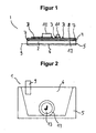
- FIG. 1 is a cross section through a non-limiting embodiment of a molded article according to the invention, here an operating panel 1, shown.
- an operating panel 1 In the control panel 1 is on a first side (front) 4 of a glass sheet 2 as a substrate Protective lacquer layer 6 applied from a cured lacquer. Between the glass sheet 1 and the protective lacquer layer 6, a tab made of a plastic, in this case polypropylene, is applied as a peel-off aid 9 for the cured protective lacquer layer 6.
- a tab made of a plastic in this case polypropylene
- two color layers 7 and 8 are applied, which may have recesses 12.
- conductor structure layers 3 to which electronic components 10, in particular a pressure-sensitive sensor 11, can be fastened, for example via a solder connection.
- the substrate 2 which in the FIG. 1 a glass plate is provided. Thereafter, a layer 8 and then a layer 9 is applied by screen printing on the back, ie first surface of the substrate first. It is also possible that certain areas of the back of substrate 2 are not coated.
- an intermediate drying step is carried out at about 100 to 150 ° C. after the application of a color layer 8 or 9.
- At least one layer of conductive patterns of burnable conductive paste 3 is applied to the back surface of substrate 2, i. on the substrate 2 or on the color layer 7 or 8, applied.
- Conductor structures include electronic elements such as resistors or sensor elements.
- All coatings and other components such as electronic components or terminals are mounted on the first surface of the substrate so that the second surface forms a closed surface.
- Fig. 2 shows a plan view of a molded body according to the invention according to a second embodiment of the invention, which is also an operating panel here.
- a peelable protective lacquer layer 6 is partially applied on the user surface of the control panel facing the second surface 5 of the substrate 2.
- a tab is applied as a peel-off aid 9 between the peelable protective lacquer layer 6 and the second surface 5.
- the protective lacquer layer 6 is arranged around recessed areas 13 and 14 on the second surface 5. At these locations it was possible to machine the second surface 5 of substrate 2, without damaging further areas of the second surface due to the lack of protective lacquer.
- the first area 13 is a function selection area corresponding to an upper hierarchical level
- the second area 14 is a specific selection area corresponding to a lower hierarchical level.
- a user can select a function by touching the first area 13, and the function can be made closer by touching a finger over the second area 14 (submenu; intensity).
- the surfaces of the regions 13 and 14 differ, wherein the region 14 here is designed to be frosted and, moreover, can be slightly recessed for easier recording of a finger.
Abstract
Description
Die Erfindung betrifft einen Formkörper mit einem Substrat mit einer ablösbaren Schutzlackschicht sowie ein bevorzugtes Verfahren zu dessen Herstellung.The invention relates to a molding having a substrate with a removable protective lacquer layer and a preferred method for its preparation.
Bei der Weiterverarbeitung von Substraten, die z.B. aus Metall, Glas, Glaskeramik oder Keramik bestehen, werden häufig an einem Teil der Oberfläche mehrere Bearbeitungsschritte durchgeführt, um dem Substrat bestimmte Eigenschaften oder Funktionen zu verleihen.In the further processing of substrates, e.g. Made of metal, glass, glass ceramic or ceramic, often on one part of the surface several processing steps are carried out to give the substrate certain properties or functions.
Beispielsweise ist es bekannt, Glas als Substrat für Bedienfelder (Bedienpanele) in Haushaltgeräten sowie in Geräten der Unterhaltungselektronik einzusetzen. Bei diesen Bedienfeldern sind auf einem Substrat aus Glas bestimmte Bedienungselemente angeordnet, die der Auswahl und Steuerung von Funktionen des zu bedienenden Gerätes dienen. Zur Herstellung werden diese Substrate auf einer einem Benutzer zugewandten Seite sowie auf einer dem Benutzer abgewandten Seite bestimmten Bearbeitungsschritten unterzogen. Beispielsweise können berührungsempfindliche Sensoren angebracht werden, bei denen am Ort des Sensors auf der dem Benutzer zugewandten Seite ein oder mehrere Bereiche mit einer bestimmten Oberflächenbeschaffenheit (Griffmulden, Bereiche unterschiedlicher Oberflächenrauheit, Farbe, usw.) vorgesehen sind. Die Bearbeitung von solchen Substraten ist also häufig auf bestimmte Bereiche der Oberflächen beschränkt. Andererseits werden auf einer dem Benutzer abgewandten Seite solcher Glassubstrate (Glasscheiben) häufig ein oder mehrere Farbschichten aufgetragen, wobei je nach gewünschtem Zweck bestimmte Bereiche so ausgestaltet sind, dass sie transparent oder transluzent sind. In diesen Fällen sind hinter der Glasscheibe häufig eine Beleuchtungseinheit und/oder ein Display zur Anzeige bestimmter Symbole oder Buchstaben angeordnet.For example, it is known to use glass as a substrate for control panels (control panels) in household appliances and in consumer electronics. In these panels, certain operating elements are arranged on a glass substrate, which serve to select and control functions of the device to be operated. For production, these substrates are subjected to certain processing steps on a side facing a user and on a side facing away from the user. For example, touch-sensitive sensors can be attached, in which at the location of the sensor on the side facing the user one or more areas with a specific surface finish (recessed grips, areas of different surface roughness, color, etc.) are provided. The processing of such substrates is thus often limited to certain areas of the surfaces. On the other hand, on one side of such glass substrates (glass panes) facing away from the user, one or more color layers are frequently applied, wherein, depending on the desired purpose, certain areas are designed such that they are transparent or translucent. In these cases, a lighting unit and / or a display for displaying certain symbols or letters are often arranged behind the glass.
Bei der Herstellung durchlaufen derartige Bedienpanele somit mehrere Bearbeitungsschritte. So wird auf die erste Oberfläche eines dielektrischen Substrates im Allgemeinen nicht nur eine Leiterschicht, sondern zusätzliche Schichten, z.B. Farbschichten aufgebracht. Anschließend erfolgt zur Herstellung der Bedienpanele im Allgemeinen noch eine Bestückung mit elektronischen Bauteilen. Die Bestückung und Befestigung (z.B. durch Löten) mit elektronischen Bauteilen erfolgen häufig örtlich getrennt von der Beschichtung des dielekrischen Substrats. Wünschenswert wäre es jedenfalls, wenn die zweite Oberfläche des Substrates während dieser Bearbeitungsschritte und/oder nach Durchführung der Herstellungsschritte vor mechanischen oder chemischen Einwirkungen geschützt werden könnte.In the manufacture of such control panels thus undergo several processing steps. Thus, on the first surface of a dielectric substrate generally not only a conductor layer, but additional layers, such as color layers are applied. Subsequently, the production of the control panels is generally followed by an assembly with electronic components. The assembly and mounting (eg by Soldering) with electronic components are often carried out locally separated from the coating of the dielectric substrate. In any case, it would be desirable if the second surface of the substrate could be protected from mechanical or chemical effects during these processing steps and / or after carrying out the production steps.
Jedenfalls kann es bei der Bearbeitung von Glassubstraten aber auch von anderen Substraten, durch Stoß, Berührung mit scharfen Gegenständen usw. zu Beschädigungen kommen, die entweder zu zeit- oder kostenaufwändigen Reparaturen, zu dauerhaften Schädigungen oder bei gravierenden Beschädigungen sogar zu einem vollständigen Verlust des Formkörpers führen.In any case, it may be in the processing of glass substrates but also from other substrates, by impact, contact with sharp objects, etc. damage, either to time-consuming or costly repairs to permanent damage or serious damage even to a complete loss of the molding to lead.
Die
Die
Die
Aufgabe der Erfindung war es vor diesem Hintergrund, einen Formkörper, umfassend ein Substrat aus einem Metall, Glas, Glaskeramik oder Keramik, bereitzustellen, bei dem das Substrat bei seiner Bearbeitung hinsichtlich Beschädigungen seiner Oberfläche geschützt ist und bei dem dieser Schutz die spätere Verwendung des Formkörper nicht beeinträchtigt. Aufgabe der Erfindung war außerdem die Bereitstellung eines Verfahrens zu seiner Herstellung.Against this background, the object of the invention was to provide a shaped body comprising a substrate made of a metal, glass, glass ceramic or ceramic, in which the Substrate is protected during its processing in terms of damage to its surface and in which this protection does not affect the subsequent use of the molding. The object of the invention was also to provide a method for its production.
Die Lösung dieser Aufgabe wird nach dieser Erfindung erreicht durch einen Formkörper sowie ein Verfahren zu seiner Herstellung mit den Merkmalen der entsprechenden unabhängigen Patentansprüche. Bevorzugte Ausführungsformen des erfindungsgemäßen Formkörpers sind in entsprechenden abhängigen Patentansprüchen aufgeführt. Bevorzugten Ausführungsformen des erfindungsgemäßen Formkörpers entsprechen bevorzugte Ausführungsformen des erfindungsgemäßen Verfahrens und umgekehrt, selbst wenn dies hierin nicht explizit festgestellt wird.The solution of this object is achieved according to this invention by a molding and a method for its preparation with the features of the corresponding independent claims. Preferred embodiments of the shaped body according to the invention are listed in corresponding dependent claims. Preferred embodiments of the shaped body according to the invention correspond to preferred embodiments of the method according to the invention and vice versa, even if this is not explicitly stated herein.
Gegenstand der Erfindung ist somit ein Formkörper, umfassend ein Substrat aus einem Metall, Glas, Glaskeramik oder Keramik mit einer ersten Oberfläche und einer zweiten Oberfläche, wobei das Substrat auf mindestens einem Teil seiner ersten und/oder zweiten Oberfläche eine Schutzschicht aufweist, welche eine ablösbare Schutzlackschicht ist.The invention thus relates to a shaped body, comprising a substrate made of a metal, glass, glass ceramic or ceramic having a first surface and a second surface, wherein the substrate has a protective layer on at least a part of its first and / or second surface, which has a removable Protective lacquer layer is.
"Ablösbare Schutzlackschicht" im Sinne der Erfindung bedeutet, dass die Schutzlackschicht vom Substrat entfernt werden kann, ohne dass hierdurch das Substrat beschädigt wird. Vorzugsweise kann die Schutzlackschicht mechanisch, insbesondere durch Abziehen durch einen Benutzer abgelöst werden."Peelable protective lacquer layer" in the sense of the invention means that the protective lacquer layer can be removed from the substrate without damaging the substrate. Preferably, the protective lacquer layer can be removed mechanically, in particular by peeling off by a user.
Der Begriff "Schutzlackschicht" bedeutet insbesondere eine Schicht aus einem gehärteten Lack. Der Begriff "Lack", wie er hierin verwendet wird, bedeutet dagegen im Allgemeinen eine noch fließfähige Zusammensetzung, die auf das Substrat zur Erzeugung der Schutzlackschicht aufgebracht werden kann.The term "protective lacquer layer" means in particular a layer of a cured lacquer. In contrast, the term "paint" as used herein generally means a still flowable composition that can be applied to the substrate to form the protective lacquer layer.
Das Substrat im Sinne der vorliegenden Erfindung ist vorzugsweise ein dielektrisches Substrat wie z.B. Glas, Glaskeramik oder Glas. Bevorzugt ist das Substrat Glas, insbesondere eine Glasplatte, im Allgemeinen eine Floatglasplatte. Ganz besonders bevorzugt besteht das Substrat aus Einscheibensicherheitsglas. Dann ist der Formkörper besonders bruchfest und auch bei hohen Temperaturen noch stabil.The substrate in the sense of the present invention is preferably a dielectric substrate such as e.g. Glass, glass ceramic or glass. The substrate is preferably glass, in particular a glass plate, generally a float glass plate. Most preferably, the substrate is made of toughened safety glass. Then the molded body is particularly resistant to breakage and still stable at high temperatures.
In einer bevorzugten Ausführungsform des erfindungsgemäßen Formkörpers ist der Schutzlack der Schutzlackschicht ein durch Einwirkung von Wärme und/oder Strahlung gehärteter Lack, wobei der Lack eine härtbare, insbesondere durch Einwirkung von Wärme oder Licht, Zusammensetzung aus polymerisierbaren Monomeren und/oder vernetzbaren Oligomeren und/oder Polymeren umfasst. Hierbei ist es bevorzugt, dass die härtbare Zusammensetzung einen Feststoffgehalt von mindestens 90 % aufweist.In a preferred embodiment of the shaped body according to the invention, the protective lacquer of the protective lacquer layer is a by the action of heat and / or radiation hardened lacquer, wherein the lacquer comprises a curable, in particular by the action of heat or light, composition of polymerizable monomers and / or crosslinkable oligomers and / or polymers. Here, it is preferred that the curable composition has a solids content of at least 90%.
Der Formkörper ist erfindungsgemäß nicht besonders beschränkt, da bei zahlreichen Formkörpern häufig ein Substrat in Hinblick auf eine mögliche Beschädigung zu schützen ist.According to the invention, the shaped body is not particularly limited, since with numerous shaped bodies, it is often necessary to protect a substrate with regard to possible damage.
Besonders bevorzugt umfasst der Formkörper ein Bedienpanel, welches wiederum vorzugsweise ein dielektrisches Substrat aus Glas, Glaskeramik oder Keramik mit einer ersten Oberfläche und einer zweiten Oberfläche umfasst, wobei eine Schicht mit Leiterstrukturen auf der ersten Oberfläche und eine abziehbare Schutzlackschicht auf der zweiten Oberfläche angeordnet ist. Hierbei weist das Bedienpanel vorzugsweise einen berührungsempfindlichen Sensor auf. Erfindungsgemäß sind als berührungsempfindliche Sensoren kapazitive Sensoren bevorzugt. Überdies ist es bevorzugt, dass zwischen der Schicht mit Leiterstrukturen auf der ersten Oberfläche des Substrats und dem Substrat mindestens eine Schicht aus einem Farblack angeordnet ist.Particularly preferably, the molded body comprises a control panel, which in turn preferably comprises a dielectric substrate of glass, glass ceramic or ceramic having a first surface and a second surface, wherein a layer having conductor patterns on the first surface and a peelable protective lacquer layer on the second surface is arranged. In this case, the control panel preferably has a touch-sensitive sensor. According to the invention, capacitive sensors are preferred as touch-sensitive sensors. Moreover, it is preferred that at least one layer of a colored lacquer is arranged between the layer with conductor structures on the first surface of the substrate and the substrate.
Bei Bedienpanelen befinden sich im Allgemeinen sämtliche Leiterstrukturen, Lötverbindungen und elektronischen Bauteile, und ggf. weitere Komponenten auf einer dem Benutzer des Bedienpanels abgewandten Seite des Substrates.In control panels are generally all the conductor structures, solder joints and electronic components, and possibly other components on a side facing away from the user of the control panel side of the substrate.
Beim erfindungsgemäßen Formkörper ist vorzugsweise eine Abziehhilfe angebracht. Die Abziehhilfe ist vorzugsweise eine Lasche, die von einem Benutzer ergriffen werden kann, der dadurch den Schutzlack vom Substrat abziehen kann. Die Lasche sollte ausreichend stabil sein, um von einem Benutzer gegriffen werden zu können. Ansonsten ist die Abziehhilfe möglichst dünn, wobei die Dicke von der Natur des gewählten Materials und der gewünschten Steifigkeit der Abziehhilfe abhängt. Als Material der Abziehhilfe wird vorzugsweise ein Kunststoff, insbesondere ein thermoplastischer Kunststoff gewählt, beispielsweise aus Polypropylen.In the case of the shaped body according to the invention, a removal aid is preferably attached. The peel aid is preferably a tab that can be grasped by a user who can thereby peel off the resist from the substrate. The tab should be stable enough to be gripped by a user. Otherwise, the peel-off aid is as thin as possible, the thickness depending on the nature of the material chosen and the desired stiffness of the peel-off aid. The material of the removal aid is preferably a plastic, in particular a thermoplastic chosen, for example polypropylene.
Eine an der Schutzlackschicht angebrachte Abziehhilfe kann sich innerhalb des Schutzlackes aber auch zwischen Substrat und Schutzlack befinden.A peel-off aid attached to the protective lacquer layer can be located within the protective lacquer but also between the substrate and the protective lacquer.
Die Schutzschicht hat im Allgemeinen eine Dicke von 0,05 bis 0,5 mm.The protective layer generally has a thickness of 0.05 to 0.5 mm.
In einer besonders bevorzugten Ausführungsform des Formkörpers umfasst die ablösbare Schutzlackschicht einen Lötabdecklack oder besteht aus diesem.In a particularly preferred embodiment of the molded article, the removable protective lacquer layer comprises or consists of a solder masking lacquer.
Gegenstand der Erfindung ist außerdem ein Verfahren zur Herstellung eines Formkörpers, der ein Substrat aus einem Metall, Glas, Glaskeramik oder Keramik mit einer ersten Oberfläche und einer zweiten Oberfläche umfasst, wobei das Substrat auf mindestens einem Teil seiner ersten und/oder zweiten Oberfläche eine ablösbare Schutzlackschicht aufweist, umfassend die Schritte
- (a) Aufbringen eines Lackes, wobei der Lack eine durch Einwirkung von Wärme und/oder Strahlung härtbare Zusammensetzung aus polymerisierbaren Monomeren und/oder vernetzbaren Oligomeren und/oder Polymeren umfasst, auf zumindest einen Teil einer ersten Oberfläche und/oder einer zweite Oberfläche des Substrats; und
- (b) Härten des Lackes durch Einwirkung von Wärme und/oder Strahlung.
- (a) applying a lacquer, wherein the lacquer comprises a heat and / or radiation curable composition of polymerizable monomers and / or crosslinkable oligomers and / or polymers, on at least a portion of a first surface and / or a second surface of the substrate ; and
- (B) hardening of the paint by the action of heat and / or radiation.
In einer bevorzugten Ausführungsform dieses Verfahrens wird der Lack mittels Siebdruck auf der ersten und/oder zweiten Oberfläche aufgebracht.In a preferred embodiment of this method, the paint is applied by screen printing on the first and / or second surface.
Der härtbare Lack weist vorzugsweise einen Feststoffgehalt von mindestens 90 % auf, und weist besonders bevorzugt einen Feststoffgehalt von mindestens 95 % auf, bezogen auf die Gesamtmasse des Lackes, gemäß DIN EN ISO 3251 (1 h, 125°C, 1g Einwaage).The curable lacquer preferably has a solids content of at least 90%, and particularly preferably has a solids content of at least 95%, based on the total mass of the lacquer, according to DIN EN ISO 3251 (1 h, 125 ° C, 1 g weight).
Der härtbare Lack weist vorzugsweise ein wässriges Lösungsmittel auf. Insbesondere enthält der härtbare Lack vorzugsweise keine organischen Lösungsmittel.The curable lacquer preferably comprises an aqueous solvent. In particular, the curable lacquer preferably contains no organic solvents.
Darüberhinaus liegt eine Viskosität des härtbaren Lackes gemäß DIN EN ISO 3219 bei 20°C vorzugsweise in einem Bereich von 10000 bis 80000 mPas. Diese Viskosität kann beispielsweise mit einem Viskositätsmeßgerät Haake RS 600, C 20/1 °, D = 50 s-1 der Firma Electron GmbH gemessen werden.In addition, a viscosity of the curable lacquer according to DIN EN ISO 3219 at 20 ° C. is preferably in a range from 10,000 to 80,000 mPas. This viscosity can be measured, for example, with a Haake RS 600, C 20/1 °, D = 50 s-1 viscometer from Electron GmbH.
Vorzugsweise ist der härtbare Lack thixotrop.Preferably, the curable lacquer is thixotropic.
Im Allgemeinen umfasst der Schutzlack einen durch Wärme- und/oder Strahleneinwirkung gehärteten Lack, wobei der Lack eine Zusammensetzung aus polymerisierbaren Monomeren und/oder vernetzbaren Oligomeren und/oder Polymeren ist. Der Schutzlack umfasst vorzugsweise Epoxidharze, Polybutadiene, Polyurethane, insbesondere mit Carboxyl- oder Hydroxylendgruppen, sowie deren Mischungen und Reaktionsprodukte.In general, the protective lacquer comprises a heat and / or radiation-cured lacquer, wherein the lacquer is a composition of polymerizable monomers and / or crosslinkable oligomers and / or polymers. The protective lacquer preferably comprises epoxy resins, polybutadienes, polyurethanes, in particular having carboxyl or hydroxyl end groups, and mixtures and reaction products thereof.
Der im Formkörper, z.B. Bedienpanel, eingesetzte härtbare Lack ist vorzugsweise ein Lötabdecklack. Vorzugsweise wird hierbei ein Lötabdecklack mit einer hohen Wärmestabilität eingesetzt. Dies ermöglicht auch mehrfache Temperaturbelastungen sowie den Einsatz in Verbindung mit bleifreien Lötprozessen. Insbesondere ist die Wärmestabilität vorzugsweise so hoch, dass auch ein Reflow-Löten möglich ist.The in the shaped body, e.g. Control panel, used curable lacquer is preferably a solder mask. Preferably, in this case a Lötabdecklack is used with a high thermal stability. This also allows multiple temperature loads as well as the use in connection with lead-free soldering processes. In particular, the heat stability is preferably so high that reflow soldering is also possible.
Besonders geeignete Schutzlacke sind die Lötabdecklacke der Reihe SD 2950 der Firma Lackwerke Peters GmbH + Co KG.Particularly suitable protective lacquers are the solder masking lacquers of the series SD 2950 from Lackwerke Peters GmbH + Co KG.
Bei Verwendung eines dielektrischen Substrats ist dieses vorzugsweise transparent oder semitransparent. Ein Farbaufdruck auf der ersten Seite ist dann vorzugsweise erkennbar.When using a dielectric substrate, it is preferably transparent or semi-transparent. A color print on the first page is then preferably recognizable.
Die Erfindung hat zahlreiche Vorteile. So wird ein Formkörper, der ein Substrat umfasst, beispielsweise aus einem Metall, aber insbesondere aus einem dielektrischen Material wie Glas, Glaskeramik und Keramik, vor Beschädigungen oder sonstigen Beeinträchtigungen der Oberfläche des Substrats geschützt. So kann gemäß der Erfindung beispielsweise ein Bedienpanel bereitgestellt werden, bei dem das dielektrische Substrat während und nach der Herstellung des Bedienpanels geschützt wird. Die vorliegende Erfindung ermöglicht aber den Schutz sowohl von einfachen Formkörpern, z.B. von Glasscheiben, die weder bedruckt noch mit elektronischen Elementen bestückt sind, als auch von komplexen Formkörpern, die beispielsweise Sensoren und elektronische Schaltkreise enthalten und auch mit Farblacken bedruckt sein können.The invention has numerous advantages. Thus, a shaped body comprising a substrate, for example of a metal, but in particular of a dielectric material such as glass, glass ceramic and ceramic, is protected from damage or other impairment of the surface of the substrate. Thus, according to the invention, for example, a control panel can be provided in which the dielectric substrate is protected during and after the manufacture of the control panel. However, the present invention makes it possible to protect both simple moldings, e.g. of glass panes which are neither printed nor equipped with electronic elements, as well as of complex shaped bodies, which contain, for example, sensors and electronic circuits and can also be printed with colored lacquers.
Die Erfindung wird im Folgenden anhand zweier nicht einschränkend gemeinter Ausführungsbeispiele für einen erfindungsgemäßen Formkörper illustriert.
-
Fig. 1 zeigt einen Querschnitt durch einen erfindungsgemäßen Formkörper gemäß einer ersten Ausführungsform der Erfindung, welcher hier ein Bedienpanel ist. -
Fig. 2 zeigt eine Draufsicht auf einen erfindungsgemäßen Formkörper gemäß einer zweiten Ausführungsform der Erfindung, welches hier ebenfalls ein Bedienpanel ist.
-
Fig. 1 shows a cross section through a molding according to the invention according to a first embodiment of the invention, which is here a control panel. -
Fig. 2 shows a plan view of a molded body according to the invention according to a second embodiment of the invention, which is also an operating panel here.
In der
Auf der zweiten Seite (Rückseite) von Substrat 2 sind zwei Farbschichten 7 und 8 aufgebracht, die Aussparungen 12 aufweisen können. Auf den Farbschichten 7 und 8 sind Leiterstrukturschichten 3 angeordnet, an denen elektronische Bauteile 10, insbesondere ein druckempfindlicher Sensor 11, befestigt sein können, beispielsweise über eine Lötverbindung.On the second side (rear side) of
Zur Durchführung des erfindungsgemäßen Verfahrens wird bei der hier gezeigten nicht einschränkend gemeinten Ausführungsform in einem ersten Schritt das Substrat 2, welches in der
Bei der hier gezeigten vorteilhaften Ausführungsform der Erfindung erfolgt nach dem Aufbringen einer Farbschicht 8 oder 9 jeweils ein Zwischentrockenschritt bei etwa 100 bis 150°C.In the advantageous embodiment of the invention shown here, an intermediate drying step is carried out at about 100 to 150 ° C. after the application of a
Danach wird mittels Siebdruck mindestens eine Schicht von Leiterstrukturen aus einbrennbarer Leitpaste 3 auf die Rückseite von Substrat 2, d.h. auf das Substrat 2 oder auf die Farbschicht 7 oder 8, aufgetragen. Leiterstrukturen umfassen elektronische Elemente wie Widerstände oder Sensorelemente. Nach dem Aufbringen aller Farbschichten 7 und 8 und der Leitpaste für die Bildung der Leiterstrukturschicht 3 erfolgt das Einbrennen dieser Schichten in einem Schritt. Die Einbrenntemperatur liegt dabei im Bereich von 600 bis 700°C und beträgt vorzugsweise etwa 620°C.Thereafter, by screen printing, at least one layer of conductive patterns of burnable
Alle Beschichtungen und weitere Komponenten wie elektronische Bauteile oder Anschlüsse sind auf der ersten Oberfläche des Substrats angebracht, so dass die zweite Oberfläche eine geschlossene Oberfläche bildet.All coatings and other components such as electronic components or terminals are mounted on the first surface of the substrate so that the second surface forms a closed surface.
Auf der dem Benutzer des Bedienpanels zugewandten zweiten Oberfläche 5 des Substrats 2 ist teilweise eine abziehbare Schutzlackschicht 6 aufgebracht. Zur leichteren Entfernbarkeit von Schutzlackschicht 6 ist zwischen der abziehbaren Schutzlackschicht 6 und der zweiten Oberfläche 5 eine Lasche als Abziehhilfe 9 aufgebracht. Die Schutzlackschicht 6 ist um ausgesparte Bereiche 13 und 14 auf der zweiten Oberfläche 5 angeordnet. An diesen Stellen war es aufgrund des nichtvorhandenen Schutzlackes möglich, die zweite Oberfläche 5 von Substrat 2 zu bearbeiten, ohne dass weitere Bereiche der zweiten Oberfläche beschädigt wurden. Bei der hier gezeigten Ausführungsform ist der erste Bereich 13 ein Funktionsauswahlbereich entsprechend einer oberen Hierarchieebene und der zweite Bereich 14 ein spezifischer Auswahlbereich entsprechend einer unteren Hierarchieebene. D.h., dass ein Benutzer durch Berühren des ersten Bereiches 13 eine Funktion auswählen kann, wobei durch Berühren bzw. durch Ziehen eines Fingers über den zweiten Bereich 14 die Funktion näher ausgestaltet werden kann (Untermenü; Intensität). Bei der hier gezeigten Ausführungsform unterscheiden sich die Oberflächen der Bereiche 13 und 14, wobei der Bereich 14 hier mattiert ausgestaltet ist und außerdem zur leichteren Aufnahme eines Fingers leicht vertieft ausgebildet sein kann.On the user surface of the control panel facing the
- 11
- Formkörper, hier BedienpanelShaped body, here operating panel
- 22
- Substrat, hier GlasscheibeSubstrate, here glass pane
- 33
- Leiterstrukturconductor structure
- 44
- Erste Oberfläche des SubstratsFirst surface of the substrate
- 55
- Zweite Oberfläche des SubstratsSecond surface of the substrate
- 66
- SchutzlackschichtProtective lacquer layer
- 77
- Erste FarbschichtFirst coat of paint
- 88th
- Zweite FarbschichtSecond layer of paint
- 99
- Abziehhilfe, LaschePuller, tab
- 1010
- Elektronisches BauelementElectronic component
- 1111
- Berührungsempfindlicher (druckempfindlicher) SensorTouch-sensitive (pressure-sensitive) sensor
- 1212
- Aussparungrecess
- 1313
- Funktionsauswahlbereich (obere Hierarchieebene)Function selection area (upper hierarchy level)
- 1414
- Spezifischer Auswahlbereich (untere Hierarchieebene)Specific selection area (lower hierarchy level)
Claims (12)
Applications Claiming Priority (1)
| Application Number | Priority Date | Filing Date | Title |
|---|---|---|---|
| DE102010063308.9A DE102010063308B4 (en) | 2010-12-16 | 2010-12-16 | Control panel with a substrate with removable protective coating and process for its production |
Publications (1)
| Publication Number | Publication Date |
|---|---|
| EP2467000A1 true EP2467000A1 (en) | 2012-06-20 |
Family
ID=45445791
Family Applications (1)
| Application Number | Title | Priority Date | Filing Date |
|---|---|---|---|
| EP11193939A Withdrawn EP2467000A1 (en) | 2010-12-16 | 2011-12-16 | Moulded part with a substrate with removable protective varnish coating and method for producing same |
Country Status (2)
| Country | Link |
|---|---|
| EP (1) | EP2467000A1 (en) |
| DE (1) | DE102010063308B4 (en) |
Citations (11)
| Publication number | Priority date | Publication date | Assignee | Title |
|---|---|---|---|---|
| DE19652728A1 (en) * | 1995-12-23 | 1997-06-26 | Volkswagen Ag | Application of peelable protective film to lacquered vehicle bodywork |
| US5945462A (en) * | 1997-10-02 | 1999-08-31 | Loctite Corporation | Temporary protective coatings for precision surfaces |
| EP0941291B1 (en) * | 1996-11-28 | 2001-02-07 | E.I. Du Pont De Nemours And Company | Process for preparing temporary protective coatings |
| US20050167416A1 (en) * | 2002-04-10 | 2005-08-04 | Eurokera S.N.C. | Glass-ceramic plates, method for making same and cooking surface equipped with same |
| DE102004026672A1 (en) * | 2004-05-28 | 2005-12-29 | Schott Ag | Contact switch has electrically conducting layer arranged on side remote from user structured in at least one electrically isolated flat region defining at least one capacitive contact or touch sensor electrode |
| US6991851B2 (en) * | 2001-10-03 | 2006-01-31 | 3M Innovative Properties Company | Dry-peelable temporary protective coatings |
| DE102004047800A1 (en) * | 2004-09-29 | 2006-04-06 | Schott Ag | Temporary protection of glass substrates comprises applying polymer protective layer at glass substrate and removing polymer protective layer by plasma etching procedure after fulfilling protective function of glass substrate |
| EP1705163A1 (en) | 2005-03-24 | 2006-09-27 | Irlbacher Blickpunkt Glas GmbH | Control panel |
| EP1487759B1 (en) | 2002-03-13 | 2007-05-23 | Electrovac AG | Method for the production of a metal-ceramic substrate, preferably a copper-ceramic substrate |
| DE102005054562A1 (en) | 2005-11-14 | 2007-07-05 | Peters Research Gmbh + Co. Kg | The solder stop varnish for circuit boards, which can be photo structured, is formulated to include a cold blend powder varnish resin |
| WO2012027133A2 (en) * | 2010-08-24 | 2012-03-01 | Corning Incorporated | Method of strengthening edge of glass article |
Family Cites Families (1)
| Publication number | Priority date | Publication date | Assignee | Title |
|---|---|---|---|---|
| JP3254572B2 (en) | 1996-06-28 | 2002-02-12 | バンティコ株式会社 | Photopolymerizable thermosetting resin composition |
-
2010
- 2010-12-16 DE DE102010063308.9A patent/DE102010063308B4/en not_active Expired - Fee Related
-
2011
- 2011-12-16 EP EP11193939A patent/EP2467000A1/en not_active Withdrawn
Patent Citations (12)
| Publication number | Priority date | Publication date | Assignee | Title |
|---|---|---|---|---|
| DE19652728A1 (en) * | 1995-12-23 | 1997-06-26 | Volkswagen Ag | Application of peelable protective film to lacquered vehicle bodywork |
| EP0941291B1 (en) * | 1996-11-28 | 2001-02-07 | E.I. Du Pont De Nemours And Company | Process for preparing temporary protective coatings |
| US5945462A (en) * | 1997-10-02 | 1999-08-31 | Loctite Corporation | Temporary protective coatings for precision surfaces |
| US6991851B2 (en) * | 2001-10-03 | 2006-01-31 | 3M Innovative Properties Company | Dry-peelable temporary protective coatings |
| EP1487759B1 (en) | 2002-03-13 | 2007-05-23 | Electrovac AG | Method for the production of a metal-ceramic substrate, preferably a copper-ceramic substrate |
| US20050167416A1 (en) * | 2002-04-10 | 2005-08-04 | Eurokera S.N.C. | Glass-ceramic plates, method for making same and cooking surface equipped with same |
| DE102004026672A1 (en) * | 2004-05-28 | 2005-12-29 | Schott Ag | Contact switch has electrically conducting layer arranged on side remote from user structured in at least one electrically isolated flat region defining at least one capacitive contact or touch sensor electrode |
| DE102004047800A1 (en) * | 2004-09-29 | 2006-04-06 | Schott Ag | Temporary protection of glass substrates comprises applying polymer protective layer at glass substrate and removing polymer protective layer by plasma etching procedure after fulfilling protective function of glass substrate |
| EP1705163A1 (en) | 2005-03-24 | 2006-09-27 | Irlbacher Blickpunkt Glas GmbH | Control panel |
| DE102005013884A1 (en) | 2005-03-24 | 2006-09-28 | Irlbacher Blickpunkt Glas Gmbh | control panel |
| DE102005054562A1 (en) | 2005-11-14 | 2007-07-05 | Peters Research Gmbh + Co. Kg | The solder stop varnish for circuit boards, which can be photo structured, is formulated to include a cold blend powder varnish resin |
| WO2012027133A2 (en) * | 2010-08-24 | 2012-03-01 | Corning Incorporated | Method of strengthening edge of glass article |
Also Published As
| Publication number | Publication date |
|---|---|
| DE102010063308A1 (en) | 2012-06-21 |
| DE102010063308B4 (en) | 2019-01-24 |
Similar Documents
| Publication | Publication Date | Title |
|---|---|---|
| DE10143523B4 (en) | Process for the preparation of a selectively metallised film | |
| DE102009036161B4 (en) | Sensor element device and method for producing a sensor element device | |
| DE112016005211T5 (en) | Plate with a print layer, display device using it, and glass with a functional layer for display device in a vehicle | |
| DE20122195U1 (en) | Carrier substrate for electronic components | |
| DE102015100297A1 (en) | Flexible electrical conductor structure | |
| EP1705163B1 (en) | Control panel | |
| EP2194594B1 (en) | Method for producing a three-dimensional component | |
| EP3312147B1 (en) | Method for manufacturing a decorative cover | |
| DE102010063308B4 (en) | Control panel with a substrate with removable protective coating and process for its production | |
| EP2833248A1 (en) | Capacitive sensor device with electrically conductive coated sensor board made of glass | |
| WO2014170117A1 (en) | Component having a structured surface and method for the production thereof | |
| EP1982002A1 (en) | Process for producing partially metallized substrates | |
| EP0616905B1 (en) | Sanitary tapware with coated surface and process for its manufacture | |
| DE1965493A1 (en) | Transfer paper for the production of printed circuits | |
| DE102012201600B4 (en) | Capacitive sensor device with a spring contact | |
| DE102011002077B4 (en) | Method for producing a plastic workpiece provided with at least one electrical functional part | |
| DE102009032816A1 (en) | Lacquer foil product for providing jointless surface over display embedded in dashboard in motor vehicle, has foil layer with electrically conductive layer made of plastic material and providing actuating element | |
| DE202020100474U1 (en) | Electrically conductive laserable paint and this comprehensive touch control element | |
| DE102019126908A1 (en) | Process for the production of functional objects, functional object | |
| DE102007058715A1 (en) | Laminar decoration element e.g. decoration foil, for interior of motor vehicle, has partial transparent substrate with upper and lower surfaces, where three dimensional structures are imprinted on upper and lower surfaces, respectively | |
| DE102006027263A1 (en) | Substrate with a layer sequence for producing a color impression which changes as a function of the viewing angle | |
| WO2016058593A1 (en) | Method for producing a molded item and a covering layer for use with the method | |
| EP2199321A1 (en) | Method for coating polymeric plastic substrates | |
| DE102011089454A1 (en) | Operating device for electric appliance, has operating element and operating panel with operating panel-front side and operating panel-rear side, where piezo-sensor element is arranged on operating panel-rear side | |
| EP1746208A1 (en) | Process for preparing a partially metallized substrate. |
Legal Events
| Date | Code | Title | Description |
|---|---|---|---|
| PUAI | Public reference made under article 153(3) epc to a published international application that has entered the european phase |
Free format text: ORIGINAL CODE: 0009012 |
|
| AK | Designated contracting states |
Kind code of ref document: A1 Designated state(s): AL AT BE BG CH CY CZ DE DK EE ES FI FR GB GR HR HU IE IS IT LI LT LU LV MC MK MT NL NO PL PT RO RS SE SI SK SM TR |
|
| AX | Request for extension of the european patent |
Extension state: BA ME |
|
| STAA | Information on the status of an ep patent application or granted ep patent |
Free format text: STATUS: THE APPLICATION IS DEEMED TO BE WITHDRAWN |
|
| 18D | Application deemed to be withdrawn |
Effective date: 20121221 |