EP2465019B1 - Printed force sensor within a touch screen - Google Patents
Printed force sensor within a touch screen Download PDFInfo
- Publication number
- EP2465019B1 EP2465019B1 EP10737189.0A EP10737189A EP2465019B1 EP 2465019 B1 EP2465019 B1 EP 2465019B1 EP 10737189 A EP10737189 A EP 10737189A EP 2465019 B1 EP2465019 B1 EP 2465019B1
- Authority
- EP
- European Patent Office
- Prior art keywords
- layer
- electrode
- touch screen
- force
- conductive material
- Prior art date
- Legal status (The legal status is an assumption and is not a legal conclusion. Google has not performed a legal analysis and makes no representation as to the accuracy of the status listed.)
- Not-in-force
Links
Images




Classifications
-
- G—PHYSICS
- G06—COMPUTING OR CALCULATING; COUNTING
- G06F—ELECTRIC DIGITAL DATA PROCESSING
- G06F3/00—Input arrangements for transferring data to be processed into a form capable of being handled by the computer; Output arrangements for transferring data from processing unit to output unit, e.g. interface arrangements
- G06F3/01—Input arrangements or combined input and output arrangements for interaction between user and computer
- G06F3/03—Arrangements for converting the position or the displacement of a member into a coded form
- G06F3/041—Digitisers, e.g. for touch screens or touch pads, characterised by the transducing means
- G06F3/0414—Digitisers, e.g. for touch screens or touch pads, characterised by the transducing means using force sensing means to determine a position
-
- G—PHYSICS
- G06—COMPUTING OR CALCULATING; COUNTING
- G06F—ELECTRIC DIGITAL DATA PROCESSING
- G06F3/00—Input arrangements for transferring data to be processed into a form capable of being handled by the computer; Output arrangements for transferring data from processing unit to output unit, e.g. interface arrangements
- G06F3/01—Input arrangements or combined input and output arrangements for interaction between user and computer
- G06F3/03—Arrangements for converting the position or the displacement of a member into a coded form
- G06F3/041—Digitisers, e.g. for touch screens or touch pads, characterised by the transducing means
- G06F3/044—Digitisers, e.g. for touch screens or touch pads, characterised by the transducing means by capacitive means
- G06F3/0445—Digitisers, e.g. for touch screens or touch pads, characterised by the transducing means by capacitive means using two or more layers of sensing electrodes, e.g. using two layers of electrodes separated by a dielectric layer
-
- G—PHYSICS
- G06—COMPUTING OR CALCULATING; COUNTING
- G06F—ELECTRIC DIGITAL DATA PROCESSING
- G06F3/00—Input arrangements for transferring data to be processed into a form capable of being handled by the computer; Output arrangements for transferring data from processing unit to output unit, e.g. interface arrangements
- G06F3/01—Input arrangements or combined input and output arrangements for interaction between user and computer
- G06F3/03—Arrangements for converting the position or the displacement of a member into a coded form
- G06F3/041—Digitisers, e.g. for touch screens or touch pads, characterised by the transducing means
- G06F3/044—Digitisers, e.g. for touch screens or touch pads, characterised by the transducing means by capacitive means
- G06F3/0446—Digitisers, e.g. for touch screens or touch pads, characterised by the transducing means by capacitive means using a grid-like structure of electrodes in at least two directions, e.g. using row and column electrodes
-
- G—PHYSICS
- G06—COMPUTING OR CALCULATING; COUNTING
- G06F—ELECTRIC DIGITAL DATA PROCESSING
- G06F2203/00—Indexing scheme relating to G06F3/00 - G06F3/048
- G06F2203/041—Indexing scheme relating to G06F3/041 - G06F3/045
- G06F2203/04104—Multi-touch detection in digitiser, i.e. details about the simultaneous detection of a plurality of touching locations, e.g. multiple fingers or pen and finger
Definitions
- This invention relates generally to touch-sensitive electronic components, and more particularly to the incorporation of a force sensor within a touch screen.
- such devices typically comprise one or more user-manipulatable elements that provide mechanisms for converting user input into signals, typically electrical signals, that can be received and processed by the modem electronic device.
- user-manipulatable elements can include keyboards, mice, trackballs, joysticks, and other like devices that can be communicationally coupled to the electronic device through either wired or wireless communicational mechanisms.
- touch-based user-input receivers such as a touch screen that can, within the same, or approximately the same area, both display visual information to the user and receive the touch-based input from the user.
- touch screens are designed such that a user's touch to an area of the touch screen is received and interpreted within the context of the visual information, or graphical element, being displayed in, or proximate to, that area.
- Touch screens can be implemented utilizing any of several types of electromechanical mechanisms, including resistive, capacitive, infrared, surface acoustic wave and other like electromechanical mechanisms.
- touch screens implemented utilizing resistive mechanisms typically comprise multiple transparent layers with electrically conductive coatings that are physically separated such that, when the touch screen is depressed by a user, the multiple conductive layers make contact with one another, causing electrical current to flow between them and, thereby, enabling a sensing mechanism to detect the user's touch.
- touch screens implemented utilizing surface acoustic wave mechanisms typically comprise at least one layer through which acoustic waves, generated by transducers attached to the layer, are propagated. When a user touches the layer, the acoustic energy is absorbed and sensors attached to the layer detect such a change and, thereby, detect the user's touch.
- a touch screen implemented with a self capacitance sensing arrangement can comprise at least one layer of charged electrodes and traces such that, when a user touches, or places their finger in close proximity, to the touch screen, the charge from at least one of the charged electrodes is at least partially transferred to the user's finger, thereby affecting the capacitance of the charged electrode and, consequently, enabling a sensing mechanism to detect the user's touch.
- a touch screen implemented with a mutual capacitance sensing arrangement can comprise multiple layers of spatially separated and intersecting conductive traces, such that, at each intersection, a capacitive coupling node is formed.
- WO-A-02/35461 discloses a method and apparatus for discriminating against false touches in a touchscreen system.
- the system is designed to confirm a touch registered by one touch sensor with another touch sensor, preferably of a different sensor type, prior to acting upon the touch (i.e., sending touch coordinates to the operating system). If the touch registered by the first touch sensor is not confirmed by the second touch sensor, the touch is invalidated.
- the strengths of one type of sensor are used to overcome the deficiencies of another type of sensor.
- This system is particularly well suited to meet the demands of an outdoor or semi-outdoor application.
- one or more force sensors are used as the false touch sensor and a projective-capacitive sensor is used as the position coordinate determining sensor.
- a projective-capacitive sensor is used as the false touch sensor.
- US-A-2009/066673 discloses a software compensation method that allows a touch sensitive display to be built using low-cost FSR force sensors
- the compensation method comprises an array of functional compensation modules including filtering, voltage conversion, temperature compensation, humidity compensation, sensor calibration, sensor reading linearization, auto calibration, positioning determination and finally end-user and mechanical calibration.
- US-A-2008/217413 discloses an apparatus and method for providing a radio frequency identification (RFID) card, the card including a card inlay; an antenna positioned on the card inlay, a RFID integrated circuit (IC) on the card inlay, a pressure-sensitive switch including an electrode structure located on or in the card inlay and coupled to the antenna and the RFID IC via the electrode structure, the pressure-sensitive switch having an electrical resistance that varies with a pressure applied to the switch, and a dam of material in a vicinity around of the pressure-sensitive switch to provide a barrier against a lateral pressure being applied to the switch.
- RFID radio frequency identification
- One aspect of the present invention is a force sensor as defined in independent claim 1.
- Another aspect of the invention is a method as defined in independent claim 9. Further embodiments of the invention are specified in the respective appended dependent claims.
- the force sensor can comprise a material that can exhibit changing electrical or magnetic properties as force is applied onto the material, and can further comprise two electrodes oriented on opposite sides of such a material.
- the force sensor can further comprise a force concentrator that can be a protrusion, such as that formed by the electrodes and the force-sensitive material, that can extend beyond the layer plane of a layer of the touch screen.
- the force concentrator can act to absorb all, or substantially all, of a force applied onto the touch screen, thereby transferring that force to the force-sensitive material.
- the electrodes connected to the material can enable detection circuitry to detect any changes in the material's electrical or magnetic properties and can, thereby, enable the detection of a force onto the touch screen.
- a touch screen 110 comprising at least two layers 111 and 112.
- the layers of a touch screen can comprise electromechanical elements that can enable the touch screen 110 to sense touch inputs.
- the touch screen 110 were a resistive touch screen
- each of the layers 111 and 112 could be comprised of conductive materials.
- a touch applied to such a touch screen 110 would cause the layers 111 and 112 to contact one another proximate to the location of the touch, thereby establishing a new conductive path between the two layers and, consequently, providing the basis by which the touch screen 110 could detect the touch.
- the touch screen 110 were a mutually capacitive touch screen, then one of the layers, such as layer 111, could comprise electrodes oriented in one direction, while another of the layers, such as layer 112, could comprise electrodes oriented in a crosswise direction, thereby creating capacitive elements at their intersection.
- a touch applied to such a touch screen 110 would alter the capacitance at one or more of the capacitive intersections and would, thereby, provide the basis by which the touch screen 110 could detect the touch.
- a force sensor 120 can be integrated into such a multi-layer touch screen 110.
- a force-sensitive material 140 can be part of the force sensor 120.
- the force-sensitive material 140 can be any material that can exhibit changing electrical or magnetic properties, such as a changing conductance, as force is applied.
- One such material that can be utilized is a quantum tunneling composite, whose electrical conductance increases as force is applied onto the composite.
- the force sensor 120 can additionally comprise electrodes 130 and 150 positioned on opposite sides of the force-sensitive material 140 such that the electrodes 130 and 150 are electrically coupled by the force-sensitive material 140.
- the electrode 130 can be deposited on or proximate to the layer 112.
- the force-sensitive material 140 can then be layered at least partially on top of the electrode 130 and the electrode 150 can subsequently be layered at least partially on top of the force-sensitive material 140.
- the electrode 130 and the electrode 150 can be aligned to substantially overlap each other on opposite sides of the force-sensitive material 140.
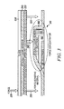
- FIG 2 a two-dimensional cross-sectional slice of the touch screen 110 with an integrated force sensor is shown. More specifically, as will be understood by those skilled in the art, FIG 2 depicts a greatly magnified cross-sectional view of an edge of the touch screen 110 as it rests on a housing 220 of an electronic device incorporating such a touch screen.
- the layers shown in FIG 2 are of substantially planar elements of the touch screen 110 whose three-dimensional form would, in the orientation of the cross-section shown in FIG 2 , extend in to, and out of, the page.
- FIG 2 also shows a cross-section of a portion of the housing 220 of the electronic device incorporating the touch screen 110 and a cross-section of a portion of a display 210.
- the display 210 is typically part of an electronic device incorporating a touch screen, such as the touch screen 110, and is typically oriented such that the visual feedback provided by the display 210, to a user of the electronic device, is aligned with the touch screen, thereby enabling the user to interact with information displayed by the display 210 through the touch screen 110.
- the top layer of a touch screen is a layer of glass 230, or other like material that can provide optical transparency, scratch resistance, and a measure of protection to the layers below.
- An optically clear adhesive 240 such that it does not negatively impact the user's ability to perceive visual information presented by the display 210, can be utilized to connect and bind the glass 230 to lower layers, such as layers that can comprise electrical or magnetic elements that provide for the touch sensing abilities of the touch screen 110.
- electrical or magnetic elements can be incorporated into at least some of the layers of the touch screen 110 to enable the touch screen to utilize, for example, resistive or capacitive mechanisms to sense touch inputs.
- a plastic, or plastic-like, substance can be utilized to carry, or otherwise provide support for, electrical or magnetic elements, such as those described above with reference to layers 111 and 112.
- a PolyEthylene Terephthalate, or "PET” material 250 can provide the structure for, and can comprise, the electrical or magnetic elements referenced above with respect to layer 111.
- the upper PET 250 can comprise the electrodes oriented in one direction, described above in reference to layer 111.
- a similar PET material namely the lower PET 270, can likewise provide the structure for, and can comprise, those complementary electrical or magnetic elements that were referenced above with respect to layer 112.
- the lower PET 270 can comprise the electrodes oriented in a direction crosswise to the electrodes of the upper PET 250, thereby providing capacitive nodes at their intersection, as described above.
- the upper PET 250 can be bound to the glass 230 via the optically clear adhesive 240.
- a similar optically clear adhesive 280 can be utilized to attach the lower PET 270 to lower layers.
- the lower PET 270 can be attached directly to the housing 220 via the optically clear adhesive 280, though, in other embodiments, additional lower layers of the touch screen 110 can be integrated between the lower PET 270 and the housing 220.
- the below-described mechanisms do not require, nor are they intended to be limited to, touch screens utilizing PET layers. Indeed, as will be shown, the below-described mechanisms are equally applicable to any multi-layer touch screen, irrespective of the specific mechanisms utilized to detect touch input, and irrespective of the particular materials utilized to manufacture such a multi-layer touch screen.
- the electrode 130 described previously with reference to FIG 1 , is shown in FIG 2 as being deposited on, and positioned above, the lower PET 270.
- the force-sensitive material 140 also previously described with reference to FIG 1 , whose electrical or magnetic properties change as pressure is applied onto the material, is shown in FIG 2 as being deposited on, and positioned above, at least part of the electrode 130.
- the electrode 150 which was also previously described with reference to FIG 1 , is shown in FIG 2 as being deposited on, and positioned above, at least part of both the electrode 130 and the force-sensitive material 140.
- the electrode 130, force-sensitive material 140 and electrode 150 can be layered one on top of another.
- specific portions of the electrodes 130 and 150, and the force-sensitive material 140, extending along the dimension orthogonal to the page cannot be illustrated.
- the force-sensitive material 140 can extend beyond the boundaries of the electrodes 130 and 150.
- portions of the electrodes 130 and 150 can extend past the force-sensitive material 140 to electrically couple other force sensors, analogous to the force sensor 120, together.
- FIG 2 the cross-section shown in FIG 2 is meant only to be generally illustrative of a specific aspect of the layering of various elements of the touch screen 110, including various elements of the integrated force sensor 120, such as the electrodes 130 and 150 and the force-sensitive material 140.
- the electrode 130 can be deposited on the lower PET 270 through traditional electrode printing technologies, such as printing technologies utilizing conductive or resistive inks to form the electrode 130.
- the force-sensitive material 140 can be deposited on at least a portion of the electrode 130 through printing means.
- a quantum tunneling composite material is utilized, such material is known to be available in an ink, or ink-like, form that can be printed in a manner similar to the printing of the electrode 130.
- the electrode 150 can also be deposited on the force-sensitive material 140, and the lower PET 270, in a similar printed manner, such as through the use of conductive or resistive inks.
- the printing of the electrodes 130 and 150, and of the force-sensitive material 140 can result, not in the rigid, well-defined limits shown in FIG 2 , but in more curved, less well-defined limits. Such natural aspects of a printing process are not detrimental to the operation of the force sensor 120.
- the force-sensitive material 140 can be deposited so as to be between the electrodes 130 and 150, not only vertically, but also horizontally along the lower PET 270.
- the force sensor 120 comprising the electrodes 130 and 150, and the force-sensitive material 140, can be further covered with optically clear adhesive 260 to bind the force sensor 120, and, by proxy, the lower PET 270, to the upper PET 250.
- the optically clear adhesive 260 can simply be layered over the lower PET 270, the electrode 130, the force-sensitive material 140, and the electrode 150.
- the optically clear adhesive can be more precisely applied, such as specifically being applied only to those portions of the force sensor 120 that are in contact with, and thus, can be bound to, the upper PET 250.
- the layering of electrode 130, force-sensitive material 140, electrode 150 and optically clear adhesive 260 can provide a build up of material in the areas of the force sensors that can create a protrusion from the layer plane of the lower PET 270 extending towards the upper PET 250 in at least some instances in excess of other areas that do not similarly have at least some of the layers corresponding to the force sensor.
- any downward pressure applied onto the top of the touch screen 110 such as the glass 230
- the glass 230 and the upper PET 250 will first cause the glass 230 and the upper PET 250 to apply an increased downward pressure at the portions of the glass coinciding with the protrusion formed by the electrode 130, the force-sensitive material 140, the electrode 150 and the optically clear adhesive 260.
- the protrusion therefore, acts as a force concentrator that concentrates force applied onto the touch screen 110 onto the elements of the protrusion and, in particular, the force-sensitive material 140.
- FIG 3 a simplified view of the cross-sectional diagram of FIG 2 is provided to more clearly illustrate the force concentrating properties of the force concentrator 310, as delineated in FIG 3 .
- a force 320 can be applied somewhere on the top of the touch screen 110, such as on a point of the glass surface 230.
- the glass surface 230 or whatever other material is utilized for the top of the touch screen 110, is likely to be a material that deforms very little under the sort of force 320 as would be applied by a user pressing down on the touch screen, such as with a finger.
- the force 320 can cause the upper layers of the touch screen 110 to move downward in a substantially equivalent manner across the whole, or a substantial majority of, the touch screen surface.
- the downward motion of the upper layers of the touch screen 110 in response to the force 320, can exert non-equivalent forces 330, 335 and 340 upon the lower layers.
- forces 330 and 335 can be nonexistent, or practically nonexistent, since there can be no portion of the lower layers of the touch screen 110 against which such forces 330 and 335 can act.
- the upper layers of the touch screen 110 such as the glass 230 and the upper PET 250 attempt to move in a downward direction in response to the force 320, they will first contact the force concentrator 310. At such time when the upper layers of the touch screen 110 are already exerting a downward force 340 on the force concentrator 310, there can be only a gap below those portions of the upper layers of the touch screen that would exert forces 330 and 335.
- the force concentrator 310 acts to concentrate, on to the force-sensitive material 140, the force 320, applied on to the touch screen 110.
- the electrodes 130 and 150, the force-sensitive material 140, and the optically clear adhesive 260 create a protrusion, identified as the force concentrator 310 in FIG 3 , that extends beyond the layer plane of the lower layers of the touch screen 110.
- the forces 330 and 335 that correspond to portions of the upper layers that are not over the force concentrator 310 can have nothing to act against and can, as a result, be nonexistent. Consequently, the force 320 applied on to the touch screen 110 can be substantially transferred to the force concentrator 310.
- the application of force onto the force concentrator can cause the force-sensitive material 140 to change its electrical or magnetic properties. More specifically, of the elements comprising the force concentrator 310, namely the electrodes 130 and 150, the optically clear adhesive 260 and the force-sensitive material 140, the force-sensitive material 140 can be the only element whose properties can be materially affected by the application of force onto the force concentrator. In one embodiment, the application of the force 340 on the force concentrator 310 can cause the conductive ability of the force-sensitive material 140 to increase.
- a quantum tunneling composite is one example of a material whose conductivity changes in accordance with an amount of compressive force applied.
- a variably conductive material such as a quantum tunneling composite, can enable the sensing of the application of force 320 on the touch screen 110 because such a varying conductance can variably electrically couple the electrode 130 to the electrode 150.
- the electrode 130 can be electrically insulated from the electrode 150 by the force-sensitive material 140, which can be a variably conductive material.
- the conductance of the variably conductive force-sensitive material 140 increases, such as due to the application of the force 320 onto the touch screen 110, the electrode 130 can no longer be insulated from the electrode 150, and, indeed, the resistance of the electrical coupling between those two electrodes 130 and 150, through the force-sensitive material 140, can decrease.
- Such a decrease in the resistance of an electrical coupling between the electrode 130 and the electrode 150 can be sensed, such as will be described further below, and can, consequently, be utilized to detect the application of the force 320 onto the touch screen 110.
- the thickness of the force concentrator 310 can be selected in accordance with the other elements and other layer of the touch screen 110 to provide an appropriate protrusion from the layer plane of the layer from which the force concentrator extends.
- the thickness of the force-sensitive material 140, or even the electrodes 130 and 150 can be adjusted through common printing or depositing techniques, such as the utilization of multiple passes to deposit a thicker amount of force-sensitive material 140 or the electrodes 130 and 150.
- the thickness of the optically clear adhesive 260 can be varied to adjust the amount of protrusion of the force concentrator 310.
- multiple layers of the optically clear adhesive 260 can be applied, or the application of one or more layers of the optically clear adhesive 260 can be limited to the area over some or all of the electrode 130, the force-sensitive material 140 and the electrode 150, thereby further increasing the amount of the protrusion of the force concentrator 310 from the layer plane of an underlying layer of the touch screen 110.
- Some force-sensitive materials may not change their electrical or magnetic properties linearly in proportion to an increasing application of force. More specifically, as will be known by those skilled in the art, an initial change, such as from an essentially non-conducting state to a conducting state, can occur when an initial force is applied to a variably conductive material, such as the force sensitive material 140. Significantly, such a transition can occur in a discontinuous, or otherwise non-linear, manner. Beyond such an initial transition period, however, the application of additional force can result in substantially linear, or otherwise substantially predictable, variations in, for example, the conductivity of a variably conductive force-sensitive material 140.
- the force-sensitive material 140 can be pre-loaded, such that an initial amount of force is already being applied onto the force-sensitive material 140 even without the application of any force by a user onto the touch screen 110.
- the pre-loading could cause the variably conductive material to already operate in a substantially linear, or otherwise substantially predictable, feedback range.
- the application of a force 320 onto the touch screen 110 could, in such an embodiment, result in a predictable change in the conductivity of the pre-loaded variably conductive material, thereby enabling a sensing system to detect the amount of force applied based on the corresponding change in the conductivity of the conductive material.
- the above-described pre-loading can be achieved by compressing various layers of the touch screen 110 such that the space between the electrodes 130 and 150 in the force concentrator 310 is less than a rest state thickness of the force-sensitive material 140.
- the touch screen 110 could be installed in the housing 220 such that the glass 230 and the housing 220 provide the relevant pressure to pre-load the force-sensitive material 140 beyond a rest state thickness.
- One or more of the above-described force sensors can be integrated into a multi-layer touch screen, such as the touch screen 110, as installed and utilized in an electronic device.
- a multi-layer touch screen such as the touch screen 110
- an exemplary electronic device 410 comprising the touch screen 110 is shown.
- the exemplary electronic device 410 can comprise other input/output elements, such as a speaker 460 for audio output and a microphone 470 for audio input.
- the exemplary electronic device can be encased in the housing 220, which, in one embodiment, can be configured such that a portion of the touch screen 110 can be on top of the housing 220 with the housing providing support.
- a portion 410 of the touch screen 110 can correspond to a visual display area, such as would be over the display 210 (not shown).
- the touch screen 110 can extend to the boundary 411, which can be beyond the portion 410, and the area between the portion 410 and the boundary 411 can house one or more force sensors, such as those described in detail above.
- the area between the portion 410 and the boundary 411 of the touch screen 110 shown in FIG 4 can have the housing 220 as support, and can accommodate the integrated force sensor described above.
- the exemplary electronic device 410 of FIG 4 is shown comprising four force sensors, including force sensor 120, described in detail above, and other force sensors 420, 421 and 422 that can be analogous to the force sensor 120.
- force sensor 120 any number of force sensors can be integrated into a touch screen without departing from the descriptions provided.
- the four force sensors 120, 420, 421 and 422 are shown positioned at approximately the four corners of the exemplary electronic device 410, though, in other embodiments, other quantities and positioning of the force sensors can be utilized.
- the force sensor 120 can comprise electrodes 130 and 150 and the force-sensitive material 140, described in detail above.
- the electrodes 130 and 150 can, as shown in FIG 4 , extend to one or more other force sensors 420, 421 and 422, such as by extending along the periphery of the touch screen 110 or otherwise continuing onto one or more circuit boards or other like components of the exemplary electronic device 410 that can be located below the touch screen 110 and are, consequently, not shown in FIG 4 .
- the circuitry, or other mechanisms, that can utilize the force sensors, such as force sensors 120, 420, 421 and 422, to detect a user's press input on the touch screen 110 can, in one embodiment, merely detect the existence of such an input irrespective of its relative location within the viewable portion 410 of the touch screen 110.
- FIG 5A an exemplary press detection arrangement 510 is shown, comprising the above described force sensors 120, 420, 421 and 422. As indicated previously, and as will be known by those skilled in the art, the exemplary press detection arrangement 510 illustrates four force sensors, though any number of force sensors could be utilized in such an arrangement without departing from the descriptions provided.
- the exemplary press detection arrangement 510 further comprises the electrodes 130 and 150, which, in the arrangement 510, can couple the force sensors 120, 420, 421, 422, and any other force sensors, to the press detection circuitry 520 in a parallel arrangement.
- the force-sensitive material 140 can be a variably conductive material, such as a quantum tunneling composite, that can transition between a conductive state when force is applied onto the touch screen 110 and a substantially non-conductive state when no force is being applied onto the touch screen 110. Consequently, in FIG 5A , the force sensors 120, 420, 421 and 422 are illustrated as switches that can transition between a conductive and a substantially non-conductive state.
- each of the force sensors 120, 420, 421 and 422 being in a substantially non-conductive state, little or no current can flow between the electrode 130 and the electrode 150.
- a force 320 were to be applied onto the touch screen 110, at least one of the force sensors 120, 420, 421 and 422 could transition to a conductive state as a result of the application of the force 320, and, consequently, enable the flow of current between the electrode 130 and the electrode 150.
- Such a current flow can be detected by the press detection circuitry 520, thereby enabling the detection of the force 320.
- the transition of any force sensor from a substantially non-conductive, to a substantially conductive, state can cause the press detection circuitry 520 to detect the application of a force 320 onto the touch screen 110. Consequently, the exemplary press detection arrangement 510 may not be able to identify the specific force sensor transitioning from the substantially non-conductive, to the substantially conductive, state and, as a result, may not be able to detect the approximate location of the force 320 onto the touch screen 110. Nevertheless, as will be recognized by those skilled in the art, the exemplary press detection arrangement 510 can be implemented in a simple and inexpensive manner, and can provide an cost-optimal solution if the mere detection of force, irrespective of its application, is desired.
- an exemplary press location detection arrangement 550 such as that illustrated in FIG 5B
- touch screen technologies such as the capacitive mechanisms described above
- force sensors such as those described
- the exemplary press location detection arrangement 550 can comprise the force sensors 120, 420, 421 and 422, though, as indicated previously, fewer or greater numbers of force sensors can be equally accommodated by the exemplary press location detection arrangement 550 without departing from the descriptions provided.
- the exemplary press location detection arrangement 550 can, like the exemplary press detection arrangement 510, further comprise press detection circuitry 520, though, in the exemplary press location detection arrangement 550, such press detection circuitry 520 can comprise a time-sampling microcontroller 560, or other similar electronic or magnetic device.
- Each of the force sensors 120, 420, 421 and 422 are shown in the exemplary press location detection arrangement 550 of FIG 5B as being independently electrically connected to the time-sampling microcontroller 560.
- the force sensor 120 can be electrically connected to the time-sampling microcontroller 560 via the electrode 130, while the other force sensors 420, 421 and 422 can be independently electrically connected via corresponding electrodes 530, 531 and 532, respectively.
- the electrode 150 of the force sensor 120 can be a common electrode that connects the other force sensors 420, 421 and 422 together.
- the common electrode 150 can be connected to ground, a reference voltage or some other common connection and can, likewise be connected to an appropriate input of the time-sampling microcontroller 560 depending, as will be understood by those skilled in the art, on the design of the time-sampling microcontroller 560 selected.
- the force sensors 120, 420, 421 and 422 are shown in the exemplary press location detection arrangement 550 as variable resistors since, as described in detail above, the force-sensitive material 140 can be pre-loaded to operate in a substantially linear range and, if a variably conductive material, such as a quantum tunneling composite, is used, such varying conductance that is responsive to the application of force 320 onto the touch screen 110 can be modeled as a variable resistor.
- the time-sampling microcontroller 560 can periodically measure the resistive values of the force sensors 120, 420, 421 and 422, or, more specifically, the resistive values of the variably conductive force sensitive material 140 of the individual force sensors 120, 420, 421 and 422. Such a measurement can be made with reference to an internal or external "reference resistor" whose resistive value is known beforehand.
- the variably conductive force sensitive material 140 of one or more individual force sensors 120, 420, 421 and 422 can change its conductance, as described in detail above.
- the time-sampling microcontroller 560, during one or more of the periodic measurements of the resistive values of the force sensors 120, 420, 421, 422 can detect such a change and can, as a result, determine that a force 320 is being applied onto the touch screen 110.
- the application of a force such as the force 320 of FIG 3
- a force concentrator such as the force concentrator 310
- it need not be transferred equally to each force sensor.
- the one or more force sensors closest to the location of the application of a force onto the touch screen 110 are likely to receive most of the applied force, via their respective force concentrators. As a result, their conductance is likely to experience a greater change than the conductance of other force sensors physically located further from the application of the force.
- the time-sampling microcontroller 560 can provide information that can not only indicate the presence of an application of force onto the touch screen 110, but that can also indicate a likely region of the touch screen 110 onto which such force was applied. As indicated previously, such information can supplement location information that may have been provided by the touch screen mechanisms themselves.
Landscapes
- Engineering & Computer Science (AREA)
- General Engineering & Computer Science (AREA)
- Theoretical Computer Science (AREA)
- Human Computer Interaction (AREA)
- Physics & Mathematics (AREA)
- General Physics & Mathematics (AREA)
- Position Input By Displaying (AREA)
Description
- This invention relates generally to touch-sensitive electronic components, and more particularly to the incorporation of a force sensor within a touch screen.
- To enable a user to interact with modem electronic devices, such devices typically comprise one or more user-manipulatable elements that provide mechanisms for converting user input into signals, typically electrical signals, that can be received and processed by the modem electronic device. Such user-manipulatable elements can include keyboards, mice, trackballs, joysticks, and other like devices that can be communicationally coupled to the electronic device through either wired or wireless communicational mechanisms.
- Popular among modern electronic devices that are designed to be lightweight and portable are touch-based user-input receivers, such as a touch screen that can, within the same, or approximately the same area, both display visual information to the user and receive the touch-based input from the user. Traditionally, touch screens are designed such that a user's touch to an area of the touch screen is received and interpreted within the context of the visual information, or graphical element, being displayed in, or proximate to, that area.
- Touch screens can be implemented utilizing any of several types of electromechanical mechanisms, including resistive, capacitive, infrared, surface acoustic wave and other like electromechanical mechanisms. For example, touch screens implemented utilizing resistive mechanisms typically comprise multiple transparent layers with electrically conductive coatings that are physically separated such that, when the touch screen is depressed by a user, the multiple conductive layers make contact with one another, causing electrical current to flow between them and, thereby, enabling a sensing mechanism to detect the user's touch. As another example, touch screens implemented utilizing surface acoustic wave mechanisms typically comprise at least one layer through which acoustic waves, generated by transducers attached to the layer, are propagated. When a user touches the layer, the acoustic energy is absorbed and sensors attached to the layer detect such a change and, thereby, detect the user's touch.
- Many modern touch screens are implemented with capacitive mechanisms, including self capacitance sensing arrangements and mutual capacitance sensing arrangements. A touch screen implemented with a self capacitance sensing arrangement can comprise at least one layer of charged electrodes and traces such that, when a user touches, or places their finger in close proximity, to the touch screen, the charge from at least one of the charged electrodes is at least partially transferred to the user's finger, thereby affecting the capacitance of the charged electrode and, consequently, enabling a sensing mechanism to detect the user's touch. A touch screen implemented with a mutual capacitance sensing arrangement can comprise multiple layers of spatially separated and intersecting conductive traces, such that, at each intersection, a capacitive coupling node is formed. As with the self capacitance sensing arrangement, when a user touches, or places their finger in close proximity to, the touch screen, charge from at least one capacitive coupling node is transferred, at least partially, to the user's finger, again enabling sensing mechanisms to detect the user's touch due to the resulting change in capacitance.
-
WO-A-02/35461 -
US-A-2009/066673 discloses a software compensation method that allows a touch sensitive display to be built using low-cost FSR force sensors The compensation method comprises an array of functional compensation modules including filtering, voltage conversion, temperature compensation, humidity compensation, sensor calibration, sensor reading linearization, auto calibration, positioning determination and finally end-user and mechanical calibration. -
US-A-2008/217413 discloses an apparatus and method for providing a radio frequency identification (RFID) card, the card including a card inlay; an antenna positioned on the card inlay, a RFID integrated circuit (IC) on the card inlay, a pressure-sensitive switch including an electrode structure located on or in the card inlay and coupled to the antenna and the RFID IC via the electrode structure, the pressure-sensitive switch having an electrical resistance that varies with a pressure applied to the switch, and a dam of material in a vicinity around of the pressure-sensitive switch to provide a barrier against a lateral pressure being applied to the switch. - One aspect of the present invention is a force sensor as defined in
independent claim 1. Another aspect of the invention is a method as defined in independent claim 9. Further embodiments of the invention are specified in the respective appended dependent claims. - Additional features and advantages will be made apparent from the following detailed description that proceeds with reference to the accompanying drawings.
- The following detailed description may be best understood when taken in conjunction with the accompanying drawings, of which:
-
FIG 1 is a perspective diagram of an exemplary touch screen with an integrated force sensor; -
FIG 2 is a layer diagram of an exemplary touch screen with an integrated force sensor; -
FIG 3 is a layer diagram of an exemplary operation of a force concentrator; -
FIG 4 is a perspective diagram of an exemplary electronic device incorporating an exemplary touch screen with integrated force sensors; and -
FIGs 5A and 5B are block diagrams of two alternative exemplary press detection arrangements. - The following description relates to the integration of a force sensor within touch screens that operate in accordance with known multi-layer touch screen technology. The force sensor can comprise a material that can exhibit changing electrical or magnetic properties as force is applied onto the material, and can further comprise two electrodes oriented on opposite sides of such a material. The force sensor can further comprise a force concentrator that can be a protrusion, such as that formed by the electrodes and the force-sensitive material, that can extend beyond the layer plane of a layer of the touch screen. The force concentrator can act to absorb all, or substantially all, of a force applied onto the touch screen, thereby transferring that force to the force-sensitive material. The electrodes connected to the material can enable detection circuitry to detect any changes in the material's electrical or magnetic properties and can, thereby, enable the detection of a force onto the touch screen.
- The techniques described herein focus on the detection of force applied onto a traditional multi-layer touch screen, such as can be found in a myriad of modem electronic devices. However, the teachings below are equally applicable to any multi-layer physical input device upon which a force, as a type of input, would be exerted and, as such, the descriptions below are not meant to limit the enumerated embodiments to the specific devices, materials or physical environments referenced.
- Turning to
FIG 1 , atouch screen 110 is shown comprising at least twolayers layers touch screen 110, can comprise electromechanical elements that can enable thetouch screen 110 to sense touch inputs. For example, if thetouch screen 110 were a resistive touch screen, then each of thelayers touch screen 110 would cause thelayers touch screen 110 could detect the touch. As another example, if thetouch screen 110 were a mutually capacitive touch screen, then one of the layers, such aslayer 111, could comprise electrodes oriented in one direction, while another of the layers, such aslayer 112, could comprise electrodes oriented in a crosswise direction, thereby creating capacitive elements at their intersection. A touch applied to such atouch screen 110 would alter the capacitance at one or more of the capacitive intersections and would, thereby, provide the basis by which thetouch screen 110 could detect the touch. - As shown in the enlarged perspective view provided by
FIG 1 , aforce sensor 120 can be integrated into such amulti-layer touch screen 110. A force-sensitive material 140 can be part of theforce sensor 120. In particular, the force-sensitive material 140 can be any material that can exhibit changing electrical or magnetic properties, such as a changing conductance, as force is applied. One such material that can be utilized is a quantum tunneling composite, whose electrical conductance increases as force is applied onto the composite. Theforce sensor 120 can additionally compriseelectrodes sensitive material 140 such that theelectrodes sensitive material 140. For example, as illustrated inFIG 1 , theelectrode 130 can be deposited on or proximate to thelayer 112. The force-sensitive material 140 can then be layered at least partially on top of theelectrode 130 and theelectrode 150 can subsequently be layered at least partially on top of the force-sensitive material 140. In one embodiment, theelectrode 130 and theelectrode 150 can be aligned to substantially overlap each other on opposite sides of the force-sensitive material 140. - Turning to
FIG 2 , a two-dimensional cross-sectional slice of thetouch screen 110 with an integrated force sensor is shown. More specifically, as will be understood by those skilled in the art,FIG 2 depicts a greatly magnified cross-sectional view of an edge of thetouch screen 110 as it rests on ahousing 220 of an electronic device incorporating such a touch screen. Thus, the layers shown inFIG 2 are of substantially planar elements of thetouch screen 110 whose three-dimensional form would, in the orientation of the cross-section shown inFIG 2 , extend in to, and out of, the page. In addition to thetouch screen 110,FIG 2 also shows a cross-section of a portion of thehousing 220 of the electronic device incorporating thetouch screen 110 and a cross-section of a portion of adisplay 210. Thedisplay 210, as will be known by those skilled in the art, is typically part of an electronic device incorporating a touch screen, such as thetouch screen 110, and is typically oriented such that the visual feedback provided by thedisplay 210, to a user of the electronic device, is aligned with the touch screen, thereby enabling the user to interact with information displayed by thedisplay 210 through thetouch screen 110. - Traditionally, although not required, the top layer of a touch screen, such as the
touch screen 110, is a layer ofglass 230, or other like material that can provide optical transparency, scratch resistance, and a measure of protection to the layers below. An opticallyclear adhesive 240, such that it does not negatively impact the user's ability to perceive visual information presented by thedisplay 210, can be utilized to connect and bind theglass 230 to lower layers, such as layers that can comprise electrical or magnetic elements that provide for the touch sensing abilities of thetouch screen 110. As described above with reference to theexemplary layers touch screen 110 to enable the touch screen to utilize, for example, resistive or capacitive mechanisms to sense touch inputs. - Traditionally, as will be known by those skilled in the art, a plastic, or plastic-like, substance can be utilized to carry, or otherwise provide support for, electrical or magnetic elements, such as those described above with reference to
layers FIG 2 , a PolyEthylene Terephthalate, or "PET",material 250 can provide the structure for, and can comprise, the electrical or magnetic elements referenced above with respect tolayer 111. Thus, for example, if thetouch screen 110 utilized mutually capacitive technologies, theupper PET 250 can comprise the electrodes oriented in one direction, described above in reference tolayer 111. A similar PET material, namely thelower PET 270, can likewise provide the structure for, and can comprise, those complementary electrical or magnetic elements that were referenced above with respect tolayer 112. Returning to the example of a mutually capacitive touch screen, therefore, thelower PET 270 can comprise the electrodes oriented in a direction crosswise to the electrodes of theupper PET 250, thereby providing capacitive nodes at their intersection, as described above. - As indicated previously, the
upper PET 250 can be bound to theglass 230 via the opticallyclear adhesive 240. A similar opticallyclear adhesive 280 can be utilized to attach thelower PET 270 to lower layers. In thetouch screen 110 illustrated inFIG 2 , thelower PET 270 can be attached directly to thehousing 220 via the opticallyclear adhesive 280, though, in other embodiments, additional lower layers of thetouch screen 110 can be integrated between thelower PET 270 and thehousing 220. - As will be recognized by those skilled in the art, materials other than PET can be utilized in the
layers - Turning back to
FIG 2 , theelectrode 130, described previously with reference toFIG 1 , is shown inFIG 2 as being deposited on, and positioned above, thelower PET 270. The force-sensitive material 140, also previously described with reference toFIG 1 , whose electrical or magnetic properties change as pressure is applied onto the material, is shown inFIG 2 as being deposited on, and positioned above, at least part of theelectrode 130. Lastly, theelectrode 150, which was also previously described with reference toFIG 1 , is shown inFIG 2 as being deposited on, and positioned above, at least part of both theelectrode 130 and the force-sensitive material 140. - In the particular cross-section shown in
FIG 2 , theelectrode 130, force-sensitive material 140 andelectrode 150, can be layered one on top of another. However, due to the two-dimensional aspect ofFIG 2 , specific portions of theelectrodes sensitive material 140, extending along the dimension orthogonal to the page cannot be illustrated. In particular, as shown inFIG 1 , the force-sensitive material 140 can extend beyond the boundaries of theelectrodes FIG 1 , portions of theelectrodes sensitive material 140 to electrically couple other force sensors, analogous to theforce sensor 120, together. Thus, the cross-section shown inFIG 2 is meant only to be generally illustrative of a specific aspect of the layering of various elements of thetouch screen 110, including various elements of theintegrated force sensor 120, such as theelectrodes sensitive material 140. - In one embodiment, the
electrode 130 can be deposited on thelower PET 270 through traditional electrode printing technologies, such as printing technologies utilizing conductive or resistive inks to form theelectrode 130. Similarly, the force-sensitive material 140 can be deposited on at least a portion of theelectrode 130 through printing means. For example, if a quantum tunneling composite material is utilized, such material is known to be available in an ink, or ink-like, form that can be printed in a manner similar to the printing of theelectrode 130. Theelectrode 150 can also be deposited on the force-sensitive material 140, and thelower PET 270, in a similar printed manner, such as through the use of conductive or resistive inks. As will be known by those skilled in the art, the printing of theelectrodes sensitive material 140, can result, not in the rigid, well-defined limits shown inFIG 2 , but in more curved, less well-defined limits. Such natural aspects of a printing process are not detrimental to the operation of theforce sensor 120. In addition, to maintain relevant isolation, such as electrical isolation, between theelectrodes sensitive material 140 can be deposited so as to be between theelectrodes lower PET 270. - The
force sensor 120, comprising theelectrodes sensitive material 140, can be further covered with opticallyclear adhesive 260 to bind theforce sensor 120, and, by proxy, thelower PET 270, to theupper PET 250. In one embodiment, such as that shown inFIG 2 , the opticallyclear adhesive 260 can simply be layered over thelower PET 270, theelectrode 130, the force-sensitive material 140, and theelectrode 150. In alternative embodiments, however, the optically clear adhesive can be more precisely applied, such as specifically being applied only to those portions of theforce sensor 120 that are in contact with, and thus, can be bound to, theupper PET 250. - While, as will be recognized by those of skill in the art, that the layers of
FIG 2 are not shown to scale, the layering ofelectrode 130, force-sensitive material 140,electrode 150 and opticallyclear adhesive 260 can provide a build up of material in the areas of the force sensors that can create a protrusion from the layer plane of thelower PET 270 extending towards theupper PET 250 in at least some instances in excess of other areas that do not similarly have at least some of the layers corresponding to the force sensor. As a result, any downward pressure applied onto the top of thetouch screen 110, such as theglass 230, will first cause theglass 230 and theupper PET 250 to apply an increased downward pressure at the portions of the glass coinciding with the protrusion formed by theelectrode 130, the force-sensitive material 140, theelectrode 150 and the opticallyclear adhesive 260. The protrusion, therefore, acts as a force concentrator that concentrates force applied onto thetouch screen 110 onto the elements of the protrusion and, in particular, the force-sensitive material 140. - Turning to
FIG 3 , a simplified view of the cross-sectional diagram ofFIG 2 is provided to more clearly illustrate the force concentrating properties of theforce concentrator 310, as delineated inFIG 3 . Thus, as shown, aforce 320 can be applied somewhere on the top of thetouch screen 110, such as on a point of theglass surface 230. As will be recognized by those skilled in the art, theglass surface 230, or whatever other material is utilized for the top of thetouch screen 110, is likely to be a material that deforms very little under the sort offorce 320 as would be applied by a user pressing down on the touch screen, such as with a finger. As a result, theforce 320 can cause the upper layers of thetouch screen 110 to move downward in a substantially equivalent manner across the whole, or a substantial majority of, the touch screen surface. - However, the downward motion of the upper layers of the
touch screen 110, in response to theforce 320, can exertnon-equivalent forces FIG 3 ,forces touch screen 110 against whichsuch forces FIG 3 , when the upper layers of thetouch screen 110, such as theglass 230 and theupper PET 250 attempt to move in a downward direction in response to theforce 320, they will first contact theforce concentrator 310. At such time when the upper layers of thetouch screen 110 are already exerting adownward force 340 on theforce concentrator 310, there can be only a gap below those portions of the upper layers of the touch screen that would exertforces - Consequently, the
force concentrator 310 acts to concentrate, on to the force-sensitive material 140, theforce 320, applied on to thetouch screen 110. In particular, as can be seen fromFIG 3 , theelectrodes sensitive material 140, and the opticallyclear adhesive 260 create a protrusion, identified as theforce concentrator 310 inFIG 3 , that extends beyond the layer plane of the lower layers of thetouch screen 110. Areas of the upper layers of thetouch screen 110 that are not over the protrusion, orforce concentrator 310, may not be in contact with the lower layers and, as a result, aforce 320 applied onto, for example theglass 230 of thetouch screen 110, can cause aproportionate force 340 to be applied by the upper layers onto theforce concentrator 310. Theforces force concentrator 310 can have nothing to act against and can, as a result, be nonexistent. Consequently, theforce 320 applied on to thetouch screen 110 can be substantially transferred to theforce concentrator 310. - The application of force onto the force concentrator can cause the force-
sensitive material 140 to change its electrical or magnetic properties. More specifically, of the elements comprising theforce concentrator 310, namely theelectrodes clear adhesive 260 and the force-sensitive material 140, the force-sensitive material 140 can be the only element whose properties can be materially affected by the application of force onto the force concentrator. In one embodiment, the application of theforce 340 on theforce concentrator 310 can cause the conductive ability of the force-sensitive material 140 to increase. A quantum tunneling composite is one example of a material whose conductivity changes in accordance with an amount of compressive force applied. - A variably conductive material, such as a quantum tunneling composite, can enable the sensing of the application of
force 320 on thetouch screen 110 because such a varying conductance can variably electrically couple theelectrode 130 to theelectrode 150. More particularly, and as will be described further below, in one embodiment theelectrode 130 can be electrically insulated from theelectrode 150 by the force-sensitive material 140, which can be a variably conductive material. As the conductance of the variably conductive force-sensitive material 140 increases, such as due to the application of theforce 320 onto thetouch screen 110, theelectrode 130 can no longer be insulated from theelectrode 150, and, indeed, the resistance of the electrical coupling between those twoelectrodes sensitive material 140, can decrease. Such a decrease in the resistance of an electrical coupling between theelectrode 130 and theelectrode 150 can be sensed, such as will be described further below, and can, consequently, be utilized to detect the application of theforce 320 onto thetouch screen 110. - In one embodiment, the thickness of the
force concentrator 310 can be selected in accordance with the other elements and other layer of thetouch screen 110 to provide an appropriate protrusion from the layer plane of the layer from which the force concentrator extends. For example, the thickness of the force-sensitive material 140, or even theelectrodes sensitive material 140 or theelectrodes clear adhesive 260 can be varied to adjust the amount of protrusion of theforce concentrator 310. For example, multiple layers of the opticallyclear adhesive 260 can be applied, or the application of one or more layers of the opticallyclear adhesive 260 can be limited to the area over some or all of theelectrode 130, the force-sensitive material 140 and theelectrode 150, thereby further increasing the amount of the protrusion of theforce concentrator 310 from the layer plane of an underlying layer of thetouch screen 110. - Some force-sensitive materials, such as a quantum tunneling composite, may not change their electrical or magnetic properties linearly in proportion to an increasing application of force. More specifically, as will be known by those skilled in the art, an initial change, such as from an essentially non-conducting state to a conducting state, can occur when an initial force is applied to a variably conductive material, such as the force
sensitive material 140. Significantly, such a transition can occur in a discontinuous, or otherwise non-linear, manner. Beyond such an initial transition period, however, the application of additional force can result in substantially linear, or otherwise substantially predictable, variations in, for example, the conductivity of a variably conductive force-sensitive material 140. - Therefore, in one embodiment, the force-
sensitive material 140 can be pre-loaded, such that an initial amount of force is already being applied onto the force-sensitive material 140 even without the application of any force by a user onto thetouch screen 110. Thus, for example, if the force-sensitive material 140 were a variably conductive material, such as a quantum tunneling composite, the pre-loading could cause the variably conductive material to already operate in a substantially linear, or otherwise substantially predictable, feedback range. The application of aforce 320 onto thetouch screen 110 could, in such an embodiment, result in a predictable change in the conductivity of the pre-loaded variably conductive material, thereby enabling a sensing system to detect the amount of force applied based on the corresponding change in the conductivity of the conductive material. The above-described pre-loading can be achieved by compressing various layers of thetouch screen 110 such that the space between theelectrodes force concentrator 310 is less than a rest state thickness of the force-sensitive material 140. For example, and with reference back toFIG 2 , thetouch screen 110 could be installed in thehousing 220 such that theglass 230 and thehousing 220 provide the relevant pressure to pre-load the force-sensitive material 140 beyond a rest state thickness. - One or more of the above-described force sensors can be integrated into a multi-layer touch screen, such as the
touch screen 110, as installed and utilized in an electronic device. For example, turning toFIG 4 , an exemplaryelectronic device 410 comprising thetouch screen 110 is shown. In addition to thetouch screen 110, the exemplaryelectronic device 410 can comprise other input/output elements, such as aspeaker 460 for audio output and amicrophone 470 for audio input. The exemplary electronic device can be encased in thehousing 220, which, in one embodiment, can be configured such that a portion of thetouch screen 110 can be on top of thehousing 220 with the housing providing support. In particular, as shown inFIG 4 , aportion 410 of thetouch screen 110 can correspond to a visual display area, such as would be over the display 210 (not shown). Thetouch screen 110, however, can extend to theboundary 411, which can be beyond theportion 410, and the area between theportion 410 and theboundary 411 can house one or more force sensors, such as those described in detail above. Thus, as shown inFIG 2 , the area between theportion 410 and theboundary 411 of thetouch screen 110 shown inFIG 4 can have thehousing 220 as support, and can accommodate the integrated force sensor described above. - The exemplary
electronic device 410 ofFIG 4 is shown comprising four force sensors, includingforce sensor 120, described in detail above, andother force sensors force sensor 120. As will be understood by those skilled in the art, any number of force sensors can be integrated into a touch screen without departing from the descriptions provided. In the illustrated example ofFIG 4 , the fourforce sensors electronic device 410, though, in other embodiments, other quantities and positioning of the force sensors can be utilized. - As shown in the enlarged area of
FIG 4 , theforce sensor 120 can compriseelectrodes sensitive material 140, described in detail above. Theelectrodes FIG 4 , extend to one or moreother force sensors touch screen 110 or otherwise continuing onto one or more circuit boards or other like components of the exemplaryelectronic device 410 that can be located below thetouch screen 110 and are, consequently, not shown inFIG 4 . - The circuitry, or other mechanisms, that can utilize the force sensors, such as
force sensors touch screen 110, can, in one embodiment, merely detect the existence of such an input irrespective of its relative location within theviewable portion 410 of thetouch screen 110. Turning toFIG 5A , an exemplarypress detection arrangement 510 is shown, comprising the above describedforce sensors press detection arrangement 510 illustrates four force sensors, though any number of force sensors could be utilized in such an arrangement without departing from the descriptions provided. - The exemplary
press detection arrangement 510 further comprises theelectrodes arrangement 510, can couple theforce sensors press detection circuitry 520 in a parallel arrangement. As described previously, in one embodiment, the force-sensitive material 140 can be a variably conductive material, such as a quantum tunneling composite, that can transition between a conductive state when force is applied onto thetouch screen 110 and a substantially non-conductive state when no force is being applied onto thetouch screen 110. Consequently, inFIG 5A , theforce sensors - As will be recognized by those skilled in the art, in the illustrated arrangement of
FIG 5A , with each of theforce sensors electrode 130 and theelectrode 150. Subsequently, if aforce 320 were to be applied onto thetouch screen 110, at least one of theforce sensors force 320, and, consequently, enable the flow of current between theelectrode 130 and theelectrode 150. Such a current flow can be detected by thepress detection circuitry 520, thereby enabling the detection of theforce 320. - Because of the parallel nature of the exemplary
press detection arrangement 510, the transition of any force sensor from a substantially non-conductive, to a substantially conductive, state can cause thepress detection circuitry 520 to detect the application of aforce 320 onto thetouch screen 110. Consequently, the exemplarypress detection arrangement 510 may not be able to identify the specific force sensor transitioning from the substantially non-conductive, to the substantially conductive, state and, as a result, may not be able to detect the approximate location of theforce 320 onto thetouch screen 110. Nevertheless, as will be recognized by those skilled in the art, the exemplarypress detection arrangement 510 can be implemented in a simple and inexpensive manner, and can provide an cost-optimal solution if the mere detection of force, irrespective of its application, is desired. - If, however, it is desirable to provide for the detection of the approximate location of the
force 320 onto thetouch screen 110, such as, for example, if a user interface of the exemplaryelectronic device 410 can make use of such information, then, in one embodiment, an exemplary presslocation detection arrangement 550, such as that illustrated inFIG 5B , can be utilized, while, in another embodiment, touch screen technologies, such as the capacitive mechanisms described above, can be utilized in conjunction with one or more force sensors, such as those described, to further aid in the detection of the approximate location of the force. InFIG 5B , the exemplary presslocation detection arrangement 550 can comprise theforce sensors location detection arrangement 550 without departing from the descriptions provided. The exemplary presslocation detection arrangement 550 can, like the exemplarypress detection arrangement 510, further comprisepress detection circuitry 520, though, in the exemplary presslocation detection arrangement 550, suchpress detection circuitry 520 can comprise a time-sampling microcontroller 560, or other similar electronic or magnetic device. - Each of the
force sensors location detection arrangement 550 ofFIG 5B as being independently electrically connected to the time-sampling microcontroller 560. Thus, theforce sensor 120 can be electrically connected to the time-sampling microcontroller 560 via theelectrode 130, while theother force sensors electrodes electrode 150 of theforce sensor 120 can be a common electrode that connects theother force sensors common electrode 150 can be connected to ground, a reference voltage or some other common connection and can, likewise be connected to an appropriate input of the time-sampling microcontroller 560 depending, as will be understood by those skilled in the art, on the design of the time-sampling microcontroller 560 selected. - The
force sensors location detection arrangement 550 as variable resistors since, as described in detail above, the force-sensitive material 140 can be pre-loaded to operate in a substantially linear range and, if a variably conductive material, such as a quantum tunneling composite, is used, such varying conductance that is responsive to the application offorce 320 onto thetouch screen 110 can be modeled as a variable resistor. In one embodiment, the time-sampling microcontroller 560 can periodically measure the resistive values of theforce sensors sensitive material 140 of theindividual force sensors - When a force, such as the
force 320 shown inFIG 3 , is applied to thetouch screen 110, the variably conductive forcesensitive material 140 of one or moreindividual force sensors sampling microcontroller 560, during one or more of the periodic measurements of the resistive values of theforce sensors force 320 is being applied onto thetouch screen 110. However, the application of a force, such as theforce 320 ofFIG 3 , onto thetouch screen 110, while it can be transferred to a force sensor via a force concentrator, such as theforce concentrator 310, as opposed to another portion of thetouch screen 110, it need not be transferred equally to each force sensor. Instead, as will be understood by those skilled in the art, the one or more force sensors closest to the location of the application of a force onto thetouch screen 110 are likely to receive most of the applied force, via their respective force concentrators. As a result, their conductance is likely to experience a greater change than the conductance of other force sensors physically located further from the application of the force. Thus, by monitoring the individual resistances of each of theforce sensors sampling microcontroller 560 can provide information that can not only indicate the presence of an application of force onto thetouch screen 110, but that can also indicate a likely region of thetouch screen 110 onto which such force was applied. As indicated previously, such information can supplement location information that may have been provided by the touch screen mechanisms themselves.
Claims (18)
- A force sensor (120) integrated into a multi-layer touch screen (110), the force sensor comprising:a variably conductive material (140) whose conductivity changes in accordance with an amount of compressive force applied to the variably conductive material;a first electrode positioned on a first side of at least a portion of the variably conductive material and vertically between the at least a portion of variably conductive material and a first layer (111, 250) of the multi-layer touch screen; anda second electrode positioned on a second side of the at least a portion of the variably conductive material opposite the first side of the variably conductive material and vertically between the at least a portion of variably conductive material and a second layer (112, 270) of the multi-layer touch screen that is substantially parallel to the first layer;wherein the variably conductive material, the first electrode, and the second electrode form a protrusion from a layer plane of the second layer, the protrusion extending towards the first layer, said force sensor being characterized in that
at least a portion of the variably conductive material is positioned between the first electrode and the second electrode horizontally along a layer plane of the second layer, - The force sensor of claim 1, wherein an optically clear adhesive (260) between the first layer of the multi-layer touch screen and the second layer of the multi-layer touch screen is also layered over the first electrode, the variably conductive material and the second electrode; and wherein further the protrusion from the layer plane of the second layer extending towards the first layer is further formed from the optically clear adhesive layered over the first electrode, the variably conductive material, and the second electrode.
- The force sensor of claim 1, wherein the first electrode is conductively connected to another first electrode of another force sensor and wherein the second electrode is conductively connected to another second electrode of the other force sensor.
- The force sensor of claim 1, wherein a space between the first layer of the multi-layer touch screen and the second layer of the multi-layer touch screen is smaller than a rest state thickness of the variably conductive material in combination with a thickness of the first and second electrodes.
- The force sensor of claim 1, wherein the variably conductive material is a quantum tunneling composite.
- The force sensor of claim 1, wherein the multi-layer touch screen is a mutual-capacitance-based touch screen with the first layer comprising a first set of electrodes and the second layer comprising a second set of electrodes intersecting the first set of electrodes such that each intersection forms a capacitive element of the mutual-capacitance based touch screen.
- The force sensor of claim 1, wherein the force sensor is integrated into the multi-layer touch screen at the periphery of the multi-layer touch screen.
- The force sensor of claim 1, wherein the protrusion concentrates, onto the variably conductive material, a force applied to at least one of the first layer and the second layer, thereby effecting the variably conductive material's conductive coupling of the first electrode to the second electrode.
- A method of manufacturing a multi-layer touch screen (110) with at least one integrated force sensor (120) comprising the steps of:depositing a first electrode on a first layer (111, 250) of the multi-layer touch screen;depositing, vertically on top of at least a portion of the first electrode, a variably conductive material (140) whose conductivity changes in accordance with an amount of compressive force applied to the variably conductive material;depositing a second electrode vertically on top of at least a portion of the variably conductive material such that at least a portion of the second electrode is on an opposite side of the variably conductive material from the first electrode; andlayering a second layer of the multi-layer touch screen on top of the second electrode,wherein at least a portion of the variably conductive material is deposited between the first electrode and the second electrode horizontally along a layer plane of the second layer, such that said first electrode and said second electrode can be aligned to substantially overlap each other on opposite sides of said variably conductive material (140).
- The method of claim 9, further comprising the step of layering an optically clear adhesive (260) over at least a portion of the first layer of the multi-layer touch screen and over at least a portion of the first electrode, the variably conductive material, and the second electrode such that the optically clear adhesive is between the at least the portion of the first layer and the second layer of the multi-layer touch screen and such that the optically clear adhesive is also between the second layer and the at least a portion of the first electrode, the variably conductive material, and the second electrode.
- The method of claim 9, further comprising the step of applying pressure onto the second layer of the multi-layer touch screen so as to finalize manufacturing of the multi-layer touch screen with the variably conductive material compressed beyond a rest state.
- The method of claim 9, wherein the variably conductive material is a quantum tunneling composite.
- The method of claim 9, wherein the depositing the first electrode on the first layer comprises depositing the first electrode on the first layer near a periphery of the first layer.
- The force sensor of the multi-layer touch screen of claim 1 incorporated within an electronic device capable of distinguishing between touch input and press input, the electronic device further comprising:touch detection circuitry for identifying the touch input;press detection circuitry (520) for identifying the press input.
- The electronic device of claim 14, wherein the press input provides a force onto at least one of the first layer and the second layer, the provided force being concentrated, by the protrusion of the at least one integrated force sensor, onto the variably conductive material and thereby effecting the variably conductive material's conductive coupling of the first electrode to the second electrode; and wherein further the effect to the conductive coupling is detectable by the press detection circuitry.
- The electronic device of claim 14, wherein the multi-layer touch screen further comprises at least two integrated force sensors, wherein a first electrode of a first of the at least two integrated force sensors is conductively connected to a first electrode of a second of the at least two integrated force sensors and a second electrode of the first of the at least two integrated force sensors is conductively connected to a second electrode of the second of the at least two integrated force sensors, and wherein further the press detection circuitry identifies the press input by detecting a change in a combined conductivity of the at least two integrated force sensors.
- The electronic device of claim 14, wherein the multi-layer touch screen further comprises at least two integrated force sensors, wherein a first electrode of a first of the at least two integrated force sensors is conductively connected to the press detection circuitry separately from a first electrode of a second of the at least two integrated force sensors that is also conductively connected to the press detection circuitry, and wherein further the press detection circuitry identifies the press input by detecting a change in an individual conductivity of at least one of the at least two integrated force sensors.
- The electronic device of claim 17, wherein the press detection circuitry comprises a time sampling microcontroller (560) to detect the change in the individual conductivity of at least one of the at least two integrated force sensors.
Applications Claiming Priority (2)
| Application Number | Priority Date | Filing Date | Title |
|---|---|---|---|
| US12/539,769 US9430078B2 (en) | 2009-08-12 | 2009-08-12 | Printed force sensor within a touch screen |
| PCT/US2010/042518 WO2011019482A1 (en) | 2009-08-12 | 2010-07-20 | Printed force sensor within a touch screen |
Publications (2)
| Publication Number | Publication Date |
|---|---|
| EP2465019A1 EP2465019A1 (en) | 2012-06-20 |
| EP2465019B1 true EP2465019B1 (en) | 2015-12-16 |
Family
ID=43216432
Family Applications (1)
| Application Number | Title | Priority Date | Filing Date |
|---|---|---|---|
| EP10737189.0A Not-in-force EP2465019B1 (en) | 2009-08-12 | 2010-07-20 | Printed force sensor within a touch screen |
Country Status (5)
| Country | Link |
|---|---|
| US (1) | US9430078B2 (en) |
| EP (1) | EP2465019B1 (en) |
| KR (1) | KR101484377B1 (en) |
| CN (1) | CN102640093B (en) |
| WO (1) | WO2011019482A1 (en) |
Cited By (1)
| Publication number | Priority date | Publication date | Assignee | Title |
|---|---|---|---|---|
| EP3805906A1 (en) | 2019-10-11 | 2021-04-14 | Continental Automotive GmbH | Vehicle and control unit for a vehicle |
Families Citing this family (108)
| Publication number | Priority date | Publication date | Assignee | Title |
|---|---|---|---|---|
| US9430078B2 (en) | 2009-08-12 | 2016-08-30 | Google Technology Holdings LLC | Printed force sensor within a touch screen |
| JP5805974B2 (en) * | 2010-03-31 | 2015-11-10 | ティーケー ホールディングス,インコーポレーテッド | Steering wheel sensor |
| US8983732B2 (en) | 2010-04-02 | 2015-03-17 | Tk Holdings Inc. | Steering wheel with hand pressure sensing |
| KR101122856B1 (en) * | 2010-04-28 | 2012-06-12 | 삼성모바일디스플레이주식회사 | Touch screen panel and fabricating method for the same |
| US9223431B2 (en) * | 2010-09-17 | 2015-12-29 | Blackberry Limited | Touch-sensitive display with depression detection and method |
| US9513737B2 (en) | 2010-09-17 | 2016-12-06 | Blackberry Limited | Touch-sensitive display with optical sensor and method |
| US20120092324A1 (en) | 2010-10-18 | 2012-04-19 | Qualcomm Mems Technologies, Inc. | Touch, handwriting and fingerprint sensor with elastomeric spacer layer |
| US9201185B2 (en) | 2011-02-04 | 2015-12-01 | Microsoft Technology Licensing, Llc | Directional backlighting for display panels |
| KR20120095169A (en) * | 2011-02-18 | 2012-08-28 | 삼성전자주식회사 | Liquid crystal display and method for manufacturing the same |
| TWI474716B (en) * | 2011-04-18 | 2015-02-21 | Hannstar Display Corp | Touch panel module |
| US8587542B2 (en) | 2011-06-01 | 2013-11-19 | Motorola Mobility Llc | Using pressure differences with a touch-sensitive display screen |
| US8508494B2 (en) | 2011-06-01 | 2013-08-13 | Motorola Mobility Llc | Using pressure differences with a touch-sensitive display screen |
| KR101841060B1 (en) * | 2011-06-09 | 2018-03-23 | 삼성디스플레이 주식회사 | Method of detecting touch position, touch substrate and display device having the same |
| US8976128B2 (en) | 2011-09-12 | 2015-03-10 | Google Technology Holdings LLC | Using pressure differences with a touch-sensitive display screen |
| US9069460B2 (en) | 2011-09-12 | 2015-06-30 | Google Technology Holdings LLC | Using pressure differences with a touch-sensitive display screen |
| DE102011084903A1 (en) | 2011-10-20 | 2013-04-25 | TAKATA Aktiengesellschaft | Sensor systems for a motor vehicle |
| CN103129073B (en) | 2011-11-28 | 2015-04-15 | 宸鸿光电科技股份有限公司 | Device with multiple printing layers and printing method thereof |
| US9052414B2 (en) | 2012-02-07 | 2015-06-09 | Microsoft Technology Licensing, Llc | Virtual image device |
| US9354748B2 (en) | 2012-02-13 | 2016-05-31 | Microsoft Technology Licensing, Llc | Optical stylus interaction |
| US8749529B2 (en) | 2012-03-01 | 2014-06-10 | Microsoft Corporation | Sensor-in-pixel display system with near infrared filter |
| US8935774B2 (en) | 2012-03-02 | 2015-01-13 | Microsoft Corporation | Accessory device authentication |
| US9064654B2 (en) | 2012-03-02 | 2015-06-23 | Microsoft Technology Licensing, Llc | Method of manufacturing an input device |
| US9360893B2 (en) | 2012-03-02 | 2016-06-07 | Microsoft Technology Licensing, Llc | Input device writing surface |
| US9870066B2 (en) | 2012-03-02 | 2018-01-16 | Microsoft Technology Licensing, Llc | Method of manufacturing an input device |
| US9075566B2 (en) | 2012-03-02 | 2015-07-07 | Microsoft Technoogy Licensing, LLC | Flexible hinge spine |
| US9158383B2 (en) | 2012-03-02 | 2015-10-13 | Microsoft Technology Licensing, Llc | Force concentrator |
| US9426905B2 (en) | 2012-03-02 | 2016-08-23 | Microsoft Technology Licensing, Llc | Connection device for computing devices |
| US8873227B2 (en) | 2012-03-02 | 2014-10-28 | Microsoft Corporation | Flexible hinge support layer |
| USRE48963E1 (en) | 2012-03-02 | 2022-03-08 | Microsoft Technology Licensing, Llc | Connection device for computing devices |
| WO2013154720A1 (en) | 2012-04-13 | 2013-10-17 | Tk Holdings Inc. | Pressure sensor including a pressure sensitive material for use with control systems and methods of using the same |
| US9024910B2 (en) | 2012-04-23 | 2015-05-05 | Qualcomm Mems Technologies, Inc. | Touchscreen with bridged force-sensitive resistors |
| US10108265B2 (en) | 2012-05-09 | 2018-10-23 | Apple Inc. | Calibration of haptic feedback systems for input devices |
| CN104395860B (en) | 2012-05-09 | 2018-06-22 | 苹果公司 | Threshold for determining feedback in a computing device |
| US20130300590A1 (en) | 2012-05-14 | 2013-11-14 | Paul Henry Dietz | Audio Feedback |
| US10031556B2 (en) | 2012-06-08 | 2018-07-24 | Microsoft Technology Licensing, Llc | User experience adaptation |
| US8947353B2 (en) | 2012-06-12 | 2015-02-03 | Microsoft Corporation | Photosensor array gesture detection |
| US9019615B2 (en) | 2012-06-12 | 2015-04-28 | Microsoft Technology Licensing, Llc | Wide field-of-view virtual image projector |
| WO2013188307A2 (en) | 2012-06-12 | 2013-12-19 | Yknots Industries Llc | Haptic electromagnetic actuator |
| US9073123B2 (en) | 2012-06-13 | 2015-07-07 | Microsoft Technology Licensing, Llc | Housing vents |
| US9459160B2 (en) | 2012-06-13 | 2016-10-04 | Microsoft Technology Licensing, Llc | Input device sensor configuration |
| US9684382B2 (en) | 2012-06-13 | 2017-06-20 | Microsoft Technology Licensing, Llc | Input device configuration having capacitive and pressure sensors |
| US9256089B2 (en) | 2012-06-15 | 2016-02-09 | Microsoft Technology Licensing, Llc | Object-detecting backlight unit |
| US9355345B2 (en) | 2012-07-23 | 2016-05-31 | Microsoft Technology Licensing, Llc | Transparent tags with encoded data |
| US9886116B2 (en) | 2012-07-26 | 2018-02-06 | Apple Inc. | Gesture and touch input detection through force sensing |
| US8964379B2 (en) | 2012-08-20 | 2015-02-24 | Microsoft Corporation | Switchable magnetic lock |
| GB2505661A (en) * | 2012-09-06 | 2014-03-12 | Teknologian Tutkimuskeskus Vtt Oy | Force sensitive touch screen using strain gauges |
| JP6260622B2 (en) | 2012-09-17 | 2018-01-17 | ティーケー ホールディングス インク.Tk Holdings Inc. | Single layer force sensor |
| US9152173B2 (en) | 2012-10-09 | 2015-10-06 | Microsoft Technology Licensing, Llc | Transparent display device |
| US8654030B1 (en) | 2012-10-16 | 2014-02-18 | Microsoft Corporation | Antenna placement |
| CN104903026B (en) | 2012-10-17 | 2017-10-24 | 微软技术许可有限责任公司 | Metal alloy injection is molded overfall |
| WO2014059624A1 (en) | 2012-10-17 | 2014-04-24 | Microsoft Corporation | Metal alloy injection molding protrusions |
| WO2014059618A1 (en) | 2012-10-17 | 2014-04-24 | Microsoft Corporation | Graphic formation via material ablation |
| US8952892B2 (en) | 2012-11-01 | 2015-02-10 | Microsoft Corporation | Input location correction tables for input panels |
| US8786767B2 (en) | 2012-11-02 | 2014-07-22 | Microsoft Corporation | Rapid synchronized lighting and shuttering |
| US9292115B2 (en) | 2012-11-19 | 2016-03-22 | Nokia Technologies Oy | Apparatus and method for detecting user input |
| US9513748B2 (en) | 2012-12-13 | 2016-12-06 | Microsoft Technology Licensing, Llc | Combined display panel circuit |
| US9176538B2 (en) | 2013-02-05 | 2015-11-03 | Microsoft Technology Licensing, Llc | Input device configurations |
| US10578499B2 (en) | 2013-02-17 | 2020-03-03 | Microsoft Technology Licensing, Llc | Piezo-actuated virtual buttons for touch surfaces |
| US9638835B2 (en) | 2013-03-05 | 2017-05-02 | Microsoft Technology Licensing, Llc | Asymmetric aberration correcting lens |
| US9304549B2 (en) | 2013-03-28 | 2016-04-05 | Microsoft Technology Licensing, Llc | Hinge mechanism for rotatable component attachment |
| US9552777B2 (en) | 2013-05-10 | 2017-01-24 | Microsoft Technology Licensing, Llc | Phase control backlight |
| JP6851197B2 (en) | 2013-05-30 | 2021-03-31 | ティーケー ホールディングス インク.Tk Holdings Inc. | Multidimensional trackpad |
| US20150007118A1 (en) * | 2013-06-27 | 2015-01-01 | International Business Machines Corporation | Software development using gestures |
| WO2015054354A1 (en) | 2013-10-08 | 2015-04-16 | Tk Holdings Inc. | Force sensor with haptic feedback |
| US9448631B2 (en) | 2013-12-31 | 2016-09-20 | Microsoft Technology Licensing, Llc | Input device haptics and pressure sensing |
| US20150242037A1 (en) | 2014-01-13 | 2015-08-27 | Apple Inc. | Transparent force sensor with strain relief |
| US9317072B2 (en) | 2014-01-28 | 2016-04-19 | Microsoft Technology Licensing, Llc | Hinge mechanism with preset positions |
| US9759854B2 (en) | 2014-02-17 | 2017-09-12 | Microsoft Technology Licensing, Llc | Input device outer layer and backlighting |
| WO2015140928A1 (en) * | 2014-03-18 | 2015-09-24 | 三菱電機株式会社 | Touch panel, input apparatus, remote control apparatus, and touch panel manufacturing method |
| US10120420B2 (en) | 2014-03-21 | 2018-11-06 | Microsoft Technology Licensing, Llc | Lockable display and techniques enabling use of lockable displays |
| JP6594963B2 (en) | 2014-05-22 | 2019-10-23 | ジョイソン セイフティ システムズ アクイジション エルエルシー | System and method for protecting a hand sensing system on a handle |
| CN111422238B (en) | 2014-06-02 | 2022-10-25 | Tk控股公司 | System and method for printing sensor circuit on sensor pad of steering wheel |
| US10324733B2 (en) | 2014-07-30 | 2019-06-18 | Microsoft Technology Licensing, Llc | Shutdown notifications |
| US10297119B1 (en) | 2014-09-02 | 2019-05-21 | Apple Inc. | Feedback device in an electronic device |
| US9424048B2 (en) | 2014-09-15 | 2016-08-23 | Microsoft Technology Licensing, Llc | Inductive peripheral retention device |
| US9447620B2 (en) | 2014-09-30 | 2016-09-20 | Microsoft Technology Licensing, Llc | Hinge mechanism with multiple preset positions |
| US9939901B2 (en) | 2014-09-30 | 2018-04-10 | Apple Inc. | Haptic feedback assembly |
| US10466826B2 (en) | 2014-10-08 | 2019-11-05 | Joyson Safety Systems Acquisition Llc | Systems and methods for illuminating a track pad system |
| CN104503654B (en) * | 2014-12-30 | 2017-08-04 | 京东方科技集团股份有限公司 | Touch-control sensing unit, touch base plate and preparation method thereof and touch-control display panel |
| US9798409B1 (en) | 2015-03-04 | 2017-10-24 | Apple Inc. | Multi-force input device |
| TWI575298B (en) * | 2015-03-31 | 2017-03-21 | 中強光電股份有限公司 | Touch device having flexible composite layer |
| US10416799B2 (en) | 2015-06-03 | 2019-09-17 | Microsoft Technology Licensing, Llc | Force sensing and inadvertent input control of an input device |
| US10222889B2 (en) | 2015-06-03 | 2019-03-05 | Microsoft Technology Licensing, Llc | Force inputs and cursor control |
| US9752361B2 (en) | 2015-06-18 | 2017-09-05 | Microsoft Technology Licensing, Llc | Multistage hinge |
| US9864415B2 (en) | 2015-06-30 | 2018-01-09 | Microsoft Technology Licensing, Llc | Multistage friction hinge |
| CN107710124B (en) * | 2015-08-31 | 2020-06-30 | 阿尔卑斯阿尔派株式会社 | Input device |
| CN107533414B (en) | 2016-01-14 | 2021-07-16 | 辛纳普蒂克斯公司 | Jitter filter for force detectors |
| US10061385B2 (en) | 2016-01-22 | 2018-08-28 | Microsoft Technology Licensing, Llc | Haptic feedback for a touch input device |
| CN105607790B (en) * | 2016-02-02 | 2018-10-19 | 上海交通大学 | A kind of hybrid pressure sensor of resistance capacitance and its application method |
| JP6700896B2 (en) * | 2016-03-25 | 2020-05-27 | 株式会社ジャパンディスプレイ | Detection device and display device with touch detection function |
| US10336361B2 (en) | 2016-04-04 | 2019-07-02 | Joyson Safety Systems Acquisition Llc | Vehicle accessory control circuit |
| US10344797B2 (en) | 2016-04-05 | 2019-07-09 | Microsoft Technology Licensing, Llc | Hinge with multiple preset positions |
| WO2017190103A1 (en) | 2016-04-28 | 2017-11-02 | Yougetitback Limited | Systems and methods for detection of mobile device fault conditions |
| US10926662B2 (en) | 2016-07-20 | 2021-02-23 | Joyson Safety Systems Acquisition Llc | Occupant detection and classification system |
| US10037057B2 (en) | 2016-09-22 | 2018-07-31 | Microsoft Technology Licensing, Llc | Friction hinge |
| JP6845590B2 (en) * | 2017-01-09 | 2021-03-17 | タートル ビーチ コーポレーション | Transparent touch screen parametric emitter |
| KR20180085855A (en) * | 2017-01-19 | 2018-07-30 | 삼성디스플레이 주식회사 | Touch sensor and method for driving the same |
| US10649595B2 (en) * | 2017-03-03 | 2020-05-12 | Atmel Corporation | Touch sensor with force sensor response normalization, and related method and apparatus |
| CN107229356B (en) * | 2017-07-01 | 2023-09-22 | 苏州能斯达电子科技有限公司 | A smart handwriting electronic pen |
| US11211931B2 (en) | 2017-07-28 | 2021-12-28 | Joyson Safety Systems Acquisition Llc | Sensor mat providing shielding and heating |
| CN107664868B (en) * | 2017-10-23 | 2020-12-01 | 京东方科技集团股份有限公司 | A color filter substrate and its preparation method and display panel |
| US10635248B2 (en) * | 2018-01-05 | 2020-04-28 | Amtel Corporation | Force sensor mount and related housings and systems that incorporate the same |
| KR102521373B1 (en) * | 2018-03-29 | 2023-04-13 | 삼성디스플레이 주식회사 | Display device |
| KR102626021B1 (en) * | 2018-08-14 | 2024-01-17 | 삼성디스플레이 주식회사 | Display device |
| US10866683B2 (en) * | 2018-08-27 | 2020-12-15 | Apple Inc. | Force or touch sensing on a mobile device using capacitive or pressure sensing |
| US11226698B2 (en) * | 2018-09-20 | 2022-01-18 | Motorola Mobility Llc | Inconspicuous sensing system across multiple surfaces |
| GB2595110B (en) * | 2019-02-22 | 2023-08-23 | Peratech Holdco Ltd | Light-emitting apparatus |
| WO2021138077A1 (en) | 2019-12-30 | 2021-07-08 | Joyson Safety Systems Acquisition Llc | Systems and methods for intelligent waveform interruption |
Family Cites Families (28)
| Publication number | Priority date | Publication date | Assignee | Title |
|---|---|---|---|---|
| US9513744B2 (en) * | 1994-08-15 | 2016-12-06 | Apple Inc. | Control systems employing novel physical controls and touch screens |
| US5847690A (en) * | 1995-10-24 | 1998-12-08 | Lucent Technologies Inc. | Integrated liquid crystal display and digitizer having a black matrix layer adapted for sensing screen touch location |
| US5854625A (en) * | 1996-11-06 | 1998-12-29 | Synaptics, Incorporated | Force sensing touchpad |
| US6373265B1 (en) | 1999-02-02 | 2002-04-16 | Nitta Corporation | Electrostatic capacitive touch sensor |
| CA2374178A1 (en) | 1999-06-22 | 2000-12-28 | Peratech Ltd. | Conductive structures |
| US6459424B1 (en) * | 1999-08-10 | 2002-10-01 | Hewlett-Packard Company | Touch-sensitive input screen having regional sensitivity and resolution properties |
| GB0011829D0 (en) | 2000-05-18 | 2000-07-05 | Lussey David | Flexible switching devices |
| JP4629306B2 (en) * | 2000-10-27 | 2011-02-09 | タイコ・エレクトロニクス・コーポレイション | Dual sensor touch screen using projected capacitive coupling and force touch sensor |
| US20020149571A1 (en) * | 2001-04-13 | 2002-10-17 | Roberts Jerry B. | Method and apparatus for force-based touch input |
| JP3708508B2 (en) * | 2001-08-23 | 2005-10-19 | 株式会社アイム | Fingertip tactile input device and portable information terminal using the same |
| US6824321B2 (en) * | 2002-09-19 | 2004-11-30 | Siemens Communications, Inc. | Keypad assembly |
| US7064748B2 (en) * | 2003-03-11 | 2006-06-20 | Eastman Kodak Company | Resistive touch screen with variable resistivity layer |
| US7109976B2 (en) * | 2003-04-01 | 2006-09-19 | 3M Innovative Properties Company | Display screen seal |
| JP4198527B2 (en) * | 2003-05-26 | 2008-12-17 | 富士通コンポーネント株式会社 | Touch panel and display device |
| US7903090B2 (en) * | 2005-06-10 | 2011-03-08 | Qsi Corporation | Force-based input device |
| US7395717B2 (en) | 2006-02-10 | 2008-07-08 | Milliken & Company | Flexible capacitive sensor |
| KR101254695B1 (en) * | 2006-05-10 | 2013-04-23 | 삼성디스플레이 주식회사 | Liquid crystal display panel with a built-in touch screen and liquid crystal display having the same |
| US7857202B2 (en) * | 2006-08-11 | 2010-12-28 | Mastercard International, Inc. | Method and apparatus for a contactless smartcard incorporating a pressure sensitive switch |
| CN101512468A (en) * | 2006-09-09 | 2009-08-19 | F-原点股份有限公司 | Integrated pressure sensitive lens assembly |
| KR20100015501A (en) * | 2007-03-15 | 2010-02-12 | 에프-오리진, 인크. | Integrated feature for friction-less movement of force sensitive touch screen |
| US8026906B2 (en) * | 2007-09-07 | 2011-09-27 | F-Origin, Inc. | Integrated force sensitive lens and software |
| KR101237640B1 (en) * | 2008-01-29 | 2013-02-27 | (주)멜파스 | Touchscreen apparatus having structure for preventing forming of parasitic capacitance |
| KR101451938B1 (en) * | 2008-03-17 | 2014-10-17 | 삼성디스플레이 주식회사 | Display panel with a built-in touch screen |
| JP5571298B2 (en) * | 2008-08-07 | 2014-08-13 | 株式会社ジャパンディスプレイ | Liquid crystal display |
| TWI389016B (en) * | 2008-08-26 | 2013-03-11 | Acer Inc | Integrated pixel structure, integrated touch panel lcd device and method of controlling the same |
| US20100097344A1 (en) * | 2008-10-16 | 2010-04-22 | Tpo Displays Corp. | Electronic apparatus with a capacitive touch sensor |
| KR101525802B1 (en) * | 2008-12-11 | 2015-06-11 | 삼성디스플레이 주식회사 | Liquid crystal display |
| US9430078B2 (en) | 2009-08-12 | 2016-08-30 | Google Technology Holdings LLC | Printed force sensor within a touch screen |
-
2009
- 2009-08-12 US US12/539,769 patent/US9430078B2/en not_active Expired - Fee Related
-
2010
- 2010-07-20 KR KR1020127006413A patent/KR101484377B1/en not_active Expired - Fee Related
- 2010-07-20 CN CN201080035858.1A patent/CN102640093B/en not_active Expired - Fee Related
- 2010-07-20 WO PCT/US2010/042518 patent/WO2011019482A1/en not_active Ceased
- 2010-07-20 EP EP10737189.0A patent/EP2465019B1/en not_active Not-in-force
Cited By (1)
| Publication number | Priority date | Publication date | Assignee | Title |
|---|---|---|---|---|
| EP3805906A1 (en) | 2019-10-11 | 2021-04-14 | Continental Automotive GmbH | Vehicle and control unit for a vehicle |
Also Published As
| Publication number | Publication date |
|---|---|
| US9430078B2 (en) | 2016-08-30 |
| WO2011019482A1 (en) | 2011-02-17 |
| KR101484377B1 (en) | 2015-01-19 |
| US20110037721A1 (en) | 2011-02-17 |
| EP2465019A1 (en) | 2012-06-20 |
| KR20120054063A (en) | 2012-05-29 |
| CN102640093A (en) | 2012-08-15 |
| CN102640093B (en) | 2016-05-11 |
Similar Documents
| Publication | Publication Date | Title |
|---|---|---|
| US9430078B2 (en) | Printed force sensor within a touch screen | |
| CN103210363B (en) | Pressure sensing device and method of operation | |
| US8947105B2 (en) | Capacitive coupling of bond pads | |
| TWI526885B (en) | Touch panel and electronic machine with push detection function | |
| CN100472415C (en) | Improvements in touch technology | |
| CN103823592B (en) | Display device with mechanical sensing function | |
| US9948297B2 (en) | Pressure dependent capacitive sensing circuit switch construction | |
| TWI537790B (en) | Electronic machine with touch display function and its control method | |
| CN107710116B (en) | Display-integrated input device | |
| US20120086668A1 (en) | Integrated touch control device | |
| US20140354577A1 (en) | Multi-State Capacitive Button | |
| EP3702894A1 (en) | Printed piezoelectric pressure sensing foil | |
| CN103329076B (en) | Coordinate input device | |
| KR20180018479A (en) | A touch sensor, a touch detection device and a detection method, and a touch device | |
| CN102725720A (en) | Input device with floating electrodes having at least one aperture | |
| JP2012155615A (en) | Touch panel and position detection method | |
| CN102467307B (en) | Capacitive touch element, module and method for identifying contact objects | |
| KR101659476B1 (en) | 3 dimension touch screen panel | |
| CN106406588B (en) | Touch display device | |
| CN205068353U (en) | Three -dimensional touch -control assembly | |
| CN205375430U (en) | Touch screen and display device | |
| CN106557213A (en) | A kind of method for detecting of condenser type three-dimensional detecting module | |
| JP2023051944A (en) | CAPACITIVE DETECTION SENSOR, CAPACITIVE DETECTION SENSOR MODULE, AND STATE DETERMINATION METHOD USING CAPACITIVE DETECTION SENSOR | |
| CN106557211B (en) | Three-dimensional touch assembly | |
| CN206292759U (en) | Touch-control sensing component |
Legal Events
| Date | Code | Title | Description |
|---|---|---|---|
| PUAI | Public reference made under article 153(3) epc to a published international application that has entered the european phase |
Free format text: ORIGINAL CODE: 0009012 |
|
| 17P | Request for examination filed |
Effective date: 20120312 |
|
| AK | Designated contracting states |
Kind code of ref document: A1 Designated state(s): AL AT BE BG CH CY CZ DE DK EE ES FI FR GB GR HR HU IE IS IT LI LT LU LV MC MK MT NL NO PL PT RO SE SI SK SM TR |
|
| RAP1 | Party data changed (applicant data changed or rights of an application transferred) |
Owner name: MOTOROLA MOBILITY LLC |
|
| DAX | Request for extension of the european patent (deleted) | ||
| 17Q | First examination report despatched |
Effective date: 20140801 |
|
| GRAP | Despatch of communication of intention to grant a patent |
Free format text: ORIGINAL CODE: EPIDOSNIGR1 |
|
| INTG | Intention to grant announced |
Effective date: 20150617 |
|
| GRAS | Grant fee paid |
Free format text: ORIGINAL CODE: EPIDOSNIGR3 |
|
| GRAA | (expected) grant |
Free format text: ORIGINAL CODE: 0009210 |
|
| AK | Designated contracting states |
Kind code of ref document: B1 Designated state(s): AL AT BE BG CH CY CZ DE DK EE ES FI FR GB GR HR HU IE IS IT LI LT LU LV MC MK MT NL NO PL PT RO SE SI SK SM TR |
|
| REG | Reference to a national code |
Ref country code: GB Ref legal event code: FG4D |
|
| REG | Reference to a national code |
Ref country code: CH Ref legal event code: EP |
|
| REG | Reference to a national code |
Ref country code: IE Ref legal event code: FG4D |
|
| REG | Reference to a national code |
Ref country code: AT Ref legal event code: REF Ref document number: 765853 Country of ref document: AT Kind code of ref document: T Effective date: 20160115 |
|
| REG | Reference to a national code |
Ref country code: DE Ref legal event code: R096 Ref document number: 602010029519 Country of ref document: DE |
|
| REG | Reference to a national code |
Ref country code: NL Ref legal event code: FP |
|
| REG | Reference to a national code |
Ref country code: LT Ref legal event code: MG4D |
|
| PG25 | Lapsed in a contracting state [announced via postgrant information from national office to epo] |
Ref country code: NO Free format text: LAPSE BECAUSE OF FAILURE TO SUBMIT A TRANSLATION OF THE DESCRIPTION OR TO PAY THE FEE WITHIN THE PRESCRIBED TIME-LIMIT Effective date: 20160316 Ref country code: HR Free format text: LAPSE BECAUSE OF FAILURE TO SUBMIT A TRANSLATION OF THE DESCRIPTION OR TO PAY THE FEE WITHIN THE PRESCRIBED TIME-LIMIT Effective date: 20151216 Ref country code: LT Free format text: LAPSE BECAUSE OF FAILURE TO SUBMIT A TRANSLATION OF THE DESCRIPTION OR TO PAY THE FEE WITHIN THE PRESCRIBED TIME-LIMIT Effective date: 20151216 |
|
| REG | Reference to a national code |
Ref country code: AT Ref legal event code: MK05 Ref document number: 765853 Country of ref document: AT Kind code of ref document: T Effective date: 20151216 |
|
| PG25 | Lapsed in a contracting state [announced via postgrant information from national office to epo] |
Ref country code: GR Free format text: LAPSE BECAUSE OF FAILURE TO SUBMIT A TRANSLATION OF THE DESCRIPTION OR TO PAY THE FEE WITHIN THE PRESCRIBED TIME-LIMIT Effective date: 20160317 Ref country code: LV Free format text: LAPSE BECAUSE OF FAILURE TO SUBMIT A TRANSLATION OF THE DESCRIPTION OR TO PAY THE FEE WITHIN THE PRESCRIBED TIME-LIMIT Effective date: 20151216 Ref country code: SE Free format text: LAPSE BECAUSE OF FAILURE TO SUBMIT A TRANSLATION OF THE DESCRIPTION OR TO PAY THE FEE WITHIN THE PRESCRIBED TIME-LIMIT Effective date: 20151216 Ref country code: FI Free format text: LAPSE BECAUSE OF FAILURE TO SUBMIT A TRANSLATION OF THE DESCRIPTION OR TO PAY THE FEE WITHIN THE PRESCRIBED TIME-LIMIT Effective date: 20151216 |
|
| RAP2 | Party data changed (patent owner data changed or rights of a patent transferred) |
Owner name: GOOGLE TECHNOLOGY HOLDINGS LLC |
|
| REG | Reference to a national code |
Ref country code: FR Ref legal event code: PLFP Year of fee payment: 7 |
|
| PG25 | Lapsed in a contracting state [announced via postgrant information from national office to epo] |
Ref country code: CZ Free format text: LAPSE BECAUSE OF FAILURE TO SUBMIT A TRANSLATION OF THE DESCRIPTION OR TO PAY THE FEE WITHIN THE PRESCRIBED TIME-LIMIT Effective date: 20151216 Ref country code: IT Free format text: LAPSE BECAUSE OF FAILURE TO SUBMIT A TRANSLATION OF THE DESCRIPTION OR TO PAY THE FEE WITHIN THE PRESCRIBED TIME-LIMIT Effective date: 20151216 Ref country code: ES Free format text: LAPSE BECAUSE OF FAILURE TO SUBMIT A TRANSLATION OF THE DESCRIPTION OR TO PAY THE FEE WITHIN THE PRESCRIBED TIME-LIMIT Effective date: 20151216 |
|
| PG25 | Lapsed in a contracting state [announced via postgrant information from national office to epo] |
Ref country code: SM Free format text: LAPSE BECAUSE OF FAILURE TO SUBMIT A TRANSLATION OF THE DESCRIPTION OR TO PAY THE FEE WITHIN THE PRESCRIBED TIME-LIMIT Effective date: 20151216 Ref country code: PT Free format text: LAPSE BECAUSE OF FAILURE TO SUBMIT A TRANSLATION OF THE DESCRIPTION OR TO PAY THE FEE WITHIN THE PRESCRIBED TIME-LIMIT Effective date: 20160418 Ref country code: SK Free format text: LAPSE BECAUSE OF FAILURE TO SUBMIT A TRANSLATION OF THE DESCRIPTION OR TO PAY THE FEE WITHIN THE PRESCRIBED TIME-LIMIT Effective date: 20151216 Ref country code: AT Free format text: LAPSE BECAUSE OF FAILURE TO SUBMIT A TRANSLATION OF THE DESCRIPTION OR TO PAY THE FEE WITHIN THE PRESCRIBED TIME-LIMIT Effective date: 20151216 Ref country code: RO Free format text: LAPSE BECAUSE OF FAILURE TO SUBMIT A TRANSLATION OF THE DESCRIPTION OR TO PAY THE FEE WITHIN THE PRESCRIBED TIME-LIMIT Effective date: 20151216 Ref country code: EE Free format text: LAPSE BECAUSE OF FAILURE TO SUBMIT A TRANSLATION OF THE DESCRIPTION OR TO PAY THE FEE WITHIN THE PRESCRIBED TIME-LIMIT Effective date: 20151216 Ref country code: IS Free format text: LAPSE BECAUSE OF FAILURE TO SUBMIT A TRANSLATION OF THE DESCRIPTION OR TO PAY THE FEE WITHIN THE PRESCRIBED TIME-LIMIT Effective date: 20160416 |
|
| REG | Reference to a national code |
Ref country code: DE Ref legal event code: R097 Ref document number: 602010029519 Country of ref document: DE |
|
| PLBE | No opposition filed within time limit |
Free format text: ORIGINAL CODE: 0009261 |
|
| STAA | Information on the status of an ep patent application or granted ep patent |
Free format text: STATUS: NO OPPOSITION FILED WITHIN TIME LIMIT |
|
| PG25 | Lapsed in a contracting state [announced via postgrant information from national office to epo] |
Ref country code: PL Free format text: LAPSE BECAUSE OF FAILURE TO SUBMIT A TRANSLATION OF THE DESCRIPTION OR TO PAY THE FEE WITHIN THE PRESCRIBED TIME-LIMIT Effective date: 20151216 Ref country code: DK Free format text: LAPSE BECAUSE OF FAILURE TO SUBMIT A TRANSLATION OF THE DESCRIPTION OR TO PAY THE FEE WITHIN THE PRESCRIBED TIME-LIMIT Effective date: 20151216 |
|
| 26N | No opposition filed |
Effective date: 20160919 |
|
| PG25 | Lapsed in a contracting state [announced via postgrant information from national office to epo] |
Ref country code: BE Free format text: LAPSE BECAUSE OF FAILURE TO SUBMIT A TRANSLATION OF THE DESCRIPTION OR TO PAY THE FEE WITHIN THE PRESCRIBED TIME-LIMIT Effective date: 20151216 |
|
| PG25 | Lapsed in a contracting state [announced via postgrant information from national office to epo] |
Ref country code: SI Free format text: LAPSE BECAUSE OF FAILURE TO SUBMIT A TRANSLATION OF THE DESCRIPTION OR TO PAY THE FEE WITHIN THE PRESCRIBED TIME-LIMIT Effective date: 20151216 |
|
| REG | Reference to a national code |
Ref country code: CH Ref legal event code: PL |
|
| PG25 | Lapsed in a contracting state [announced via postgrant information from national office to epo] |
Ref country code: MC Free format text: LAPSE BECAUSE OF FAILURE TO SUBMIT A TRANSLATION OF THE DESCRIPTION OR TO PAY THE FEE WITHIN THE PRESCRIBED TIME-LIMIT Effective date: 20151216 |
|
| PG25 | Lapsed in a contracting state [announced via postgrant information from national office to epo] |
Ref country code: CH Free format text: LAPSE BECAUSE OF NON-PAYMENT OF DUE FEES Effective date: 20160731 Ref country code: LI Free format text: LAPSE BECAUSE OF NON-PAYMENT OF DUE FEES Effective date: 20160731 |
|
| REG | Reference to a national code |
Ref country code: IE Ref legal event code: MM4A |
|
| REG | Reference to a national code |
Ref country code: FR Ref legal event code: PLFP Year of fee payment: 8 |
|
| PG25 | Lapsed in a contracting state [announced via postgrant information from national office to epo] |
Ref country code: IE Free format text: LAPSE BECAUSE OF NON-PAYMENT OF DUE FEES Effective date: 20160720 |
|
| PG25 | Lapsed in a contracting state [announced via postgrant information from national office to epo] |
Ref country code: LU Free format text: LAPSE BECAUSE OF NON-PAYMENT OF DUE FEES Effective date: 20160720 |
|
| REG | Reference to a national code |
Ref country code: DE Ref legal event code: R082 Ref document number: 602010029519 Country of ref document: DE Representative=s name: BETTEN & RESCH PATENT- UND RECHTSANWAELTE PART, DE Ref country code: DE Ref legal event code: R081 Ref document number: 602010029519 Country of ref document: DE Owner name: GOOGLE TECHNOLOGY HOLDINGS LLC, MOUNTAIN VIEW, US Free format text: FORMER OWNER: MOTOROLA MOBILITY LLC, LIBERTYVILLE, ILL., US |
|
| PG25 | Lapsed in a contracting state [announced via postgrant information from national office to epo] |
Ref country code: HU Free format text: LAPSE BECAUSE OF FAILURE TO SUBMIT A TRANSLATION OF THE DESCRIPTION OR TO PAY THE FEE WITHIN THE PRESCRIBED TIME-LIMIT; INVALID AB INITIO Effective date: 20100720 Ref country code: CY Free format text: LAPSE BECAUSE OF FAILURE TO SUBMIT A TRANSLATION OF THE DESCRIPTION OR TO PAY THE FEE WITHIN THE PRESCRIBED TIME-LIMIT Effective date: 20151216 |
|
| PG25 | Lapsed in a contracting state [announced via postgrant information from national office to epo] |
Ref country code: MK Free format text: LAPSE BECAUSE OF FAILURE TO SUBMIT A TRANSLATION OF THE DESCRIPTION OR TO PAY THE FEE WITHIN THE PRESCRIBED TIME-LIMIT Effective date: 20151216 Ref country code: MT Free format text: LAPSE BECAUSE OF NON-PAYMENT OF DUE FEES Effective date: 20160731 Ref country code: TR Free format text: LAPSE BECAUSE OF FAILURE TO SUBMIT A TRANSLATION OF THE DESCRIPTION OR TO PAY THE FEE WITHIN THE PRESCRIBED TIME-LIMIT Effective date: 20151216 |
|
| REG | Reference to a national code |
Ref country code: FR Ref legal event code: PLFP Year of fee payment: 9 |
|
| PG25 | Lapsed in a contracting state [announced via postgrant information from national office to epo] |
Ref country code: BG Free format text: LAPSE BECAUSE OF FAILURE TO SUBMIT A TRANSLATION OF THE DESCRIPTION OR TO PAY THE FEE WITHIN THE PRESCRIBED TIME-LIMIT Effective date: 20151216 |
|
| PG25 | Lapsed in a contracting state [announced via postgrant information from national office to epo] |
Ref country code: AL Free format text: LAPSE BECAUSE OF FAILURE TO SUBMIT A TRANSLATION OF THE DESCRIPTION OR TO PAY THE FEE WITHIN THE PRESCRIBED TIME-LIMIT Effective date: 20151216 |
|
| PGFP | Annual fee paid to national office [announced via postgrant information from national office to epo] |
Ref country code: NL Payment date: 20190726 Year of fee payment: 10 |
|
| PGFP | Annual fee paid to national office [announced via postgrant information from national office to epo] |
Ref country code: FR Payment date: 20190725 Year of fee payment: 10 |
|
| REG | Reference to a national code |
Ref country code: NL Ref legal event code: MM Effective date: 20200801 |
|
| PG25 | Lapsed in a contracting state [announced via postgrant information from national office to epo] |
Ref country code: NL Free format text: LAPSE BECAUSE OF NON-PAYMENT OF DUE FEES Effective date: 20200801 Ref country code: FR Free format text: LAPSE BECAUSE OF NON-PAYMENT OF DUE FEES Effective date: 20200731 |
|
| P01 | Opt-out of the competence of the unified patent court (upc) registered |
Effective date: 20230515 |
|
| PGFP | Annual fee paid to national office [announced via postgrant information from national office to epo] |
Ref country code: DE Payment date: 20240729 Year of fee payment: 15 |
|
| PGFP | Annual fee paid to national office [announced via postgrant information from national office to epo] |
Ref country code: GB Payment date: 20240729 Year of fee payment: 15 |
|
| REG | Reference to a national code |
Ref country code: DE Ref legal event code: R119 Ref document number: 602010029519 Country of ref document: DE |
|
| GBPC | Gb: european patent ceased through non-payment of renewal fee |
Effective date: 20250720 |
|
| PG25 | Lapsed in a contracting state [announced via postgrant information from national office to epo] |
Ref country code: GB Free format text: LAPSE BECAUSE OF NON-PAYMENT OF DUE FEES Effective date: 20250720 |
|
| PG25 | Lapsed in a contracting state [announced via postgrant information from national office to epo] |
Ref country code: DE Free format text: LAPSE BECAUSE OF NON-PAYMENT OF DUE FEES Effective date: 20260203 |