EP2461191A1 - Polygonal Mirror, Light Scanning Unit using the Polygonal Mirror, and Image Forming Apparatus - Google Patents
Polygonal Mirror, Light Scanning Unit using the Polygonal Mirror, and Image Forming Apparatus Download PDFInfo
- Publication number
- EP2461191A1 EP2461191A1 EP11186429A EP11186429A EP2461191A1 EP 2461191 A1 EP2461191 A1 EP 2461191A1 EP 11186429 A EP11186429 A EP 11186429A EP 11186429 A EP11186429 A EP 11186429A EP 2461191 A1 EP2461191 A1 EP 2461191A1
- Authority
- EP
- European Patent Office
- Prior art keywords
- polygonal mirror
- mirror
- polygonal
- internal
- scanning unit
- Prior art date
- Legal status (The legal status is an assumption and is not a legal conclusion. Google has not performed a legal analysis and makes no representation as to the accuracy of the status listed.)
- Granted
Links
Images




Classifications
-
- G—PHYSICS
- G02—OPTICS
- G02B—OPTICAL ELEMENTS, SYSTEMS OR APPARATUS
- G02B26/00—Optical devices or arrangements for the control of light using movable or deformable optical elements
- G02B26/08—Optical devices or arrangements for the control of light using movable or deformable optical elements for controlling the direction of light
- G02B26/10—Scanning systems
- G02B26/12—Scanning systems using multifaceted mirrors
-
- B—PERFORMING OPERATIONS; TRANSPORTING
- B41—PRINTING; LINING MACHINES; TYPEWRITERS; STAMPS
- B41J—TYPEWRITERS; SELECTIVE PRINTING MECHANISMS, i.e. MECHANISMS PRINTING OTHERWISE THAN FROM A FORME; CORRECTION OF TYPOGRAPHICAL ERRORS
- B41J2/00—Typewriters or selective printing mechanisms characterised by the printing or marking process for which they are designed
- B41J2/435—Typewriters or selective printing mechanisms characterised by the printing or marking process for which they are designed characterised by selective application of radiation to a printing material or impression-transfer material
- B41J2/47—Typewriters or selective printing mechanisms characterised by the printing or marking process for which they are designed characterised by selective application of radiation to a printing material or impression-transfer material using the combination of scanning and modulation of light
- B41J2/471—Typewriters or selective printing mechanisms characterised by the printing or marking process for which they are designed characterised by selective application of radiation to a printing material or impression-transfer material using the combination of scanning and modulation of light using dot sequential main scanning by means of a light deflector, e.g. a rotating polygonal mirror
-
- G—PHYSICS
- G02—OPTICS
- G02B—OPTICAL ELEMENTS, SYSTEMS OR APPARATUS
- G02B5/00—Optical elements other than lenses
- G02B5/08—Mirrors
- G02B5/09—Multifaceted or polygonal mirrors, e.g. polygonal scanning mirrors; Fresnel mirrors
-
- G—PHYSICS
- G03—PHOTOGRAPHY; CINEMATOGRAPHY; ANALOGOUS TECHNIQUES USING WAVES OTHER THAN OPTICAL WAVES; ELECTROGRAPHY; HOLOGRAPHY
- G03G—ELECTROGRAPHY; ELECTROPHOTOGRAPHY; MAGNETOGRAPHY
- G03G15/00—Apparatus for electrographic processes using a charge pattern
- G03G15/04—Apparatus for electrographic processes using a charge pattern for exposing, i.e. imagewise exposure by optically projecting the original image on a photoconductive recording material
- G03G15/04036—Details of illuminating systems, e.g. lamps, reflectors
- G03G15/04045—Details of illuminating systems, e.g. lamps, reflectors for exposing image information provided otherwise than by directly projecting the original image onto the photoconductive recording material, e.g. digital copiers
- G03G15/04072—Details of illuminating systems, e.g. lamps, reflectors for exposing image information provided otherwise than by directly projecting the original image onto the photoconductive recording material, e.g. digital copiers by laser
Definitions
- a light scanning unit is used in electrophotographic image forming apparatuses such as laser printers, digital photocopiers, facsimiles, etc.
- the light scanning unit deflects a light beam irradiated from a light source to which an image signal is applied, and scans the light beam in a main scanning direction of an image carrier. Via main scanning by the light scanning unit and sub-scanning by movement of the image carrier, a latent electrostatic image is formed on the image carrier.
- the present general inventive concept provides a polygonal mirror formed of a plastic material and capable of minimizing a decrease in performance due to heat generated or high speed rotation during an operation, a light scanning unit using the polygonal mirror, and an image forming apparatus having the polygonal mirror.
- a polygonal mirror formed of a plastic, wherein the polygonal mirror comprises a plurality of reflection surfaces that are formed on an outer portion of the polygonal mirror and rotate around a rotational axis and an internal mirror surface that defines a hole, and a ratio of an internal diameter d to an outer diameter D satisfies 0.1 ⁇ d/D ⁇ 0.3.
- the outer diameter D may satisfy 10 mm ⁇ D ⁇ 30 mm.
- the outer diameter D may be 20 mm and the internal diameter d may be 4 mm.
- a thermal expansion coefficient of the plastic may satisfy 40*10 -6 [1m/m ⁇ °C] ⁇ ⁇ ⁇ 400*10 -6 [1 m/m ⁇ °C].
- the groove may be formed in a direction toward a corner of the reflection surfaces.
- the groove may be formed to correspond to a vertical length of the internal mirror surface.
- the groove may be formed only in an upper portion of the internal mirror surface.
- the groove may be cylindrical or in the same polyhedral shape as the polygon mirror having the plurality of reflection surfaces.
- a reflection layer may be formed on the plurality of reflection surfaces.
- a light scanning unit comprising a light source to emit a light beam; a polygonal mirror to deflect the light beam emitted from the light source, in a main scanning direction; and an imaging optical system to image the light beam deflected by the polygonal mirror, onto a scanning surface
- the polygonal mirror is formed of a plastic and comprises a plurality of reflection surfaces that are formed in an outer portion of the polygonal mirror and rotate around a rotational axis and an internal mirror surface that defines a hole, wherein a ratio of an internal diameter d to an outer diameter D satisfies 0.1 ⁇ d/D ⁇ 0.3.
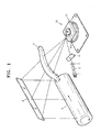
- FIG. 1 is a schematic structural diagram illustrating a light scanning unit, in which a polygonal mirror 11 is used, according to an embodiment of the present general inventive concept.
- FIG. 2 is a schematic perspective view illustrating the polygonal mirror 11 used in the light scanning unit of FIG. 1 , according to an embodiment of the present general inventive concept.
- the light scanning unit includes a light source 1, a polygonal mirror assembly 10 that includes the polygonal mirror 11 and that rotates, and a scanning lens 7.
- the light source 1 emits light beams, and may be, for example, a semiconductor laser diode that emits a laser beam.
- a plurality of light beams may be emitted from the light source 1. Referring to FIG. 1 , one light beam is emitted from the light source 1.
- the plurality of light beams may be incident on one of reflection surfaces 11a of the polygonal mirror 11 at different incident angles or may be incident on different reflection surfaces 11a.
- a collimating lens 2 may be disposed on a light path between the light source 1 and the polygonal mirror 11.
- the collimating lens 2 is a condensing lens that collimates light emitted from the light source 1.
- a cylindrical lens 4 may be further disposed on a light path between the collimating lens 2 and the polygonal mirror 11.
- the cylindrical lens 4 is an optical element having a predetermined power in only a sub-scanning direction, and focuses light that has transmitted through the collimating lens 2 onto the reflection surfaces 11a of the polygonal mirror 11 in a sub-scanning direction.
- an aperture stop 3 may be further disposed between the collimating lens 2 and the cylindrical lens 4 to adjust a diameter of a beam.
- the collimating lens 2, the aperture stop 3, and the cylindrical lens 4 constitute an incident optical system of the light scanning unit.
- the scanning lens 7 is an example of an imaging optical system that has a converging function and f- ⁇ characteristics, and allows each of light beams deflected and scanned by the polygonal mirror 11 to be imaged on an outer surface of a photoconductor 9 at a constant velocity.
- an imaging optical system is constituted by one scanning lens 7, but the imaging optical system may also be constituted by at least two lenses.
- a mirror 8 is an example of a light path changing unit that appropriately changes a path of a scanning light beam.
- the polygonal mirror 11 includes the plurality of reflection surfaces 11 a on its outer portions and an internal mirror surface 11b defining a hole formed in a center portion of the polygonal mirror 11.
- the internal mirror surface 11b of the polygonal mirror 11 and an outer surface of a holder frame 12 ( FIG. 6 ) facing the internal mirror surface 11b are coupled to each other using an adhesive 13 ( FIG. 6 ).
- the polygonal mirror 11 may be formed of a plastic material by using an injection molding method. As the polygonal mirror 11 is formed of a plastic material, the manufacturing costs of the polygonal mirror 11 may be reduced, and also, due to being formed by an injection molding method, mass-production of the polygonal mirror 11 is relatively easy.
- a reflection layer may be formed on the reflection surfaces 11a.
- a metal layer having a relatively good reflectivity such as aluminum (Al) or silver (Ag) may be attached to the reflection surfaces 11 a.
- a protection layer such as SiO 2 may be further formed on an outer surface of the reflection layer in order to protect the reflection layer from external environment and to prevent oxidization of the reflection layer.
- the polygonal mirror 11 may have a quadrangle shape in which the number of the reflection surfaces 11a is four. However, the current embodiment is not limited to the number of reflection surfaces 11a described in the above embodiment.
- An operating temperature range of the light scanning unit is 50 to 60°C, and the polygonal mirror 11 rotates at a relatively high speed of more than 10000 rpm.
- Conventional polygonal mirrors are formed of a metal (e.g., aluminum), and thus when using the conventional polygonal mirrors in the light scanning unit, deformation of the polygonal mirrors due to heat generated in the light scanning unit or centrifugal force generated by high speed rotation is relatively small.
- the polygonal mirror 11 formed of a plastic material has a relatively low Young's Modulus, and thus the reflection surfaces 11a of the polygonal mirror 11 may be deformed in a main scanning direction due to mass thereof, heat, and centrifugal force generated by rotation. The deformation of the reflection surfaces 11a may decrease an overall printing quality due to a decrease in resolution caused by increased beam sizes and irregularities with respect to linearity of beams at various positions of the photoconductor 9 (see FIG. 1 ) in an image forming apparatus.
- the inventors have found that deterioration of optical performance due to deformation of the reflection surfaces 11a caused by heat or high speed rotation may be minimized by limiting dimensions of the polygonal mirror 11 to ranges defined by Inequalities 1 and 2 shown below.
- a diagonal length of the polygonal mirror 11, that is, an outer diameter D, and a diameter corresponding to the internal mirror surface 11b, that is, an internal diameter d may be in the ranges defined by Inequalities 1 and 2 in order to maintain an adhesion force and minimize deformation of the reflection surfaces 11a of the polygonal mirror 11.
- Inequalities 1 and 2 in order to maintain an adhesion force and minimize deformation of the reflection surfaces 11a of the polygonal mirror 11.
- the polygonal mirror 11 may have the outer diameter D being 20 mm and the internal diameter d being 4 mm as given in Table 1.
- the polygonal mirror 11 may be formed of a plastic material having a thermal expansion coefficient ⁇ that satisfies Inequality 3 below: 40 * 10 - 6 1 ⁇ m / m ⁇ °C ⁇ ⁇ ⁇ 400 * 10 - 6 1 ⁇ m / mm ⁇ °C
- the polygonal mirror 11 may have the following properties and be under the following conditions.
- [Table 1] Mirror shape - Four-sided mirror (regular square) - Outer diameter (D): 20mm - Internal diameter (d) : 4mm - Mirror thickness: 2.5mm Young' s Modulus 2.30*10 3 MPa Poisson' s Ratio 0.38 Density 1.20*10 -6 kg/mm 2 Rotational speed 41,000 rpm Temperature 60 L
- FIG. 3 illustrates a deformation of the polygonal mirror 11 having the properties and under the conditions shown in Table 1, by heat and rotation.
- an interval between contours of the reflection surfaces 11a of the polygonal mirror 11 means an elevation difference of 0.05 ⁇ m.
- planarity of the reflection surfaces 11a of the polygonal mirror 11 that directly affects optical characteristics of the polygonal mirror 11 is only about 0.15 ⁇ m, and thus deformation of the reflection surface 11a is not greatly influenced by a temperature increase or a high speed rotation. Since the polygonal mirror 11 is usually controlled to have a tolerance of about 0.2 ⁇ m, the planarity of the polygonal mirror 11 may be within an allowable tolerance.
- planarity may be understood as a deviation of maximums and minimums of deformation of the reflection surfaces 11a in a vertical direction of the reflection surfaces 11 a.
- FIG. 4 illustrates a deformation of a polygonal mirror 11', as a comparative example of the polygonal mirror 11 of FIG. 2 , due to heat and rotation.
- an interval between contours means an elevation difference of 0.05 ⁇ m.
- the polygonal mirror 11' illustrated in FIG. 4 has the properties and is under the conditions shown in Table 1 except that the internal diameter d is 8 mm. Since the internal diameter d is increased, a ratio d/D of the internal diameter d to the outer diameter D is 0.4 and thus the polygonal mirror 11' does not satisfy Inequality 1.
- planarity of the polygonal mirror 11' of the comparative example is 1.65 ⁇ m, which is relatively large. Since the polygonal usually has an allowable tolerance of about 0.2 ⁇ m, deformation of the polygonal mirror 11' of the comparative example is significantly greater than the allowable tolerance and thus has greatly reduced optical performance.
- the polygonal mirror 11" illustrated in FIG. 5 has the properties and is under the conditions shown in Table 1 except that the internal diameter d is 6 mm.
- the ratio d/D of the internal diameter d to the outer diameter D is 0.3 and thus the polygonal mirror 11" does satisfy Inequality 1.
- the interval of the contours of the polygonal mirror 11" is narrower than the interval of the contours of the polygonal mirror 11 of FIG. 3 but much wider than the interval of the contours of the polygonal mirror 11' of FIG. 4 . That is, the polygonal mirror 11" illustrated in FIG. 5 is much more planar than the polygonal mirror 11' of FIG. 4 .
- FIG. 6 illustrates an assembly 10 of the polygonal mirror 11 of FIG. 2 , according to an embodiment of the present general inventive concept.
- the polygonal mirror assembly 10 includes the polygonal mirror 11, the holder frame 12, and a motor unit 14.
- the polygonal mirror 11 is adhered to the holder frame 12 using the adhesive 13.
- the adhesive 13 include a UV-curing adhesive, an instant glue, and a thermosetting adhesive.
- a UV-curing adhesive is used as the adhesive 13
- the internal mirror surface 11b of the polygonal mirror 11 or the outer surface of the holder frame 12 facing the internal surface 11b may be coated with the adhesive 13, and the polygonal mirror 11 and the holder frame 12 are coupled to each other and UV light is irradiated thereon using an UV lamp, thereby quickly solidifying the adhesive 13 to fix the polygonal mirror 11 and the holder frame 12.
- the motor unit 14 includes a bearing holder 18 fixed to a printed circuit board 21, an electromagnet 19 disposed around the bearing holder 18, a shaft 17 that is rotatably installed in the bearing holder 18, a bushing 20 disposed between the bearing holder 18 and the shaft 17, a rotor housing 15 coupled to the shaft 17, and a permanent magnet 16 that is provided inside the rotor housing 15 to face the electromagnet 19.
- Light emitted from the light source 1 is sequentially transmitted through the collimating lens 2, the aperture stop 3, and the cylindrical lens 4, and is irradiated onto and reflected by the reflection surfaces 11 of the polygonal mirror 11.
- the light reflected by the reflection surfaces 11a of the polygonal mirror 11 passes through the scanning lens 7 and is reflected by the mirror 8, and is irradiated onto the outer surface of the photoconductor 9.
- the rotor housing 15 rotates around the shaft 17 due to an electromagnetic interaction between the electromagnet 19 and the permanent magnet 16.
- the holder frame 12 is coupled to the rotor housing 15 and the shaft 17 and rotate together therewith, and here the polygonal mirror 11 coupled to the holder frame 12 also rotates together therewith.
- FIG. 7 illustrates a polygonal mirror 31 according to another embodiment of the present general inventive concept.
- the polygonal mirror 31 further includes a plurality of grooves 31 b in an internal mirror surface 31 a.
- Other parts other than for the plurality of grooves 31 b in the polygonal mirror 31 are substantially the same as the polygonal mirror 11 in the previous embodiment.
- the grooves 31 b are formed in portions of the internal mirror surface 31 a where accumulated masses are relatively large, with respect to a central axis, that is, in directions toward corners of the polygonal mirror 31.
- the grooves 31 b are formed in four corner directions in the internal mirror surface 31 a.
- N grooves 31b may be formed.
- the grooves 31b may be formed to correspond to a vertical length of the polygonal mirror 31.
- An amount that the polygonal mirror 31 deforms when the light scanning unit operates may be determined by functions dependent on a volume, a density, a rotational speed, a form, an elastic coefficient, or a Poisson's ratio of the polygonal mirror 31.
- a difference in the planarity of reflection surfaces is generated by centrifugal force or heat (i.e., temperature change).
- deformation due to centrifugal force is generated more in the corner portions of the polygonal mirror 31 by centrifugal force due to the accumulated mass.
- deformation of the polygonal mirror 31 due to centrifugal force may be reduced by reducing the accumulated mass of the polygonal mirror 31 by using the grooves 31 b formed in directions toward the corners of the polygonal mirror 31.
- the adhesive 13 ( FIG. 6 ) is filled in the plurality of grooves 31 b formed in the internal mirror surface 31a of the polygonal mirror 31 to point-bond the polygonal mirror 31 and the holder frame 12 ( FIG. 6 ).
- the polygonal mirror 31 is a four-sided mirror as illustrated in FIG. 7
- the polygonal mirror 31 and the holder frame 12 are bonded at four points.
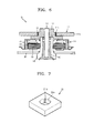
- FIG. 8 illustrates a polygonal mirror 31' according to another embodiment of the present general inventive concept.
- FIG. 9 illustrates an assembly of the polygonal mirror 31' of FIG. 8 .
- the polygonal mirror 31' includes a flow preventing step 31'b formed in an internal mirror surface 31'a.
- Other parts other than for the flow preventing step 31'b in the polygonal mirror 31' are substantially the same as the polygonal mirror 11 in the previous embodiment.
- the flow preventing step 31'b may be formed to a predetermined depth in at least an upper circumferential portion of the internal mirror surface 31'b of the polygonal mirror 31'.
- the flow preventing step 31'b is formed in directions toward corners of the polygonal mirror 31', an accumulated mass of the polygonal mirror 31' is reduced, thereby reducing deformation of the polygonal mirror 31' due to centrifugal force.
- the adhesive 13 ( FIG. 6 ) is filled in the flow preventing step 31'b so as to point-bond the polygonal mirror 31' and the holder frame 12 ( FIG. 6 ).
- the polygonal mirror 31' is a four-sided mirror as illustrated in FIG. 8 , the polygonal mirror 31' and the holder frame 12 are bonded at four points.
- the adhesive 13 may leak out between the polygonal mirror 31' and the holder frame 12 before the adhesive 13 is completely hardened, which might cause the polygonal mirror 31' to be tilted with respect to the holder frame 12.
- the step 31'b prevents the adhesive 13 from leaking out between the polygonal mirror 31' and the holder frame 12 so that the polygonal mirror 31' is properly coupled to the holder frame 12.
- N flow preventing steps 31'b may be provided.
- the internal mirror surfaces 11 b, 31 a, and 31'a that is, holes, of the polygonal mirrors 11, 11', 11", 31, and 31' have a circular cross-section, but are not limited thereto.
- FIG. 10 illustrates a polygonal mirror 41, as another modification example of the polygonal mirror 11 of FIG. 2 .
- the polygonal mirror 41 is a four-sided mirror having four reflection surfaces 41a, and an internal mirror surface 41 b that defines a hole also has four sides, and thus the internal mirror surface 41 b has the same polyhedral shape as the polygonal mirror 41 having four reflection surfaces 41 a.
- Corners of the internal mirror surface 41 b are located in the same directions as corners of the reflection surfaces 41 a. Accordingly, an accumulated mass of the polygonal mirror 41 at the corners of the reflection surfaces 41 a is reduced, and thus deformation of the polygonal mirror 41 due to centrifugal force caused by high speed rotation may be reduced. Furthermore, in a more general way, when the polygonal mirror 41 is an N-sided mirror, the internal mirror surface 41 b may have the same polyhedral shape having N sides as the N-sided mirror.
- FIG. 11 is a structural diagram illustrating an image forming apparatus according to an embodiment of the present general inventive concept, using the light scanning unit according to the previous embodiment of the present general inventive concept.
- the image forming apparatus includes a light scanning unit 100, a plurality of developing units 200, a transfer unit 300, and a fixing unit 400.
- the light scanning unit 100 may be the light scanning unit 100 described above. In order to print a color image, the light scanning unit 100 scans a plurality of light beams, and the plurality of developing units 200, one for each of colors to be printed, may be formed to correspond to the plurality of light beams. In this regard, a plurality of light scanning units 100 each scanning one light beam, may be provided or the light scanning unit 100 may simultaneously scan a plurality of light beams using one polygonal mirror 10 ( FIG. 1 ). For example, the light scanning unit 100 may scan four light beams corresponding to black (K), magenta (M), yellow (Y), and cyan (C), and four developing units 200 for black (K), magenta (M), yellow (Y), and cyan (C) may be formed.
- K black
- M magenta
- Y yellow
- C cyan
- the developing units 200 each include a photosensitive drum 210, that is, an image receptor, on which an electrostatic latent image is formed, and a developing roller 220 for developing the electrostatic latent image.
- the photosensitive drum 210 may be a cylindrical metal pipe having a photosensitive layer that has a predetermined thickness and is formed on an outer circumference of the cylindrical metal pipe. Although not shown herein, a photosensitive belt may be employed as the photoreceptor.
- the outer circumference of the photosensitive drum 210 is a surface that is to be exposed.
- a charge roller 230 is disposed on the outer circumference of the photosensitive drum 210 upstream from a region that is to be exposed to the light scanning unit 100.
- the charge roller 230 is a charging unit that contacts the photosensitive drum 210 and rotates to charge the surface of the photosensitive drum with a uniform charge. A charge bias is applied to the charge roller 230.
- a corona charging unit (not shown) may be used instead of the charge roller 230.
- the developing roller 220 having toner adhered to its outer circumference supplies toner to the photosensitive drum 210.
- a development bias is applied to the developing roller 220 to supply toner to the photosensitive drum 210.
- the developing units 200 may further include a supply roller for allowing toner contained in the developing units 200 to adhere to the developing roller 220, a restriction unit for restricting an amount of the toner adhered to the developing roller 220, and an agitator for transporting the toner contained in each of the developing units 200 to the supply roller and/or the developing roller 220.
- the transfer unit 300 may include a paper transfer belt 310 and four transfer rollers 320.
- the paper transfer belt 310 is arranged to face a region of the outer circumference of the photosensitive drum 210 exposed out of the developing units 200.
- the paper transfer belt 310 circulates by being supported by a plurality of support rollers 330, 340, 350, and 360.
- the four transfer rollers 320 are arranged to face the photosensitive drum 210 of each developing unit 300 with the paper transfer belt 310 interposed therebetween.
- a transfer bias is applied to each of the transfer rollers 320.
- a medium that finally receives the toner image for example, paper P
- paper P is ejected from a cassette 500 by a pickup roller 510.
- the paper P is transferred to the paper transfer belt 310 by a transfer roller 520.
- the paper P adheres to a surface of the paper transfer belt 310 due to an electrostatic force and is transferred at the same velocity as a running linear velocity of the paper transfer belt 310.
- a leading end of the paper P arrives at a transfer nip at the same time as when a leading end of a toner image of cyan (C) formed on the outer circumferential surface of one photosensitive drum 210 of one developing unit 200 arrives at the transfer nip facing the transfer roller 320.
- a transfer bias is applied to the transfer roller 320, the toner image formed on the photosensitive drum 210 is transferred to the paper P.
- toner images of magenta (M), yellow (Y), and black (K) formed on the photosensitive drums 210 of the other developing units 200 are sequentially transferred to the paper P to overlap with one another. Accordingly, a color toner image is formed on the paper P.
- the color toner image transferred to the paper P is maintained on a surface of the paper P due to an electrostatic force.
- the fixing unit 400 fixes the color toner image on the paper P by using heat and pressure.
- the paper P after being subjected to the fixing process is ejected out of the image forming apparatus by an eject roller 530.
- deformation of the polygonal mirror due to heat generated or high speed rotation during an operation may be minimized, thereby minimizing a decrease in performance.
Landscapes
- Physics & Mathematics (AREA)
- Optics & Photonics (AREA)
- General Physics & Mathematics (AREA)
- Facsimile Scanning Arrangements (AREA)
- Mechanical Optical Scanning Systems (AREA)
- Laser Beam Printer (AREA)
Abstract
Description
- The present general inventive concept relates to a polygonal mirror, a light scanning unit using the polygonal mirror, and an image forming apparatus, and more particularly, a polygonal mirror formed of a plastic material, a light scanning unit using the polygonal mirror, and an image forming apparatus.
- A light scanning unit is used in electrophotographic image forming apparatuses such as laser printers, digital photocopiers, facsimiles, etc. The light scanning unit deflects a light beam irradiated from a light source to which an image signal is applied, and scans the light beam in a main scanning direction of an image carrier. Via main scanning by the light scanning unit and sub-scanning by movement of the image carrier, a latent electrostatic image is formed on the image carrier.
- The light scanning unit includes a polygonal mirror assembly that deflects a light beam irradiated from a light source in an appropriate direction. Conventional polygonal mirrors are formed of a high purity aluminum having a purity of 99% or more and by superprecision processing in order to achieve a reflectivity of 85% or higher. However, the manufacturing costs of the polygonal mirror assembly formed of the aluminum described above are high, and production output thereof may be difficult to adjust.
- The present general inventive concept provides a polygonal mirror formed of a plastic material and capable of minimizing a decrease in performance due to heat generated or high speed rotation during an operation, a light scanning unit using the polygonal mirror, and an image forming apparatus having the polygonal mirror.
- According to the present invention there is provided an apparatus and method as set forth in the appended claims. Other features of the invention will be apparent from the dependent claims, and the description which follows.
- According to an aspect of the present general inventive concept, there is provided a polygonal mirror formed of a plastic, wherein the polygonal mirror comprises a plurality of reflection surfaces that are formed on an outer portion of the polygonal mirror and rotate around a rotational axis and an internal mirror surface that defines a hole, and a ratio of an internal diameter d to an outer diameter D satisfies 0.1≤d/D≤0.3.
- The outer diameter D may satisfy 10 mm ≤ D ≤ 30 mm.
- The outer diameter D may be 20 mm and the internal diameter d may be 4 mm.
- A thermal expansion coefficient of the plastic may satisfy 40*10-6 [1m/m·°C] ≤ α ≤ 400*10-6 [1 m/m·°C].
- The polygonal mirror may be assembled by being adhered to a motor unit that supports and rotates the polygonal mirror, using an adhesive, and a groove may be formed in the internal mirror surface to accommodate the adhesive.
- The groove may be formed in a direction toward a corner of the reflection surfaces.
- The groove may be formed to correspond to a vertical length of the internal mirror surface.
- The groove may be formed only in an upper portion of the internal mirror surface.
- The groove may be cylindrical or in the same polyhedral shape as the polygon mirror having the plurality of reflection surfaces.
- A reflection layer may be formed on the plurality of reflection surfaces.
- According to another aspect of the present general inventive concept, there is provided a light scanning unit comprising a light source to emit a light beam; a polygonal mirror to deflect the light beam emitted from the light source, in a main scanning direction; and an imaging optical system to image the light beam deflected by the polygonal mirror, onto a scanning surface, wherein the polygonal mirror is formed of a plastic and comprises a plurality of reflection surfaces that are formed in an outer portion of the polygonal mirror and rotate around a rotational axis and an internal mirror surface that defines a hole, wherein a ratio of an internal diameter d to an outer diameter D satisfies 0.1≤d/D≤0.3.
- The above and other features and advantages of the present general inventive concept will become more apparent by describing in detail exemplary embodiments thereof with reference to the attached drawings in which:
-
FIG. 1 is a schematic structural diagram illustrating a light scanning unit according to an embodiment of the present general inventive concept; -
FIG. 2 is a schematic perspective view illustrating a polygonal mirror used in the light scanning unit ofFIG. 1 , according to an embodiment of the present general inventive concept; -
FIG. 3 illustrates a deformation of the polygonal mirror ofFIG. 2 due to heat and rotation; -
FIG. 4 illustrates a deformation of a comparative example of the polygonal mirror ofFIG. 2 due to heat and rotation; -
FIG. 5 illustrates a deformation of the polygonal mirror ofFIG. 2 , under conditions different from those ofFIG. 3 due to heat and rotation; -
FIG. 6 illustrates an assembly of the polygonal mirror ofFIG. 2 , according to an embodiment of the present general inventive concept; -
FIG. 7 illustrates a polygonal mirror according to another embodiment of the present general inventive concept; -
FIG. 8 illustrates a polygonal mirror according to another embodiment of the present general inventive concept; -
FIG. 9 illustrates an assembly of the polygonal mirror ofFIG. 8 ; -
FIG. 10 illustrates another modification example of the polygonal mirror ofFIG. 2 ; and -
FIG. 11 is a structural diagram illustrating an electrophotographic image forming apparatus according to an embodiment of the present general inventive concept. - The present general inventive concept will now be described more fully with reference to the accompanying drawings, in which exemplary embodiments of the present general inventive concept are shown. Like reference numerals in the drawings denote like elements. In the drawings, the thicknesses of layers and regions are exaggerated for clarity.
-
FIG. 1 is a schematic structural diagram illustrating a light scanning unit, in which apolygonal mirror 11 is used, according to an embodiment of the present general inventive concept.FIG. 2 is a schematic perspective view illustrating thepolygonal mirror 11 used in the light scanning unit ofFIG. 1 , according to an embodiment of the present general inventive concept. - Referring to
FIG. 1 , the light scanning unit includes a light source 1, apolygonal mirror assembly 10 that includes thepolygonal mirror 11 and that rotates, and ascanning lens 7. - The light source 1 emits light beams, and may be, for example, a semiconductor laser diode that emits a laser beam. A plurality of light beams may be emitted from the light source 1. Referring to
FIG. 1 , one light beam is emitted from the light source 1. When a plurality of light beams are emitted from the light source 1, the plurality of light beams may be incident on one ofreflection surfaces 11a of thepolygonal mirror 11 at different incident angles or may be incident ondifferent reflection surfaces 11a. - A collimating
lens 2 may be disposed on a light path between the light source 1 and thepolygonal mirror 11. The collimatinglens 2 is a condensing lens that collimates light emitted from the light source 1. A cylindrical lens 4 may be further disposed on a light path between thecollimating lens 2 and thepolygonal mirror 11. The cylindrical lens 4 is an optical element having a predetermined power in only a sub-scanning direction, and focuses light that has transmitted through thecollimating lens 2 onto thereflection surfaces 11a of thepolygonal mirror 11 in a sub-scanning direction. Also, an aperture stop 3 may be further disposed between the collimatinglens 2 and the cylindrical lens 4 to adjust a diameter of a beam. Thecollimating lens 2, the aperture stop 3, and the cylindrical lens 4 constitute an incident optical system of the light scanning unit. - The
scanning lens 7 is an example of an imaging optical system that has a converging function and f-θ characteristics, and allows each of light beams deflected and scanned by thepolygonal mirror 11 to be imaged on an outer surface of a photoconductor 9 at a constant velocity. Referring toFIG. 1 , an imaging optical system is constituted by onescanning lens 7, but the imaging optical system may also be constituted by at least two lenses. Amirror 8 is an example of a light path changing unit that appropriately changes a path of a scanning light beam. - Referring to
FIG. 2 , thepolygonal mirror 11 includes the plurality ofreflection surfaces 11 a on its outer portions and aninternal mirror surface 11b defining a hole formed in a center portion of thepolygonal mirror 11. Theinternal mirror surface 11b of thepolygonal mirror 11 and an outer surface of a holder frame 12 (FIG. 6 ) facing theinternal mirror surface 11b are coupled to each other using an adhesive 13 (FIG. 6 ). Thepolygonal mirror 11 may be formed of a plastic material by using an injection molding method. As thepolygonal mirror 11 is formed of a plastic material, the manufacturing costs of thepolygonal mirror 11 may be reduced, and also, due to being formed by an injection molding method, mass-production of thepolygonal mirror 11 is relatively easy. A reflection layer may be formed on the reflection surfaces 11a. For example, a metal layer having a relatively good reflectivity, such as aluminum (Al) or silver (Ag), may be attached to the reflection surfaces 11 a. A protection layer such as SiO2 may be further formed on an outer surface of the reflection layer in order to protect the reflection layer from external environment and to prevent oxidization of the reflection layer. Thepolygonal mirror 11 may have a quadrangle shape in which the number of thereflection surfaces 11a is four. However, the current embodiment is not limited to the number ofreflection surfaces 11a described in the above embodiment. - An operating temperature range of the light scanning unit is 50 to 60°C, and the
polygonal mirror 11 rotates at a relatively high speed of more than 10000 rpm. Conventional polygonal mirrors are formed of a metal (e.g., aluminum), and thus when using the conventional polygonal mirrors in the light scanning unit, deformation of the polygonal mirrors due to heat generated in the light scanning unit or centrifugal force generated by high speed rotation is relatively small. However, thepolygonal mirror 11 formed of a plastic material has a relatively low Young's Modulus, and thus the reflection surfaces 11a of thepolygonal mirror 11 may be deformed in a main scanning direction due to mass thereof, heat, and centrifugal force generated by rotation. The deformation of the reflection surfaces 11a may decrease an overall printing quality due to a decrease in resolution caused by increased beam sizes and irregularities with respect to linearity of beams at various positions of the photoconductor 9 (seeFIG. 1 ) in an image forming apparatus. - Thus, the inventors have found that deterioration of optical performance due to deformation of the reflection surfaces 11a caused by heat or high speed rotation may be minimized by limiting dimensions of the
polygonal mirror 11 to ranges defined byInequalities 1 and 2 shown below. - That is, a diagonal length of the
polygonal mirror 11, that is, an outer diameter D, and a diameter corresponding to theinternal mirror surface 11b, that is, an internal diameter d, may be in the ranges defined byInequalities 1 and 2 in order to maintain an adhesion force and minimize deformation of the reflection surfaces 11a of thepolygonal mirror 11.

- For example, the
polygonal mirror 11 may have the outer diameter D being 20 mm and the internal diameter d being 4 mm as given in Table 1. - In addition, the
polygonal mirror 11 may be formed of a plastic material having a thermal expansion coefficient α that satisfies Inequality 3 below:
- For example, the
polygonal mirror 11 may be formed of a plastic material such as cyclic olefin copolymer (COC), poly carbonate (PC), polymethyl methacrylate (PMMA), or cyclo-olefin polymer (COP), so as to satisfy the condition of Inequality 3. - Hereinafter, a deformation of the
polygonal mirror 11 due to heat and rotation when the above conditions are met and when the above conditions are not met will be described with reference to examples. - For example, the
polygonal mirror 11 according to the current embodiment may have the following properties and be under the following conditions.[Table 1] Mirror shape - Four-sided mirror (regular square) - Outer diameter (D): 20mm - Internal diameter (d) : 4mm - Mirror thickness: 2.5mm Young' s Modulus 2.30*103 MPa Poisson' s Ratio 0.38 Density 1.20*10-6 kg/mm2 Rotational speed 41,000 rpm Temperature 60 L -
FIG. 3 illustrates a deformation of thepolygonal mirror 11 having the properties and under the conditions shown in Table 1, by heat and rotation. InFIG. 3 , an interval between contours of the reflection surfaces 11a of thepolygonal mirror 11 means an elevation difference of 0.05 µm. Referring toFIG. 3 , planarity of the reflection surfaces 11a of thepolygonal mirror 11 that directly affects optical characteristics of thepolygonal mirror 11 is only about 0.15 µm, and thus deformation of thereflection surface 11a is not greatly influenced by a temperature increase or a high speed rotation. Since thepolygonal mirror 11 is usually controlled to have a tolerance of about 0.2 µm, the planarity of thepolygonal mirror 11 may be within an allowable tolerance. Here, planarity may be understood as a deviation of maximums and minimums of deformation of the reflection surfaces 11a in a vertical direction of the reflection surfaces 11 a. -
FIG. 4 illustrates a deformation of a polygonal mirror 11', as a comparative example of thepolygonal mirror 11 ofFIG. 2 , due to heat and rotation. InFIG. 4 , an interval between contours means an elevation difference of 0.05 µm. - The polygonal mirror 11' illustrated in
FIG. 4 has the properties and is under the conditions shown in Table 1 except that the internal diameter d is 8 mm. Since the internal diameter d is increased, a ratio d/D of the internal diameter d to the outer diameter D is 0.4 and thus the polygonal mirror 11' does not satisfy Inequality 1. Referring toFIG. 4 , planarity of the polygonal mirror 11' of the comparative example is 1.65 µm, which is relatively large. Since the polygonal usually has an allowable tolerance of about 0.2 µm, deformation of the polygonal mirror 11' of the comparative example is significantly greater than the allowable tolerance and thus has greatly reduced optical performance. -
FIG. 5 illustrates a deformation of apolygonal mirror 11 ", as another example of thepolygonal mirror 11 ofFIG. 2 , due to heat and rotation, under conditions different from those ofFIG. 3 . InFIG. 5 , an interval between contours means an elevation difference of 0.05 µm. - The
polygonal mirror 11" illustrated inFIG. 5 has the properties and is under the conditions shown in Table 1 except that the internal diameter d is 6 mm. The ratio d/D of the internal diameter d to the outer diameter D is 0.3 and thus thepolygonal mirror 11" does satisfy Inequality 1. Referring toFIG. 5 , the interval of the contours of thepolygonal mirror 11" is narrower than the interval of the contours of thepolygonal mirror 11 ofFIG. 3 but much wider than the interval of the contours of the polygonal mirror 11' ofFIG. 4 . That is, thepolygonal mirror 11" illustrated inFIG. 5 is much more planar than the polygonal mirror 11' ofFIG. 4 . - Next, an assembly of the
polygonal mirror 11 will be described.FIG. 6 illustrates anassembly 10 of thepolygonal mirror 11 ofFIG. 2 , according to an embodiment of the present general inventive concept. Referring toFIG. 6 , thepolygonal mirror assembly 10 includes thepolygonal mirror 11, theholder frame 12, and amotor unit 14. - The
polygonal mirror 11 is adhered to theholder frame 12 using the adhesive 13. Examples of the adhesive 13 include a UV-curing adhesive, an instant glue, and a thermosetting adhesive. For example, when a UV-curing adhesive is used as the adhesive 13, theinternal mirror surface 11b of thepolygonal mirror 11 or the outer surface of theholder frame 12 facing theinternal surface 11b may be coated with the adhesive 13, and thepolygonal mirror 11 and theholder frame 12 are coupled to each other and UV light is irradiated thereon using an UV lamp, thereby quickly solidifying the adhesive 13 to fix thepolygonal mirror 11 and theholder frame 12. - The
motor unit 14 includes abearing holder 18 fixed to a printedcircuit board 21, anelectromagnet 19 disposed around the bearingholder 18, ashaft 17 that is rotatably installed in thebearing holder 18, abushing 20 disposed between the bearingholder 18 and theshaft 17, arotor housing 15 coupled to theshaft 17, and a permanent magnet 16 that is provided inside therotor housing 15 to face theelectromagnet 19. - In conventional polygonal mirror assemblies, a polygonal mirror is fixed to a holder frame (or motor unit) using a plate spring. Although the plate spring causes deformation to the polygonal mirror by elastic force, since conventional polygonal mirrors are formed of a metal such as aluminum, deformation due to the plate spring may be negligible. However, when the
polygonal mirror 11 is formed of a plastic, assembling using a plate spring as described above may cause significant deformation to thepolygonal mirror 11. That is, a polygonal mirror formed of a metal is not greatly deformed even when being assembled by spring pressurization because the Young's modulus thereof is relatively large, and accordingly it is difficult to apply the assembling method of the conventional polygonal mirror formed of a metal to the polygonal mirror formed of a plastic material. Thus, by coupling thepolygonal mirror 11 to theholder frame 12 using the adhesive 13 according to the current embodiment as described above, stress applied to thepolygonal mirror 11 during assembling may be minimized. As such, deformation of the reflection surfaces 11a of thepolygonal mirror 11 is minimized by minimizing the assembling stress, thereby preventing a decrease in performance of the light scanning unit. - While deformation of the
reflection surfaces 11a is significantly reduced by using the adhesive 13, the reflection surfaces 11a may still be deformed by contraction of the adhesive 13. Thus, if the adhesive 13 is unevenly coated on either an upper or lower portion of theinternal mirror surface 11b of thepolygonal mirror 11, portions of thepolygonal mirror 11 are deformed more. Thus, in order to provide uniform deformation distribution, the adhesive 13 is uniformly coated on theinternal mirror surface 11b of thepolygonal mirror 11 or on the outer surface of theholder frame 12 facing theinternal mirror surface 11 b. - Meanwhile, the
polygonal mirror 11 according to the current embodiment is coupled to themotor unit 14 via theholder frame 12, but is not limited thereto. Theholder frame 12 may be omitted and theshaft 17 of themotor unit 14 may be coupled directly to thepolygonal mirror 11 using the adhesive 13. - Hereinafter, an operation of the light scanning unit according to the current embodiment of the present general inventive concept will be described with reference to
FIGS. 1 and2 . - Light emitted from the light source 1 is sequentially transmitted through the
collimating lens 2, the aperture stop 3, and the cylindrical lens 4, and is irradiated onto and reflected by the reflection surfaces 11 of thepolygonal mirror 11. The light reflected by the reflection surfaces 11a of thepolygonal mirror 11 passes through thescanning lens 7 and is reflected by themirror 8, and is irradiated onto the outer surface of the photoconductor 9. When power is applied to theelectromagnet 19 of themotor unit 14, therotor housing 15 rotates around theshaft 17 due to an electromagnetic interaction between theelectromagnet 19 and the permanent magnet 16. Theholder frame 12 is coupled to therotor housing 15 and theshaft 17 and rotate together therewith, and here thepolygonal mirror 11 coupled to theholder frame 12 also rotates together therewith. When thepolygonal mirror 11 is rotated by being driven by themotor unit 14 as described above, light reflected by the reflection surfaces 11a of thepolygonal mirror 11 is scanned in a direction perpendicular to a rotational axis of thepolygonal mirror 11, that is, in a main scanning direction. Meanwhile, the photoconductor 9 shifts a scanning surface in a direction perpendicular to a direction in which light is scanned by thepolygonal mirror 11. Accordingly, by turning on and off the light source 1, an electrostatic latent image formed of a combination of exposed portions and non-exposed portions is formed on the outer surface of the photoconductor 9. -
FIG. 7 illustrates apolygonal mirror 31 according to another embodiment of the present general inventive concept. Referring toFIG. 7 , thepolygonal mirror 31 further includes a plurality ofgrooves 31 b in aninternal mirror surface 31 a. Other parts other than for the plurality ofgrooves 31 b in thepolygonal mirror 31 are substantially the same as thepolygonal mirror 11 in the previous embodiment. Thegrooves 31 b are formed in portions of theinternal mirror surface 31 a where accumulated masses are relatively large, with respect to a central axis, that is, in directions toward corners of thepolygonal mirror 31. For example, when thepolygonal mirror 31 is a four-sided mirror as illustrated inFIG. 7 , thegrooves 31 b are formed in four corner directions in theinternal mirror surface 31 a. When thepolygonal mirror 31 has N reflection surfaces,N grooves 31b may be formed. Thegrooves 31b may be formed to correspond to a vertical length of thepolygonal mirror 31. - An amount that the
polygonal mirror 31 deforms when the light scanning unit operates may be determined by functions dependent on a volume, a density, a rotational speed, a form, an elastic coefficient, or a Poisson's ratio of thepolygonal mirror 31. When considering data of the deformation shown inFIGS. 3 through 5 , a difference in the planarity of reflection surfaces is generated by centrifugal force or heat (i.e., temperature change). For example, deformation due to centrifugal force is generated more in the corner portions of thepolygonal mirror 31 by centrifugal force due to the accumulated mass. However, according to the current embodiment, deformation of thepolygonal mirror 31 due to centrifugal force may be reduced by reducing the accumulated mass of thepolygonal mirror 31 by using thegrooves 31 b formed in directions toward the corners of thepolygonal mirror 31. - The adhesive 13 (
FIG. 6 ) is filled in the plurality ofgrooves 31 b formed in theinternal mirror surface 31a of thepolygonal mirror 31 to point-bond thepolygonal mirror 31 and the holder frame 12 (FIG. 6 ). For example, when thepolygonal mirror 31 is a four-sided mirror as illustrated inFIG. 7 , thepolygonal mirror 31 and theholder frame 12 are bonded at four points. -
FIG. 8 illustrates a polygonal mirror 31' according to another embodiment of the present general inventive concept.FIG. 9 illustrates an assembly of the polygonal mirror 31' ofFIG. 8 . Referring toFIGS. 8 and 9 , the polygonal mirror 31' includes a flow preventing step 31'b formed in an internal mirror surface 31'a. Other parts other than for the flow preventing step 31'b in the polygonal mirror 31' are substantially the same as thepolygonal mirror 11 in the previous embodiment. The flow preventing step 31'b may be formed to a predetermined depth in at least an upper circumferential portion of the internal mirror surface 31'b of the polygonal mirror 31'. Like thegrooves 31 b described above with reference toFIG. 7 , since the flow preventing step 31'b is formed in directions toward corners of the polygonal mirror 31', an accumulated mass of the polygonal mirror 31' is reduced, thereby reducing deformation of the polygonal mirror 31' due to centrifugal force. Also, the adhesive 13 (FIG. 6 ) is filled in the flow preventing step 31'b so as to point-bond the polygonal mirror 31' and the holder frame 12 (FIG. 6 ). For example, when the polygonal mirror 31' is a four-sided mirror as illustrated inFIG. 8 , the polygonal mirror 31' and theholder frame 12 are bonded at four points. When the bonding is performed using the adhesive 13, the adhesive 13 may leak out between the polygonal mirror 31' and theholder frame 12 before the adhesive 13 is completely hardened, which might cause the polygonal mirror 31' to be tilted with respect to theholder frame 12. Thus, the step 31'b prevents the adhesive 13 from leaking out between the polygonal mirror 31' and theholder frame 12 so that the polygonal mirror 31' is properly coupled to theholder frame 12. Like in the above-described example, when the polygonal mirror 31' has N reflection surfaces, N flow preventing steps 31'b may be provided. - In the above-described embodiments, the internal mirror surfaces 11 b, 31 a, and 31'a, that is, holes, of the polygonal mirrors 11, 11', 11", 31, and 31' have a circular cross-section, but are not limited thereto. For example,
FIG. 10 illustrates apolygonal mirror 41, as another modification example of thepolygonal mirror 11 ofFIG. 2 . Referring toFIG. 10 , thepolygonal mirror 41 is a four-sided mirror having fourreflection surfaces 41a, and aninternal mirror surface 41 b that defines a hole also has four sides, and thus theinternal mirror surface 41 b has the same polyhedral shape as thepolygonal mirror 41 having fourreflection surfaces 41 a. Corners of theinternal mirror surface 41 b are located in the same directions as corners of the reflection surfaces 41 a. Accordingly, an accumulated mass of thepolygonal mirror 41 at the corners of the reflection surfaces 41 a is reduced, and thus deformation of thepolygonal mirror 41 due to centrifugal force caused by high speed rotation may be reduced. Furthermore, in a more general way, when thepolygonal mirror 41 is an N-sided mirror, theinternal mirror surface 41 b may have the same polyhedral shape having N sides as the N-sided mirror. -
FIG. 11 is a structural diagram illustrating an image forming apparatus according to an embodiment of the present general inventive concept, using the light scanning unit according to the previous embodiment of the present general inventive concept. - The image forming apparatus is a dry type electrophotographic image forming apparatus for printing a color image using a dry developer (hereinafter referred to as a toner).
- Referring to
FIG. 11 , the image forming apparatus includes alight scanning unit 100, a plurality of developingunits 200, atransfer unit 300, and a fixing unit 400. - The
light scanning unit 100 may be thelight scanning unit 100 described above. In order to print a color image, thelight scanning unit 100 scans a plurality of light beams, and the plurality of developingunits 200, one for each of colors to be printed, may be formed to correspond to the plurality of light beams. In this regard, a plurality oflight scanning units 100 each scanning one light beam, may be provided or thelight scanning unit 100 may simultaneously scan a plurality of light beams using one polygonal mirror 10 (FIG. 1 ). For example, thelight scanning unit 100 may scan four light beams corresponding to black (K), magenta (M), yellow (Y), and cyan (C), and four developingunits 200 for black (K), magenta (M), yellow (Y), and cyan (C) may be formed. - The developing
units 200 each include a photosensitive drum 210, that is, an image receptor, on which an electrostatic latent image is formed, and a developingroller 220 for developing the electrostatic latent image. - The photosensitive drum 210, that is, a photoreceptor, may be a cylindrical metal pipe having a photosensitive layer that has a predetermined thickness and is formed on an outer circumference of the cylindrical metal pipe. Although not shown herein, a photosensitive belt may be employed as the photoreceptor. The outer circumference of the photosensitive drum 210 is a surface that is to be exposed. A
charge roller 230 is disposed on the outer circumference of the photosensitive drum 210 upstream from a region that is to be exposed to thelight scanning unit 100. Thecharge roller 230 is a charging unit that contacts the photosensitive drum 210 and rotates to charge the surface of the photosensitive drum with a uniform charge. A charge bias is applied to thecharge roller 230. A corona charging unit (not shown) may be used instead of thecharge roller 230. - The developing
roller 220 having toner adhered to its outer circumference supplies toner to the photosensitive drum 210. A development bias is applied to the developingroller 220 to supply toner to the photosensitive drum 210. Although it is not illustrated in the drawings, the developingunits 200 may further include a supply roller for allowing toner contained in the developingunits 200 to adhere to the developingroller 220, a restriction unit for restricting an amount of the toner adhered to the developingroller 220, and an agitator for transporting the toner contained in each of the developingunits 200 to the supply roller and/or the developingroller 220. - The
transfer unit 300 may include apaper transfer belt 310 and four transfer rollers 320. Thepaper transfer belt 310 is arranged to face a region of the outer circumference of the photosensitive drum 210 exposed out of the developingunits 200. Thepaper transfer belt 310 circulates by being supported by a plurality ofsupport rollers unit 300 with thepaper transfer belt 310 interposed therebetween. A transfer bias is applied to each of the transfer rollers 320. - A color image forming process that may be performed by the electrophotographic image forming apparatus configured as above will now be described.
- The photosensitive drum 210 of the developing
units 200 is charged to a uniform electric potential by a charge bias applied to the chargingroller 230. Thelight scanning unit 100 scans four light beams corresponding to image information about cyan (C), magenta (M), yellow (Y), and black (K) colors to each photosensitive drum 210 of the developingunits 200 to form an electrostatic latent image. A development bias is applied to the developingroller 220. Then, toner adhered to the outer circumference of the developingroller 220 adheres to the electrostatic latent image on the photosensitive drum 210 so that toner images of cyan, magenta, yellow, and black may be respectively formed on the photosensitive drum 210 of the developingunit 200. - A medium that finally receives the toner image, for example, paper P, is ejected from a
cassette 500 by apickup roller 510. The paper P is transferred to thepaper transfer belt 310 by atransfer roller 520. The paper P adheres to a surface of thepaper transfer belt 310 due to an electrostatic force and is transferred at the same velocity as a running linear velocity of thepaper transfer belt 310. - For example, a leading end of the paper P arrives at a transfer nip at the same time as when a leading end of a toner image of cyan (C) formed on the outer circumferential surface of one photosensitive drum 210 of one developing
unit 200 arrives at the transfer nip facing the transfer roller 320. When a transfer bias is applied to the transfer roller 320, the toner image formed on the photosensitive drum 210 is transferred to the paper P. As the paper P is transferred, toner images of magenta (M), yellow (Y), and black (K) formed on the photosensitive drums 210 of the other developingunits 200 are sequentially transferred to the paper P to overlap with one another. Accordingly, a color toner image is formed on the paper P. - The color toner image transferred to the paper P is maintained on a surface of the paper P due to an electrostatic force. The fixing unit 400 fixes the color toner image on the paper P by using heat and pressure. The paper P after being subjected to the fixing process is ejected out of the image forming apparatus by an
eject roller 530. - According to the polygonal mirror, the light scanning unit using the polygonal mirror, and the image forming apparatus according to the embodiments of the present general inventive concept, deformation of the polygonal mirror due to heat generated or high speed rotation during an operation may be minimized, thereby minimizing a decrease in performance.
- While the present general inventive concept has been particularly shown and described with reference to exemplary embodiments thereof, it will be understood by those of ordinary skill in the art that various changes in form and details may be made therein without departing from the scope of the present general inventive concept as defined by the following claims.
- Attention is directed to all papers and documents which are filed concurrently with or previous to this specification in connection with this application and which are open to public inspection with this specification, and the contents of all such papers and documents are incorporated herein by reference.
- All of the features disclosed in this specification (including any accompanying claims, abstract and drawings), and/or all of the steps of any method or process so disclosed, may be combined in any combination, except combinations where at least some of such features and/or steps are mutually exclusive.
- Each feature disclosed in this specification (including any accompanying claims, abstract and drawings) may be replaced by alternative features serving the same, equivalent or similar purpose, unless expressly stated otherwise. Thus, unless expressly stated otherwise, each feature disclosed is one example only of a generic series of equivalent or similar features.
- The invention is not restricted to the details of the foregoing embodiment(s). The invention extends to any novel one, or any novel combination, of the features disclosed in this specification (including any accompanying claims, abstract and drawings), or to any novel one, or any novel combination, of the steps of any method or process so disclosed.
Claims (15)
- A polygonal mirror formed of a plastic, wherein the polygonal mirror comprises a plurality of reflection surfaces that are formed on an outer portion of the polygonal mirror and rotate around a rotational axis and an internal mirror surface that defines a hole, and a ratio of an internal diameter d to an outer diameter D satisfies 0.1≤d/D≤0.3.
- The polygonal mirror of claim 1, wherein the outer diameter D satisfies 10 mm ≤ D ≤ 30 mm.
- The polygonal mirror of claim 2, wherein the outer diameter D is 20 mm and the internal diameter d is 4 mm.
- The polygonal mirror of one of claims 1 to 3, wherein a thermal expansion coefficient of the plastic satisfies 40*10-6 [1m/m·°C] ≤ α ≤ 400*10-6 [1 m/m·°C].
- The polygonal mirror of one of claims 1 to 4, wherein the polygonal mirror is assembled by being adhered to a motor unit that supports and rotates the polygonal mirror, using an adhesive, and
a groove is formed in the internal mirror surface to accommodate the adhesive. - The polygonal mirror of claim 5, wherein the groove is formed in a direction toward a corner of the reflection surfaces.
- The polygonal mirror of claim 5 or 6, wherein the groove is formed to correspond to a vertical length of the internal mirror surface.
- The polygonal mirror of claim 5 or 6, wherein the groove is formed only in an upper portion of the internal mirror surface.
- The polygonal mirror of one of claims 5 through 8, wherein the groove is cylindrical or in the same polyhedral shape as the polygon mirror having the plurality of reflection surfaces.
- The polygonal mirror of one of claims 1 to 9, wherein a reflection layer is formed on the plurality of reflection surfaces.
- A light scanning unit comprising:a light source to emit a light beam;a polygonal mirror of one of claims 1 to 10 for deflecting the light beam emitted from the light source, in a main scanning direction; andan imaging optical system to image the light beam deflected by the polygonal mirror, onto a scanning surface,.
- The light scanning unit of claim 11, wherein the polygonal mirror is assembled by being adhered to a motor unit that supports and rotates the polygonal mirror, using an adhesive.
- The light scanning unit of claim 12, wherein a holder frame is coupled to a rotational axis of the motor unit, and a portion of the holder frame is inserted into the hole of the polygonal mirror, and the internal mirror surface of the polygonal mirror defining the hole and an outer surface of the holder frame facing the internal mirror surface are point-bonded using the adhesive.
- The light scanning unit of claim 13, wherein the point-bonding is conducted in a direction toward a corner of the reflection surfaces.
- An image forming apparatus comprising:a light scanning unit of one of claims 11 to 14;a developing unit comprising a photoconductor that is disposed at an imaging point of the light beam emitted from the light scanning unit, wherein an electrostatic latent image is formed on the photoconductor, and a developing roller that develops the electrostatic latent image formed on the photoconductor; anda transfer unit onto which an image developed by the developing unit is transferred.
Applications Claiming Priority (1)
| Application Number | Priority Date | Filing Date | Title |
|---|---|---|---|
| KR1020100122006A KR20120060481A (en) | 2010-12-02 | 2010-12-02 | Polygonal mirror, light scanning unit employing the polygonal mirror and image forming apparatus |
Publications (2)
| Publication Number | Publication Date |
|---|---|
| EP2461191A1 true EP2461191A1 (en) | 2012-06-06 |
| EP2461191B1 EP2461191B1 (en) | 2021-03-31 |
Family
ID=44897636
Family Applications (1)
| Application Number | Title | Priority Date | Filing Date |
|---|---|---|---|
| EP11186429.4A Active EP2461191B1 (en) | 2010-12-02 | 2011-10-25 | Polygonal Mirror, Light Scanning Unit using the Polygonal Mirror, and Image Forming Apparatus |
Country Status (5)
| Country | Link |
|---|---|
| US (2) | US8711196B2 (en) |
| EP (1) | EP2461191B1 (en) |
| JP (1) | JP2012118532A (en) |
| KR (1) | KR20120060481A (en) |
| CN (1) | CN102486547B (en) |
Families Citing this family (11)
| Publication number | Priority date | Publication date | Assignee | Title |
|---|---|---|---|---|
| JP4880302B2 (en) | 2005-12-26 | 2012-02-22 | 株式会社リコー | Optical deflector, optical scanning device, and image forming apparatus |
| KR20120060481A (en) * | 2010-12-02 | 2012-06-12 | 삼성전자주식회사 | Polygonal mirror, light scanning unit employing the polygonal mirror and image forming apparatus |
| JP6364803B2 (en) * | 2014-02-12 | 2018-08-01 | ブラザー工業株式会社 | Polygon mirror, optical scanning device, image forming apparatus, and polygon mirror manufacturing method |
| JP6525557B2 (en) * | 2014-11-12 | 2019-06-05 | キヤノン株式会社 | Optical deflector, scanning optical device and image forming apparatus |
| JP2016180891A (en) | 2015-03-24 | 2016-10-13 | ブラザー工業株式会社 | Optical deflection device |
| JP2017126008A (en) * | 2016-01-15 | 2017-07-20 | ブラザー工業株式会社 | Polygon mirror, polygon mirror manufacturing method, image forming apparatus, and reflection mirror |
| JP6949665B2 (en) * | 2017-10-31 | 2021-10-13 | キヤノン株式会社 | Optical deflector, optical scanning device and image forming device |
| JP2019191334A (en) * | 2018-04-24 | 2019-10-31 | キヤノン株式会社 | Polygon mirror, deflector, optical scanner, image formation device and method for manufacturing polygon mirror |
| CN113552661B (en) * | 2020-04-01 | 2023-12-01 | 宁波舜宇车载光学技术有限公司 | Polygonal prism, laser radar including the same, and method of manufacturing the same |
| JP2023128333A (en) * | 2022-03-03 | 2023-09-14 | キヤノン株式会社 | Polygon mirrors, optical polarizers, optical scanning devices, and image forming devices |
| CN118426167B (en) * | 2024-07-04 | 2024-10-25 | 宁波舜宇车载光学技术有限公司 | Scanning prism module, electronic equipment and motor vehicle with same |
Citations (3)
| Publication number | Priority date | Publication date | Assignee | Title |
|---|---|---|---|---|
| US5124830A (en) * | 1989-12-07 | 1992-06-23 | Kabushiki Kaisha Toshiba | Optical deflector device for deflecting laser beam |
| JPH06110002A (en) * | 1992-09-28 | 1994-04-22 | Canon Inc | Plastic rotating polygon mirror |
| JPH08190067A (en) * | 1995-01-12 | 1996-07-23 | Fuji Xerox Co Ltd | Plastic molded goods for polyhedral mirror |
Family Cites Families (10)
| Publication number | Priority date | Publication date | Assignee | Title |
|---|---|---|---|---|
| JP3312694B2 (en) * | 2000-04-21 | 2002-08-12 | セイコーインスツルメンツ株式会社 | Polygon mirror fixing method and polygon scanner motor |
| JP2006039163A (en) * | 2004-07-27 | 2006-02-09 | Matsushita Electric Ind Co Ltd | Polygon mirror scanner motor |
| JP2006058640A (en) * | 2004-08-20 | 2006-03-02 | Victor Co Of Japan Ltd | Polygon mirror driving motor |
| JP2006251134A (en) * | 2005-03-09 | 2006-09-21 | Matsushita Electric Ind Co Ltd | Polygon mirror |
| JP4880302B2 (en) * | 2005-12-26 | 2012-02-22 | 株式会社リコー | Optical deflector, optical scanning device, and image forming apparatus |
| KR101080415B1 (en) | 2006-06-21 | 2011-11-07 | 삼성전자주식회사 | Light scanning unit and electrophotographic image forming apparatus adopting the same |
| KR20080088222A (en) | 2007-03-29 | 2008-10-02 | 삼성전자주식회사 | Image forming apparatus and optical reflector and polygon mirror |
| JP5151443B2 (en) | 2007-12-13 | 2013-02-27 | 株式会社リコー | Optical scanning device, optical scanning method, and image forming apparatus |
| KR101047226B1 (en) * | 2009-07-06 | 2011-07-06 | 엄용남 | Scanner motor |
| KR20120060481A (en) * | 2010-12-02 | 2012-06-12 | 삼성전자주식회사 | Polygonal mirror, light scanning unit employing the polygonal mirror and image forming apparatus |
-
2010
- 2010-12-02 KR KR1020100122006A patent/KR20120060481A/en not_active Ceased
-
2011
- 2011-10-25 EP EP11186429.4A patent/EP2461191B1/en active Active
- 2011-11-04 US US13/373,093 patent/US8711196B2/en active Active
- 2011-12-02 CN CN201110396352.XA patent/CN102486547B/en active Active
- 2011-12-02 JP JP2011264558A patent/JP2012118532A/en active Pending
-
2014
- 2014-03-14 US US14/211,761 patent/US9429748B2/en active Active
Patent Citations (3)
| Publication number | Priority date | Publication date | Assignee | Title |
|---|---|---|---|---|
| US5124830A (en) * | 1989-12-07 | 1992-06-23 | Kabushiki Kaisha Toshiba | Optical deflector device for deflecting laser beam |
| JPH06110002A (en) * | 1992-09-28 | 1994-04-22 | Canon Inc | Plastic rotating polygon mirror |
| JPH08190067A (en) * | 1995-01-12 | 1996-07-23 | Fuji Xerox Co Ltd | Plastic molded goods for polyhedral mirror |
Also Published As
| Publication number | Publication date |
|---|---|
| CN102486547A (en) | 2012-06-06 |
| US20140198171A1 (en) | 2014-07-17 |
| KR20120060481A (en) | 2012-06-12 |
| US20120141167A1 (en) | 2012-06-07 |
| US8711196B2 (en) | 2014-04-29 |
| JP2012118532A (en) | 2012-06-21 |
| EP2461191B1 (en) | 2021-03-31 |
| CN102486547B (en) | 2016-02-03 |
| US9429748B2 (en) | 2016-08-30 |
Similar Documents
| Publication | Publication Date | Title |
|---|---|---|
| EP2461191B1 (en) | Polygonal Mirror, Light Scanning Unit using the Polygonal Mirror, and Image Forming Apparatus | |
| EP2458414B1 (en) | Polygon mirror assembly, light scanning unit employing polygon mirror assembly, and image forming apparatus | |
| KR101720773B1 (en) | Rotational polygon mirror and light scanning unit employing the same | |
| US8754918B2 (en) | Optical scanner and image forming apparatus including same | |
| US7446917B2 (en) | Optical scanning apparatus | |
| US7830574B2 (en) | Light scanning apparatus | |
| US20090153933A1 (en) | Optical scanning device and image forming apparatus | |
| JP2008216911A (en) | Optical scanning device and image forming device | |
| JP5205791B2 (en) | Optical apparatus and image forming apparatus | |
| US20120269551A1 (en) | Optical scanning apparatus and image forming apparatus including optical scanning apparatus | |
| CN101276177A (en) | Optical unit, imaging device and optical element of the optical unit | |
| CN100454081C (en) | Optical scanning device and image forming device | |
| US8717640B2 (en) | Optical scanner and image forming apparatus including same | |
| JP2013109312A (en) | Optical scanner and image forming apparatus | |
| JP2007047748A (en) | Optical scanning apparatus and image forming apparatus | |
| JP2004102006A (en) | Polygon motor unit, scanning optical device and image forming apparatus using the same | |
| JPH10288747A (en) | Deflection scanning device | |
| JP2007047749A (en) | Optical scanning apparatus, image forming apparatus, and lens | |
| JP2023072999A (en) | Optical scanner and image formation device provided with the same, and method for manufacturing optical scanner | |
| JPH10221631A (en) | Optical deflection scanner | |
| JP2018036515A (en) | Optical deflection apparatus, optical scanning apparatus, and image forming apparatus | |
| JP2008257136A (en) | Exposure device and image forming apparatus | |
| JP2010102323A (en) | Optical deflector, optical scanner and image forming apparatus | |
| JPH09179051A (en) | Optical scanning device | |
| JP2011145337A (en) | Method for fixing liquid crystal element, method for producing optical scanner, optical scanner and image forming apparatus |
Legal Events
| Date | Code | Title | Description |
|---|---|---|---|
| PUAI | Public reference made under article 153(3) epc to a published international application that has entered the european phase |
Free format text: ORIGINAL CODE: 0009012 |
|
| AK | Designated contracting states |
Kind code of ref document: A1 Designated state(s): AL AT BE BG CH CY CZ DE DK EE ES FI FR GB GR HR HU IE IS IT LI LT LU LV MC MK MT NL NO PL PT RO RS SE SI SK SM TR |
|
| AX | Request for extension of the european patent |
Extension state: BA ME |
|
| RAP1 | Party data changed (applicant data changed or rights of an application transferred) |
Owner name: SAMSUNG ELECTRONICS CO., LTD. |
|
| 17P | Request for examination filed |
Effective date: 20121206 |
|
| 17Q | First examination report despatched |
Effective date: 20140407 |
|
| RAP1 | Party data changed (applicant data changed or rights of an application transferred) |
Owner name: S-PRINTING SOLUTION CO., LTD. |
|
| RAP1 | Party data changed (applicant data changed or rights of an application transferred) |
Owner name: HP PRINTING KOREA CO., LTD. |
|
| STAA | Information on the status of an ep patent application or granted ep patent |
Free format text: STATUS: EXAMINATION IS IN PROGRESS |
|
| RAP1 | Party data changed (applicant data changed or rights of an application transferred) |
Owner name: HEWLETT-PACKARD DEVELOPMENT COMPANY, L.P. |
|
| GRAP | Despatch of communication of intention to grant a patent |
Free format text: ORIGINAL CODE: EPIDOSNIGR1 |
|
| STAA | Information on the status of an ep patent application or granted ep patent |
Free format text: STATUS: GRANT OF PATENT IS INTENDED |
|
| INTG | Intention to grant announced |
Effective date: 20201126 |
|
| GRAS | Grant fee paid |
Free format text: ORIGINAL CODE: EPIDOSNIGR3 |
|
| GRAA | (expected) grant |
Free format text: ORIGINAL CODE: 0009210 |
|
| STAA | Information on the status of an ep patent application or granted ep patent |
Free format text: STATUS: THE PATENT HAS BEEN GRANTED |
|
| AK | Designated contracting states |
Kind code of ref document: B1 Designated state(s): AL AT BE BG CH CY CZ DE DK EE ES FI FR GB GR HR HU IE IS IT LI LT LU LV MC MK MT NL NO PL PT RO RS SE SI SK SM TR |
|
| REG | Reference to a national code |
Ref country code: GB Ref legal event code: FG4D Ref country code: CH Ref legal event code: EP |
|
| REG | Reference to a national code |
Ref country code: DE Ref legal event code: R096 Ref document number: 602011070532 Country of ref document: DE Ref country code: AT Ref legal event code: REF Ref document number: 1377578 Country of ref document: AT Kind code of ref document: T Effective date: 20210415 |
|
| REG | Reference to a national code |
Ref country code: IE Ref legal event code: FG4D |
|
| REG | Reference to a national code |
Ref country code: LT Ref legal event code: MG9D |
|
| PG25 | Lapsed in a contracting state [announced via postgrant information from national office to epo] |
Ref country code: BG Free format text: LAPSE BECAUSE OF FAILURE TO SUBMIT A TRANSLATION OF THE DESCRIPTION OR TO PAY THE FEE WITHIN THE PRESCRIBED TIME-LIMIT Effective date: 20210630 Ref country code: NO Free format text: LAPSE BECAUSE OF FAILURE TO SUBMIT A TRANSLATION OF THE DESCRIPTION OR TO PAY THE FEE WITHIN THE PRESCRIBED TIME-LIMIT Effective date: 20210630 Ref country code: HR Free format text: LAPSE BECAUSE OF FAILURE TO SUBMIT A TRANSLATION OF THE DESCRIPTION OR TO PAY THE FEE WITHIN THE PRESCRIBED TIME-LIMIT Effective date: 20210331 Ref country code: FI Free format text: LAPSE BECAUSE OF FAILURE TO SUBMIT A TRANSLATION OF THE DESCRIPTION OR TO PAY THE FEE WITHIN THE PRESCRIBED TIME-LIMIT Effective date: 20210331 |
|
| PG25 | Lapsed in a contracting state [announced via postgrant information from national office to epo] |
Ref country code: SE Free format text: LAPSE BECAUSE OF FAILURE TO SUBMIT A TRANSLATION OF THE DESCRIPTION OR TO PAY THE FEE WITHIN THE PRESCRIBED TIME-LIMIT Effective date: 20210331 Ref country code: LV Free format text: LAPSE BECAUSE OF FAILURE TO SUBMIT A TRANSLATION OF THE DESCRIPTION OR TO PAY THE FEE WITHIN THE PRESCRIBED TIME-LIMIT Effective date: 20210331 Ref country code: RS Free format text: LAPSE BECAUSE OF FAILURE TO SUBMIT A TRANSLATION OF THE DESCRIPTION OR TO PAY THE FEE WITHIN THE PRESCRIBED TIME-LIMIT Effective date: 20210331 |
|
| REG | Reference to a national code |
Ref country code: NL Ref legal event code: MP Effective date: 20210331 |
|
| REG | Reference to a national code |
Ref country code: AT Ref legal event code: MK05 Ref document number: 1377578 Country of ref document: AT Kind code of ref document: T Effective date: 20210331 |
|
| PG25 | Lapsed in a contracting state [announced via postgrant information from national office to epo] |
Ref country code: EE Free format text: LAPSE BECAUSE OF FAILURE TO SUBMIT A TRANSLATION OF THE DESCRIPTION OR TO PAY THE FEE WITHIN THE PRESCRIBED TIME-LIMIT Effective date: 20210331 Ref country code: CZ Free format text: LAPSE BECAUSE OF FAILURE TO SUBMIT A TRANSLATION OF THE DESCRIPTION OR TO PAY THE FEE WITHIN THE PRESCRIBED TIME-LIMIT Effective date: 20210331 Ref country code: LT Free format text: LAPSE BECAUSE OF FAILURE TO SUBMIT A TRANSLATION OF THE DESCRIPTION OR TO PAY THE FEE WITHIN THE PRESCRIBED TIME-LIMIT Effective date: 20210331 Ref country code: NL Free format text: LAPSE BECAUSE OF FAILURE TO SUBMIT A TRANSLATION OF THE DESCRIPTION OR TO PAY THE FEE WITHIN THE PRESCRIBED TIME-LIMIT Effective date: 20210331 Ref country code: SM Free format text: LAPSE BECAUSE OF FAILURE TO SUBMIT A TRANSLATION OF THE DESCRIPTION OR TO PAY THE FEE WITHIN THE PRESCRIBED TIME-LIMIT Effective date: 20210331 Ref country code: AT Free format text: LAPSE BECAUSE OF FAILURE TO SUBMIT A TRANSLATION OF THE DESCRIPTION OR TO PAY THE FEE WITHIN THE PRESCRIBED TIME-LIMIT Effective date: 20210331 |
|
| PG25 | Lapsed in a contracting state [announced via postgrant information from national office to epo] |
Ref country code: IS Free format text: LAPSE BECAUSE OF FAILURE TO SUBMIT A TRANSLATION OF THE DESCRIPTION OR TO PAY THE FEE WITHIN THE PRESCRIBED TIME-LIMIT Effective date: 20210731 Ref country code: RO Free format text: LAPSE BECAUSE OF FAILURE TO SUBMIT A TRANSLATION OF THE DESCRIPTION OR TO PAY THE FEE WITHIN THE PRESCRIBED TIME-LIMIT Effective date: 20210331 Ref country code: PL Free format text: LAPSE BECAUSE OF FAILURE TO SUBMIT A TRANSLATION OF THE DESCRIPTION OR TO PAY THE FEE WITHIN THE PRESCRIBED TIME-LIMIT Effective date: 20210331 Ref country code: PT Free format text: LAPSE BECAUSE OF FAILURE TO SUBMIT A TRANSLATION OF THE DESCRIPTION OR TO PAY THE FEE WITHIN THE PRESCRIBED TIME-LIMIT Effective date: 20210802 Ref country code: SK Free format text: LAPSE BECAUSE OF FAILURE TO SUBMIT A TRANSLATION OF THE DESCRIPTION OR TO PAY THE FEE WITHIN THE PRESCRIBED TIME-LIMIT Effective date: 20210331 Ref country code: ES Free format text: LAPSE BECAUSE OF FAILURE TO SUBMIT A TRANSLATION OF THE DESCRIPTION OR TO PAY THE FEE WITHIN THE PRESCRIBED TIME-LIMIT Effective date: 20210331 |
|
| REG | Reference to a national code |
Ref country code: DE Ref legal event code: R097 Ref document number: 602011070532 Country of ref document: DE |
|
| PG25 | Lapsed in a contracting state [announced via postgrant information from national office to epo] |
Ref country code: AL Free format text: LAPSE BECAUSE OF FAILURE TO SUBMIT A TRANSLATION OF THE DESCRIPTION OR TO PAY THE FEE WITHIN THE PRESCRIBED TIME-LIMIT Effective date: 20210331 Ref country code: DK Free format text: LAPSE BECAUSE OF FAILURE TO SUBMIT A TRANSLATION OF THE DESCRIPTION OR TO PAY THE FEE WITHIN THE PRESCRIBED TIME-LIMIT Effective date: 20210331 |
|
| PLBE | No opposition filed within time limit |
Free format text: ORIGINAL CODE: 0009261 |
|
| STAA | Information on the status of an ep patent application or granted ep patent |
Free format text: STATUS: NO OPPOSITION FILED WITHIN TIME LIMIT |
|
| 26N | No opposition filed |
Effective date: 20220104 |
|
| PG25 | Lapsed in a contracting state [announced via postgrant information from national office to epo] |
Ref country code: IS Free format text: LAPSE BECAUSE OF FAILURE TO SUBMIT A TRANSLATION OF THE DESCRIPTION OR TO PAY THE FEE WITHIN THE PRESCRIBED TIME-LIMIT Effective date: 20210731 |
|
| REG | Reference to a national code |
Ref country code: CH Ref legal event code: PL |
|
| REG | Reference to a national code |
Ref country code: BE Ref legal event code: MM Effective date: 20211031 |
|
| PG25 | Lapsed in a contracting state [announced via postgrant information from national office to epo] |
Ref country code: MC Free format text: LAPSE BECAUSE OF FAILURE TO SUBMIT A TRANSLATION OF THE DESCRIPTION OR TO PAY THE FEE WITHIN THE PRESCRIBED TIME-LIMIT Effective date: 20210331 |
|
| PG25 | Lapsed in a contracting state [announced via postgrant information from national office to epo] |
Ref country code: LU Free format text: LAPSE BECAUSE OF NON-PAYMENT OF DUE FEES Effective date: 20211025 Ref country code: IT Free format text: LAPSE BECAUSE OF FAILURE TO SUBMIT A TRANSLATION OF THE DESCRIPTION OR TO PAY THE FEE WITHIN THE PRESCRIBED TIME-LIMIT Effective date: 20210331 Ref country code: BE Free format text: LAPSE BECAUSE OF NON-PAYMENT OF DUE FEES Effective date: 20211031 |
|
| PG25 | Lapsed in a contracting state [announced via postgrant information from national office to epo] |
Ref country code: LI Free format text: LAPSE BECAUSE OF NON-PAYMENT OF DUE FEES Effective date: 20211031 Ref country code: CH Free format text: LAPSE BECAUSE OF NON-PAYMENT OF DUE FEES Effective date: 20211031 |
|
| PG25 | Lapsed in a contracting state [announced via postgrant information from national office to epo] |
Ref country code: IE Free format text: LAPSE BECAUSE OF NON-PAYMENT OF DUE FEES Effective date: 20211025 |
|
| PG25 | Lapsed in a contracting state [announced via postgrant information from national office to epo] |
Ref country code: HU Free format text: LAPSE BECAUSE OF FAILURE TO SUBMIT A TRANSLATION OF THE DESCRIPTION OR TO PAY THE FEE WITHIN THE PRESCRIBED TIME-LIMIT; INVALID AB INITIO Effective date: 20111025 Ref country code: CY Free format text: LAPSE BECAUSE OF FAILURE TO SUBMIT A TRANSLATION OF THE DESCRIPTION OR TO PAY THE FEE WITHIN THE PRESCRIBED TIME-LIMIT Effective date: 20210331 |
|
| PG25 | Lapsed in a contracting state [announced via postgrant information from national office to epo] |
Ref country code: GR Free format text: LAPSE BECAUSE OF FAILURE TO SUBMIT A TRANSLATION OF THE DESCRIPTION OR TO PAY THE FEE WITHIN THE PRESCRIBED TIME-LIMIT Effective date: 20210331 |
|
| PGFP | Annual fee paid to national office [announced via postgrant information from national office to epo] |
Ref country code: GB Payment date: 20230920 Year of fee payment: 13 |
|
| PGFP | Annual fee paid to national office [announced via postgrant information from national office to epo] |
Ref country code: FR Payment date: 20230920 Year of fee payment: 13 |
|
| PGFP | Annual fee paid to national office [announced via postgrant information from national office to epo] |
Ref country code: DE Payment date: 20230920 Year of fee payment: 13 |
|
| PG25 | Lapsed in a contracting state [announced via postgrant information from national office to epo] |
Ref country code: MK Free format text: LAPSE BECAUSE OF FAILURE TO SUBMIT A TRANSLATION OF THE DESCRIPTION OR TO PAY THE FEE WITHIN THE PRESCRIBED TIME-LIMIT Effective date: 20210331 |
|
| PG25 | Lapsed in a contracting state [announced via postgrant information from national office to epo] |
Ref country code: TR Free format text: LAPSE BECAUSE OF FAILURE TO SUBMIT A TRANSLATION OF THE DESCRIPTION OR TO PAY THE FEE WITHIN THE PRESCRIBED TIME-LIMIT Effective date: 20210331 |
|
| PG25 | Lapsed in a contracting state [announced via postgrant information from national office to epo] |
Ref country code: MT Free format text: LAPSE BECAUSE OF FAILURE TO SUBMIT A TRANSLATION OF THE DESCRIPTION OR TO PAY THE FEE WITHIN THE PRESCRIBED TIME-LIMIT Effective date: 20210331 |
|
| REG | Reference to a national code |
Ref country code: DE Ref legal event code: R119 Ref document number: 602011070532 Country of ref document: DE |
|
| GBPC | Gb: european patent ceased through non-payment of renewal fee |
Effective date: 20241025 |
|
| PG25 | Lapsed in a contracting state [announced via postgrant information from national office to epo] |
Ref country code: DE Free format text: LAPSE BECAUSE OF NON-PAYMENT OF DUE FEES Effective date: 20250501 |
|
| PG25 | Lapsed in a contracting state [announced via postgrant information from national office to epo] |
Ref country code: GB Free format text: LAPSE BECAUSE OF NON-PAYMENT OF DUE FEES Effective date: 20241025 |
|
| PG25 | Lapsed in a contracting state [announced via postgrant information from national office to epo] |
Ref country code: FR Free format text: LAPSE BECAUSE OF NON-PAYMENT OF DUE FEES Effective date: 20241031 |