EP2458749A2 - Optical transmitting apparatus and method, and optical receiving device and method - Google Patents
Optical transmitting apparatus and method, and optical receiving device and method Download PDFInfo
- Publication number
- EP2458749A2 EP2458749A2 EP10802420A EP10802420A EP2458749A2 EP 2458749 A2 EP2458749 A2 EP 2458749A2 EP 10802420 A EP10802420 A EP 10802420A EP 10802420 A EP10802420 A EP 10802420A EP 2458749 A2 EP2458749 A2 EP 2458749A2
- Authority
- EP
- European Patent Office
- Prior art keywords
- optical
- signal
- signals
- phase
- modulators
- Prior art date
- Legal status (The legal status is an assumption and is not a legal conclusion. Google has not performed a legal analysis and makes no representation as to the accuracy of the status listed.)
- Withdrawn
Links
- 230000003287 optical effect Effects 0.000 title claims abstract description 158
- 238000000034 method Methods 0.000 title claims description 39
- 239000000969 carrier Substances 0.000 claims abstract description 21
- 230000010287 polarization Effects 0.000 claims description 35
- 230000009977 dual effect Effects 0.000 claims description 18
- 230000010363 phase shift Effects 0.000 claims description 6
- 230000001934 delay Effects 0.000 claims description 5
- 230000003111 delayed effect Effects 0.000 claims 4
- 230000008878 coupling Effects 0.000 claims 3
- 238000010168 coupling process Methods 0.000 claims 3
- 238000005859 coupling reaction Methods 0.000 claims 3
- 238000010586 diagram Methods 0.000 description 24
- 208000030963 borderline personality disease Diseases 0.000 description 7
- 206010006475 bronchopulmonary dysplasia Diseases 0.000 description 7
- 230000005540 biological transmission Effects 0.000 description 5
- 239000006185 dispersion Substances 0.000 description 4
- 230000005693 optoelectronics Effects 0.000 description 3
- 230000001066 destructive effect Effects 0.000 description 2
- 238000004891 communication Methods 0.000 description 1
- 230000000694 effects Effects 0.000 description 1
- 238000005516 engineering process Methods 0.000 description 1
- 230000007717 exclusion Effects 0.000 description 1
- 238000012986 modification Methods 0.000 description 1
- 230000004048 modification Effects 0.000 description 1
Images




Classifications
-
- H—ELECTRICITY
- H04—ELECTRIC COMMUNICATION TECHNIQUE
- H04B—TRANSMISSION
- H04B10/00—Transmission systems employing electromagnetic waves other than radio-waves, e.g. infrared, visible or ultraviolet light, or employing corpuscular radiation, e.g. quantum communication
- H04B10/50—Transmitters
- H04B10/501—Structural aspects
- H04B10/503—Laser transmitters
- H04B10/505—Laser transmitters using external modulation
- H04B10/5053—Laser transmitters using external modulation using a parallel, i.e. shunt, combination of modulators
-
- H—ELECTRICITY
- H04—ELECTRIC COMMUNICATION TECHNIQUE
- H04B—TRANSMISSION
- H04B10/00—Transmission systems employing electromagnetic waves other than radio-waves, e.g. infrared, visible or ultraviolet light, or employing corpuscular radiation, e.g. quantum communication
- H04B10/50—Transmitters
- H04B10/516—Details of coding or modulation
- H04B10/548—Phase or frequency modulation
- H04B10/556—Digital modulation, e.g. differential phase shift keying [DPSK] or frequency shift keying [FSK]
- H04B10/5561—Digital phase modulation
-
- H—ELECTRICITY
- H04—ELECTRIC COMMUNICATION TECHNIQUE
- H04B—TRANSMISSION
- H04B10/00—Transmission systems employing electromagnetic waves other than radio-waves, e.g. infrared, visible or ultraviolet light, or employing corpuscular radiation, e.g. quantum communication
- H04B10/60—Receivers
- H04B10/66—Non-coherent receivers, e.g. using direct detection
Definitions
- the present invention relates to an apparatus and method for transmitting light, and an apparatus and method for receiving light.
- Ethernet-based service such as Internet TV and user created contents (UCC), such that it is essentially requested to enlarge an area of a network.
- UCC user created contents
- an optical transmitter uses a phase shift keying (PSK) method that modulates a phase of an optical signal or a quadrature phase shift keying (QPSK) method that can transmit 2 bits or more per symbol.
- PSK phase shift keying
- QPSK quadrature phase shift keying
- polarization mode dispersion and chromatic dispersion generating in an optical line should be compensated on a channel basis in a reception terminal.
- the symbol rate is the bit rate that is divided into the number of bits that can be transmitted with each symbol and thus the symbol rate becomes B/2. Therefore, a bandwidth of optoelectronic device to be 1/2 of a bit rate is required.
- a dual polarization-quadrature phase shift keying (DP-QPSK) of simultaneously using the QPSK and polarization characteristics of an optical signal is suggested.
- the DP-QPSK can lower the symbol rate to B/4, the bandwidth of optoelectronic devices can be reduced and pulse dispersion of an optical signal generating in an optical line can be suppressed.
- the phase of the optical signal should be detected and thus an analog to digital converter (ADC) and a digital signal processor (DSP) operating at a high speed in a reception terminal are always necessary.
- ADC analog to digital converter
- DSP digital signal processor
- a DP-DQPSK method of lowering the symbol transmission rate to B/4 using polarization characteristics of an optical signal while not using the ADC and the DSP is suggested.
- the DP-DQPSK method converts a phase modulated optical signal to intensity modulation optical signal and receives the optical signal using a delay interferometer in a reception terminal, and thus does not require the ADC and the DSP.
- the reception terminal requires a complicated polarization controller for separating polarization.
- the present invention has been made in an effort to provide an apparatus and method for transmitting light and an apparatus and method for receiving light having advantages of transmitting a signal at a high transmission speed and a low symbol rate speed without using an ADC, a DSP, and a polarization controller.
- An exemplary embodiment of the present invention provides an optical transmitting apparatus including a dual carrier generator, a serializing device, a first modulator, a second modulator, and a signal coupler.
- the dual carrier generator generates first and second optical carriers.
- the serializing device multiplexes a plurality of input signals into two pairs of I and Q signals.
- the first modulator modulates a pair of I and Q signals using a phase of the first optical carrier.
- the second modulator modulates another pair of I and Q signals using a phase of the second optical carrier.
- the signal coupler couples and transmits signals that are modulated by the first and second modulators.
- Another embodiment of the present invention provides an optical receiving apparatus including a first interferometer, a second interferometer, first and second balanced photo-detectors, and a parallelizing device.
- the first interferometer restores an input optical signal into a pair of I and Q signal components by demodulating with intensity modulation.
- the second interferometer restores an input optical signal into another pair of I and Q signal components by demodulating with intensity modulation.
- the first and second balanced photo-detectors output a pair of I and Q signals by converting a pair of I and Q signal components to an electric signal.
- the third and fourth balanced photo-detectors output another pair of I and Q signals by converting another pair of I and Q signal components to an electric signal.
- the parallelizing device separates the two pairs of I and Q signals into a plurality of signals by demultiplexing.
- Yet another embodiment of the present invention provides a method of transmitting an optical signal in an optical transmitting apparatus.
- the method includes generating first and second optical carriers, multiplexing a plurality of input signals into two pairs of I and Q signals, optically modulating two pairs of I and Q signals using a phase of the first and second optical carriers, and transmitting the two modulated optical signals.
- Yet another embodiment of the present invention provides a method of receiving an optical signal in an optical receiving apparatus.
- the method includes converting two optical signals to two pairs of I and Q signals by modulating the input two optical signals with intensity modulation using a phase difference of two optical signals having different wavelengths, and separating the two pairs of I and Q signals into a plurality of signals.
- an optical transceiver becomes simple.
- an optical signal can be transmitted with a high transmission speed and a low symbol rate speed through an optical transceiver of a simple structure. Therefore, pulse dispersion generated in an optical line can be prevented while being capable of performing high speed transmission that is required in an optical communication network.
- FIG. 1 is a diagram illustrating an optical transceiver according to an exemplary embodiment of the present invention.
- the optical transceiver includes an optical transmitting apparatus 100, an optical receiving apparatus 200, and a control circuit 300.
- the optical transmitting apparatus 100 includes a serializing device 110, a dual carrier generator 120, a carrier separator 130, modulators 140a and 140b, and a signal coupler 150.
- the serializing device 110 multiplexes the input n-quantity of electric signals into four electric signals I t1 , Q t1 , I t2 , and Q t2 to output the electric signals to the modulators 140a and 140b.
- the four electric signals I t1 , Q t1 , I t2 , and Q t2 are two pairs of in-phase (I) and quadrature-phase (Q) signals I t1 /Q t1 and I t2 /Q t2 , a pair of I and Q signals I t1 /Q t1 are input to one modulator 140a, and the remaining pair of I and Q signals I t2 /Q t2 are input to another modulator 140b.
- the dual carrier generator 120 generates two optical carriers.
- the carrier separator 130 separates two optical carriers, outputs one optical carrier to the modulator 140a, and outputs the remaining optical carrier to the modulator 140b.
- the modulators 140a and 140b optically modulate the input I and Q signals I t1 /Q t1 and I t2 /Q t2 with a differential quadrature phase shift keying (DQPSK) method using an optical carrier.
- DQPSK is a modulation method that changes a phase of the optical carrier by transmitting a signal at a phase difference of 90° and that shifts four phases 0, 90, 180, and 270 degree.
- the modulators 140a and 140b according to an exemplary embodiment of the present invention use a Mach-Zehnder modulator.
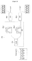
- FIG. 2 is a diagram illustrating an example of a modulator that is shown in FIG. 1 .
- FIG. 2 illustrates only one modulator 140a of two modulators 140a and 140b, and the modulator 140b can be formed equally to the modulator 140a.
- the modulator 140a includes Mach-Zehnder modulators 142a_1 and 142a_2 and a phase converter 144a.
- the Mach-Zehnder modulator 142a_1 receives an optical carrier and an I signal, and maps and outputs bit information of the I signal to a phase 0 or 180° of the optical carrier according to bit information of the input I signal.
- the Mach-Zehnder modulator 142a_2 receives an optical carrier and a Q signal, and maps bit information of the input Q signal to a phase 0 or 180° of the optical carrier according to bit information of the input Q signal to output the bit information to the phase converter 144a.
- the phase converter 144a converts a phase of the optical carrier to which the bit information of the Q signal is mapped by 90°. Thereby, the bit information of the Q signal is mapped to a phase 90° or 270° of the optical carrier.
- an I or Q signal is mapped to a corresponding phase of phases 0, 90°, 180°, and 270° of the optical carrier.
- the signal coupler 150 combines optical signals that are optically modulated by the modulators 140a and 140b to transmit the optical signals to the optical receiving apparatus 200.
- the signal coupler 150 can be formed by an optical filter, an optical coupler or a polarization controller, and an optical coupler.
- the optical receiving apparatus 200 includes a signal divider 210, interferometers 220a and 220b, balanced photo-detectors (BPD) 230a_1, 230a_2, 220b_1, and 220b_2, amplifiers 240a_1, 240a_2, 240b_1, and 240b_2, and a parallelizing device 250.
- BPD balanced photo-detectors
- the signal divider 210 receives an optical signal from the optical transmitting apparatus 100, separates the received optical signal into two optical signals having two wavelengths A - ⁇ ⁇ and ⁇ + ⁇ ⁇ , and outputs the separated optical signal to the interferometers 220a and 220b.
- the interferometers 220a and 220b convert the phase modulated optical signal to intensity modulated optical signal. In this way, demodulation technology using the interferometer delays one side path of the interferometer by a symbol period, and thus allows front and back bits to cause interference, thereby outputting a signal of 1 or 0 according to a phase difference of the front and back bits.
- the interferometers 220a and 220b according to an exemplary embodiment of the present invention use the Mach-Zehnder delay interferometer.
- FIG. 3 is a diagram illustrating an example of an interferometer that is shown in FIG. 1 .
- FIG. 3 illustrates only the interferometer 220a of the interferometers 220a and 220b that are allocated on an optical carrier basis, and two interferometers 220a and 220b can be formed with the same method.
- the interferometer 220a includes a coupler 222a and Mach-Zehnder delay interferometers (MZDI) 224a_1 and 224a_2.
- MZDI Mach-Zehnder delay interferometers
- the coupler 222a divides the input optical signal into two signals to output the two signals to the MZDIs 224a_1 and 224a_2.
- the MZDI 224a_1 has two output terminals, divides a signal that is input from the coupler 222a into two components, delays one side path by a symbol period T of a signal, and couples the two components. Therefore, constructive and destructive interference occurs at two output terminals of the MZDI 224a_1, respectively.
- the MZDI 224a_2 has two output terminals, divides another signal that is input from the coupler 222a into two signal components, delays one side path by a symbol period T of a signal, and couples the two signal components. Therefore, constructive and destructive interference occurs at two output terminals, respectively of the MZDI 224a_2.
- a phase difference between signals is adjusted to be +45° and -45° together with time delay.
- an I signal component and a Q signal component that are transmitted from the optical transmitting apparatus 100 can be restored, and in the MZDI 224a_1 and 224a_2, a signal in which a phase is modulated is converted to a signal in which a intensity is modulated.
- the BPDs 230a_1, 230a_2, 230b_1, and 230b_2 output two pairs of I and Q signals in which two pairs of an I signal component and a Q signal component that are demodulated with intensity modulation by the interferometers 220a and 220b are converted to an electric signal to the amplifiers 240a_1, 240a_2, 240b_1, and 240b_2, respectively.
- the amplifiers 240a_1, 240a_2, 240b_1, and 240b_2 amplify output signals of corresponding BPDs 230a_1, 230a_2, 230b_1, and 230b_2 to output the output signals to the parallelizing device 250.
- the parallelizing device 250 separates two pairs of I and Q signals that are output from the amplifiers 24a_1, 240a_2, and 240b_1, 240b_2 into the n-quantity of output signals.
- the control circuit 300 controls bias of using optoelectronic devices and monitors a state of the optical transceiver. Further, the control circuit 300 controls a phase of the modulators 140a and 140b and the interferometers 220a and 220b.
- FIG. 4 is a flowchart illustrating a method of transmitting light using an optical transmitting apparatus according to an exemplary embodiment of the present invention.
- FIG. 5 is a diagram illustrating the output of a dual carrier generator
- FIG. 6 is a diagram illustrating an optical carrier that is separated by a carrier separator.
- FIG. 7 is a diagram illustrating the output of two modulators
- FIG. 8 is a diagram illustrating the output of a signal coupler.
- the dual carrier generator 120 generates two optical carriers having wavelengths ⁇ - ⁇ A and A + ⁇ A that are separated by a predetermined wavelength 5 ⁇ from a central wavelength ⁇ (S410), as shown in FIG. 5 .
- two optical carriers may be generated while separated by the same gap from the central wavelength ⁇ and may be generated while separated by different gaps.
- the carrier separator 130 separates two optical carriers having wavelengths ⁇ - ⁇ ⁇ and ⁇ + ⁇ ⁇ and outputs the two optical carriers to the modulators 140a and 140b (S420), as shown in FIG. 6 .
- the serializing device 110 multiplexes the input n-quantity of electric signals into two pairs of I and Q signals I t1 /Q t1 and I t2 /Q t2 , outputs a pair of I and Q signals I t1 /Q t1 to the modulator 140a, and outputs another pair of I and Q signals I t2 /Q t2 to the modulator 140b (S430).
- the modulators 140a and 140b optically modulate the input I and Q signals I t1 /Q t1 and I t2 /Q t2 with a DQPSK method, and outputs the input I and Q signals to the signal coupler 150 (S440).
- a signal that is optically modulated with a DQPSK method by the modulators 140a and 140b can be represented, as shown in FIG. 7 .
- the signal coupler 150 combines optically modulated signals from the modulators 140a and 140b to transmit the signals to the optical receiving apparatus 200 (S450).
- a coupled signal of signals that are optically modulated with a DQPSK method by the modulators 140a and 140b can be represented, as shown in FIG. 8 .
- an optical signal that is optically modulated in the optical transmitting apparatus 100 is demodulated into an original signal via a signal divider 210, interferometers 220a and 220b, balanced photo-detectors (BPD) 230a_1, 230a_2, 220b_1, and 220b_2, amplifiers 240a_1, 240a_2, 240b_1, and 240b_2, and a parallelizing device 250 of the optical receiving apparatus 200.
- BPD balanced photo-detectors
- FIG. 9 is a flowchart illustrating a method of receiving light according to an exemplary embodiment of the present invention
- FIG. 10 is a diagram illustrating the output of a signal separator.
- the signal divider 210 separates an optical signal that is received from the optical transmitting apparatus 100 into an optical signal having wavelengths ⁇ - ⁇ ⁇ and ⁇ + ⁇ A , outputs an optical signal having the wavelength ⁇ - ⁇ to the interferometer 220a, and outputs an optical signal having the wavelength A + ⁇ ⁇ to the interferometer 220b (S910), as shown in FIG. 10 .
- the interferometers 220a and 220b each demodulate the input optical signals with intensity modulation to output the optical signals to the BPDs 230a_1, 230a_2, 220b_1, and 220b_2 (S920).
- the BPDs 230a_1, 230a_2, 230b_1, and 230b_2 convert a signal that is demodulated with intensity modulation to an electric signal (S930).
- a pair of I and Q signals I t1 /Q t1 are restored by the BPDs 230a_1 and 230a_2, and another pair of I and Q signals I t2 /Q t2 are restored by the BPDs 230b_1 and 230b_2.
- the amplifiers 240a_1, 240a_2, 240b_1, and 240b_2 amplify signals I t1 /Q t1 and I t2 /Q t2 that are output from the BPDs 230a_1, 230a_2, 220b_1, and 220b_2 to output the signals I t1 /Q t1 and I t2 /Q t2 to the parallelizing device 250 (S940).
- the parallelizing device 250 separates two pairs of I and Q signals I t1 /Q t1 and I t2 /Q t2 that are output from the amplifiers 240a_1, 240a_2, 240b_1, and 240b_2 into the n-quantity of output signals (S950).
- FIG. 11 is a diagram illustrating an example of a dual carrier generator that is shown in FIG. 1 .
- the dual carrier generator 120 includes a laser 122, a clock driver 124, and a Mach-Zehnder modulator 126.
- the laser 122 outputs a signal having a central wavelength ⁇ to output the signal to the Mach-Zehnder modulator 126.
- the clock driver 124 outputs an electrical clock signal having a pulse period of a wavelength ⁇ to the Mach-Zehnder modulator 126.
- the Mach-Zehnder modulator 126 receives a signal having a central wavelength ⁇ and an electrical clock signal having a gap of a wavelength ⁇ ⁇ and generates two electric signals, i.e., two optical carriers having wavelengths ⁇ - ⁇ ⁇ and ⁇ + ⁇ ⁇ that are separated by a wavelength ⁇ ⁇ from a central wavelength ⁇ .
- FIG. 12 is a diagram illustrating another example of a dual carrier generator that is shown in FIG. 1 .
- a dual carrier generator 120' includes a double laser source 122'.
- the double laser source 122' includes two lasers 122a and 122b, and each of the lasers 122a and 122b outputs a signal having wavelengths ⁇ - ⁇ ⁇ and ⁇ + ⁇ ⁇ . Because the dual carrier generator 120' generates a signal having wavelengths ⁇ - ⁇ ⁇ and ⁇ + ⁇ ⁇ from each of the lasers 122a and 122b, it is unnecessary to separate a signal in the carrier separator 130. Therefore, the lasers 122a and 122b directly output a signal having wavelengths ⁇ - ⁇ ⁇ and ⁇ + ⁇ ⁇ to the modulators 140a and 140b.
- FIG. 13 is a diagram illustrating an example of a signal coupler that is shown in FIG. 1 .
- the signal coupler 150 includes a polarization controller 152 and a polarization combiner 154.
- the polarization controller 152 adjusts polarization of one of optically modulated optical signals from the modulators 140a and 140b, and outputs the optical signal to the polarization combiner 154.
- the polarization controller 152 can adjust polarization of one of optically modulated optical signals from the modulators 140a and 140b such that polarization of two optically modulated optical signals from the modulators 140a and 140b is orthogonal.
- the polarization combiner 154 couples another one of optical signals that are optically modulated from the modulators 140a and 140b and an optical signal in which polarization is adjusted from the polarization controller 152.
- the polarization combiner 154 couples the optical signals.
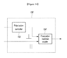
- FIG. 14 is a diagram illustrating another example of a signal coupler that is shown in FIG. 1 .
- a signal coupler 150' includes a polarization controller 152 and a polarization maintaining coupler 154'. That is, while sustaining polarization using the polarization maintaining coupler 154' instead of the polarization combiner 154 that is shown in FIG. 13 , another one of optically modulated optical signals from the modulators 140a and 140b and an optical signal in which polarization is adjusted from the polarization controller 152 can be coupled. According to another exemplary embodiment of the present invention, two optical carriers may be directly connected to the outside of an optical transceiver without using the signal coupler 150 and the signal separator 210.
- the optical transceiver according to an exemplary embodiment of the present invention can transmit a signal with a high transmission speed and a low symbol rate speed without using an ADC or a DSP.
- An exemplary embodiment of the present invention may not only be embodied through the above-described apparatus and method, but may also be embodied through a program that realizes a function corresponding to a configuration of the exemplary embodiment of the present invention or a recording medium on which the program is recorded, and can be easily embodied by a person of ordinary skill in the art from the description of the foregoing exemplary embodiment.
Landscapes
- Physics & Mathematics (AREA)
- Electromagnetism (AREA)
- Engineering & Computer Science (AREA)
- Computer Networks & Wireless Communication (AREA)
- Signal Processing (AREA)
- Optics & Photonics (AREA)
- Optical Communication System (AREA)
Abstract
Description
- The present invention relates to an apparatus and method for transmitting light, and an apparatus and method for receiving light.
- Internet traffic has gradually increased due to the advent of an Ethernet-based service such as Internet TV and user created contents (UCC), such that it is essentially requested to enlarge an area of a network.
- At a data traffic focusing point such as a high performance computer, server, data center, enterprise network, and Internet exchange center, in order to satisfy a bandwidth request, a signal of 40G or more per wavelength is generated. In order to transmit such a high speed signal, an optical transmitter uses a phase shift keying (PSK) method that modulates a phase of an optical signal or a quadrature phase shift keying (QPSK) method that can transmit 2 bits or more per symbol.
- In general, because a PSK or QPSK signal is transmitted using a single carrier, polarization mode dispersion and chromatic dispersion generating in an optical line should be compensated on a channel basis in a reception terminal. For example, when the QPSK method is used, if the bit rate is B, the symbol rate is the bit rate that is divided into the number of bits that can be transmitted with each symbol and thus the symbol rate becomes B/2. Therefore, a bandwidth of optoelectronic device to be 1/2 of a bit rate is required.
- In order to solve such a problem, a dual polarization-quadrature phase shift keying (DP-QPSK) of simultaneously using the QPSK and polarization characteristics of an optical signal is suggested. Because the DP-QPSK can lower the symbol rate to B/4, the bandwidth of optoelectronic devices can be reduced and pulse dispersion of an optical signal generating in an optical line can be suppressed. However, in order to separate two polarizations and restore a signal, the phase of the optical signal should be detected and thus an analog to digital converter (ADC) and a digital signal processor (DSP) operating at a high speed in a reception terminal are always necessary.
- A DP-DQPSK method of lowering the symbol transmission rate to B/4 using polarization characteristics of an optical signal while not using the ADC and the DSP is suggested. The DP-DQPSK method converts a phase modulated optical signal to intensity modulation optical signal and receives the optical signal using a delay interferometer in a reception terminal, and thus does not require the ADC and the DSP. However, the reception terminal requires a complicated polarization controller for separating polarization.
- The present invention has been made in an effort to provide an apparatus and method for transmitting light and an apparatus and method for receiving light having advantages of transmitting a signal at a high transmission speed and a low symbol rate speed without using an ADC, a DSP, and a polarization controller.
- An exemplary embodiment of the present invention provides an optical transmitting apparatus including a dual carrier generator, a serializing device, a first modulator, a second modulator, and a signal coupler. The dual carrier generator generates first and second optical carriers. The serializing device multiplexes a plurality of input signals into two pairs of I and Q signals. The first modulator modulates a pair of I and Q signals using a phase of the first optical carrier. The second modulator modulates another pair of I and Q signals using a phase of the second optical carrier. The signal coupler couples and transmits signals that are modulated by the first and second modulators.
- Another embodiment of the present invention provides an optical receiving apparatus including a first interferometer, a second interferometer, first and second balanced photo-detectors, and a parallelizing device. The first interferometer restores an input optical signal into a pair of I and Q signal components by demodulating with intensity modulation. The second interferometer restores an input optical signal into another pair of I and Q signal components by demodulating with intensity modulation. The first and second balanced photo-detectors output a pair of I and Q signals by converting a pair of I and Q signal components to an electric signal. The third and fourth balanced photo-detectors output another pair of I and Q signals by converting another pair of I and Q signal components to an electric signal. The parallelizing device separates the two pairs of I and Q signals into a plurality of signals by demultiplexing.
- Yet another embodiment of the present invention provides a method of transmitting an optical signal in an optical transmitting apparatus. The method includes generating first and second optical carriers, multiplexing a plurality of input signals into two pairs of I and Q signals, optically modulating two pairs of I and Q signals using a phase of the first and second optical carriers, and transmitting the two modulated optical signals.
- Yet another embodiment of the present invention provides a method of receiving an optical signal in an optical receiving apparatus. The method includes converting two optical signals to two pairs of I and Q signals by modulating the input two optical signals with intensity modulation using a phase difference of two optical signals having different wavelengths, and separating the two pairs of I and Q signals into a plurality of signals.
- According to an exemplary embodiment of the present invention, because an analog to digital converter (ADC), a high speed digital signal processor (DSP), and a complicated polarization controller are not used, the structure of an optical transceiver becomes simple.
- Further, an optical signal can be transmitted with a high transmission speed and a low symbol rate speed through an optical transceiver of a simple structure. Therefore, pulse dispersion generated in an optical line can be prevented while being capable of performing high speed transmission that is required in an optical communication network.
-
-
FIG. 1 is a diagram illustrating an optical transceiver according to an exemplary embodiment of the present invention. -
FIG. 2 is a diagram illustrating an example of a modulator that is shown inFIG. 1 . -
FIG. 3 is a diagram illustrating an example of an interferometer that is shown inFIG. 1 . -
FIG. 4 is a flowchart illustrating a method of transmitting light using an optical transmitting apparatus according to an exemplary embodiment of the present invention. -
FIG. 5 is a diagram illustrating the output of a dual carrier generator. -
FIG. 6 is a diagram illustrating an optical carrier that is separated by a carrier separator. -
FIG. 7 is a diagram illustrating the output of two modulators. -
FIG. 8 is a diagram illustrating the output of a signal coupler. -
FIG. 9 is a flowchart illustrating a method of receiving light according to an exemplary embodiment of the present invention. -
FIG. 10 is a diagram illustrating the output of a signal separator. -
FIG. 11 is a diagram illustrating an example of a dual carrier generator that is shown inFIG. 1 . -
FIG. 12 is a diagram illustrating another example of a dual carrier generator that is shown inFIG. 1 . -
FIG. 13 is a diagram illustrating an example of a signal coupler that is shown inFIG. 1 . -
FIG. 14 is a diagram illustrating another example of a signal coupler that is shown inFIG. 1 . - In the following detailed description, only certain exemplary embodiments of the present invention have been shown and described, simply by way of illustration. As those skilled in the art would realize, the described embodiments may be modified in various different ways, all without departing from the spirit or scope of the present invention. Accordingly, the drawings and description are to be regarded as illustrative in nature and not restrictive. Like reference numerals designate like elements throughout the specification.
- In addition, in the entire specification and claims, unless explicitly described to the contrary, the word "comprise" and variations such as "comprises" or "comprising" will be understood to imply the inclusion of stated elements but not the exclusion of any other elements.
- Now, an apparatus and method for transmitting light and an apparatus and method for receiving light according to an exemplary embodiment of the present invention will be described in detail with reference to the drawings.
-
FIG. 1 is a diagram illustrating an optical transceiver according to an exemplary embodiment of the present invention. - Referring to
FIG. 1 , the optical transceiver includes anoptical transmitting apparatus 100, anoptical receiving apparatus 200, and acontrol circuit 300. - The
optical transmitting apparatus 100 includes a serializingdevice 110, adual carrier generator 120, acarrier separator 130,modulators signal coupler 150. - The serializing
device 110 multiplexes the input n-quantity of electric signals into four electric signals It1, Qt1, It2, and Qt2 to output the electric signals to themodulators modulator 140a, and the remaining pair of I and Q signals It2/Qt2 are input to anothermodulator 140b. - The
dual carrier generator 120 generates two optical carriers. - The
carrier separator 130 separates two optical carriers, outputs one optical carrier to themodulator 140a, and outputs the remaining optical carrier to themodulator 140b. - The
modulators - The
modulators -
FIG. 2 is a diagram illustrating an example of a modulator that is shown inFIG. 1 .FIG. 2 illustrates only onemodulator 140a of twomodulators modulator 140b can be formed equally to themodulator 140a. - Referring to
FIG. 2 , themodulator 140a includes Mach-Zehnder modulators 142a_1 and 142a_2 and aphase converter 144a. - The Mach-Zehnder modulator 142a_1 receives an optical carrier and an I signal, and maps and outputs bit information of the I signal to a phase 0 or 180° of the optical carrier according to bit information of the input I signal.
- The Mach-Zehnder modulator 142a_2 receives an optical carrier and a Q signal, and maps bit information of the input Q signal to a phase 0 or 180° of the optical carrier according to bit information of the input Q signal to output the bit information to the
phase converter 144a. - The
phase converter 144a converts a phase of the optical carrier to which the bit information of the Q signal is mapped by 90°. Thereby, the bit information of the Q signal is mapped to a phase 90° or 270° of the optical carrier. - Therefore, an I or Q signal is mapped to a corresponding phase of phases 0, 90°, 180°, and 270° of the optical carrier.
- Referring again to
FIG. 1 , thesignal coupler 150 combines optical signals that are optically modulated by themodulators optical receiving apparatus 200. Thesignal coupler 150 can be formed by an optical filter, an optical coupler or a polarization controller, and an optical coupler. - The
optical receiving apparatus 200 includes asignal divider 210,interferometers parallelizing device 250. - The
signal divider 210 receives an optical signal from theoptical transmitting apparatus 100, separates the received optical signal into two optical signals having two wavelengths A -δ λ and λ +δ λ , and outputs the separated optical signal to theinterferometers - The
interferometers - The
interferometers -
FIG. 3 is a diagram illustrating an example of an interferometer that is shown inFIG. 1 .FIG. 3 illustrates only theinterferometer 220a of theinterferometers interferometers - Referring to
FIG. 3 , theinterferometer 220a includes acoupler 222a and Mach-Zehnder delay interferometers (MZDI) 224a_1 and 224a_2. - The
coupler 222a divides the input optical signal into two signals to output the two signals to the MZDIs 224a_1 and 224a_2. - The MZDI 224a_1 has two output terminals, divides a signal that is input from the
coupler 222a into two components, delays one side path by a symbol period T of a signal, and couples the two components. Therefore, constructive and destructive interference occurs at two output terminals of the MZDI 224a_1, respectively. - Similarly, the MZDI 224a_2 has two output terminals, divides another signal that is input from the
coupler 222a into two signal components, delays one side path by a symbol period T of a signal, and couples the two signal components. Therefore, constructive and destructive interference occurs at two output terminals, respectively of the MZDI 224a_2. In this case, in two MZDIs 224a_1 and 224a_2, a phase difference between signals is adjusted to be +45° and -45° together with time delay. Thereby, an I signal component and a Q signal component that are transmitted from theoptical transmitting apparatus 100 can be restored, and in the MZDI 224a_1 and 224a_2, a signal in which a phase is modulated is converted to a signal in which a intensity is modulated. - Referring again to
FIG. 1 , the BPDs 230a_1, 230a_2, 230b_1, and 230b_2 output two pairs of I and Q signals in which two pairs of an I signal component and a Q signal component that are demodulated with intensity modulation by theinterferometers - The amplifiers 240a_1, 240a_2, 240b_1, and 240b_2 amplify output signals of corresponding BPDs 230a_1, 230a_2, 230b_1, and 230b_2 to output the output signals to the
parallelizing device 250. - The parallelizing
device 250 separates two pairs of I and Q signals that are output from the amplifiers 24a_1, 240a_2, and 240b_1, 240b_2 into the n-quantity of output signals. - The
control circuit 300 controls bias of using optoelectronic devices and monitors a state of the optical transceiver. Further, thecontrol circuit 300 controls a phase of the modulators 140a and 140b and theinterferometers -
FIG. 4 is a flowchart illustrating a method of transmitting light using an optical transmitting apparatus according to an exemplary embodiment of the present invention.FIG. 5 is a diagram illustrating the output of a dual carrier generator, andFIG. 6 is a diagram illustrating an optical carrier that is separated by a carrier separator. Further,FIG. 7 is a diagram illustrating the output of two modulators, andFIG. 8 is a diagram illustrating the output of a signal coupler. - Referring to
FIG. 4 , thedual carrier generator 120 generates two optical carriers having wavelengths λ -δ A and A +δ A that are separated by a predetermined wavelength 5 λ from a central wavelength λ (S410), as shown inFIG. 5 . In this case, two optical carriers may be generated while separated by the same gap from the central wavelength λ and may be generated while separated by different gaps. - The
carrier separator 130 separates two optical carriers having wavelengths λ -δ λ and λ +δ λ and outputs the two optical carriers to themodulators FIG. 6 . - Further, the serializing
device 110 multiplexes the input n-quantity of electric signals into two pairs of I and Q signals It1/Qt1 and It2/Qt2, outputs a pair of I and Q signals It1/Qt1 to themodulator 140a, and outputs another pair of I and Q signals It2/Qt2 to themodulator 140b (S430). - The
modulators modulators FIG. 7 . - Thereafter, the
signal coupler 150 combines optically modulated signals from themodulators modulators FIG. 8 . - In this way, an optical signal that is optically modulated in the
optical transmitting apparatus 100 is demodulated into an original signal via asignal divider 210,interferometers parallelizing device 250 of theoptical receiving apparatus 200. -
FIG. 9 is a flowchart illustrating a method of receiving light according to an exemplary embodiment of the present invention, andFIG. 10 is a diagram illustrating the output of a signal separator. - Referring to
FIG. 9 , thesignal divider 210 separates an optical signal that is received from theoptical transmitting apparatus 100 into an optical signal having wavelengths λ -δ λ and λ +δ A , outputs an optical signal having the wavelength λ - δλ to theinterferometer 220a, and outputs an optical signal having the wavelength A +δ λ to theinterferometer 220b (S910), as shown inFIG. 10 . - The
interferometers - The BPDs 230a_1, 230a_2, 230b_1, and 230b_2 convert a signal that is demodulated with intensity modulation to an electric signal (S930). In this case, a pair of I and Q signals It1/Qt1 are restored by the BPDs 230a_1 and 230a_2, and another pair of I and Q signals It2/Qt2 are restored by the BPDs 230b_1 and 230b_2.
- The amplifiers 240a_1, 240a_2, 240b_1, and 240b_2 amplify signals It1/Qt1 and It2/Qt2 that are output from the BPDs 230a_1, 230a_2, 220b_1, and 220b_2 to output the signals It1/Qt1 and It2/Qt2 to the parallelizing device 250 (S940).
- The parallelizing
device 250 separates two pairs of I and Q signals It1/Qt1 and It2/Qt2 that are output from the amplifiers 240a_1, 240a_2, 240b_1, and 240b_2 into the n-quantity of output signals (S950). -
FIG. 11 is a diagram illustrating an example of a dual carrier generator that is shown inFIG. 1 . - Referring to
FIG. 11 , thedual carrier generator 120 includes alaser 122, aclock driver 124, and a Mach-Zehnder modulator 126. - The
laser 122 outputs a signal having a central wavelength λ to output the signal to the Mach-Zehnder modulator 126. - The
clock driver 124 outputs an electrical clock signal having a pulse period of a wavelength δλ to the Mach-Zehnder modulator 126. - The Mach-
Zehnder modulator 126 receives a signal having a central wavelength λ and an electrical clock signal having a gap of a wavelength δ λ and generates two electric signals, i.e., two optical carriers having wavelengths λ -δ λ and λ +δ λ that are separated by a wavelength δ λ from a central wavelength λ . -
FIG. 12 is a diagram illustrating another example of a dual carrier generator that is shown inFIG. 1 . - Referring to
FIG. 12 , a dual carrier generator 120' includes a double laser source 122'. The double laser source 122' includes twolasers lasers lasers carrier separator 130. Therefore, thelasers modulators - When output signals of the two
lasers carrier separator 130 and output to themodulators -
FIG. 13 is a diagram illustrating an example of a signal coupler that is shown inFIG. 1 . - Referring to
FIG. 13 , thesignal coupler 150 includes apolarization controller 152 and apolarization combiner 154. - The
polarization controller 152 adjusts polarization of one of optically modulated optical signals from themodulators polarization combiner 154. In this case, thepolarization controller 152 can adjust polarization of one of optically modulated optical signals from themodulators modulators - The
polarization combiner 154 couples another one of optical signals that are optically modulated from themodulators polarization controller 152. When polarization of an optical signal is input to a predetermined polarizing axis, thepolarization combiner 154 couples the optical signals. -
FIG. 14 is a diagram illustrating another example of a signal coupler that is shown inFIG. 1 . - Referring to
FIG. 14 , a signal coupler 150' includes apolarization controller 152 and a polarization maintaining coupler 154'. That is, while sustaining polarization using the polarization maintaining coupler 154' instead of thepolarization combiner 154 that is shown inFIG. 13 , another one of optically modulated optical signals from themodulators polarization controller 152 can be coupled. According to another exemplary embodiment of the present invention, two optical carriers may be directly connected to the outside of an optical transceiver without using thesignal coupler 150 and thesignal separator 210. - Therefore, the optical transceiver according to an exemplary embodiment of the present invention can transmit a signal with a high transmission speed and a low symbol rate speed without using an ADC or a DSP.
- An exemplary embodiment of the present invention may not only be embodied through the above-described apparatus and method, but may also be embodied through a program that realizes a function corresponding to a configuration of the exemplary embodiment of the present invention or a recording medium on which the program is recorded, and can be easily embodied by a person of ordinary skill in the art from the description of the foregoing exemplary embodiment.
- While this invention has been described in connection with what is presently considered to be practical exemplary embodiments, it is to be understood that the invention is not limited to the disclosed embodiments, but, on the contrary, is intended to cover various modifications and equivalent arrangements included within the spirit and scope of the appended claims.
Claims (20)
- An optical transmitting apparatus, comprising:a dual carrier generator that generates first and second optical carriers;a serializing device that multiplexes a plurality of input signals into two pairs of in-phase (I) and quadrature-phase (Q) signals;a first modulator that modulates and outputs a pair of I and Q signals using a phase of the first optical carrier; anda second modulator that modulates and outputs another pair of I and Q signals using a phase of the second optical carrier.
- The optical transmitting apparatus of claim 1, wherein the first and second modulators use a differential quadrature phase shift keying (DQPSK) modulation method.
- The optical transmitting apparatus of claim 1, wherein the dual carrier generator comprises:a laser that generates a signal of a central wavelength;a clock driver that generates an electrical clock signal; anda Mach-Zehnder modulator that generates the first and second optical carriers by separating by a pulse period of the clock signal from the central wavelength.
- The optical transmitting apparatus of claim 3, further comprising a carrier separator that separates the first and second optical carriers to output the first and second optical carriers to the first and second modulators.
- The optical transmitting apparatus of claim 1, wherein the dual carrier generator comprises first and second lasers that generate the first and second optical carriers having each wavelength.
- The optical transmitting apparatus of claim 1, further comprising a signal coupler that couple signals that are modulated by the first and second modulators to transmit the coupled signal to an optical receiving apparatus.
- The optical transmitting apparatus of claim 6, wherein the signal coupler comprises:a polarization controller that adjusts polarization of one of signals that are optically modulated by the first and second modulators; anda polarization combiner that combines a signal in which polarizing is adjusted and another signal of signals that are modulated by the first and second modulators.
- The optical transmitting apparatus of claim 6, wherein the signal coupler comprises:a polarization controller that adjusts polarization of one of signals that are optically modulated by the first and second modulators; anda polarization maintaining coupler that couples a signal in which polarizing is adjusted and another signal of signals that are modulated by the first and second modulators.
- An optical receiving apparatus, comprising:a first interferometer that restores an input optical signal into a pair of I and Q signal components by demodulating with intensity modulation;a second interferometer that restores an input optical signal into another pair of I and Q signal components by demodulating with intensity modulation;first and second balanced photo-detectors that output a pair of I and Q signals by converting the pair of I and Q signal components to an electric signal;third and fourth balanced photo-detectors that output another pair of I and Q signals by converting another pair of I and Q signal components to an electric signal; anda parallelizing device that separates the two pairs of I and Q signals into a plurality of signals by demultiplexing.
- The optical receiving apparatus of claim 9, wherein the first and second interferometers each comprise:a coupler that separates the input optical signal into two signals;a first Mach-Zehnder delay interferometer that divides one of two signals into two signal components and that delays a signal component of one side path and couples the delayed signal component and another signal component of two signal components to output the I signal component; anda second Mach-Zehnder delay interferometer that divides another one of two signals into two signal components and that delays a signal component of one side path and couples the delayed signal component and another signal component of two signal components to output the Q signal component,wherein the first and second interferometers each generate the input optical signal at ±45°.
- The optical receiving apparatus of claim 10, wherein the first and second Mach-Zehnder delay interferometers delay the signal component of one side path by a symbol period.
- The optical receiving apparatus of claim 9, further comprising first to fourth amplifiers that amplify signals that are output from the first to fourth balanced photo-detectors, respectively.
- The optical receiving apparatus of claim 9, further comprising a signal divider that separates the input optical signal into two optical signals having different wavelengths to output the optical signals to the first and second interferometers.
- A method of transmitting an optical signal in an optical transmitting apparatus, the method comprising:generating first and second optical carriers;multiplexing a plurality of input signals into two pairs of I and Q signals;optically modulating the two pairs of I and Q signals using a phase of the first and second optical carriers; andtransmitting the two modulated optical signals.
- The method of claim 14, wherein the optically modulating of two pairs of I and Q signals comprises modulating the two pairs of I and Q signals with the differential quadrature phase shift keying (DQPSK) method.
- The method of claim 14, wherein the generating of first and second optical carriers comprises:generating a signal having a central wavelength;generating an electrical clock signal; andgenerating the first and second optical carriers by separating by a pulse period of the clock signal from the central wavelength.
- The method of claim 14, wherein the transmitting of the modulated two optical signals comprises coupling the two optical signals.
- A method of receiving an optical signal in an optical receiving apparatus, the method comprising:converting the optical signal to I and Q signals using a phase difference of two optical signals having different wavelengths; andseparating two pairs of I and Q signals into a plurality of signals.
- The method of claim 18, wherein the converting of the optical signal to I and Q signals comprises:delaying a phase of one of the two optical signals;dividing one optical signal having a delayed phase into two first signal components;delaying a signal of one side path of the two first signal components and coupling two signal components;delaying a phase of another one of the two optical signals;dividing another one optical signal having a delayed phase into two second signal components; anddelaying a signal of one side path of the two second signal components and coupling two signal components.
- The method of claim 19, wherein the delaying of a phase of one of the two optical signals and the delaying of a phase of another one of the two optical signals comprise delaying a phase by +45° and -45°.
Applications Claiming Priority (3)
| Application Number | Priority Date | Filing Date | Title |
|---|---|---|---|
| KR20090067998 | 2009-07-24 | ||
| KR1020100065956A KR101382619B1 (en) | 2009-07-24 | 2010-07-08 | Apparatus and method for optical transmitting, and apparatus and method for optical receiving |
| PCT/KR2010/004582 WO2011010827A2 (en) | 2009-07-24 | 2010-07-14 | Optical transmitting apparatus and method, and optical receiving device and method |
Publications (1)
| Publication Number | Publication Date |
|---|---|
| EP2458749A2 true EP2458749A2 (en) | 2012-05-30 |
Family
ID=43771084
Family Applications (1)
| Application Number | Title | Priority Date | Filing Date |
|---|---|---|---|
| EP10802420A Withdrawn EP2458749A2 (en) | 2009-07-24 | 2010-07-14 | Optical transmitting apparatus and method, and optical receiving device and method |
Country Status (5)
| Country | Link |
|---|---|
| US (1) | US20120121264A1 (en) |
| EP (1) | EP2458749A2 (en) |
| KR (1) | KR101382619B1 (en) |
| CN (1) | CN102549948A (en) |
| WO (1) | WO2011010827A2 (en) |
Families Citing this family (11)
| Publication number | Priority date | Publication date | Assignee | Title |
|---|---|---|---|---|
| CN105099570B (en) * | 2014-05-22 | 2018-08-17 | 复旦大学 | Orthogonal multiple carrier light source and PDM-QPSK sender units |
| US9325419B1 (en) * | 2014-11-07 | 2016-04-26 | Inphi Corporation | Wavelength control of two-channel DEMUX/MUX in silicon photonics |
| GB2538793A (en) | 2015-05-29 | 2016-11-30 | Oclaro Tech Ltd | Multiple carrier |
| WO2017165427A1 (en) * | 2016-03-21 | 2017-09-28 | Kaiam Corp. | Optical interconnect having optical splitters and modulators integrated on same chip |
| CN109075866A (en) * | 2016-07-11 | 2018-12-21 | 华为技术有限公司 | Optical signal transmitter, receiver, transmission method and system |
| KR102220895B1 (en) | 2016-11-16 | 2021-03-02 | 한국전자통신연구원 | Optical transmitter |
| US10715256B1 (en) * | 2019-02-18 | 2020-07-14 | Nokia Solutions And Networks Oy | Recovery of phase-modulated data from an optical signal via intensity measurements |
| KR102280189B1 (en) * | 2019-10-31 | 2021-07-23 | 한국원자력연구원 | Lidar apparatus |
| KR102415791B1 (en) | 2021-02-08 | 2022-06-30 | 연세대학교 산학협력단 | Optical Transmission Apparatus and Method for Pre-Compensating Phase Signal Distortion |
| KR102515056B1 (en) | 2021-10-28 | 2023-03-27 | 연세대학교 산학협력단 | Optical Transmission Apparatus And Method Capable Of Mitigating Inter-Dimensional Interference |
| CN115225247B (en) * | 2022-07-11 | 2023-12-01 | 北京邮电大学 | Phase modulation loop-back time synchronization device, method and system |
Family Cites Families (38)
| Publication number | Priority date | Publication date | Assignee | Title |
|---|---|---|---|---|
| US7146103B2 (en) * | 1999-12-29 | 2006-12-05 | Forster Energy Llc | Optical communications using multiplexed single sideband transmission and heterodyne detection |
| US6525857B1 (en) * | 2000-03-07 | 2003-02-25 | Opvista, Inc. | Method and apparatus for interleaved optical single sideband modulation |
| US7076169B2 (en) * | 2000-09-26 | 2006-07-11 | Celight, Inc. | System and method for orthogonal frequency division multiplexed optical communication |
| US7085499B2 (en) * | 2001-11-15 | 2006-08-01 | Hrl Laboratories, Llc | Agile RF-lightwave waveform synthesis and an optical multi-tone amplitude modulator |
| KR100584433B1 (en) * | 2003-11-25 | 2006-05-26 | 삼성전자주식회사 | Differential Polarization Modulation Optical Transmission System |
| US7577367B2 (en) * | 2004-06-15 | 2009-08-18 | Op Vista Incorporated | Optical communication using duobinary modulation |
| US8488967B2 (en) * | 2005-02-18 | 2013-07-16 | Telcordia Technologies, Inc. | System and method for OCDMA-based photonic layer security robustness to archival attack |
| JP4710387B2 (en) * | 2005-04-06 | 2011-06-29 | 富士通株式会社 | Optical receiver and optical receiving method corresponding to differential M phase shift keying |
| JP4516907B2 (en) * | 2005-08-26 | 2010-08-04 | 富士通株式会社 | Optical receiver and control method thereof |
| US7561807B2 (en) * | 2006-01-17 | 2009-07-14 | Alcatel-Lucent Usa Inc. | Use of beacons in a WDM communication system |
| JP4563944B2 (en) * | 2006-01-31 | 2010-10-20 | 富士通株式会社 | Optical transmitter |
| JP4806317B2 (en) * | 2006-08-30 | 2011-11-02 | 富士通株式会社 | Phase monitor device in optical receiver |
| US20080063396A1 (en) * | 2006-09-12 | 2008-03-13 | Nec Laboratories America, Inc. | Optical Subchannels From a Single Lightwave Source |
| EP2071747B1 (en) * | 2006-09-26 | 2015-02-18 | Hitachi, Ltd. | Optical electric field receiver and optical transmission system |
| JP5405716B2 (en) * | 2006-09-29 | 2014-02-05 | 富士通株式会社 | Optical transmitter |
| US7965947B2 (en) * | 2006-12-05 | 2011-06-21 | Nec Laboratories America, Inc. | Wavelength division multiplexing passive optical network architecture with source-free optical network units |
| GB2445588A (en) * | 2006-12-16 | 2008-07-16 | Qinetiq Ltd | Optical Correlation Apparatus with parallel optical signals |
| JP4522417B2 (en) * | 2007-01-15 | 2010-08-11 | 富士通株式会社 | Light modulation apparatus and light modulation method |
| JP2008187223A (en) * | 2007-01-26 | 2008-08-14 | Hitachi Communication Technologies Ltd | Control method of optical phase modulator |
| JP4906103B2 (en) * | 2007-07-06 | 2012-03-28 | 日本電信電話株式会社 | Optical modulation circuit and optical transmission system |
| US20090067843A1 (en) * | 2007-07-17 | 2009-03-12 | Way Winston I | Optical Wavelength-Division-Multiplexed (WDM) Comb Generator Using a Single Laser |
| JP4973362B2 (en) * | 2007-07-24 | 2012-07-11 | 富士通株式会社 | Optical receiver and control method thereof |
| JP4983466B2 (en) * | 2007-07-30 | 2012-07-25 | 富士通株式会社 | Optical modulation device, optical modulation method, and optical transmission device |
| US8463141B2 (en) * | 2007-09-14 | 2013-06-11 | Alcatel Lucent | Reconstruction and restoration of two polarization components of an optical signal field |
| JP5168685B2 (en) * | 2007-09-18 | 2013-03-21 | 独立行政法人情報通信研究機構 | Quadrature amplitude modulation signal generator |
| JP5012457B2 (en) * | 2007-11-30 | 2012-08-29 | 富士通株式会社 | DQPSK optical receiver |
| US8249463B2 (en) * | 2007-12-07 | 2012-08-21 | Infinera Corporation | Skew compensation across polarized optical channels |
| US8032036B2 (en) * | 2007-12-10 | 2011-10-04 | Verizon Patent And Licensing Inc. | DQPSK/DPSK optical receiver with tunable optical fibers |
| CN101459638B (en) * | 2007-12-14 | 2012-03-21 | 华为技术有限公司 | Receiving apparatus and method for differential quadrature phased shift keying DQPSK signal |
| WO2009105281A2 (en) * | 2008-02-22 | 2009-08-27 | Opvista Incorporated | Spectrally efficient parallel optical wdm channels for long-haul man and wan optical networks |
| JP2009200915A (en) * | 2008-02-22 | 2009-09-03 | Fujitsu Ltd | Optical dqpsk receiver, and optical phase monitoring apparatus to be used in the same |
| ATE476801T1 (en) * | 2008-04-11 | 2010-08-15 | Alcatel Lucent | MODULATION SCHEME WITH INCREASED NUMBER OF POLARIZATION STATES |
| JP5186993B2 (en) * | 2008-04-30 | 2013-04-24 | 富士通株式会社 | Polarization multiplexed optical transceiver |
| US8090271B2 (en) * | 2008-05-01 | 2012-01-03 | Nec Laboratories America, Inc. | Differential delay receiver using cross-polarization interferometer for PolMux-DPSK system |
| JP5476697B2 (en) * | 2008-09-26 | 2014-04-23 | 富士通株式会社 | Optical signal transmitter |
| CN101729149A (en) * | 2008-10-22 | 2010-06-09 | 华为技术有限公司 | Method, device and system for photolyzing, polarizing and multiplexing optical carrier |
| US8204377B2 (en) * | 2008-10-23 | 2012-06-19 | Alcatel Lucent | System, method and apparatus for joint self phase modulation compensation for coherent optical polarization-division-multiplexed orthogonal-frequency division-multiplexing systems |
| US8699882B2 (en) * | 2009-01-08 | 2014-04-15 | Ofidium Pty Ltd | Signal method and apparatus |
-
2010
- 2010-07-08 KR KR1020100065956A patent/KR101382619B1/en not_active Expired - Fee Related
- 2010-07-14 EP EP10802420A patent/EP2458749A2/en not_active Withdrawn
- 2010-07-14 WO PCT/KR2010/004582 patent/WO2011010827A2/en not_active Ceased
- 2010-07-14 CN CN2010800426907A patent/CN102549948A/en active Pending
- 2010-07-14 US US13/386,564 patent/US20120121264A1/en not_active Abandoned
Non-Patent Citations (1)
| Title |
|---|
| See references of WO2011010827A2 * |
Also Published As
| Publication number | Publication date |
|---|---|
| US20120121264A1 (en) | 2012-05-17 |
| WO2011010827A3 (en) | 2011-04-21 |
| KR101382619B1 (en) | 2014-04-07 |
| WO2011010827A2 (en) | 2011-01-27 |
| KR20110010558A (en) | 2011-02-01 |
| CN102549948A (en) | 2012-07-04 |
Similar Documents
| Publication | Publication Date | Title |
|---|---|---|
| US20120121264A1 (en) | Apparatus and method for transmitting light, and apparatus and method for receiving light | |
| EP2197165B1 (en) | Efficient QAM signal generation | |
| EP1760520B1 (en) | Differential quadrature phase-shift modulator and method for setting driving voltage thereof | |
| US20100189437A1 (en) | Optical receiver and optical reception method compatible with differential quadrature phase shift keying | |
| EP2421180B1 (en) | Method, device and system for generating and receiving phase polarization modulated signal | |
| US20100239264A1 (en) | Optical transmission system, apparatus and method | |
| US8837947B2 (en) | Apparatus for pseudo-return-to-zero modulation | |
| KR20110030136A (en) | Polarization splitters, optical hybrids and optical receivers comprising them | |
| US7555061B2 (en) | Optical communication device | |
| JP2011530885A (en) | Frequency offset polarization multiplexed modulation format and system incorporating the same | |
| EP1536578B1 (en) | Differential polarization shift-keying optical transmission system | |
| US20120195600A1 (en) | Reference-signal distribution in an optical transport system | |
| JP5321591B2 (en) | Optical transmitter, optical receiver, and optical communication system | |
| US20110222865A1 (en) | Method and apparatus for transmission of two modulated signals via an optical channel | |
| US8428471B2 (en) | Optical access system for dual service network | |
| CN101626274A (en) | Method for generating star hexadecimal optical signals, optical transmitter and system | |
| US8165477B2 (en) | Light receiving apparatus using DQPSK demodulation method, and DQPSK demodulation method | |
| US20120287949A1 (en) | Polarization multiplexed signaling using time shifting in return-to-zero format | |
| JP4730560B2 (en) | Optical transmission system, optical transmission method, and optical transmitter | |
| JP5218143B2 (en) | Optical transmitter, optical receiver, and optical communication system | |
| US20100150576A1 (en) | Optical transmitting apparatus for return-to-zero differential phase-shift-keying (rz-dpsk) or return-to-zero differential quadrature phase shift keying (rz-dqpsk) | |
| JPWO2010026757A1 (en) | Transmitting apparatus, receiving apparatus, optical transmission system, and optical transmission method | |
| JP2011182198A (en) | Optical phase noise suppression circuit, phase fluctuation detection circuit, and phase fluctuation detection method | |
| KR101282414B1 (en) | Optical transmitting apparatus for RZ-DPSK and RZ-DQPSK | |
| JP2010062654A (en) | Optical transmission apparatus and light transmission system |
Legal Events
| Date | Code | Title | Description |
|---|---|---|---|
| PUAI | Public reference made under article 153(3) epc to a published international application that has entered the european phase |
Free format text: ORIGINAL CODE: 0009012 |
|
| 17P | Request for examination filed |
Effective date: 20120224 |
|
| AK | Designated contracting states |
Kind code of ref document: A2 Designated state(s): AL AT BE BG CH CY CZ DE DK EE ES FI FR GB GR HR HU IE IS IT LI LT LU LV MC MK MT NL NO PL PT RO SE SI SK SM TR |
|
| DAX | Request for extension of the european patent (deleted) | ||
| STAA | Information on the status of an ep patent application or granted ep patent |
Free format text: STATUS: THE APPLICATION HAS BEEN WITHDRAWN |
|
| 18W | Application withdrawn |
Effective date: 20140618 |
|
| REG | Reference to a national code |
Ref country code: DE Ref legal event code: R079 Free format text: PREVIOUS MAIN CLASS: H04B0010130000 Ipc: H04B0010258100 |
|
| REG | Reference to a national code |
Ref country code: DE Ref legal event code: R079 Free format text: PREVIOUS MAIN CLASS: H04B0010130000 Ipc: H04B0010258100 Effective date: 20140801 |