EP2456070A1 - Differential equalizers with source degeneration and feedback circuits - Google Patents
Differential equalizers with source degeneration and feedback circuits Download PDFInfo
- Publication number
- EP2456070A1 EP2456070A1 EP11189027A EP11189027A EP2456070A1 EP 2456070 A1 EP2456070 A1 EP 2456070A1 EP 11189027 A EP11189027 A EP 11189027A EP 11189027 A EP11189027 A EP 11189027A EP 2456070 A1 EP2456070 A1 EP 2456070A1
- Authority
- EP
- European Patent Office
- Prior art keywords
- circuit
- equalizer
- current
- voltage
- coupled
- Prior art date
- Legal status (The legal status is an assumption and is not a legal conclusion. Google has not performed a legal analysis and makes no representation as to the accuracy of the status listed.)
- Granted
Links
Images

Classifications
-
- H—ELECTRICITY
- H03—ELECTRONIC CIRCUITRY
- H03H—IMPEDANCE NETWORKS, e.g. RESONANT CIRCUITS; RESONATORS
- H03H7/00—Multiple-port networks comprising only passive electrical elements as network components
- H03H7/38—Impedance-matching networks
- H03H7/40—Automatic matching of load impedance to source impedance
-
- H—ELECTRICITY
- H04—ELECTRIC COMMUNICATION TECHNIQUE
- H04B—TRANSMISSION
- H04B3/00—Line transmission systems
- H04B3/02—Details
- H04B3/04—Control of transmission; Equalising
-
- H—ELECTRICITY
- H04—ELECTRIC COMMUNICATION TECHNIQUE
- H04L—TRANSMISSION OF DIGITAL INFORMATION, e.g. TELEGRAPHIC COMMUNICATION
- H04L25/00—Baseband systems
- H04L25/02—Details ; arrangements for supplying electrical power along data transmission lines
- H04L25/03—Shaping networks in transmitter or receiver, e.g. adaptive shaping networks
- H04L25/03006—Arrangements for removing intersymbol interference
- H04L2025/03433—Arrangements for removing intersymbol interference characterised by equaliser structure
- H04L2025/03439—Fixed structures
- H04L2025/03445—Time domain
- H04L2025/03471—Tapped delay lines
- H04L2025/03477—Tapped delay lines not time-recursive
-
- H—ELECTRICITY
- H04—ELECTRIC COMMUNICATION TECHNIQUE
- H04L—TRANSMISSION OF DIGITAL INFORMATION, e.g. TELEGRAPHIC COMMUNICATION
- H04L25/00—Baseband systems
- H04L25/02—Details ; arrangements for supplying electrical power along data transmission lines
- H04L25/03—Shaping networks in transmitter or receiver, e.g. adaptive shaping networks
- H04L25/03006—Arrangements for removing intersymbol interference
- H04L25/03012—Arrangements for removing intersymbol interference operating in the time domain
- H04L25/03019—Arrangements for removing intersymbol interference operating in the time domain adaptive, i.e. capable of adjustment during data reception
- H04L25/03031—Arrangements for removing intersymbol interference operating in the time domain adaptive, i.e. capable of adjustment during data reception using only passive components
Definitions
- Embodiments relate to differential equalizers for wireline communications, and more particularly to differential equalizers that include source degeneration circuits and feedback circuits.
- a received signal may be distorted due to intersymbol interference (ISI) from the signal channels.
- ISI results from dielectric losses and frequency-dependent signal losses (due to the skin effect) that occur along the transmission medium (e.g., printed circuit board (PCB) microstrips, cables, coaxial connecters, and so on).
- PCB printed circuit board
- ISI typically causes significant eye jitter, which makes it more difficult for a receiver to synchronize in a manner that results in reliable clock and data recovery.
- adaptive equalization circuits are implemented to compensate for ISI.
- An equalizer receives an ISI-distorted signal from the transmission medium, and attempts to compensate for losses over the signal bandwidth, in order to reduce the eye jitter to an acceptable level. More particularly, an equalizer has a gain-versus-frequency transfer function which, ideally, is an inverse of the gain (loss)-versus-frequency characteristic of the signal channel. Accordingly, the equalizer may compensate for the loss imparted by the signal channel by applying appropriate gains to the received signal across the signal bandwidth. Because the loss characteristics of a channel tend to increase as the transmission frequency increases, a well designed equalizer should have higher gain-versus-frequency slope characteristics at higher frequencies.
- Some more contemporary equalizer designs have attempted to tackle ISI issues inherent in higher-frequency communications.
- some newer equalizers include multiple branches of cascaded "differentiator circuits" to composite an equalizer.
- the capacitive parasitic of the multi-parallel stages limits the high-speed capacity.
- these equalizers typically use many gain stages, which significantly increase a receiver's power consumption, particularly at high frequencies.
- Other undesirable effects also may be inherent in some new equalizer designs (e.g., inadequate or inconsistent gain over the bandwidth of interest, sensitive AC gain response, frequency limitations, and so on). Accordingly, designers continue to strive to develop relatively low-power, adaptive equalization circuits that can provide adequate ISI compensation at increasingly higher transmission frequencies.
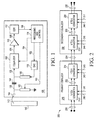
- FIG. 1 illustrates a simplified block diagram of a portion of a wireline receiver, according to an example embodiment
- FIG. 2 illustrates a simplified block diagram of an equalizer consisting of series-connected, primary and secondary equalizers, according to an example embodiment
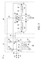
- FIG. 3 illustrates a circuit diagram of a primary equalizer, according to an example embodiment
- FIG. 4 illustrates a simplified, circuit diagram of a source degeneration impedance circuit, according to an example embodiment
- FIG. 5 illustrates a simplified, circuit diagram of a source degeneration impedance circuit, according to another example embodiment
- FIG. 6 illustrates a simplified, circuit diagram of a feedback impedance circuit, according to an example embodiment
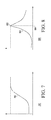
- FIG. 7 illustrates a graph of a transconductance-frequency transfer function for an equalizer with a source degeneration circuit that includes a non-zero resistance and a non-zero capacitance, in accordance with the prior art
- FIG. 8 illustrates a graph of a transconductance-frequency transfer function for an equalizer with a source degeneration circuit that includes an LC resonant circuit, according to an example embodiment.
- Embodiments include equalizers with resonant circuits that enable the gain-frequency response of the equalizers to be tailored to more effectively compensate for intersymbol interference (ISI) over a bandwidth of interest.
- An embodiment of a primary equalizer stage includes a voltage-to-current converter coupled in series with a current-to-voltage converter.
- the voltage-to-current converter converts a differential input voltage to a differential current, and includes a differential amplifier and a source degeneration circuit.
- the source degeneration circuit includes a resonant circuit that affects the gain-frequency response of the equalizer, in an embodiment.
- the current-to-voltage converter converts the differential current produced by the voltage-to-current converter to a differential output voltage.
- the current-to-voltage converter includes a pair of coupled inverters, each with a feedback circuit, and is current-biased with a current sink for differential operations.
- each feedback circuit also includes a resonant circuit that further affects the gain-frequency response of the equalizer, in an embodiment.
- the resonant circuits of either the source degeneration circuit or the feedback circuits may be replaced by non-resonant circuits.
- a further embodiment of an equalizer includes a secondary equalizer coupled in series with the primary equalizer, where the secondary equalizer functions as a swappable equalizer/limiter.
- source degeneration circuits and feedback circuits are discussed below.
- the source degeneration circuits and/or feedback circuits are described to include “resistors,” “capacitors,” and “inductors.” It is to be understood that any reference to a “resistor,” “capacitor” or “inductor” in the description or claims should be interpreted to mean either a discrete component (e.g., a single resistor, capacitor or inductor) or a circuit or network that includes multiple interconnected components of a particular type (e.g., a resistor circuit, capacitor circuit or inductor circuit). Similarly, references to a "resistor circuit,” a “capacitor circuit” or an “inductor circuit” in the description or claims may be interpreted to mean multiple interconnected components of a particular type or a single discrete component.
- FIG. 1 illustrates a simplified block diagram of a portion of a wireline receiver 100, according to an example embodiment.
- Receiver 100 includes variable impedance circuit 102, AC coupling capacitor 104, bias circuit 106, equalizer 108, buffer 110, clock and data recovery (CDR) circuit 112, and processing and control circuit 114.
- Receiver 100 receives an input signal 130 from an input transmission medium, which may include, for example, a printed circuit board (PCB) microstrip 140, wirebond 142, bond pad 144, and/or additional or different conductive structures (not illustrated) that comprise a wired transmission medium.
- PCB printed circuit board
- input signal 130 and other subsequently described data-bearing signals e.g., signals 132, 134, 136, 138
- these signals actually are differential signals, according to an embodiment.
- Variable impedance circuit 102 is configured to reduce reflections of the input signal 130 due to impedance mismatches between the input transmission medium and components at the input of receiver 100.
- the impedance of variable impedance circuit 102 may be adaptively adjusted through alteration of values of variable components within variable impedance circuit 102, where the adjustments may be conveyed in control signals 150 provided by processing and control circuit 114.
- Processing and control circuit 114 may calculate the adjustments based on analyses of feedback signals (e.g., signals 138 provided by CDR circuit 112).
- AC coupling capacitor 104 receives the input signal 130, and is configured to high pass filter the input signal in order to reduce out-of-band signal and noise components.
- An input bias is applied to the resulting, filtered input signal 132 by bias circuit 106, in order to minimize the input referred offset.
- the applied bias also may be controlled by processing and control circuit 114, through a control signal 152 that may be converted to an opposite magnitude of the input referred offset voltage at the equalizer input port by the digital-to-analog converter (DAC) 116 and bias circuit 106.
- DAC digital-to-analog converter
- the filtered input signal 132 is a coded signal (e.g., an 8 bit/10 bit coded signal).
- Equalizer 108 receives signal 132, and applies a transfer function to the signal 132 in order to adaptively compensate for signal losses imparted on the signal 132 by the transmission medium.
- embodiments of equalizer 108 are designed to more effectively compensate for intersymbol interference (ISI) than traditional equalizers, particularly at relatively high frequencies (e.g., frequencies up to and exceeding 5 gigahertz), thus enabling eye jitter to be reduced to levels that result in robust data detection by CDR circuit 112.
- ISI intersymbol interference
- Variable resistors e.g., resistor circuits
- variable capacitors e.g., varactors or capacitor circuits
- equalizer control signals 154 provided by processing and control circuit 114, as will be described in more detail later.
- Voltage buffer 110 comprises a unity-gain buffer amplifier, which substantially eliminates loading effects that may be present between the circuits.
- CDR circuit 112 receives the post-voltage-buffer, equalized signal 136, and generates a local clock from an approximate frequency reference, which is substantially phase-aligned with transitions in the data stream represented in equalized signal 136.
- the phase-aligned clock is used to make a correct data decision on the received, equalized signal 136, in order to produce a phase-aligned signal 138.
- Processing and control circuit 114 receives the phase-aligned signal 138, and is configured to detect the crossing point for each signal pulse (e.g., to detect the signal at the bit-cell boundaries). More particularly, periodically and within a certain time frame from receiving a portion of the phase-aligned signal 138, processing and control circuit 114 analyzes the pulse-edge distribution of the phase-aligned signal 138, where a "pulse-edge" may correspond to a rising or falling edge. In the context of that analysis, processing and control circuit 114 determines the nominal zero-crossing locations of pulses that contain different numbers of bits (e.g., pulse widths of 1-bit, 2-bits, .. 5-bits, and so on).
- processing and control circuit 114 determines whether the zero-crossing locations among the various bit pulses indicate whether the equalizer is being operated at over or under equalization conditions. Via control signal 154, processing and control circuit 114 may then adjust various component values within equalizer 108, which bring the equalizer conditions within a more optimal range. According to an embodiment and as will be discussed in more detail later, decoder logic circuitry (not illustrated) may be employed to control various tunable resistors and/or capacitors of equalizer 108, in order to adjust the high-frequency gain response.
- FIG. 2 illustrates a simplified block diagram of an equalizer 200 (e.g., equalizer 108, FIG. 1 ), which includes series-connected, primary and secondary equalizer stages 210, 220, according to an example embodiment.
- Primary equalizer stage 210 is configured to provide the primary equalization for the equalizer 200
- secondary equalizer stage 220 is configured to function as a swappable equalizer/limiter, which enhances the subsequent equalization gain and/or functions as a limiter, when appropriate.
- Primary equalizer stage 210 includes a first voltage-to-current (V-to-I) converter 212 coupled with a first current-to-voltage (I-to-V) converter 214.
- the first V-to-I converter 212 receives a differential input voltage signal 230 (e.g., signal 132, FIG. 1 ), and converts it into a differential current signal 232.
- first V-to-I converter 212 includes a differential amplifier with source degeneration impedance, where the source degeneration impedance is provided with a source degeneration impedance circuit (e.g., circuit 320, FIG. 3 ).
- the source degeneration impedance circuit may include a variable resistor (e.g., a resistor circuit) in parallel with a series inductor-capacitor (LC) circuit, where the series LC circuit includes one or more inductors in series with one or more variable capacitors (e.g., varactors or capacitor circuits), in an embodiment.
- the resistance of the source degeneration impedance circuit may be varied based on a resistance control signal 241 provided by a control component of the system (e.g., equalizer control signal 154 provided by processing and control circuit 114, FIG. 1 ), in order to adjust the signal gain applied by primary equalizer 210.
- the capacitance of the variable capacitors may be varied based on a capacitance control signal 240 provided by a control component of the system (e.g., equalizer control signal 154 provided by processing and control circuit 114, FIG. 1 ), in order to affect the frequency response of the V-to-I converter 212.
- a control component of the system e.g., equalizer control signal 154 provided by processing and control circuit 114, FIG. 1
- first I-to-V converter 214 receives the differential current signal 232 produced by the first V-to-I converter 212, and converts it into a differential voltage signal 234.
- first I-to-V converter 214 includes a pair of inverters (e.g., CMOS inverters comprising transistors 356, 358, 360, 362, FIG. 3 ), feedback impedance circuits (e.g., feedback impedance circuits 364, 366, FIG. 3 ), and a tail current sink (e.g., tail current sink 374, FIG. 3 ) to support differential operations for the pair of inverters and the feedback impedance circuits, in an embodiment.
- inverters e.g., CMOS inverters comprising transistors 356, 358, 360, 362, FIG. 3
- feedback impedance circuits e.g., feedback impedance circuits 364, 366, FIG. 3
- tail current sink e.g., tail current sink 374, FIG. 3
- the resistances of the feedback impedance circuits may be varied based on a resistance control signal 242 provided by a control component of the system (e.g., equalizer control signal 154 provided by processing and control circuit 114, FIG. 1 ), in order to adjust the signal gain applied by primary equalizer 210.
- a control component of the system e.g., equalizer control signal 154 provided by processing and control circuit 114, FIG. 1
- the capacitances of the variable capacitors may be varied based on a capacitance control signal 243 provided by the control component of the system.
- secondary equalizer stage 220 may function as a swappable equalizer/limiter. This means that secondary equalizer stage 220 may either enhance the signal gain further in the selected high-frequency band (e.g., when the voltage signal 234 produced by the primary equalizer stage 210 has insufficiently steep pulse-edge slopes at its waveform or has a lower magnitude of high-frequency spectrum in the frequency domain, which indicates a condition of under-equalization), or may function as a limiter circuit that clips the signal (e.g., when the voltage signal 234 produced by the primary equalizer stage 210 has sufficiently steep pulse-edge slopes at its waveform or a sufficiently large magnitude of high-frequency spectrum in the frequency domain, which indicates a condition of over-equalization).
- processing and control circuit 114 evaluates the conditions indicated by phase-aligned signal 138 to determine whether equalizer 108 is providing over- or under- equalization, and based on that determination, the processing and control circuit 114 may cause the functional modes of secondary equalizer stage 220 to swap between either an extended equalizer stage (when a condition of under-equalization is detected) or a limiter circuit (when a condition of over-equalization is detected).
- Secondary equalizer stage 220 is coupled in series with the output of the primary equalizer stage 210, and includes a second V-to-I converter 222 and a second I-to-V converter 224.
- the second V-to-I converter 222 receives the differential voltage signal 234, and converts it into a differential current signal 236.
- the second V-to-I converter 222 may be configured substantially the same as or differently from the first V-to-I converter 212.
- the second V-to-I converter 222 is similar to the first V-to-I converter 212, in that the second V-to-I converter 222 also includes a differential amplifier and a source degeneration impedance circuit with a variable resistor in parallel with one or more variable capacitors.
- the source degeneration impedance circuit of the second V-to-I converter 222 may or may not include one or more inductors in series with the one or more variable capacitors. Either way, the capacitance of the variable capacitor(s) may be varied based on a capacitance control signal 244 provided by a control component of the system (e.g., equalizer control signal 154 provided by processing and control circuit 114, FIG. 1 ), in order to affect the frequency response of the V-to-I converter 222.
- the resistance of the source degeneration impedance circuit may be varied based on a resistance control signal 245 provided by a control component of the system (e.g., equalizer control signal 154 provided by processing and control circuit 114, FIG. 1 ), in order to adjust the signal gain applied by secondary equalizer 220.
- the second I-to-V converter 224 receives the differential current signal 236 produced by the second V-to-I converter 222, and converts it into a differential output voltage signal 238. Differential output voltage signal 238 corresponds to the output signal of the equalizer 200 (e.g., equalized signal 134, FIG. 1 ), in an embodiment.
- the second I-to-V converter 224 may be configured substantially the same as or differently from the first I-to-V converter 214.
- the second I-to-V converter 224 also includes a pair of inverters (e.g., CMOS inverters) and either feedback resistor circuits or feedback impedance circuits (referred to generally as "feedback circuits").
- the resistances of the feedback resistor circuits may be varied based on a resistance control signal 246 provided by a control component of the system (e.g., equalizer control signal 154 provided by processing and control circuit 114, FIG. 1 ), in order to adjust the signal gain applied by secondary equalizer 220.
- a control component of the system e.g., equalizer control signal 154 provided by processing and control circuit 114, FIG. 1
- the capacitances of the variable capacitors may be varied based on a capacitance control signal 247 provided by the control component of the system.
- the second I-to-V converter 224 also may include a tail current sink (e.g., tail current sink 374, FIG. 3 ) to support differential operations for the pair of inverters and the feedback circuits.
- FIG. 3 illustrates a circuit diagram of a primary equalizer 300 (e.g., primary equalizer 210, FIG. 2 ), according to an example embodiment.
- Primary equalizer 300 includes a V-to-I converter 310 (e.g., V-to-I converter 212, FIG. 2 ) connected in series with an I-to-V converter 350 (e.g., I-to-V converter 214, FIG. 2 ).
- V-to-I converter 310 is configured to convert a differential input voltage signal 340 (e.g., signal 132, FIG. 1 or 230, FIG. 2 ) into a differential current signal 342 (e.g., signal 232, FIG. 2 ).
- V-to-I converter 310 includes a non-inverting input 312, an inverting input 314, a differential amplifier circuit comprised of at least a pair of transistors 316, 318, a source degeneration impedance circuit 320, an inverting output 322, a non-inverting output 324, a first current source 326, a second current source 328, a first current sink 330, and a second current sink 332, in an embodiment.
- First current sink 330 and second current sink 332 draw power from source voltage 338 (e.g., Vdd).
- p-type current sources may be used for the first and second current sources 326, 328, which may increase the headroom of the equalizer 300.
- the first current source 326 and the second current source 328 may be replaced with a current mirror circuit (e.g., current mirror circuit 402, FIG. 4 ).
- transistors 316, 318 of the differential amplifier sub-circuit are coupled between the non-inverting input 312, the inverting input 314, the inverting output 322, and the non-inverting output 324, as shown in FIG. 3 .
- transistors 316, 318 are field effect transistors (FETs) (e.g., metal-oxide semiconductor FETs (MOSFETs))
- FETs field effect transistors
- MOSFETs metal-oxide semiconductor FETs
- the gates of transistors 316, 318 are coupled to the non-inverting input 312 and the inverting input 314, respectively, and the drains of transistors 316, 318 are coupled with the first current source 326 and the second current source 328, respectively.
- the sources of transistors 316, 318 are coupled to the first current sink 330 and the second current sink 332, respectively, and also are coupled through source degeneration impedance circuit 320.
- the source degeneration impedance circuit 320 is configured to control the gain-frequency response of the V-to-I converter 310.
- the source degeneration impedance circuit 320 includes a series inductor-capacitor (LC) resonant circuit 334, and a resistor (R) circuit 336, where the resistor circuit 336 is coupled in parallel with the series LC resonant circuit 334.
- LC inductor-capacitor
- R resistor
- the impedance of the LC resonant circuit 334 becomes very small (e.g., resembling a short circuit), and the transconductance of the V-to-I converter 310 is maximized (e.g., the gain of the V-to-I converter 310 is maximized).
- FIG. 4 illustrates a simplified, circuit diagram of a source degeneration impedance circuit 400 (e.g., source degeneration impedance circuit 320, FIG. 3 ), according to an example embodiment.
- Circuit 400 includes a first inductor 404 (with a series parasitic resistance represented by resistor 402), a capacitor 406, and a second inductor 408 (with a series parasitic resistance represented by resistor 410), connected in series in the above-listed order.
- a resistor 412 is connected in parallel with the series-connected inductor 404, capacitor 406, and inductor 408.
- capacitor 406 is a variable capacitor (e.g., controllable via capacitance control signal 240, FIG. 2 ), although capacitor 406 may have a fixed capacitance, in an alternate embodiment.
- resistor 412 is a variable resistor (e.g., controllable via resistance control signal 241, FIG. 2 ). In alternate embodiments, either or both capacitor 406 and resistor 412 may have a fixed capacitance or resistance, respectively. In still other alternate embodiments, either the first or second inductors 404, 408 may be excluded from the circuit.
- FIG. 5 illustrates a simplified, circuit diagram of a source degeneration impedance circuit 500 (e.g., source degeneration impedance circuit 320, FIG. 3 ), according to another example embodiment.
- Circuit 500 includes a first capacitor 502, an inductor 506 (with a series parasitic resistance represented by resistor 504), and a second capacitor 508, connected in series in the above-listed order.
- a resistor 510 is connected in parallel with the series-connected capacitor 502, inductor 506, and capacitor 508.
- capacitors 502, 508 are a variable capacitor (e.g., controllable via capacitance control signal 240, FIG. 2 ), although one or both of capacitors 502, 508 may have a fixed capacitance, in alternate embodiments.
- resistor 510 is a variable resistor (e.g., controllable via resistance control signal 241, FIG. 2 ).
- either or both capacitors 502, 508 and/or resistor 510 may have a fixed capacitances or resistance, respectively.
- inductor 506 may be excluded from the circuit.
- source degeneration impedance circuits are illustrated in conjunction with FIGs 4 and 5 , above, it is to be understood that the circuit configurations provided in FIGs 4 and 5 are provided for example purposes only, and that other embodiments may employ differently configured LC resonant circuits.
- discrete capacitors, inductors, and resistors may be depicted in conjunction with FIGs 4-6 , each of the illustrated discrete components may be implemented with circuits of series and/or parallel connected components.
- the source degeneration impedance circuits discussed above in conjunction with FIGs 4-5 each include one or more inductive components.
- source degeneration impedance circuit 320 may be replaced with a source degeneration circuit that does not include any inductive components.
- the capacitance of the LC resonant circuit 334 is adjustable (e.g., via capacitance control signal 240, FIG. 2 ), which enables the equalizer transfer function of the gain-frequency response to be tuned. Accordingly, the LC resonant circuit 334 may be tuned so that its resonant frequency corresponds with the bandwidth of the communication protocol being implemented by the system, at the time.
- the capacitance control signal e.g., capacitance control signal 240, FIG. 2
- the capacitance control signal is comprised of two bits, the values of which may correspond to four distinct capacitance values for the capacitance of the LC resonant circuit 334.
- the capacitance control signal may include more or fewer bits, which may correspond to more or fewer distinct capacitance values.
- the I-to-V converter stage 350 is configured to convert the differential current signal 342 produced by the V-to-I converter 310 into a differential output voltage signal 344.
- I-to-V converter 350 includes an inverting input 352, a non-inverting input 354, a first inverter comprising first and second transistors 356, 358 (e.g., a CMOS inverter), a second inverter comprising third and fourth transistors 360, 362 (e.g., also a CMOS inverter), first feedback impedance circuit 364, second feedback impedance circuit 366, a non-inverting output 370, an inverting output 372, and a tail current sink 374, in an embodiment.
- the transistors 356, 358, 360, 362 of the first and second inverters are coupled between the inverting input 352, the non-inverting input 354, the non-inverting output 370, and the inverting output 372, as shown in FIG. 3 .
- transistors 356, 358, 360, 362 are MOSFETs
- the gates of transistors 356, 358 are coupled to the inverting input 352, and the gates of transistors 360, 362 are coupled to the non-inverting input 354.
- the drains of transistors 356, 360 are coupled with the source voltage 338, and the drains of transistors 358, 362 are coupled with tail current sink 374.
- the sources of transistors 356, 358 are coupled together and to the non-inverting output 370, and the sources of transistors 360, 362 are coupled together and to the inverting output 372.
- Tail current sink 374 provides a bias current for both coupled inverters and the related feedback circuits (e.g. transistors 356, 358, 360, and 362, and circuits 364 and 366), in order to support differential circuit operations for higher switching speeds. Tail current sink 374 also may enhance the noise immunity capacity against power supply noise (e.g., noise from source voltage 338 or ground) and the input common-mode noise (e.g., common-mode noise at both inputs 352 and 354).
- power supply noise e.g., noise from source voltage 338 or ground
- common-mode noise e.g., common-mode noise at both inputs 352 and 354
- First feedback impedance circuit 364 is coupled across the gates and sources of transistors 356, 358, and thus between the inverting input 352 and the non-inverting output 370.
- second feedback impedance circuit 366 is coupled across the gates and sources of transistors 360, 362, and thus between the non-inverting input 354 and the inverting output 372.
- the first and second feedback impedance circuits 364, 366 are configured to enhance the gain and bandwidth performance of primary equalizer 300.
- each of feedback impedance circuits 364, 366 includes an impedance (Z) circuit 380, 382 coupled in series with a resistor (R) circuit 386, 388.
- the impedance circuits 380, 382 may include an inductance circuit, a capacitance circuit, or a combined LC circuit, in various embodiments.
- the impedance circuits 380, 382 each may include a parallel connected inductor circuit and capacitor circuit, connected in series with a resistor circuit, as will be described in conjunction with FIG. 6 .
- each of the impedance circuits 380, 382 may include an inductor circuit in series with a resistor circuit (i.e., without a capacitor circuit).
- the impedance circuits 380, 382 may be replaced with a resistor circuit.
- FIG. 6 illustrates a simplified, circuit diagram of a feedback impedance circuit 600 (e.g., either or both of feedback impedance circuits 364, 366, FIG. 3 ), according to an example embodiment.
- Circuit 600 includes an inductor 602 (with a series parasitic resistance represented by resistor 604) connected in parallel with a capacitor 606, and a resistor 608 connected in series with the parallel-connected inductor 602 and capacitor 606.
- resistor 608 is a variable resistor (e.g., controllable via resistance control signal 242, FIG. 2 )
- capacitor 606 is a variable capacitor (e.g., controllable via capacitance control signal 243, FIG. 2 ).
- either or both capacitor 606 and resistor 608 may have a fixed capacitance or resistance, respectively.
- the impedances of the impedance circuits 380, 382 become very large (e.g., resembling an open circuit), and the transimpedance of the I-to-V converter 350 is maximized (e.g., the gain of the I-to-V converter 350 is maximized).
- the extra impedance provided by impedance circuits 380, 382 will boost up the overall AC gain of the equalizer 300.
- the resistances of the resistor circuits 386, 388 are adjustable (e.g., via resistance control signal 242, FIG. 2 ).
- the impedance circuits 380, 382 include capacitors
- the capacitors also may be adjustable (e.g., via capacitance control signal 243, FIG. 2 ).
- the adjustability of the resistor and impedance circuits 380, 382, 386, 3 88, once again, enables the equalizer transfer function of the gain-frequency response to be further tuned. Similar to LC circuit 334, the impedance circuits 380, 382 may be tuned so that their resonant frequencies correspond with the bandwidth of the communication protocol being implemented by the system, at the time.
- the capacitance control signal (e.g., capacitance control signal 243, FIG. 2 ) is comprised of two bits, the values of which may correspond to four distinct capacitance values for the capacitance of the impedance circuits 380, 382.
- the resistance control signal (e.g., resistance control signal 242, FIG. 2 ) is comprised of four bits, the values of which may correspond to sixteen distinct resistance values for the resistance of the resistor circuits 386, 388.
- the capacitance and/or resistance control signals may include more or fewer bits, which may correspond to more or fewer distinct capacitance and resistance values.
- the equalizer's gain-frequency transfer function may be "shaped" to match the communication channel's gain (loss) transfer characteristic.
- the peak gain may be set to a desired frequency, and minimum gains at lower frequencies may be defined.
- the total degeneration-impedance becomes a minimum at the resonant frequency of the LC resonant circuit 334. This enables the V-to-I converter 310 to generate a desired gain-frequency transfer function for the I-to-V converter 350.
- the peak gain may be set to a desired frequency based on the capacitance of the feedback impedance circuits 364, 366, and the resistance of the feedback impedance circuits 364, 366 may be controlled to define the minimum gain at lower frequencies.
- FIG. 7 illustrates a graph 700 of a transconductance-frequency transfer function 702 for an equalizer with a source degeneration circuit that includes a non-zero resistance and a non-zero capacitance (i.e., the source degeneration circuit does not include an inductance circuit), in accordance with the prior art.
- frequency is represented along the horizontal axis
- transconductances represented along the vertical axis.
- the transfer function 702 shows, the non-zero resistance attenuates an input signal at relatively low frequencies, and the non-zero capacitance allows the signal to be passed through the equalizer at relatively high frequencies.
- FIG. 8 illustrates a graph 800 of a transconductance-frequency transfer function 802 for an equalizer with a source degeneration circuit (e.g., source degeneration circuit 320, FIG. 3 ) that includes an LC resonant circuit (e.g., LC resonant circuit 334, FIG. 3 ), according to an example embodiment.
- a source degeneration circuit e.g., source degeneration circuit 320, FIG. 3
- LC resonant circuit e.g., LC resonant circuit 334, FIG. 3
- the inductance present in the LC resonant circuit causes a transfer function in which the transconductance remains the same as that of the differential pair (e.g., transistors 316 and 318) without source degeneration reduction at the resonant frequency 804 of the LC resonant circuit, which results in a peak 806 in the transfer function at the resonant frequency 804. On either side of the peak 806, the gain is attenuated.
- the differential pair e.g., transistors 316 and 318
- An embodiment of an equalizer includes a voltage-to-current converter and a current-to-voltage converter.
- the voltage-to-current converter is configured to convert a differential input voltage to a differential current, and includes a differential amplifier having a first transistor and a second transistor, and a first source degeneration circuit coupled between the first transistor and the second transistor.
- the first source degeneration circuit includes a first resonant circuit.
- the current-to-voltage converter is coupled to the voltage-to-current converter, and is configured to convert the differential current to a differential output voltage.
- the current-to-voltage converter includes a first inverter with a first feedback circuit and a second inverter coupled to the first inverter, which includes a second feedback circuit.
- the first feedback circuit includes a second resonant circuit
- the second feedback circuit includes a third resonant circuit.
- an equalizer also includes a voltage-to-current converter and a current-to-voltage converter.
- the voltage-to-current converter is configured to convert a differential input voltage to a differential current, and includes a differential amplifier having a first transistor and a second transistor, and a first source degeneration circuit coupled between the first transistor and the second transistor.
- the first source degeneration circuit includes a first resonant circuit.
- the current-to-voltage converter is coupled to the voltage-to-current converter, and is configured to convert the differential current to a differential output voltage.
- the current-to-voltage converter includes a first inverter with a first feedback circuit, and a second inverter coupled to the first inverter, which includes a second feedback circuit.
- an equalizer also includes a voltage-to-current converter and a current-to-voltage converter.
- the voltage-to-current converter is configured to convert a differential input voltage to a differential current, and includes a differential amplifier having a first transistor and a second transistor, and a first source degeneration circuit coupled between the first transistor and the second transistor.
- the current-to-voltage converter is coupled to the voltage-to-current converter, and is configured to convert the differential current to a differential output voltage.
- the current-to-voltage converter includes a first inverter with a first feedback circuit, and a second inverter coupled to the first inverter with a second feedback circuit.
- the first feedback circuit includes a first resonant circuit
- the second feedback circuit includes a second resonant circuit.
Landscapes
- Engineering & Computer Science (AREA)
- Computer Networks & Wireless Communication (AREA)
- Signal Processing (AREA)
- Amplifiers (AREA)
Abstract
Description
- Embodiments relate to differential equalizers for wireline communications, and more particularly to differential equalizers that include source degeneration circuits and feedback circuits.
- In wireline communications, a received signal may be distorted due to intersymbol interference (ISI) from the signal channels. ISI results from dielectric losses and frequency-dependent signal losses (due to the skin effect) that occur along the transmission medium (e.g., printed circuit board (PCB) microstrips, cables, coaxial connecters, and so on). ISI typically causes significant eye jitter, which makes it more difficult for a receiver to synchronize in a manner that results in reliable clock and data recovery.
- In some wireline receivers, adaptive equalization circuits (or "equalizers") are implemented to compensate for ISI. An equalizer receives an ISI-distorted signal from the transmission medium, and attempts to compensate for losses over the signal bandwidth, in order to reduce the eye jitter to an acceptable level. More particularly, an equalizer has a gain-versus-frequency transfer function which, ideally, is an inverse of the gain (loss)-versus-frequency characteristic of the signal channel. Accordingly, the equalizer may compensate for the loss imparted by the signal channel by applying appropriate gains to the received signal across the signal bandwidth. Because the loss characteristics of a channel tend to increase as the transmission frequency increases, a well designed equalizer should have higher gain-versus-frequency slope characteristics at higher frequencies.
- Although traditional equalizers designed for lower-frequency transmissions have adequately compensated for ISI at those lower frequencies, these equalizers were not designed to perform robustly for the higher frequency communications that are becoming increasingly more prevalent and desired. Accordingly, most traditional equalizers are not capable of adequately compensating for higher ISI inherent in increasingly higher frequency communications.
- Some more contemporary equalizer designs have attempted to tackle ISI issues inherent in higher-frequency communications. For example, some newer equalizers include multiple branches of cascaded "differentiator circuits" to composite an equalizer. However, the capacitive parasitic of the multi-parallel stages limits the high-speed capacity. In addition, these equalizers typically use many gain stages, which significantly increase a receiver's power consumption, particularly at high frequencies. Other undesirable effects also may be inherent in some new equalizer designs (e.g., inadequate or inconsistent gain over the bandwidth of interest, sensitive AC gain response, frequency limitations, and so on). Accordingly, designers continue to strive to develop relatively low-power, adaptive equalization circuits that can provide adequate ISI compensation at increasingly higher transmission frequencies.
-
FIG. 1 illustrates a simplified block diagram of a portion of a wireline receiver, according to an example embodiment; -
FIG. 2 illustrates a simplified block diagram of an equalizer consisting of series-connected, primary and secondary equalizers, according to an example embodiment; -
FIG. 3 illustrates a circuit diagram of a primary equalizer, according to an example embodiment; -
FIG. 4 illustrates a simplified, circuit diagram of a source degeneration impedance circuit, according to an example embodiment; -
FIG. 5 illustrates a simplified, circuit diagram of a source degeneration impedance circuit, according to another example embodiment; -
FIG. 6 illustrates a simplified, circuit diagram of a feedback impedance circuit, according to an example embodiment; -
FIG. 7 illustrates a graph of a transconductance-frequency transfer function for an equalizer with a source degeneration circuit that includes a non-zero resistance and a non-zero capacitance, in accordance with the prior art; and -
FIG. 8 illustrates a graph of a transconductance-frequency transfer function for an equalizer with a source degeneration circuit that includes an LC resonant circuit, according to an example embodiment. - Embodiments include equalizers with resonant circuits that enable the gain-frequency response of the equalizers to be tailored to more effectively compensate for intersymbol interference (ISI) over a bandwidth of interest. An embodiment of a primary equalizer stage includes a voltage-to-current converter coupled in series with a current-to-voltage converter. The voltage-to-current converter converts a differential input voltage to a differential current, and includes a differential amplifier and a source degeneration circuit. As will be described in more detail below, the source degeneration circuit includes a resonant circuit that affects the gain-frequency response of the equalizer, in an embodiment. The current-to-voltage converter converts the differential current produced by the voltage-to-current converter to a differential output voltage. The current-to-voltage converter includes a pair of coupled inverters, each with a feedback circuit, and is current-biased with a current sink for differential operations. As will also be described in more detail below, each feedback circuit also includes a resonant circuit that further affects the gain-frequency response of the equalizer, in an embodiment. In alternate embodiments, the resonant circuits of either the source degeneration circuit or the feedback circuits may be replaced by non-resonant circuits. A further embodiment of an equalizer includes a secondary equalizer coupled in series with the primary equalizer, where the secondary equalizer functions as a swappable equalizer/limiter.
- Various embodiments of source degeneration circuits and feedback circuits are discussed below. In some of the below discussed embodiments, the source degeneration circuits and/or feedback circuits are described to include "resistors," "capacitors," and "inductors." It is to be understood that any reference to a "resistor," "capacitor" or "inductor" in the description or claims should be interpreted to mean either a discrete component (e.g., a single resistor, capacitor or inductor) or a circuit or network that includes multiple interconnected components of a particular type (e.g., a resistor circuit, capacitor circuit or inductor circuit). Similarly, references to a "resistor circuit," a "capacitor circuit" or an "inductor circuit" in the description or claims may be interpreted to mean multiple interconnected components of a particular type or a single discrete component.
-
FIG. 1 illustrates a simplified block diagram of a portion of awireline receiver 100, according to an example embodiment.Receiver 100 includesvariable impedance circuit 102,AC coupling capacitor 104,bias circuit 106,equalizer 108,buffer 110, clock and data recovery (CDR)circuit 112, and processing andcontrol circuit 114.Receiver 100 receives aninput signal 130 from an input transmission medium, which may include, for example, a printed circuit board (PCB)microstrip 140,wirebond 142,bond pad 144, and/or additional or different conductive structures (not illustrated) that comprise a wired transmission medium. Althoughinput signal 130 and other subsequently described data-bearing signals (e.g.,signals -
Variable impedance circuit 102 is configured to reduce reflections of theinput signal 130 due to impedance mismatches between the input transmission medium and components at the input ofreceiver 100. The impedance ofvariable impedance circuit 102 may be adaptively adjusted through alteration of values of variable components withinvariable impedance circuit 102, where the adjustments may be conveyed incontrol signals 150 provided by processing andcontrol circuit 114. Processing andcontrol circuit 114 may calculate the adjustments based on analyses of feedback signals (e.g.,signals 138 provided by CDR circuit 112). -
AC coupling capacitor 104 receives theinput signal 130, and is configured to high pass filter the input signal in order to reduce out-of-band signal and noise components. An input bias is applied to the resulting, filteredinput signal 132 bybias circuit 106, in order to minimize the input referred offset. The applied bias also may be controlled by processing andcontrol circuit 114, through acontrol signal 152 that may be converted to an opposite magnitude of the input referred offset voltage at the equalizer input port by the digital-to-analog converter (DAC) 116 andbias circuit 106. - According to an embodiment, the filtered
input signal 132 is a coded signal (e.g., an 8 bit/10 bit coded signal).Equalizer 108 receivessignal 132, and applies a transfer function to thesignal 132 in order to adaptively compensate for signal losses imparted on thesignal 132 by the transmission medium. As will be described in more detail below, embodiments ofequalizer 108 are designed to more effectively compensate for intersymbol interference (ISI) than traditional equalizers, particularly at relatively high frequencies (e.g., frequencies up to and exceeding 5 gigahertz), thus enabling eye jitter to be reduced to levels that result in robust data detection byCDR circuit 112. Variable resistors (e.g., resistor circuits) and variable capacitors (e.g., varactors or capacitor circuits) withinequalizer 108, which affect the equalizer gain-frequency response, may be adjusted byequalizer control signals 154 provided by processing andcontrol circuit 114, as will be described in more detail later. The configuration and controllability ofequalizer 108 enables a reduction in the eye jitter of the filteredinput signal 132 to a level that enablesCDR circuit 112 to perform its operations robustly. -
Voltage buffer 110 comprises a unity-gain buffer amplifier, which substantially eliminates loading effects that may be present between the circuits.CDR circuit 112 receives the post-voltage-buffer, equalizedsignal 136, and generates a local clock from an approximate frequency reference, which is substantially phase-aligned with transitions in the data stream represented in equalizedsignal 136. The phase-aligned clock, in turn, is used to make a correct data decision on the received, equalizedsignal 136, in order to produce a phase-alignedsignal 138. - Processing and
control circuit 114 receives the phase-alignedsignal 138, and is configured to detect the crossing point for each signal pulse (e.g., to detect the signal at the bit-cell boundaries). More particularly, periodically and within a certain time frame from receiving a portion of the phase-alignedsignal 138, processing andcontrol circuit 114 analyzes the pulse-edge distribution of the phase-alignedsignal 138, where a "pulse-edge" may correspond to a rising or falling edge. In the context of that analysis, processing andcontrol circuit 114 determines the nominal zero-crossing locations of pulses that contain different numbers of bits (e.g., pulse widths of 1-bit, 2-bits, .. 5-bits, and so on). During subsequent comparing operations, processing andcontrol circuit 114 determines whether the zero-crossing locations among the various bit pulses indicate whether the equalizer is being operated at over or under equalization conditions. Viacontrol signal 154, processing andcontrol circuit 114 may then adjust various component values withinequalizer 108, which bring the equalizer conditions within a more optimal range. According to an embodiment and as will be discussed in more detail later, decoder logic circuitry (not illustrated) may be employed to control various tunable resistors and/or capacitors ofequalizer 108, in order to adjust the high-frequency gain response. -
FIG. 2 illustrates a simplified block diagram of an equalizer 200 (e.g.,equalizer 108,FIG. 1 ), which includes series-connected, primary and secondary equalizer stages 210, 220, according to an example embodiment.Primary equalizer stage 210 is configured to provide the primary equalization for theequalizer 200, andsecondary equalizer stage 220 is configured to function as a swappable equalizer/limiter, which enhances the subsequent equalization gain and/or functions as a limiter, when appropriate. -
Primary equalizer stage 210 includes a first voltage-to-current (V-to-I)converter 212 coupled with a first current-to-voltage (I-to-V)converter 214. The first V-to-I converter 212 receives a differential input voltage signal 230 (e.g., signal 132,FIG. 1 ), and converts it into a differentialcurrent signal 232. As will be described in more detail in conjunction withFIG. 3 , first V-to-I converter 212 includes a differential amplifier with source degeneration impedance, where the source degeneration impedance is provided with a source degeneration impedance circuit (e.g.,circuit 320,FIG. 3 ). The source degeneration impedance circuit may include a variable resistor (e.g., a resistor circuit) in parallel with a series inductor-capacitor (LC) circuit, where the series LC circuit includes one or more inductors in series with one or more variable capacitors (e.g., varactors or capacitor circuits), in an embodiment. The resistance of the source degeneration impedance circuit may be varied based on aresistance control signal 241 provided by a control component of the system (e.g.,equalizer control signal 154 provided by processing andcontrol circuit 114,FIG. 1 ), in order to adjust the signal gain applied byprimary equalizer 210. In addition, the capacitance of the variable capacitors may be varied based on a capacitance control signal 240 provided by a control component of the system (e.g.,equalizer control signal 154 provided by processing andcontrol circuit 114,FIG. 1 ), in order to affect the frequency response of the V-to-I converter 212. - The first I-to-
V converter 214 receives the differentialcurrent signal 232 produced by the first V-to-I converter 212, and converts it into adifferential voltage signal 234. As will be also described in more detail in conjunction withFIG. 3 , first I-to-V converter 214 includes a pair of inverters (e.g., CMOSinverters comprising transistors FIG. 3 ), feedback impedance circuits (e.g.,feedback impedance circuits FIG. 3 ), and a tail current sink (e.g., tailcurrent sink 374,FIG. 3 ) to support differential operations for the pair of inverters and the feedback impedance circuits, in an embodiment. The resistances of the feedback impedance circuits may be varied based on a resistance control signal 242 provided by a control component of the system (e.g.,equalizer control signal 154 provided by processing andcontrol circuit 114,FIG. 1 ), in order to adjust the signal gain applied byprimary equalizer 210. In addition, in embodiments in which the feedback impedance circuits include variable capacitors, the capacitances of the variable capacitors may be varied based on acapacitance control signal 243 provided by the control component of the system. - As mentioned above,
secondary equalizer stage 220 may function as a swappable equalizer/limiter. This means thatsecondary equalizer stage 220 may either enhance the signal gain further in the selected high-frequency band (e.g., when thevoltage signal 234 produced by theprimary equalizer stage 210 has insufficiently steep pulse-edge slopes at its waveform or has a lower magnitude of high-frequency spectrum in the frequency domain, which indicates a condition of under-equalization), or may function as a limiter circuit that clips the signal (e.g., when thevoltage signal 234 produced by theprimary equalizer stage 210 has sufficiently steep pulse-edge slopes at its waveform or a sufficiently large magnitude of high-frequency spectrum in the frequency domain, which indicates a condition of over-equalization). As mentioned previously, processing andcontrol circuit 114 evaluates the conditions indicated by phase-alignedsignal 138 to determine whetherequalizer 108 is providing over- or under- equalization, and based on that determination, the processing andcontrol circuit 114 may cause the functional modes ofsecondary equalizer stage 220 to swap between either an extended equalizer stage (when a condition of under-equalization is detected) or a limiter circuit (when a condition of over-equalization is detected). -
Secondary equalizer stage 220 is coupled in series with the output of theprimary equalizer stage 210, and includes a second V-to-I converter 222 and a second I-to-V converter 224. The second V-to-I converter 222 receives thedifferential voltage signal 234, and converts it into a differentialcurrent signal 236. The second V-to-I converter 222 may be configured substantially the same as or differently from the first V-to-I converter 212. In an embodiment, the second V-to-I converter 222 is similar to the first V-to-I converter 212, in that the second V-to-I converter 222 also includes a differential amplifier and a source degeneration impedance circuit with a variable resistor in parallel with one or more variable capacitors. However, the source degeneration impedance circuit of the second V-to-I converter 222 may or may not include one or more inductors in series with the one or more variable capacitors. Either way, the capacitance of the variable capacitor(s) may be varied based on acapacitance control signal 244 provided by a control component of the system (e.g.,equalizer control signal 154 provided by processing andcontrol circuit 114,FIG. 1 ), in order to affect the frequency response of the V-to-I converter 222. In addition, in an embodiment, the resistance of the source degeneration impedance circuit may be varied based on aresistance control signal 245 provided by a control component of the system (e.g.,equalizer control signal 154 provided by processing andcontrol circuit 114,FIG. 1 ), in order to adjust the signal gain applied bysecondary equalizer 220. - The second I-to-
V converter 224 receives the differentialcurrent signal 236 produced by the second V-to-I converter 222, and converts it into a differentialoutput voltage signal 238. Differentialoutput voltage signal 238 corresponds to the output signal of the equalizer 200 (e.g., equalizedsignal 134,FIG. 1 ), in an embodiment. The second I-to-V converter 224 may be configured substantially the same as or differently from the first I-to-V converter 214. In an embodiment, the second I-to-V converter 224 also includes a pair of inverters (e.g., CMOS inverters) and either feedback resistor circuits or feedback impedance circuits (referred to generally as "feedback circuits"). In the former embodiment, the resistances of the feedback resistor circuits may be varied based on a resistance control signal 246 provided by a control component of the system (e.g.,equalizer control signal 154 provided by processing andcontrol circuit 114,FIG. 1 ), in order to adjust the signal gain applied bysecondary equalizer 220. In addition, in embodiments in which feedback impedance circuits with variable capacitors are implemented in the second I-to-V converter 224, the capacitances of the variable capacitors may be varied based on acapacitance control signal 247 provided by the control component of the system. The second I-to-V converter 224 also may include a tail current sink (e.g., tailcurrent sink 374,FIG. 3 ) to support differential operations for the pair of inverters and the feedback circuits. -
FIG. 3 illustrates a circuit diagram of a primary equalizer 300 (e.g.,primary equalizer 210,FIG. 2 ), according to an example embodiment.Primary equalizer 300 includes a V-to-I converter 310 (e.g., V-to-I converter 212,FIG. 2 ) connected in series with an I-to-V converter 350 (e.g., I-to-V converter 214,FIG. 2 ). As discussed previously, V-to-I converter 310 is configured to convert a differential input voltage signal 340 (e.g., signal 132,FIG. 1 or 230,FIG. 2 ) into a differential current signal 342 (e.g., signal 232,FIG. 2 ). V-to-I converter 310 includes anon-inverting input 312, an invertinginput 314, a differential amplifier circuit comprised of at least a pair oftransistors 316, 318, a sourcedegeneration impedance circuit 320, an invertingoutput 322, anon-inverting output 324, a firstcurrent source 326, a secondcurrent source 328, a firstcurrent sink 330, and a secondcurrent sink 332, in an embodiment. Firstcurrent sink 330 and secondcurrent sink 332 draw power from source voltage 338 (e.g., Vdd). In an embodiment, p-type current sources may be used for the first and secondcurrent sources equalizer 300. In an alternate embodiment, the firstcurrent source 326 and the secondcurrent source 328 may be replaced with a current mirror circuit (e.g.,current mirror circuit 402,FIG. 4 ). - The
transistors 316, 318 of the differential amplifier sub-circuit are coupled between thenon-inverting input 312, the invertinginput 314, the invertingoutput 322, and thenon-inverting output 324, as shown inFIG. 3 . In an embodiment in whichtransistors 316, 318 are field effect transistors (FETs) (e.g., metal-oxide semiconductor FETs (MOSFETs)) the gates oftransistors 316, 318 are coupled to thenon-inverting input 312 and the invertinginput 314, respectively, and the drains oftransistors 316, 318 are coupled with the firstcurrent source 326 and the secondcurrent source 328, respectively. The sources oftransistors 316, 318 are coupled to the firstcurrent sink 330 and the secondcurrent sink 332, respectively, and also are coupled through sourcedegeneration impedance circuit 320. - The source
degeneration impedance circuit 320 is configured to control the gain-frequency response of the V-to-I converter 310. According to an embodiment, the sourcedegeneration impedance circuit 320 includes a series inductor-capacitor (LC)resonant circuit 334, and a resistor (R)circuit 336, where theresistor circuit 336 is coupled in parallel with the series LCresonant circuit 334. At the resonant frequency of the sourcedegeneration impedance circuit 320, the impedance of the LCresonant circuit 334 becomes very small (e.g., resembling a short circuit), and the transconductance of the V-to-I converter 310 is maximized (e.g., the gain of the V-to-I converter 310 is maximized). -
FIG. 4 illustrates a simplified, circuit diagram of a source degeneration impedance circuit 400 (e.g., sourcedegeneration impedance circuit 320,FIG. 3 ), according to an example embodiment.Circuit 400 includes a first inductor 404 (with a series parasitic resistance represented by resistor 402), acapacitor 406, and a second inductor 408 (with a series parasitic resistance represented by resistor 410), connected in series in the above-listed order. In addition, aresistor 412 is connected in parallel with the series-connectedinductor 404,capacitor 406, andinductor 408. - In an embodiment,
capacitor 406 is a variable capacitor (e.g., controllable via capacitance control signal 240,FIG. 2 ), althoughcapacitor 406 may have a fixed capacitance, in an alternate embodiment. In addition, in an embodiment,resistor 412 is a variable resistor (e.g., controllable viaresistance control signal 241,FIG. 2 ). In alternate embodiments, either or bothcapacitor 406 andresistor 412 may have a fixed capacitance or resistance, respectively. In still other alternate embodiments, either the first orsecond inductors -
FIG. 5 illustrates a simplified, circuit diagram of a source degeneration impedance circuit 500 (e.g., sourcedegeneration impedance circuit 320,FIG. 3 ), according to another example embodiment.Circuit 500 includes afirst capacitor 502, an inductor 506 (with a series parasitic resistance represented by resistor 504), and asecond capacitor 508, connected in series in the above-listed order. In addition, aresistor 510 is connected in parallel with the series-connectedcapacitor 502,inductor 506, andcapacitor 508. - In an embodiment, either or both of
capacitors FIG. 2 ), although one or both ofcapacitors resistor 510 is a variable resistor (e.g., controllable viaresistance control signal 241,FIG. 2 ). In alternate embodiments, either or bothcapacitors resistor 510 may have a fixed capacitances or resistance, respectively. In still other alternate embodiments,inductor 506 may be excluded from the circuit. - Although two examples of source degeneration impedance circuits are illustrated in conjunction with
FIGs 4 and 5 , above, it is to be understood that the circuit configurations provided inFIGs 4 and 5 are provided for example purposes only, and that other embodiments may employ differently configured LC resonant circuits. In addition, although discrete capacitors, inductors, and resistors may be depicted in conjunction withFIGs 4-6 , each of the illustrated discrete components may be implemented with circuits of series and/or parallel connected components. Unlike conventional source degeneration circuits, the source degeneration impedance circuits discussed above in conjunction withFIGs 4-5 each include one or more inductive components. In an alternate embodiment, sourcedegeneration impedance circuit 320 may be replaced with a source degeneration circuit that does not include any inductive components. - Referring again to
FIG. 3 , and according to an embodiment, the capacitance of the LCresonant circuit 334 is adjustable (e.g., via capacitance control signal 240,FIG. 2 ), which enables the equalizer transfer function of the gain-frequency response to be tuned. Accordingly, the LCresonant circuit 334 may be tuned so that its resonant frequency corresponds with the bandwidth of the communication protocol being implemented by the system, at the time. According to an embodiment, the capacitance control signal (e.g., capacitance control signal 240,FIG. 2 ) is comprised of two bits, the values of which may correspond to four distinct capacitance values for the capacitance of the LCresonant circuit 334. In other embodiments, the capacitance control signal may include more or fewer bits, which may correspond to more or fewer distinct capacitance values. - The I-to-
V converter stage 350 is configured to convert the differentialcurrent signal 342 produced by the V-to-I converter 310 into a differentialoutput voltage signal 344. I-to-V converter 350 includes an invertinginput 352, anon-inverting input 354, a first inverter comprising first andsecond transistors 356, 358 (e.g., a CMOS inverter), a second inverter comprising third andfourth transistors 360, 362 (e.g., also a CMOS inverter), firstfeedback impedance circuit 364, secondfeedback impedance circuit 366, anon-inverting output 370, an invertingoutput 372, and a tailcurrent sink 374, in an embodiment. - The
transistors input 352, thenon-inverting input 354, thenon-inverting output 370, and the invertingoutput 372, as shown inFIG. 3 . In an embodiment in whichtransistors transistors input 352, and the gates oftransistors non-inverting input 354. The drains oftransistors source voltage 338, and the drains oftransistors current sink 374. The sources oftransistors non-inverting output 370, and the sources oftransistors output 372. - Tail
current sink 374 provides a bias current for both coupled inverters and the related feedback circuits (e.g. transistors circuits 364 and 366), in order to support differential circuit operations for higher switching speeds. Tailcurrent sink 374 also may enhance the noise immunity capacity against power supply noise (e.g., noise fromsource voltage 338 or ground) and the input common-mode noise (e.g., common-mode noise at bothinputs 352 and 354). - First
feedback impedance circuit 364 is coupled across the gates and sources oftransistors input 352 and thenon-inverting output 370. Similarly, secondfeedback impedance circuit 366 is coupled across the gates and sources oftransistors non-inverting input 354 and the invertingoutput 372. The first and secondfeedback impedance circuits primary equalizer 300. According to an embodiment, each offeedback impedance circuits circuit circuit impedance circuits impedance circuits FIG. 6 . In an alternate embodiment, each of theimpedance circuits impedance circuits -
FIG. 6 illustrates a simplified, circuit diagram of a feedback impedance circuit 600 (e.g., either or both offeedback impedance circuits FIG. 3 ), according to an example embodiment.Circuit 600 includes an inductor 602 (with a series parasitic resistance represented by resistor 604) connected in parallel with acapacitor 606, and aresistor 608 connected in series with the parallel-connectedinductor 602 andcapacitor 606. In an embodiment,resistor 608 is a variable resistor (e.g., controllable via resistance control signal 242,FIG. 2 ), andcapacitor 606 is a variable capacitor (e.g., controllable viacapacitance control signal 243,FIG. 2 ). In alternate embodiments, either or bothcapacitor 606 andresistor 608 may have a fixed capacitance or resistance, respectively. - Referring again to
FIG. 3 , at the resonant frequency of the first andsecond impedance circuits impedance circuits V converter 350 is maximized (e.g., the gain of the I-to-V converter 350 is maximized). In other words, at the resonant frequency, the extra impedance provided byimpedance circuits equalizer 300. - According to an embodiment, the resistances of the
resistor circuits FIG. 2 ). In addition, in embodiments in which theimpedance circuits capacitance control signal 243,FIG. 2 ). The adjustability of the resistor andimpedance circuits LC circuit 334, theimpedance circuits capacitance control signal 243,FIG. 2 ) is comprised of two bits, the values of which may correspond to four distinct capacitance values for the capacitance of theimpedance circuits FIG. 2 ) is comprised of four bits, the values of which may correspond to sixteen distinct resistance values for the resistance of theresistor circuits - By including resonant circuits in
equalizer 300, the equalizer's gain-frequency transfer function may be "shaped" to match the communication channel's gain (loss) transfer characteristic. In addition, the peak gain may be set to a desired frequency, and minimum gains at lower frequencies may be defined. For example, in the V-to-I converter 310, with a large value forresistor circuit 336, the total degeneration-impedance becomes a minimum at the resonant frequency of the LCresonant circuit 334. This enables the V-to-I converter 310 to generate a desired gain-frequency transfer function for the I-to-V converter 350. In the I-to-V converter 350, the peak gain may be set to a desired frequency based on the capacitance of thefeedback impedance circuits feedback impedance circuits -
FIG. 7 illustrates agraph 700 of a transconductance-frequency transfer function 702 for an equalizer with a source degeneration circuit that includes a non-zero resistance and a non-zero capacitance (i.e., the source degeneration circuit does not include an inductance circuit), in accordance with the prior art. Ingraph 700, frequency is represented along the horizontal axis, and transconductances represented along the vertical axis. As thetransfer function 702 shows, the non-zero resistance attenuates an input signal at relatively low frequencies, and the non-zero capacitance allows the signal to be passed through the equalizer at relatively high frequencies. -
FIG. 8 illustrates agraph 800 of a transconductance-frequency transfer function 802 for an equalizer with a source degeneration circuit (e.g.,source degeneration circuit 320,FIG. 3 ) that includes an LC resonant circuit (e.g., LCresonant circuit 334,FIG. 3 ), according to an example embodiment. Ingraph 800, frequency is represented along the horizontal axis, and transconductances represented along the vertical axis. As thetransfer function 802 shows, the inductance present in the LC resonant circuit causes a transfer function in which the transconductance remains the same as that of the differential pair (e.g., transistors 316 and 318) without source degeneration reduction at theresonant frequency 804 of the LC resonant circuit, which results in apeak 806 in the transfer function at theresonant frequency 804. On either side of thepeak 806, the gain is attenuated. - Thus, various embodiments of differential equalizers with source degeneration and feedback circuits have been described above. An embodiment of an equalizer includes a voltage-to-current converter and a current-to-voltage converter. The voltage-to-current converter is configured to convert a differential input voltage to a differential current, and includes a differential amplifier having a first transistor and a second transistor, and a first source degeneration circuit coupled between the first transistor and the second transistor. The first source degeneration circuit includes a first resonant circuit. The current-to-voltage converter is coupled to the voltage-to-current converter, and is configured to convert the differential current to a differential output voltage. The current-to-voltage converter includes a first inverter with a first feedback circuit and a second inverter coupled to the first inverter, which includes a second feedback circuit. The first feedback circuit includes a second resonant circuit, and the second feedback circuit includes a third resonant circuit.
- Another embodiment of an equalizer also includes a voltage-to-current converter and a current-to-voltage converter. The voltage-to-current converter is configured to convert a differential input voltage to a differential current, and includes a differential amplifier having a first transistor and a second transistor, and a first source degeneration circuit coupled between the first transistor and the second transistor. The first source degeneration circuit includes a first resonant circuit. The current-to-voltage converter is coupled to the voltage-to-current converter, and is configured to convert the differential current to a differential output voltage. The current-to-voltage converter includes a first inverter with a first feedback circuit, and a second inverter coupled to the first inverter, which includes a second feedback circuit.
- Yet another embodiment of an equalizer also includes a voltage-to-current converter and a current-to-voltage converter. The voltage-to-current converter is configured to convert a differential input voltage to a differential current, and includes a differential amplifier having a first transistor and a second transistor, and a first source degeneration circuit coupled between the first transistor and the second transistor. The current-to-voltage converter is coupled to the voltage-to-current converter, and is configured to convert the differential current to a differential output voltage. The current-to-voltage converter includes a first inverter with a first feedback circuit, and a second inverter coupled to the first inverter with a second feedback circuit. The first feedback circuit includes a first resonant circuit, and the second feedback circuit includes a second resonant circuit.
- The terms "first," "second," "third," "fourth" and the like in the description and the claims, if any, may be used for distinguishing between similar elements or steps and not necessarily for describing a particular sequential or chronological order. It is to be understood that the terms so used are interchangeable under appropriate circumstances such that the embodiments described herein are, for example, capable of operation or fabrication in sequences or arrangements other than those illustrated or otherwise described herein. In addition, the sequence of processes, blocks or steps depicted in and described in conjunction with any flowchart is for example purposes only, and it is to be understood that various processes, blocks or steps may be performed in other sequences and/or in parallel, in other embodiments, and/or that certain ones of the processes, blocks or steps may be combined, deleted or broken into multiple processes, blocks or steps, and/or that additional or different processes, blocks or steps may be performed in conjunction with the embodiments. Furthermore, the terms "comprise," "include," "have" and any variations thereof, are intended to cover non-exclusive inclusions, such that a process, method, article, or apparatus that comprises a list of elements or steps is not necessarily limited to those elements or steps, but may include other elements or steps not expressly listed or inherent to such process, method, article, or apparatus.
- It is to be understood that various modifications may be made to the above-described embodiments without departing from the scope of the inventive subject matter. While the principles of the inventive subject matter have been described above in connection with specific systems, apparatus, and methods, it is to be clearly understood that this description is made only by way of example and not as a limitation on the scope of the inventive subject matter. The various functions or processing blocks discussed herein and illustrated in the Figures may be implemented in hardware, firmware, software or any combination thereof. Further, the phraseology or terminology employed herein is for the purpose of description and not of limitation.
- The foregoing description of specific embodiments reveals the general nature of the inventive subject matter sufficiently that others can, by applying current knowledge, readily modify and/or adapt it for various applications without departing from the general concept. Therefore, such adaptations and modifications are within the meaning and range of equivalents of the disclosed embodiments. The inventive subject matter embraces all such alternatives, modifications, equivalents, and variations as fall within the spirit and broad scope of the appended claims.
Claims (15)
- An equalizer (200) comprising:a voltage-to-current converter (310) configured to convert a differential input voltage to a differential current, the voltage-to-current converter comprising:a differential amplifier having a first transistor (316) and a second transistor (318), anda first source degeneration circuit (320) coupled between the first transistor and the second transistor, wherein the first source degeneration circuit includes a first resonant circuit (334); anda current-to-voltage converter (350) coupled to the voltage-to-current converter, wherein the current-to-voltage converter is configured to convert the differential current to a differential output voltage, the current-to-voltage converter comprising:a first inverter with a first feedback circuit (364), wherein the first feedback circuit includes a second resonant circuit (380), anda second inverter coupled to the first inverter, wherein the second inverter includes a second feedback circuit (366) having a third resonant circuit (382).
- The equalizer of claim 1, wherein the first source degeneration circuit (320) comprises:a resistor circuit (336, 510) coupled in parallel with the first resonant circuit (334),wherein the first resonant circuit (334) comprises a capacitor circuit (406, 502, 508) coupled in series with an inductor circuit (404, 408, 506).
- The equalizer of claim 2, wherein the resistor circuit (336, 510) comprises a variable resistor circuit.
- The equalizer of claim 2 or 3, wherein the capacitor circuit (406, 502, 508) comprises a variable capacitor circuit.
- The equalizer of claim 1, 2, 3, or 4 wherein the first transistor (316) is a field effect transistor (FET) with a first source, a first gate, and a first drain, and the second transistor (318) is a FET with a second source, a second gate, and a second drain, and the first source degeneration circuit (320) is coupled between the first source and the second source.
- The equalizer of claim 1, 2, 3, 4, or 5 wherein:the first feedback circuit (364) comprises
a first resistor circuit (386) coupled in series with the second resonant circuit (380),
wherein the second resonant circuit (380) comprises a first capacitor circuit (606) coupled in parallel with a first inductor circuit (602); andthe second feedback circuit (366) comprises
a second resistor circuit (388) coupled in series with the third resonant circuit (382),
wherein the third resonant circuit (382) comprises a second capacitor circuit (606) coupled in parallel with a second inductor circuit (602). - The equalizer of claim 6, wherein the first resistor circuit (386) comprises a first variable resistor circuit, and the second resistor circuit (388) comprises a second variable resistor circuit.
- The equalizer of claim 6 or 7 wherein the first capacitor circuit (606) comprises a first variable capacitor circuit, and the second capacitor circuit (606) comprises a second variable capacitor circuit.
- The equalizer of claim 1, 2, 3, 4, 5, 6, 7, or 8 wherein the voltage-to-current converter and the current-to-voltage converter form portions of a primary equalizer (210), and the equalizer further comprises:a secondary equalizer (220) coupled in series with the primary equalizer, wherein the secondary equalizer comprises an additional voltage-to-current converter (222) coupled in series with an additional current-to-voltage converter (224); andcontrol circuitry (114) configured to determine whether an over-equalization condition or an under-equalization condition is present, wherein the control circuitry is further configured to cause the secondary equalizer to function as a limiter circuit when the over-equalization condition is present and to cause the secondary equalizer to function as an extended equalizer stage when the under-equalization condition is present.
- The equalizer of claim 1, 2, 3, 4, 5, 6, 7, 8, or 9 wherein the voltage-to-current converter (310) further comprises a pair of current sources (326, 328).
- The equalizer of claim 1, 2, 3, 4, 5, 6, 7, 8, 9, or 10 wherein the voltage-to-current converter (310) further comprises a current mirror circuit.
- The equalizer of claim 1, 2, 3, 4, 5, 6, 7, 8, 9, 10, or 11 wherein the current-to-voltage converter (310) further comprises a current sink (330, 332) coupled to the first inverter and the second inverter.
- The equalizer of claim 12, wherein:the first inverter comprises a first field effect transistor (FET) (3 56) having a first source, a first gate, and a first drain, and a second FET (358) having a second source, a second gate, and a second drain, wherein the first source and the second source are coupled together, to an inverting output, and to the first feedback circuit;the second inverter comprises a third FET (360) having a third source, a third gate, and a third drain, and a fourth FET (362) having a fourth source, a fourth gate, and a fourth drain, wherein the third source and the fourth source are coupled together, to a non-inverting output, and to the second feedback circuit; andwherein the current sink (330, 332) is coupled to the second drain of the first inverter and to the fourth drain of the second inverter.
- An equalizer (200) comprising:a voltage-to-current converter (310) configured to convert a differential input voltage to a differential current, the voltage-to-current converter comprising:a differential amplifier having a first transistor (316) and a second transistor (318), anda first source degeneration circuit (320) coupled between the first transistor and the second transistor, wherein the first source degeneration circuit includes a first resonant circuit (334); anda current-to-voltage converter (350) coupled to the voltage-to-current converter, wherein the current-to-voltage converter is configured to convert the differential current to a differential output voltage, the current-to-voltage converter comprising
a first inverter, and
a second inverter coupled to the first inverter. - The equalizer of claim 14, wherein the first source degeneration circuit (320) comprises:a resistor circuit (336, 510) coupled in parallel with the first resonant circuit (334),wherein the first resonant circuit (334) comprises a capacitor circuit (406, 502, 508) coupled in series with an inductor circuit (404, 408, 506).
Applications Claiming Priority (1)
| Application Number | Priority Date | Filing Date | Title |
|---|---|---|---|
| US12/948,447 US8680937B2 (en) | 2010-11-17 | 2010-11-17 | Differential equalizers with source degeneration and feedback circuits |
Publications (2)
| Publication Number | Publication Date |
|---|---|
| EP2456070A1 true EP2456070A1 (en) | 2012-05-23 |
| EP2456070B1 EP2456070B1 (en) | 2013-09-11 |
Family
ID=45093352
Family Applications (1)
| Application Number | Title | Priority Date | Filing Date |
|---|---|---|---|
| EP11189027.3A Active EP2456070B1 (en) | 2010-11-17 | 2011-11-14 | Differential equalizers with source degeneration and feedback circuits |
Country Status (4)
| Country | Link |
|---|---|
| US (1) | US8680937B2 (en) |
| EP (1) | EP2456070B1 (en) |
| KR (1) | KR101929186B1 (en) |
| CN (1) | CN102469054B (en) |
Cited By (1)
| Publication number | Priority date | Publication date | Assignee | Title |
|---|---|---|---|---|
| CN113114596A (en) * | 2020-01-13 | 2021-07-13 | 瑞昱半导体股份有限公司 | Signal equalizer and signal feedback method |
Families Citing this family (25)
| Publication number | Priority date | Publication date | Assignee | Title |
|---|---|---|---|---|
| CN102780663B (en) * | 2012-07-09 | 2015-02-25 | 清华大学深圳研究生院 | Continuous time balance circuit applied to high-speed serial interface |
| US9319004B2 (en) * | 2012-11-26 | 2016-04-19 | Analog Devices, Inc. | Apparatus and methods for equalization |
| US9674008B2 (en) * | 2013-10-31 | 2017-06-06 | Samsung Display Co., Ltd. | Body-biased slicer design for predictive decision feedback equalizers |
| US9537681B1 (en) * | 2014-03-31 | 2017-01-03 | Altera Corporation | Multimode equalization circuitry |
| US9679509B2 (en) | 2014-05-01 | 2017-06-13 | Samsung Display Co., Ltd. | Positive feedback enhanced switching equalizer with output pole tuning |
| US9614703B2 (en) | 2015-03-30 | 2017-04-04 | Qualcomm Incorporated | Circuits and methods providing high-speed data link with equalizer |
| CN105024435B (en) * | 2015-08-14 | 2017-11-03 | 重庆雅讯电源技术有限公司 | The power supply protection method and device of batteries |
| US9722828B2 (en) * | 2015-09-23 | 2017-08-01 | Qualcomm Incorporated | Switch capacitor decision feedback equalizer with internal charge summation |
| US9621136B1 (en) | 2015-11-12 | 2017-04-11 | Nxp Usa, Inc. | Data sampler circuit with equalization function and method for sampling data |
| JP6226945B2 (en) * | 2015-12-11 | 2017-11-08 | アンリツ株式会社 | Multiband equalizer, error rate measurement system using the same, error rate measurement device, and path selection method |
| US9654310B1 (en) * | 2016-11-19 | 2017-05-16 | Nxp Usa, Inc. | Analog delay cell and tapped delay line comprising the analog delay cell |
| KR20180062356A (en) * | 2017-11-16 | 2018-06-08 | 서울과학기술대학교 산학협력단 | Adaptive equalizing circuit |
| JP6935370B2 (en) * | 2018-07-24 | 2021-09-15 | アンリツ株式会社 | Signal generator and frequency characteristic display method using the device |
| CN109450471A (en) | 2018-10-15 | 2019-03-08 | 上海兆芯集成电路有限公司 | Acceptor circuit and the method for increasing bandwidth |
| US10825493B2 (en) * | 2018-12-14 | 2020-11-03 | Micron Technology, Inc. | Feedback for multi-level signaling in a memory device |
| TWI788619B (en) * | 2020-01-06 | 2023-01-01 | 瑞昱半導體股份有限公司 | Signal equalizer |
| US11206160B2 (en) * | 2020-05-18 | 2021-12-21 | Nxp B.V. | High bandwidth continuous time linear equalization circuit |
| US11228470B2 (en) * | 2020-05-18 | 2022-01-18 | Nxp B.V. | Continuous time linear equalization circuit |
| US12040771B2 (en) * | 2020-10-06 | 2024-07-16 | Signalchip Innovations Private Limited | Method and circuit for matching impedance and regulating voltage across a low voltage device |
| US12309007B2 (en) | 2020-12-18 | 2025-05-20 | Intel Corporation | Analog equalization with peaking and slope control |
| CN114301423B (en) * | 2021-12-24 | 2023-07-04 | 北京奕斯伟计算技术股份有限公司 | Equalizer, method and device for determining electronic component value |
| JP2023177381A (en) * | 2022-06-02 | 2023-12-14 | 三菱電機株式会社 | Filter device, power supply device, and filter circuit control device |
| US12155509B1 (en) * | 2023-06-01 | 2024-11-26 | Synopsys, Inc. | Continuous time linear equalizer with programmable inductive high frequency boost |
| US12388487B2 (en) * | 2023-09-25 | 2025-08-12 | Apple Inc. | Reflection cancellation for single-ended signaling |
| US20260072468A1 (en) * | 2024-09-10 | 2026-03-12 | Samsung Electronics Co., Ltd. | Skew control circuit for a high-speed clock distribution network and method for operating the same |
Citations (1)
| Publication number | Priority date | Publication date | Assignee | Title |
|---|---|---|---|---|
| US20060001504A1 (en) * | 2004-06-14 | 2006-01-05 | Bhajan Singh | High bandwidth high gain receiver equalizer |
Family Cites Families (14)
| Publication number | Priority date | Publication date | Assignee | Title |
|---|---|---|---|---|
| US4122299A (en) * | 1977-02-08 | 1978-10-24 | Palm Beach Cable Television Company | Data output format modifying system |
| US6121940A (en) * | 1997-09-04 | 2000-09-19 | Ail Systems, Inc. | Apparatus and method for broadband matching of electrically small antennas |
| WO2000051340A1 (en) * | 1999-02-26 | 2000-08-31 | Thomson Licensing S.A. | Control of scanning velocity modulation |
| EP1491014B1 (en) * | 2002-03-15 | 2008-10-01 | Gennum Corporation | System and method for compensating line losses over a digital visual interface (dvi) link |
| KR100441437B1 (en) * | 2002-05-16 | 2004-07-23 | 인티그런트 테크놀로지즈(주) | Feed-back Variable Gain Amplifier |
| US6831423B2 (en) * | 2003-03-28 | 2004-12-14 | General Electric Company | High Q impedance matching inverter circuit with automatic line regulation |
| US6917257B2 (en) * | 2003-06-10 | 2005-07-12 | Texas Instruments Incorporated | Apparatus and method for equalizing received signals |
| US7005920B2 (en) * | 2003-10-30 | 2006-02-28 | Scintera Network | Programmable passive inductor |
| JP4331641B2 (en) | 2004-04-09 | 2009-09-16 | 富士通株式会社 | Receiver circuit having equalization circuit |
| US7656939B2 (en) | 2004-10-25 | 2010-02-02 | Kawasaki Microelectronics America, Inc. | Adaptive equalizer with passive and active stages |
| KR100682822B1 (en) * | 2005-08-30 | 2007-02-15 | 엘지전자 주식회사 | High speed line equalizers and methods |
| US8170511B2 (en) * | 2006-08-14 | 2012-05-01 | St-Ericsson Sa | Equalizer system for emitting a quasi-constant power output RF signal in a frequency band |
| US7692495B2 (en) | 2007-03-08 | 2010-04-06 | Marvell International Ltd. | Tunable RF bandpass transconductance amplifier |
| US7583146B2 (en) | 2007-06-15 | 2009-09-01 | Analog Devices, Inc. | Balanced differential cross-coupled transconductance amplifier for a multiplexor |
-
2010
- 2010-11-17 US US12/948,447 patent/US8680937B2/en active Active
-
2011
- 2011-11-14 EP EP11189027.3A patent/EP2456070B1/en active Active
- 2011-11-15 KR KR1020110118698A patent/KR101929186B1/en active Active
- 2011-11-16 CN CN201110362781.5A patent/CN102469054B/en active Active
Patent Citations (1)
| Publication number | Priority date | Publication date | Assignee | Title |
|---|---|---|---|---|
| US20060001504A1 (en) * | 2004-06-14 | 2006-01-05 | Bhajan Singh | High bandwidth high gain receiver equalizer |
Cited By (1)
| Publication number | Priority date | Publication date | Assignee | Title |
|---|---|---|---|---|
| CN113114596A (en) * | 2020-01-13 | 2021-07-13 | 瑞昱半导体股份有限公司 | Signal equalizer and signal feedback method |
Also Published As
| Publication number | Publication date |
|---|---|
| KR20120053466A (en) | 2012-05-25 |
| CN102469054B (en) | 2017-05-24 |
| CN102469054A (en) | 2012-05-23 |
| US20120121004A1 (en) | 2012-05-17 |
| EP2456070B1 (en) | 2013-09-11 |
| KR101929186B1 (en) | 2018-12-17 |
| US8680937B2 (en) | 2014-03-25 |
Similar Documents
| Publication | Publication Date | Title |
|---|---|---|
| US8680937B2 (en) | Differential equalizers with source degeneration and feedback circuits | |
| KR101734297B1 (en) | High speed receivers circuits and methods | |
| US6937054B2 (en) | Programmable peaking receiver and method | |
| US7902924B2 (en) | Current-controlled CMOS (C3MOS) fully differential integrated wideband amplifier/equalizer with adjustable gain and frequency response without additional power or loading | |
| US10075141B1 (en) | Continuous time linear equalizer with two adaptive zero frequency locations | |
| US20180262374A1 (en) | Finite impulse response analog receive filter with amplifier-based delay chain | |
| US9917707B2 (en) | Adaptive cascaded equalization circuits with configurable roll-up frequency response for spectrum compensation | |
| US10797658B1 (en) | Low power optical link | |
| CN114337732B (en) | Low power receiver with equalization circuit, communication unit and method thereof | |
| CN116016060B (en) | Receiver analog front-end multistage equalizer for high-speed serial link | |
| US20210075653A1 (en) | Passive Linear Equalizer for Serial Wireline Receivers | |
| US20060245485A1 (en) | Continuous-time equalizer | |
| CN206259962U (en) | A kind of linear equalizer of low-frequency gain stepwise adjustable | |
| Chen et al. | A high efficient CTLE for 12.5 Gbps receiver of JESD204B standard | |
| Thulasiraman et al. | A 18.6 fJ/bit/dB power efficient active inductor-based CTLE for 20 Gb/s high speed serial link | |
| US20060088089A1 (en) | Adaptive equalizer with dual loop adaptation mechanism | |
| US8537949B1 (en) | Systems, circuits and methods for filtering signals to compensate for channel effects | |
| Fick et al. | A 25 Gb/s 470 μW active inductor equalizer for ground referenced signaling receivers | |
| US20260058849A1 (en) | Continuous time linear equalizer employing current-reuse and current-stealing architecture | |
| Xian et al. | Design of Gain-Variable AFE Circuit for 32Gbps SerDes | |
| US20250183865A1 (en) | Equalizer and method of operation thereof | |
| Ding et al. | A64Gbps9mW0. 0054mm 2 Self-Biased Inverter-Based CTLE Employing Power-Efficient Split-Biasing Topology in 40 nm CMOS | |
| CN121037167A (en) | A receiver equalization circuit for use in a SerDes communication system | |
| Duvvuri et al. | Design and analysis of a current mode integrated CTLE with charge mode adaptation | |
| Abugharbieh et al. | A programmable 40áGb/s SST driver with high-frequency signal-boost capability in 28ánm CMOS |
Legal Events
| Date | Code | Title | Description |
|---|---|---|---|
| PUAI | Public reference made under article 153(3) epc to a published international application that has entered the european phase |
Free format text: ORIGINAL CODE: 0009012 |
|
| AK | Designated contracting states |
Kind code of ref document: A1 Designated state(s): AL AT BE BG CH CY CZ DE DK EE ES FI FR GB GR HR HU IE IS IT LI LT LU LV MC MK MT NL NO PL PT RO RS SE SI SK SM TR |
|
| AX | Request for extension of the european patent |
Extension state: BA ME |
|
| 17P | Request for examination filed |
Effective date: 20121123 |
|
| RIC1 | Information provided on ipc code assigned before grant |
Ipc: H04L 25/03 20060101ALI20130228BHEP Ipc: H04B 3/04 20060101ALI20130228BHEP Ipc: H03H 11/12 20060101AFI20130228BHEP Ipc: H03H 7/40 20060101ALI20130228BHEP |
|
| GRAP | Despatch of communication of intention to grant a patent |
Free format text: ORIGINAL CODE: EPIDOSNIGR1 |
|
| INTG | Intention to grant announced |
Effective date: 20130410 |
|
| GRAS | Grant fee paid |
Free format text: ORIGINAL CODE: EPIDOSNIGR3 |
|
| GRAA | (expected) grant |
Free format text: ORIGINAL CODE: 0009210 |
|
| AK | Designated contracting states |
Kind code of ref document: B1 Designated state(s): AL AT BE BG CH CY CZ DE DK EE ES FI FR GB GR HR HU IE IS IT LI LT LU LV MC MK MT NL NO PL PT RO RS SE SI SK SM TR |
|
| REG | Reference to a national code |
Ref country code: GB Ref legal event code: FG4D |
|
| REG | Reference to a national code |
Ref country code: CH Ref legal event code: EP |
|
| REG | Reference to a national code |
Ref country code: AT Ref legal event code: REF Ref document number: 632095 Country of ref document: AT Kind code of ref document: T Effective date: 20130915 |
|
| REG | Reference to a national code |
Ref country code: IE Ref legal event code: FG4D |
|
| REG | Reference to a national code |
Ref country code: DE Ref legal event code: R096 Ref document number: 602011003020 Country of ref document: DE Effective date: 20131114 |
|
| PG25 | Lapsed in a contracting state [announced via postgrant information from national office to epo] |
Ref country code: LT Free format text: LAPSE BECAUSE OF FAILURE TO SUBMIT A TRANSLATION OF THE DESCRIPTION OR TO PAY THE FEE WITHIN THE PRESCRIBED TIME-LIMIT Effective date: 20130911 Ref country code: SE Free format text: LAPSE BECAUSE OF FAILURE TO SUBMIT A TRANSLATION OF THE DESCRIPTION OR TO PAY THE FEE WITHIN THE PRESCRIBED TIME-LIMIT Effective date: 20130911 Ref country code: HR Free format text: LAPSE BECAUSE OF FAILURE TO SUBMIT A TRANSLATION OF THE DESCRIPTION OR TO PAY THE FEE WITHIN THE PRESCRIBED TIME-LIMIT Effective date: 20130911 Ref country code: CY Free format text: LAPSE BECAUSE OF FAILURE TO SUBMIT A TRANSLATION OF THE DESCRIPTION OR TO PAY THE FEE WITHIN THE PRESCRIBED TIME-LIMIT Effective date: 20130828 Ref country code: NO Free format text: LAPSE BECAUSE OF FAILURE TO SUBMIT A TRANSLATION OF THE DESCRIPTION OR TO PAY THE FEE WITHIN THE PRESCRIBED TIME-LIMIT Effective date: 20131211 |
|
| REG | Reference to a national code |
Ref country code: NL Ref legal event code: VDEP Effective date: 20130911 |
|
| REG | Reference to a national code |
Ref country code: AT Ref legal event code: MK05 Ref document number: 632095 Country of ref document: AT Kind code of ref document: T Effective date: 20130911 |
|
| REG | Reference to a national code |
Ref country code: LT Ref legal event code: MG4D |
|
| PG25 | Lapsed in a contracting state [announced via postgrant information from national office to epo] |
Ref country code: SI Free format text: LAPSE BECAUSE OF FAILURE TO SUBMIT A TRANSLATION OF THE DESCRIPTION OR TO PAY THE FEE WITHIN THE PRESCRIBED TIME-LIMIT Effective date: 20130911 Ref country code: FI Free format text: LAPSE BECAUSE OF FAILURE TO SUBMIT A TRANSLATION OF THE DESCRIPTION OR TO PAY THE FEE WITHIN THE PRESCRIBED TIME-LIMIT Effective date: 20130911 Ref country code: LV Free format text: LAPSE BECAUSE OF FAILURE TO SUBMIT A TRANSLATION OF THE DESCRIPTION OR TO PAY THE FEE WITHIN THE PRESCRIBED TIME-LIMIT Effective date: 20130911 Ref country code: GR Free format text: LAPSE BECAUSE OF FAILURE TO SUBMIT A TRANSLATION OF THE DESCRIPTION OR TO PAY THE FEE WITHIN THE PRESCRIBED TIME-LIMIT Effective date: 20131212 |
|
| PG25 | Lapsed in a contracting state [announced via postgrant information from national office to epo] |
Ref country code: CY Free format text: LAPSE BECAUSE OF FAILURE TO SUBMIT A TRANSLATION OF THE DESCRIPTION OR TO PAY THE FEE WITHIN THE PRESCRIBED TIME-LIMIT Effective date: 20130911 Ref country code: BE Free format text: LAPSE BECAUSE OF FAILURE TO SUBMIT A TRANSLATION OF THE DESCRIPTION OR TO PAY THE FEE WITHIN THE PRESCRIBED TIME-LIMIT Effective date: 20130911 |
|
| PG25 | Lapsed in a contracting state [announced via postgrant information from national office to epo] |
Ref country code: SK Free format text: LAPSE BECAUSE OF FAILURE TO SUBMIT A TRANSLATION OF THE DESCRIPTION OR TO PAY THE FEE WITHIN THE PRESCRIBED TIME-LIMIT Effective date: 20130911 Ref country code: NL Free format text: LAPSE BECAUSE OF FAILURE TO SUBMIT A TRANSLATION OF THE DESCRIPTION OR TO PAY THE FEE WITHIN THE PRESCRIBED TIME-LIMIT Effective date: 20130911 Ref country code: RO Free format text: LAPSE BECAUSE OF FAILURE TO SUBMIT A TRANSLATION OF THE DESCRIPTION OR TO PAY THE FEE WITHIN THE PRESCRIBED TIME-LIMIT Effective date: 20130911 Ref country code: CZ Free format text: LAPSE BECAUSE OF FAILURE TO SUBMIT A TRANSLATION OF THE DESCRIPTION OR TO PAY THE FEE WITHIN THE PRESCRIBED TIME-LIMIT Effective date: 20130911 Ref country code: IS Free format text: LAPSE BECAUSE OF FAILURE TO SUBMIT A TRANSLATION OF THE DESCRIPTION OR TO PAY THE FEE WITHIN THE PRESCRIBED TIME-LIMIT Effective date: 20140111 Ref country code: EE Free format text: LAPSE BECAUSE OF FAILURE TO SUBMIT A TRANSLATION OF THE DESCRIPTION OR TO PAY THE FEE WITHIN THE PRESCRIBED TIME-LIMIT Effective date: 20130911 |
|
| PG25 | Lapsed in a contracting state [announced via postgrant information from national office to epo] |
Ref country code: AT Free format text: LAPSE BECAUSE OF FAILURE TO SUBMIT A TRANSLATION OF THE DESCRIPTION OR TO PAY THE FEE WITHIN THE PRESCRIBED TIME-LIMIT Effective date: 20130911 Ref country code: ES Free format text: LAPSE BECAUSE OF FAILURE TO SUBMIT A TRANSLATION OF THE DESCRIPTION OR TO PAY THE FEE WITHIN THE PRESCRIBED TIME-LIMIT Effective date: 20130911 Ref country code: PL Free format text: LAPSE BECAUSE OF FAILURE TO SUBMIT A TRANSLATION OF THE DESCRIPTION OR TO PAY THE FEE WITHIN THE PRESCRIBED TIME-LIMIT Effective date: 20130911 |
|
| REG | Reference to a national code |
Ref country code: DE Ref legal event code: R097 Ref document number: 602011003020 Country of ref document: DE |
|
| PG25 | Lapsed in a contracting state [announced via postgrant information from national office to epo] |
Ref country code: PT Free format text: LAPSE BECAUSE OF FAILURE TO SUBMIT A TRANSLATION OF THE DESCRIPTION OR TO PAY THE FEE WITHIN THE PRESCRIBED TIME-LIMIT Effective date: 20140113 |
|
| PLBE | No opposition filed within time limit |
Free format text: ORIGINAL CODE: 0009261 |
|
| STAA | Information on the status of an ep patent application or granted ep patent |
Free format text: STATUS: NO OPPOSITION FILED WITHIN TIME LIMIT |
|
| PG25 | Lapsed in a contracting state [announced via postgrant information from national office to epo] |
Ref country code: MC Free format text: LAPSE BECAUSE OF FAILURE TO SUBMIT A TRANSLATION OF THE DESCRIPTION OR TO PAY THE FEE WITHIN THE PRESCRIBED TIME-LIMIT Effective date: 20130911 |
|
| 26N | No opposition filed |
Effective date: 20140612 |
|
| REG | Reference to a national code |
Ref country code: IE Ref legal event code: MM4A |
|
| PG25 | Lapsed in a contracting state [announced via postgrant information from national office to epo] |
Ref country code: IT Free format text: LAPSE BECAUSE OF FAILURE TO SUBMIT A TRANSLATION OF THE DESCRIPTION OR TO PAY THE FEE WITHIN THE PRESCRIBED TIME-LIMIT Effective date: 20130911 |
|
| REG | Reference to a national code |
Ref country code: DE Ref legal event code: R097 Ref document number: 602011003020 Country of ref document: DE Effective date: 20140612 |
|
| PG25 | Lapsed in a contracting state [announced via postgrant information from national office to epo] |
Ref country code: DK Free format text: LAPSE BECAUSE OF FAILURE TO SUBMIT A TRANSLATION OF THE DESCRIPTION OR TO PAY THE FEE WITHIN THE PRESCRIBED TIME-LIMIT Effective date: 20130911 |
|
| PG25 | Lapsed in a contracting state [announced via postgrant information from national office to epo] |
Ref country code: IE Free format text: LAPSE BECAUSE OF NON-PAYMENT OF DUE FEES Effective date: 20131114 |
|
| PG25 | Lapsed in a contracting state [announced via postgrant information from national office to epo] |
Ref country code: SM Free format text: LAPSE BECAUSE OF FAILURE TO SUBMIT A TRANSLATION OF THE DESCRIPTION OR TO PAY THE FEE WITHIN THE PRESCRIBED TIME-LIMIT Effective date: 20130911 Ref country code: TR Free format text: LAPSE BECAUSE OF FAILURE TO SUBMIT A TRANSLATION OF THE DESCRIPTION OR TO PAY THE FEE WITHIN THE PRESCRIBED TIME-LIMIT Effective date: 20130911 |
|
| REG | Reference to a national code |
Ref country code: CH Ref legal event code: PL |
|
| PG25 | Lapsed in a contracting state [announced via postgrant information from national office to epo] |
Ref country code: RS Free format text: LAPSE BECAUSE OF FAILURE TO SUBMIT A TRANSLATION OF THE DESCRIPTION OR TO PAY THE FEE WITHIN THE PRESCRIBED TIME-LIMIT Effective date: 20131211 Ref country code: MK Free format text: LAPSE BECAUSE OF FAILURE TO SUBMIT A TRANSLATION OF THE DESCRIPTION OR TO PAY THE FEE WITHIN THE PRESCRIBED TIME-LIMIT Effective date: 20130911 Ref country code: CH Free format text: LAPSE BECAUSE OF NON-PAYMENT OF DUE FEES Effective date: 20141130 Ref country code: LI Free format text: LAPSE BECAUSE OF NON-PAYMENT OF DUE FEES Effective date: 20141130 Ref country code: HU Free format text: LAPSE BECAUSE OF FAILURE TO SUBMIT A TRANSLATION OF THE DESCRIPTION OR TO PAY THE FEE WITHIN THE PRESCRIBED TIME-LIMIT; INVALID AB INITIO Effective date: 20111114 Ref country code: BG Free format text: LAPSE BECAUSE OF FAILURE TO SUBMIT A TRANSLATION OF THE DESCRIPTION OR TO PAY THE FEE WITHIN THE PRESCRIBED TIME-LIMIT Effective date: 20130911 Ref country code: LU Free format text: LAPSE BECAUSE OF NON-PAYMENT OF DUE FEES Effective date: 20131114 |
|
| PG25 | Lapsed in a contracting state [announced via postgrant information from national office to epo] |
Ref country code: MT Free format text: LAPSE BECAUSE OF FAILURE TO SUBMIT A TRANSLATION OF THE DESCRIPTION OR TO PAY THE FEE WITHIN THE PRESCRIBED TIME-LIMIT Effective date: 20130911 |
|
| REG | Reference to a national code |
Ref country code: FR Ref legal event code: PLFP Year of fee payment: 5 |
|
| REG | Reference to a national code |
Ref country code: FR Ref legal event code: PLFP Year of fee payment: 6 |
|
| REG | Reference to a national code |
Ref country code: FR Ref legal event code: PLFP Year of fee payment: 7 |
|
| REG | Reference to a national code |
Ref country code: FR Ref legal event code: TP Owner name: NXP USA, INC., US Effective date: 20170921 |
|
| REG | Reference to a national code |
Ref country code: GB Ref legal event code: 732E Free format text: REGISTERED BETWEEN 20171109 AND 20171115 |
|
| REG | Reference to a national code |
Ref country code: DE Ref legal event code: R081 Ref document number: 602011003020 Country of ref document: DE Owner name: NXP USA, INC. (N.D.GES.D.STAATES DELAWARE), AU, US Free format text: FORMER OWNER: FREESCALE SEMICONDUCTOR, INC., AUSTIN, TEX., US |
|
| REG | Reference to a national code |
Ref country code: FR Ref legal event code: PLFP Year of fee payment: 8 |
|
| PG25 | Lapsed in a contracting state [announced via postgrant information from national office to epo] |
Ref country code: AL Free format text: LAPSE BECAUSE OF FAILURE TO SUBMIT A TRANSLATION OF THE DESCRIPTION OR TO PAY THE FEE WITHIN THE PRESCRIBED TIME-LIMIT Effective date: 20130911 |
|
| P01 | Opt-out of the competence of the unified patent court (upc) registered |
Effective date: 20230725 |
|
| PGFP | Annual fee paid to national office [announced via postgrant information from national office to epo] |
Ref country code: DE Payment date: 20251022 Year of fee payment: 15 |
|
| PGFP | Annual fee paid to national office [announced via postgrant information from national office to epo] |
Ref country code: GB Payment date: 20251023 Year of fee payment: 15 |
|
| PGFP | Annual fee paid to national office [announced via postgrant information from national office to epo] |
Ref country code: FR Payment date: 20251022 Year of fee payment: 15 |