EP2453206A1 - Fiber optic gyroscope with constant optical power using a light source current servo combined with digital demodulation intensity suppression for radiation and vibration insensitivity - Google Patents
Fiber optic gyroscope with constant optical power using a light source current servo combined with digital demodulation intensity suppression for radiation and vibration insensitivity Download PDFInfo
- Publication number
- EP2453206A1 EP2453206A1 EP11188460A EP11188460A EP2453206A1 EP 2453206 A1 EP2453206 A1 EP 2453206A1 EP 11188460 A EP11188460 A EP 11188460A EP 11188460 A EP11188460 A EP 11188460A EP 2453206 A1 EP2453206 A1 EP 2453206A1
- Authority
- EP
- European Patent Office
- Prior art keywords
- intensity
- light source
- digital
- source current
- light
- Prior art date
- Legal status (The legal status is an assumption and is not a legal conclusion. Google has not performed a legal analysis and makes no representation as to the accuracy of the status listed.)
- Granted
Links
Images


Classifications
-
- G—PHYSICS
- G01—MEASURING; TESTING
- G01C—MEASURING DISTANCES, LEVELS OR BEARINGS; SURVEYING; NAVIGATION; GYROSCOPIC INSTRUMENTS; PHOTOGRAMMETRY OR VIDEOGRAMMETRY
- G01C19/00—Gyroscopes; Turn-sensitive devices using vibrating masses; Turn-sensitive devices without moving masses; Measuring angular rate using gyroscopic effects
- G01C19/58—Turn-sensitive devices without moving masses
- G01C19/64—Gyrometers using the Sagnac effect, i.e. rotation-induced shifts between counter-rotating electromagnetic beams
- G01C19/72—Gyrometers using the Sagnac effect, i.e. rotation-induced shifts between counter-rotating electromagnetic beams with counter-rotating light beams in a passive ring, e.g. fibre laser gyrometers
- G01C19/721—Details, e.g. optical or electronical details
Landscapes
- Physics & Mathematics (AREA)
- Engineering & Computer Science (AREA)
- Optics & Photonics (AREA)
- Electromagnetism (AREA)
- Power Engineering (AREA)
- General Physics & Mathematics (AREA)
- Radar, Positioning & Navigation (AREA)
- Remote Sensing (AREA)
- Gyroscopes (AREA)
Abstract
Description
- This application is related to the following United States patents applications, which are each hereby incorporated herein by reference in their entirety:
- United States patent application serial number
08/209,510, issued Nov., 7, 1995 asU.S. Patent 5,465,149 ; - United States patent application serial number
08/77,092, issued Sep. 22, 1998 asU.S. Patent 5,812,263 ; - United States patent application serial number
11/271,994, issued May 10, 2007 U.S. Patent 7,333,209 ; - United States patent application serial number
10/041,192, issued Jul 20, 2004 U.S. Patent 6,765,678 ; - United States patent application serial number
10/443,958, issued May 2, 2006 U.S. Patent 7,038,783 ; - United States patent application serial number
11/529,967, published April 3, 2008 U.S. Patent Publication 2008/0079946 ; and - United States patent application serial number
08/158,116, issued November 21, 1995 asU.S. Patent 5,469,257 . - Fiber Optic Gyroscopes (FOGs) have been used to measure rotation rates or changes in angular velocity about an axis of rotation. A basic conventional fiber optic gyroscope (FOG) includes a light source, a beam splitting device, a coil of optical fiber and a system photo detector. The beam splitting device splits light from the light source into separate beams that propagate through the coil in counter-propagating directions and eventually converge at the photo detector. The rotational rate of the coil can be determined based on optical characteristics of the light received at the photo detector such as interference caused by the Sagnac effect, for example. In certain applications, the optical characteristics of interest require only very little optical power to be received at the photo detector to meet the performance requirements of the FOG. Besides reducing power consumption and heating effects, operating at a low optical power reduces bias instability due to non-linear optical effects. However, over the life of the FOG, the optical circuit develops more optical loss, meaning less optical power generated by the light source actually arrives at the photo detector. As less light is received at the photo detector, the sensor becomes less sensitive to rotation, exhibiting reduced rotation signal-to-noise ratio. When the light beam is transmitted at only a low optical power at beginning of life to mitigate nonlinear optical errors, relatively little margin is available to account for optical circuit aging before the sensor can no longer meet performance requirements.
- One potential solution for this problem is to use digital electronics to increase occasionally the optical power output of the light source as the optical circuit becomes more lossy, to maintain a relatively constant optical power level as received at the photo detector. As practiced in the art of FOGs today, light sources are driven using very stable power references so that their optical power output is as constant as practicable, even though this does not result in a stable power level as received at the photo detector. This is because fluctuations in light source optical power can produce errors such as scale factor shifts in a FOG. In a similar way, introducing finite-step adjustments in optical power to address optical circuit aging may generate unacceptable scale factor errors within the gyroscope. For example, if a relatively common digital-to-analog converter (DAC) (having 12 bit resolution, for example) were used to generate a feedback signal to control the light source, the resulting step errors produced within the gyroscope would be intolerable for many applications. While higher resolution DACs can be employed, such devices require correspondingly larger footprints and power, and generate more heat.
- For the reasons stated above and for other reasons stated below which will become apparent to those skilled in the art upon reading and understanding the specification, there is a need in the art for improved systems and methods for optical power control in fiber optic gyroscopes.
- The Embodiments of the present invention provide methods and systems for optical power control in fiber optic gyroscopes and will be understood by reading and studying the following specification.
- In one embodiment, a fiber optic gyroscope comprises: a light source current servo coupled to a gyroscope light source that transmits light through an optic path, wherein the light source current servo controls intensity of the light through the optic path via a light source current drive that supplies current to power the gyroscope light source; and an intensity control signal processor coupled to the optic path via a photo detector, wherein the intensity control signal processor outputs an intensity control signal to the light source current servo, wherein the intensity control signal is a function of intensity of the light as received at the photo detector; wherein the light source current servo compares the intensity control signal against a stable analog voltage reference to adjust the light source current drive and drive optical power at the photo detector towards a constant optical power level.
- These and other features, aspects, and advantages are better understood with regard to the following description, appended claims, and accompanying drawings where:
-
Figure 1 is a simplified schematic diagram of a Fiber Optic Gyroscope of one embodiment of the present invention; -
Figure 2 is a simplified schematic diagram of a Fiber Optic Gyroscope of one embodiment of the present invention; -
Figure 3 is a simplified schematic diagram of a Fiber Optic Gyroscope of one embodiment of the present invention; -
Figures 4A and4B provide simplified schematic diagram of a Fiber Optic Gyroscope of one embodiment of the present invention; -
Figure 5 is a simplified schematic diagram of a Fiber Optic Gyroscope of one embodiment of the present invention; -
Figure 6 is a simplified schematic diagram of a Fiber Optic Gyroscope of one embodiment of the present invention; and -
Figure 7 is a flow diagram of an embodiment of a method embodiment of one embodiment of the present invention. - In accordance with common practice, the various described features are not drawn to scale but are drawn to emphasize features relevant to the present invention. Like reference characters denote like elements throughout figures and text.
- In the following descriptions, reference is made to the accompanying drawings that form a part hereof, and in which is shown by way of specific illustrative embodiments in which the invention may be practiced. These embodiments are described in sufficient detail to enable those skilled in the art to practice the invention, and it is to be understood that other embodiments may be utilized and that logical, mechanical, electrical and method changes may be made without departing from the scope of the present invention. The following detailed description is, therefore, not to be taken in a limiting sense. Further, the various sections of this specification are not intended to be read in isolation but considered together with the teachings of the written description as a whole.
- Embodiments of the present invention provide for a fiber optic gyroscope that delivers constant optical power at the photo detector using a light source current servo. Alternate embodiments further provide for combining a low bandwidth/low noise light source current servo with a high-bandwidth offset control or DC centering mechanism to suppress radiation and vibration sensitivity. Embodiments of the present invention may be used with either synchronous or asynchronous demodulation of the rotation rate signal.
- As will be explained in greater detail below, the light source current servo described herein provides for slowly and smoothly adjusting light source current through a servo loop having a long time constant and without abrupt steps, glitches, hysteresis or noise. This provision has the benefit of keeping the rotation-signal to noise ratio constant while simultaneously allowing minimization of nonlinear optical errors. Alternate embodiments presented below, operate the servo 1) using an analog voltage to adjust light source current; 2) using electronics such as a field programmable gate array (FPGA), microprocessor, or application specific integrated circuit (ASIC) to generate a digital word to adjust light source current using a slow D/A converter, and an ultra-low bandwidth servo loop; and 3) using a delta sigma approach in addition to, and prior to the slow D/A converter, and ultra low bandwidth loop to adjust light source current.
-
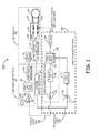
Figure 1 is a simplified schematic diagram of aFOG 100 of one embodiment of the present invention. FOG 100 operates at constant optical power as received at the system photo detector. Constant-power operation is maintained by an intensity servo and light source current control servo driven by an Intensity Digital to Analog Converter and intensity control signal processing circuitry. The construction and operation of conventional FOGs is well known, and as such, will not be discussed in great detail. A representative discussion of FOGs may be found inU.S. Pat. No. 5,465,149 issued Nov. 7, 1995 to Strandjord, et al. , and incorporated by reference herein. - As illustrated in
Figure 1 , FOG 100 comprises alight source 108, a fiber coupler or circulator 110 (referred to herein generically as optical device 110), a multifunctional processing chip referred to herein as an integrated optics chip (IOC) 112, and a fiberoptic coil 114, which are all variously connected byoptical fiber portions fiber coil 114 about a core or spool using a single mode optical fiber wrapped about the axis around which rotation is to be sensed. - The
light source 108 comprises a broadband light source for propagating electromagnetic waves through theFOG 100. In oneembodiment light source 108 is a semiconductor super luminescent diode or a rare earth doped fiber light source which provides electromagnetic waves in the infrared or optical part of the spectrum. In general, thelight source 108 will have a short coherence length for emitted light to reduce the phase shift difference errors between these waves due to Rayleigh and Fresnel scattering at scattering sites in thefiber coil 114. - A
system photo detector 128 detects electromagnetic waves, or light waves, impinging on it from anoptical fiber portion 119, which in turn received the returning combined light beam fromcoupler 110. Thesystem photo detector 128 generates an electrical current in response to the light wave it receives. - In operation, the
light source 108 transmits a broadband light wave to a coupler orcirculator 110 via theoptic fiber 116. A circulator orcoupler 110 transmits light from the light source to theIOC 112 and transmits light returning from theIOC 112 to thesystem photo detector 128. In some embodiments, thecoupler 110 may direct a portion of the light source output to a separate photo detector for reduction of relative intensity noise (RIN), as discussed inFigure 5 below. - The light transmitted to
IOC 112, is further split into two light waves 124, 126 which in one embodiment are phase modulated, such as described inU.S. Pat. No. 5,465,149 , incorporated herein by reference. The two light waves 124, 126 are transmitted to thefiber coil 114, via theoptic fibers fiber coil 114. Similarly, the light wave 126 propagates counterclockwise around the length of thefiber coil 114. After being transmitted from thefiber coil 114, back to theIOC 112 the two returning light waves 124, 126 are combined and then provided to thecoupler 110. The coupler sends the combined light wave tosystem photo detector 128 which feeds the electricalcurrent signal 134 to thesignal processing electronics 104. The rotational rate of thecoil 114 is determined bysignal processing electronics 104 based on optical characteristics of the light received at thephoto detector 128 from interference caused by the Sagnac effect. - In the embodiment of
Figure 1 , constant optical power to thesystem photo detector 128 is maintained by use of a light sourcecurrent servo 102 and intensitycontrol signal processor 105. The intensitycontrol signal processor 105 includes a processor 133 (which may be implemented using technologies such as a Field Programmable Gate Array (FPGA), Application Specific Integrated Circuit (ASIC) and/or a microprocessor that includes digital demodulation and accumulation functions) and intensity D/A converter 136 and anamplifier 138. Combined operation of the light sourcecurrent servo 102 and the intensitycontrol signal processor 105, enables theFOG 100 to maintain operation at an optical power that is sufficient to maintain constant optical power levels atsystem photo detector 128 throughout the life of theFOG 100. Further, an intensity control signal is produced having a DC voltage offset that does not vary with the intensity of the light as received at the system photo detector.Processor 133 further provides an output to IOC D/A converter 139 to provide the bias modulation signal used byIOC 112 to phase modulate the counter-propagating light beams travelling throughcoil 114. - As shown in
Figure 1 , thesignal 134 fromsystem photo detector 128, upon receipt bysignal processing electronics 105, is first amplified (at 130) and then digitized by an A/D converter 132 within thesignal processing electronics 104. The digitized signal is then fed toprocessor 133 for calculation of a digital intensity control word that commands the intensity D/A converter 136. The intensity D/A converter 136 output is amplified (at 138) and fed to the light sourcecurrent servo 102. - In the embodiment shown in
Figure 1 , light sourcecurrent servo 102 comprises a stableanalog reference voltage 140, a comparingamplifier 142, an ultra-low pass filter 144 (having a time constant on the order of tau=1 msec to several hours, for example), and a light sourcecurrent drive 146. - Light source
current servo 102 functions to receive the outputintensity control signal 150 and compares this signal with the stableanalog reference voltage 140 representing a target or nominal optical power on thesystem photo detector 128. Deviations between the actual intensity D/A converter 136 output and the target value are servoed to null. The output of the light sourcecurrent amplifier 142 is heavily low-pass filtered (at 144) to minimize short-term jitter such as quantization noise in optical power. This filtered output, which will slowly vary over the life of theFOG 100 in response to optical loss changes, is fed to light sourcecurrent drive 146 to drivelight source 108, thereby maintaining thesystem photo detector 128 optical power locked at the target or nominal value over life. In the example embodiment, thefilter 144 is an ultra low bandwidth filter. However, it is understood that in alternative embodiments, the filtering can be accomplished by alternate filters known in the art, or in augmentation with, or alternate to a delta sigma approach to fine intensity control/filtering, as described in greater detail below. -
FOG 100 thus provides the ability to slowly and continuously vary the current source in order to maintain constant optical power at thesystem photo detector 128, without introducing step errors or significant quantization noise. The ability to provide constant optical power atsystem photo detector 128 permits the systems to account for loss of light in any of the optical components in theFOG 100. This constancy of optical power at the system photo detector serves to stabilize the signal to noise ratio of the sensor at an intended design value. A second benefit is that stable optical power eliminates scale factor instability in some FOG configurations, such as the so-called open rate-loop FOG, wherein the rotation sensitivity -- or scale factor -- is directly proportional to optical power at the system photo detector. Further, the ability to operateFOG 100 at low optical power (that is, enough to deliver a tolerable optical signal-to-noise ratio atphoto detector 128, yet low enough to minimize nonlinear errors proportional to optical power) reduces bias instability due to these non-linear optical effects. Finally, the light sourcecurrent servo 102 creates a quiet system with low bandwidth, avoiding step errors introduced by sudden adjustments to optical power. -
Figure 2 is a schematic diagram of an alternative embodiment of aFOG 200 having the same configuration as theFOG 100 ofFigure 1 , except that the Intensity Control Signal Processing shown at 105 further includes an optional delta sigma pulse width modulator 210 (also referred to as a delta sigma circuit) in which noise (created by sigma-delta pulse width modulation) is added to the intensity D/A converter signal to reduce quantization noise. In this alternative embodiment, the delta sigmapulse width modulator 210 effectively reduces the quantization of the intensity D/A converter 136 by rapidly dithering (pulse-width modulating) the least significant bits of the intensity D/A digital control word. In this manner, the delta sigma modulator 410 dramatically reduces quantization noise in the intensity servo control loop provided by intensitycontrol signal processor 105 and light sourcecurrent servo 102. Additional details regarding delta sigma pulse width modulation discussed below with respect toFigures 4A and4B are applicable to the delta sigmapulse width modulator 210 ofFigure 2 . -
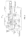
Figure 3 shows that the intensity control servo can be easily and synergistically combined with other functionalities withinFOG 100. For example,Figure 3 shows an embodiment of aFOG 300 in which optical power control is combined with A/D offset signal control. A detailed explanation of A/D offset signal control may be found inU.S. Pat. No. 5,812,263 issued Sep 22, 1998 to Morgan, and incorporated by reference herein. In short, A/D offset signal control is a means of ensuring that the systemphoto detector signal 134, after passing throughamplifier 130, arrives at the A/D converter 132 centered in the finite voltage range of the A/D converter. Such centering not only prevents saturation of the A/D converter 132 (which would result in severe loss of FOG functionality), but also allows maximum gain application atamplifier 130 in order to maximize the rotation signal-to-noise ratio. Such A/D signal centering is important for preventing A/D saturation in rough external environments where events such as radiation or mechanical shock may create relatively rapid step-function changes in optical power and therefore A/D input voltage. Combining optical intensity control with A/D centering allows a FOG to mitigate slowly varying nonlinear optical errors (without introducing new noise) and at the same time keep the A/D centered even through radiation or shock events (which are much too fast for the optical intensity control to mitigate). Further, A/D signal centering minimizes gyroscope performance errors due to finite integral or differential nonlinearity in the A/D converter itself, as will be understood to those skilled in the art. - As
Figure 3 shows, the A/D centering signal 152 and theintensity control signal 150 can be conveniently generated using the single D/A converter 136. The relative bandwidths of theamplifiers D converter 132 input with hundreds of Hz bandwidth, while the light sourcecurrent servo 102 simultaneously may minimize hourly or daily bias drift due to nonlinear optical errors. This combination offers the simultaneous benefits of preventing rapid environmental effects from saturating the A/D converter 132, of minimizing A/D converter 132 nonlinearity error, and servoing out the effects of slowly varying nonlinear optical errors. -
Figure 4A shows one embodiment of aFOG 400 that offers the benefits of both high-bandwidth A/D centering and delta sigma pulse width modulation to minimize quantization noise in optical power control. -
FOG 400 includes a Light sourcecurrent servo 102 andOptical Circuit 101 such as described inFigures 1-3 .FOG 400 further includessignal processing electronics 404 that includes afirst amplifier 430, an A/D converter 432, and aprocessor 434 which operate as described with respect toamplifier 130, A/D converter 132 andprocessor 133 described above. UnlikeFOG 100, in this embodiment the intensitycontrol signal processor 405 includes two separate D/A converters: one to maintain the A/D centering (shown at 412) and a second (shown at 414) to null slow optical power drifts that would otherwise create nonlinear optical errors. - The intensity control D/
A converter 414 is independent from the offset signal D/A converter 412 and relies on thesignal 406 fed digitally into the delta sigmapulse width modulator 410.Signal 406 is provided to the delta sigma pulse width modulator 410 (also referred to as a delta sigma circuit) and eventually feeds the output signal 411 to the intensity D/A converter 414, much like the intensity D/A converter DAC 136 ofFigure 3 , to convert thesignal 406 into the analog domain to provide theintensity control signal 150 to light sourcecurrent servo 102. - Meanwhile, the offset signal D/
A converter 412 relies on thesignal 406 to produce A/D centering signal 452, which is amplified (at 415), summed with the systemphoto detector signal 134 and provided back throughamplifier 430 to drive thesignal processing electronics 404. As mentioned above, A/D offset signal control is a means of ensuring that the systemphoto detector signal 134, after passing throughamplifier 430, arrives at the A/D converter 432 centered in the finite voltage range of the A/D converter. Such A/D signal centering prevents saturation of A/D converter 432 (even under dynamic vibration, shock, and radiation conditions) and also minimizesFOG 400 performance errors due to finite integral or differential nonlinearity in the A/D converter itself, as will be understood to those skilled in the art. - The example embodiment of
Figure 4A has various advantages. First, by utilizing theindependent intensity DAC 414, the light sourcecurrent servo 102 is shielded from large changes in external environments that could potentially affect theoutput 452 of the offset signal D/A loop if assumed present in circuit. As such, the outer loop created by the light sourcecurrent servo 102 can operate with lower-cost components and less filtering capability, yet still preventing potential noise from theloop 452 affecting functionality. Although in this case, two separate D/A converters are shown for clarity, (i.e., one for the offset control function and another for the intensity control with delta-sigma modulation) in some embodiments it is possible to perform both functions with a single D/A converter. -
Figure 4B is a schematic diagram of an embodiment of delta sigmapulse width modulator 410. The delta sigmapulse width modulator 410 receives signal 406 which is a high precision digital representation of optical power and uses balanced, high frequency pulse width modulation of intensity D/A converter 414 (at a frequency well above gyro noise sensitivities) to produce mean analog values having greater resolution than D/A converter 414 is capable of without this dithering. The output, as expressed by intensity D/A converter 414, is then provided to light sourcecurrent servo 102 where it is compared against the highprecision voltage reference 140. The initial value of light source current provided by the light sourcecurrent servo 102 may be programmable by a user or an alternative functional circuit, and determined at the time of operation or at some time prior to operation. The delta sigmapulse width modulator 410 uses signal 406 and servos the mean output via an integrated feedback loop (comprising asummer 416,integrator 418 and Pulse Width Quantizer 419) and theultralow bandwidth servo 102 to remove integrated error. That is, the finite quantization steps of thesignal 406 are averaged out by dithering thesignal 406 low order bits and then integrating inamplifier 418 with the loop bandwidth filters. - The delta sigma approach of
Figures 4A and4B also has a variety of advantages. First, much like the embodiment inFigure 3 , the delta sigma circuitry ofmodulator 410 is independent of the offset signal D/A loop withinsignal processing electronics 404 and therefore is not heavily affected by noise created within that comparatively high-bandwidth loop. Furthermore, the delta sigma approach permits sufficiently small pump current step changes with sufficiently filtered noise components to operateintensity control signal 150. Thus, the delta sigma approach ofFigures 4A and4B allows the light sourcecurrent servo 102 to deliver high current control performance even using low-cost modest-performing, components. - In yet another embodiment illustrated in
Figure 5 , the control of optical power achieved by sourcecurrent servo 102 can be combined with still other functionalities withinFOG 100. For example,Figure 5 shows an embodiment (generally at 500) in which the optical power control demonstrated inFigure 3 is combined with additional circuitry withinSignal Processing Electronics 104 to reduce the effects of relative intensity noise (RIN). RIN is often a dominant source of rotation rate measurement noise in FOGs, as is well known to those skilled in the art.U.S. Pats. No. 5,469,257 issued Nov 21, 1995 to Blake et al andU.S. Pat. No. 6,765,678 issued Jul. 20, 2004 , both incorporated by reference herein, describe methods to reduce the effect of RIN on FOG noise.Figure 5 conveys an embodiment in which a second photo detector 532 (called RIN photo detector 532) coupled to coupler/circulator 110 senses the relative intensity noise generated in thelight source 108. This noise is common mode with noise on thesystem photo detector 128, and therefore subtraction of the two photo detector signals results in a system photo detector signal with much of the RIN eliminated. This subtraction approach relies on accurate knowledge and/or normalization of the DC optical power on both photo detectors. In the embodiment ofFigure 5 ,Signal Processing Electronics 104 further comprises aRIN amplifier 510, a RIN A/D converter 512 and aRIN demodulation block 514.RIN amplifier 510 receives the output fromRIN photo detector 532 and the RIN detector optical power can be determined from the output of theRIN demodulation block 514. A difference (taken at 518) between the output fromRIN photo detector 532 and the output from a rate demodulator 516 (which is generated from system photo detector signal 134) is provided toprocessor 133. The system detector power can then be determined from the intensity D/A control word provided byprocessor 133 to intensity D/A converter 136. - Although the embodiments discussed above have described utilizing the system photo detector to stabilize optical power as measured from light exiting the optical coil, other embodiments within the scope of the present invention may alternately stabilize optical power entering the coil in order to, for example, correct for nonlinear optical effect near the entrance to the coil. One of ordinary skill in the art upon studying this specification would appreciate that this could be achieved by utilizing a photo detector (via a coupler, for example) that monitors optical power of the light beam traveling towards the coil, prior to the splitting of the light beam. A RIN photo detector is one example of where this optical power could be measured.
-
Figure 6 illustrates one detailed embodiment(at 600) where optical power control ofoptical circuit 101 by light sourcecurrent servo 102 is combined with RIN subtraction and another beneficial functionality, namely digital intensity normalization, to suppress the effects of rapid intensity modulations from vibrations up to kHz or even tens of kHz frequencies. Digital intensity normalization thus happens at very high bandwidth - much higher than optical intensity control, and even higher than A/D centering. Hence by combining optical intensity control, A/D centering, and digital intensity normalization, the embodiment ofFigure 6 covers a wider-than-ever range of frequencies/timescales over which error can be eliminated. - Within
signal processing electronics 604, digital intensity normalization is implemented by anormalization circuit 610 such as that seen inFigure 6 . The concept of digital normalization is described inU.S. Pub. No. 2008/0,079,946 A1 published on April 3, 2008 to Greening and incorporated by reference herein. In the embodiment ofFigure 6 , both theRate demodulation circuit 616 andRIN Demod 614 output signals are normalized at 610 before subtraction at 618. This normalization ensures that slow adjustments of optical power by the light sourcecurrent servo 102 do not reduce the efficacy of RIN subtraction. Further, it may be understood that by combining low-bandwidth optical power control with higher-bandwidth A/D offset centering (shown generally at 620) and ultra-high bandwidth intensity normalization, it is possible to suppress gyroscope error mechanisms over a dynamic range from sub-Hz to tens of kHz. - Note that in alternative embodiments, the
rate demodulation circuit 616 can be a synchronous or an asynchronous design, depending on the needs of the system. The details of synchronous and asynchronous demodulation designs are discussed inU.S. Pat. No. 7,333,209 issued May 10, 2007 to Greening, et al. , and incorporated by reference herein. The optical power control provided by embodiment of the present invention is compatible with both synchronous and asynchronous demodulation. In one embodiment, the relative intensity noise-reduced rotation rate signal is used to generate an error suppression modulation signal that drives modulation of the light travelling through the optical path. Further, in one embodiment a digital-to-analog converter loop ofelectronics 604 is coupled to receive theelectrical signal 134 from thesystem photo detector 128 and output anintensity control signal 150 having a DC voltage offset that does not vary with the intensity of the light as received at thesystem photo detector 128. As illustrated inFigure 6 ,signal processing electronics 604 outputs a digital control signal that is converted to analog (at 622) and amplified (at 624) to generate the bias modulation signal that drives modulation of the light beams inIOC 112. -
Figure 7 is a flow diagram of an embodiment of a method of one embodiment of the present invention. The method begins at 710 with determining an intensity of light within an optic path of a fiber optic gyroscope as measured at a system photo detector, wherein light within the optic path is generated by a light source. The method proceeds to 720 with controlling an electrical current output of a light source current drive that powers the light source with a light source current servo by comparing an analog signal derived from the intensity of light within the optic path, for example at the system photo detector, against a stable analog voltage reference. - The method proceeds to 730 with applying a filter to adjustments of the light source current drive that removes quantization noise from the electric current output. In one embodiment, applying a filter to adjustments of the light source current drive comprises applying an ultra low bandwidth filter to a signal that controls the light source current drive. By utilizing a light source current servo having a long time constant (on the order of seconds to hours, for example), the light source current is slowly and smoothly adjusted without abrupt steps, glitches or hysteresis. In another embodiment, applying a filter comprises processing a digital loop output signal with a delta sigma integrated feedback loop that integrates out a noise spectrum from the digital loop output signal. In other embodiments, other forms of filtering may be applied, or combined, as would be appreciated by one of ordinary skill in the art upon reading this specification.
- In one embodiment of the method presented in
Figure 7 , the light source current servo functions to receive an output signal from an intensity D/A converter within a set of signal processing electronics, and filters the signal to achieve a light source current that will drive the gyroscope's light source with no significant quantization noise. This filtered output, which will slowly vary over the life of the FOG, is fed to the light source current drive to drive the light source. Further, by signal processing electronics which includes an A/D centering control loop and a digital intensity normalization circuit, the FOG gains insensitivity to external forces. - This description is presented for purposes of illustration, and is not intended to be exhaustive or limited to the embodiments disclosed. Variations and modifications may occur, which fall within the scope of the following claims. For example, the embodiments described above relate to a FOG, but it is understood that any variation or species of FOG can utilize the described invention. Furthermore, some of the components described below may be implemented using either digital or analog circuitry, or a combination of both, and, where appropriate, realized through software executing on a suitable processing circuitry and machine-readable storage mediums.
- Several means are available to implement the systems and methods of the current invention as discussed in this specification. These means include, but are not limited to, digital computer systems, microprocessors, application-specific integrated circuits (ASIC), general purpose computers, programmable controllers and field programmable gate arrays (FPGAs), all of which may be generically referred to herein as "processors". For example, in one embodiment, signal processing may be incorporated by an FPGA or an ASIC, or alternatively by an embedded or discrete processor. Therefore other embodiments of the present invention are program instructions resident on computer readable media which when implemented by such means enable them to implement embodiments of the present invention. Computer readable media include any form of a physical computer memory device. Examples of such a physical computer memory device include, but is not limited to, punch cards, magnetic disks or tapes, optical data storage system, flash read only memory (ROM), non-volatile ROM, programmable ROM (PROM), erasable-programmable ROM (E-PROM), random access memory (RAM), or any other form of permanent, semi-permanent, or temporary memory storage system or device. Program instructions include, but are not limited to computer-executable instructions executed by computer system processors and hardware description languages such as Very High Speed Integrated Circuit (VHSIC) Hardware Description Language (VHDL).
- Although specific embodiments have been illustrated and described herein, it will be appreciated by those of ordinary skill in the art that any arrangement, which is calculated to achieve the same purpose, may be substituted for the specific embodiment shown. This application is intended to cover any adaptations or variations of the present invention. Therefore, it is manifestly intended that this invention be limited only by the claims and the equivalents thereof.
Claims (10)
- A fiber optic gyroscope 100, the fiber optic gyroscope 100 comprising:a light source current servo 102 coupled to a gyroscope light source 108 that transmits light through an optic path, wherein the light source current servo 102 controls intensity of the light through the optic path via a light source current drive 146 that supplies current to power the gyroscope light source 108; andan intensity control signal processor 105 coupled to the optic path via a photo detector 128, wherein the intensity control signal processor 105 outputs an intensity control signal to the light source current servo 102, wherein the intensity control signal is a function of intensity of the light as received at the photo detector 128;wherein the light source current servo 102 compares the intensity control signal against a stable analog voltage reference to adjust the light source current drive 146 and drive optical power at the photo detector 128 towards a constant optical power level.
- The fiber optic gyroscope of claim 1, wherein the intensity control signal processor 105 further comprises: an intensity digital-to-analog converter 136 coupled to a processor 133, wherein the intensity digital-to-analog converter136 receives a digital intensity control word from the processor 133 that provides a digital representation of optical power received at the photo detector 128.
- The fiber optic gyroscope of claim 2, wherein the intensity digital-to-analog converter 136 outputs an analog intensity signal representing intensity of the light as received at the photo detector 128.
- The fiber optic gyroscope of claim 2, wherein the light source current servo 102 applies a filter to adjustments of the light source currenty drive 146 to remove quantization noise.
- The fiber optic gyroscope of claim 4, wherein the light source current servo 102 loop further comprises:a delta sigma circuit 210 that receives the digital intensity control word, wherein the delta sigma circuit's output signal is a pulse width modulated (PWM) intensity control signal;an intensity digital-to-analog converter 136 that converts the output of the delta sigma circuit into analog.
- The fiber optic gyroscope of claim 5, wherein the delta sigma circuit 210 comprises:an integrated feedback loop (416, 418, 419) which integrates out a noise spectrum from the digital loop output signal.
- The fiber optic gyroscope of claim 1, wherein the intensity control signal processor 105 further comprises:an intensity digital-to-analog converter 136 coupled to receive a digital intensity control word and output a signal representing intensity of the light as received at the photo detector 128;a digital intensity normalization circuit 610 coupled to the intensity digital-to-analog converter;a rate demodulation circuit 616 coupled to the intensity digital-to-analog converter; anda relative intensity noise demodulation circuit 614 coupled to the intensity digital-to-analog converter;an analog-to-digital offset center control loop 620 coupled to the intensity digital-to-analog converter;a relative intensity noise subtraction circuit 618 coupled to the digital intensity normalization circuit;wherein an output of the rate demodulation circuit is digitally normalized by a digital measure of optical intensity to produce a normalized rate;
wherein an output of the relative intensity noise demodulation circuit is digitally normalized by a digital measure of optical intensity;
wherein the normalized rate and an output of the relative intensity noise demodulation circuit are combined to produce a relative intensity noise -reduced measure of rotation rate. - The fiber optic gyroscope of claim 7, wherein the relative intensity noise-reduced rotation rate signal is used to generate an error suppression modulation signal that drives modulation of the light travelling through the optical path.
- The fiber optic gyroscope of claim 7, further comprising a relative intensity noise photo detector 128 coupled to the optic path, the relative intensity noise subtraction circuit 618 further coupled to the relative intensity noise photo detector 128.
- The fiber optic gyroscope of claim 1, wherein the optic path further comprises:a fiber coil 114 having a first end and a second end;an integrated optical circuit 112 coupled to the first end and the second end of the fiber coil 114; andan optical device 110 that directs the light from the gyroscope light source 108 to the integrated optical circuit;wherein the integrated optical circuit 112 splits the light from the light source 108 into a first light beam directed to the first end of the fiber coil 114 and a second light beam directed to the second end of the fiber coil 114;
wherein the optical device 110 further directs a returning light beam from the integrated optical circuit to the photo detector 128.
Applications Claiming Priority (1)
| Application Number | Priority Date | Filing Date | Title |
|---|---|---|---|
| US12/943,352 US8213018B2 (en) | 2010-11-10 | 2010-11-10 | Constant optical power sensor using a light source current servo combined with digital demodulation intensity suppression for radiation and vibration insensitivity in a fiber optic gyroscope |
Publications (2)
| Publication Number | Publication Date |
|---|---|
| EP2453206A1 true EP2453206A1 (en) | 2012-05-16 |
| EP2453206B1 EP2453206B1 (en) | 2014-02-26 |
Family
ID=44993502
Family Applications (1)
| Application Number | Title | Priority Date | Filing Date |
|---|---|---|---|
| EP11188460.7A Active EP2453206B1 (en) | 2010-11-10 | 2011-11-09 | Fiber optic gyroscope with constant optical power using a light source current servo combined with digital demodulation intensity suppression for radiation and vibration insensitivity |
Country Status (3)
| Country | Link |
|---|---|
| US (1) | US8213018B2 (en) |
| EP (1) | EP2453206B1 (en) |
| JP (1) | JP2012103251A (en) |
Cited By (2)
| Publication number | Priority date | Publication date | Assignee | Title |
|---|---|---|---|---|
| CN102759366A (en) * | 2012-07-11 | 2012-10-31 | 北京理工大学 | Detection device of optical fiber gyroscope optical module |
| EP2899504B1 (en) * | 2014-01-22 | 2023-06-07 | Northrop Grumman Systems Corporation | Adaptive inertial measurement system and method |
Families Citing this family (12)
| Publication number | Priority date | Publication date | Assignee | Title |
|---|---|---|---|---|
| CN102818565B (en) * | 2012-08-09 | 2014-12-10 | 浙江大学 | Suppression method of relative intensity noise of light source of fiber-optic gyroscope |
| US9568317B2 (en) * | 2013-01-31 | 2017-02-14 | Honeywell International Inc. | Fiber optic gyroscope mixed signal application specific integrated circuit |
| CN106885565B (en) * | 2017-02-14 | 2020-02-07 | 北京航空航天大学 | Suppression method for adding zero offset to output signal of interferometric fiber-optic gyroscope based on median filtering |
| US10429187B1 (en) | 2018-09-04 | 2019-10-01 | Honeywell International Inc. | Apparatus and method for optical power control |
| CN109141478A (en) * | 2018-10-11 | 2019-01-04 | 湖南航天机电设备与特种材料研究所 | Optical fibre gyro feedback loop nonlinearity test method |
| CN110986914A (en) * | 2019-12-13 | 2020-04-10 | 西安航天精密机电研究所 | Method and system for rapidly stabilizing optical power of light source for fiber-optic gyroscope |
| CN113252021B (en) * | 2021-07-05 | 2021-11-02 | 西安中科华芯测控有限公司 | A pre-flight self-check method and self-check system of fiber optic gyro with high coverage |
| CN115031759B (en) * | 2022-02-25 | 2024-07-26 | 长光卫星技术股份有限公司 | On-orbit fiber optic gyroscope noise acquisition method based on equivalent noise bandwidth method, readable storage medium and electronic equipment |
| CN115420272B (en) * | 2022-08-24 | 2024-04-26 | 北京航空航天大学 | Method for realizing adaptive suppression of relative intensity noise of optical fiber gyro light source |
| CN115900679B (en) * | 2023-03-08 | 2023-05-12 | 中国船舶集团有限公司第七〇七研究所 | Method for improving signal-to-noise ratio of integrated optical gyroscope |
| US12535320B2 (en) * | 2023-05-11 | 2026-01-27 | Honeywell International Inc. | Resonant optical gyroscope with a broadband light source and RIN reduction techniques |
| CN118999514B (en) * | 2024-08-14 | 2025-09-16 | 浙江大学 | A binary modulation deep optical path power compensation system and method for fiber optic gyroscope |
Citations (9)
| Publication number | Priority date | Publication date | Assignee | Title |
|---|---|---|---|---|
| US5208652A (en) * | 1990-04-26 | 1993-05-04 | Hitachi, Ltd. | An improved optical branching/coupling unit for an optical fiber gyroscope, and navigation system employing the same |
| US5444533A (en) * | 1992-09-02 | 1995-08-22 | Sumitomo Electric Industries, Ltd. | Fiber-optic gyroscope obtaining a signal from a perturbed light source |
| US5465149A (en) | 1994-03-10 | 1995-11-07 | Honeywell Inc. | Lightwave phase control for reduction of resonator fiber optic gyroscope Kerr effect error |
| US5469257A (en) | 1993-11-24 | 1995-11-21 | Honeywell Inc. | Fiber optic gyroscope output noise reducer |
| US5812263A (en) | 1996-12-20 | 1998-09-22 | Morgan; Avery A. | Accuracy of a fiber optic gyro |
| US6765678B2 (en) | 2002-01-08 | 2004-07-20 | Honeywell International Inc. | Relative intensity noise controller with maximum gain at frequencies at or above the bias modulation frequency or with second order feedback for fiber light sources |
| US20040233455A1 (en) * | 2001-08-03 | 2004-11-25 | Manfred Keller | Increasing of the long-term operational reliability of a fiber optic interferometer by protecting the light source |
| US7333209B2 (en) | 2005-11-09 | 2008-02-19 | Honeywell International, Inc. | Fiber optic gyroscope asynchronous demodulation |
| US20080079946A1 (en) | 2006-09-29 | 2008-04-03 | Honeywell International, Inc. | Digital intensity suppression for vibration and radiation insensitivity in a fiber optic gyroscope |
Family Cites Families (34)
| Publication number | Priority date | Publication date | Assignee | Title |
|---|---|---|---|---|
| JPS5913910A (en) * | 1982-07-15 | 1984-01-24 | Nec Corp | Optical fiber gyro |
| FR2612300B1 (en) | 1987-03-13 | 1989-05-26 | Thomson Csf | OPTICAL SIGNAL REJECTION FILTER AND APPLICATIONS TO RING INTERFEROMETERS |
| FR2616538B1 (en) | 1987-06-11 | 1989-09-01 | Alsthom | SAGNAC-TYPE FIBER OPTIC INTERFEROMETRIC SYSTEM |
| JPH0652173B2 (en) * | 1989-03-23 | 1994-07-06 | 日本航空電子工業株式会社 | Hikari Watanabe |
| US5080489A (en) | 1989-03-29 | 1992-01-14 | Kubota, Ltd. | Fiber optic gyroscope for detecting angular velocity of rotation using equivalent time sampling |
| FR2654827B1 (en) * | 1989-11-17 | 1992-03-20 | Photonetics | FIBER OPTIC MEASUREMENT DEVICE, GYROMETER, NAVIGATION AND STABILIZATION UNIT. |
| US5024535A (en) | 1989-12-20 | 1991-06-18 | United Technologies Corporation | Semiconductor light source temperature measurement |
| US5264914A (en) | 1990-03-02 | 1993-11-23 | Hitachi Ltd | Interference sensor and method utilizing extracted alliasing frequency components |
| US5136600A (en) | 1990-09-18 | 1992-08-04 | Litton Systems Inc. | Stabilization apparatus and method for an sfs |
| US5196904A (en) | 1990-12-31 | 1993-03-23 | Honeywell Inc. | Fiber optic gyroscope bias modulation amplitude determination |
| JPH06201388A (en) * | 1992-12-28 | 1994-07-19 | Sumitomo Electric Ind Ltd | Gyro device |
| EP0618653B1 (en) | 1993-03-30 | 1997-07-16 | Nec Corporation | Frequency stabilization method of semiconductor laser and frequency-stabilized light source |
| US5410515A (en) | 1993-04-29 | 1995-04-25 | Honeywell Inc. | Rapid turn-on source for fiber optic gyroscope |
| US5329349A (en) | 1993-05-10 | 1994-07-12 | Litton Systems, Inc. | Method for tuning fiber optic sensor coils |
| AU6339594A (en) | 1993-06-09 | 1994-12-15 | Alcatel N.V. | Synchronized clock |
| US5489981A (en) * | 1994-05-27 | 1996-02-06 | Honeywell Inc. | Microprocessor controlled anglaser gyropower control system |
| JP2849734B2 (en) * | 1994-06-22 | 1999-01-27 | 日本航空電子工業株式会社 | Fiber optic gyro |
| US5530545A (en) | 1994-07-29 | 1996-06-25 | Litton Systems, Inc. | Method for reducing random walk in fiber optic gyroscopes |
| US6215809B1 (en) | 1996-03-25 | 2001-04-10 | Sdl, Inc. | Stabilization of laser sources with closely-coupled optical reflectors using an internal dither circuit |
| US5812572A (en) | 1996-07-01 | 1998-09-22 | Pacific Fiberoptics, Inc. | Intelligent fiberoptic transmitters and methods of operating and manufacturing the same |
| US5898496A (en) | 1997-02-14 | 1999-04-27 | Allied Signal Inc | Optical signal noise reduction for fiber optic gyroscopses |
| US5923424A (en) | 1997-06-19 | 1999-07-13 | Honeywell Inc. | Fiber optic gyroscope vibration error compensator |
| US5926275A (en) * | 1997-06-19 | 1999-07-20 | Honeywell Inc. | Vibration error reduction servo for a fiber optic gyroscope |
| US6028668A (en) | 1998-02-04 | 2000-02-22 | Rockwell Collins, Inc. | Fiber optic gyroscope having improved readout and modulation index control |
| US6359918B1 (en) | 1998-06-30 | 2002-03-19 | Honeywell International Inc. | Light source control device |
| JP2000146597A (en) * | 1998-11-06 | 2000-05-26 | Tokimec Inc | Optical fiber gyro |
| US6657729B2 (en) | 2000-03-27 | 2003-12-02 | Honeywell International Inc. | Dithering system and method for a laser diode light source for an optical gyroscope |
| JP2002230905A (en) * | 2001-01-29 | 2002-08-16 | Niigata Seimitsu Kk | Audio reproduction apparatus and method |
| US6744966B2 (en) | 2001-11-14 | 2004-06-01 | Honeywell International, Inc. | Radiation insensitive fiber light source for interferometric fiber optic gyroscopes (IFOGS) |
| US7167250B2 (en) | 2002-04-30 | 2007-01-23 | Honeywell International, Inc. | System and method for reducing fiber optic gyroscope color noise |
| JP2004304494A (en) * | 2003-03-31 | 2004-10-28 | Fuji Electric Holdings Co Ltd | A / D converter of ΔΣ modulation method and control device using the same |
| US7038783B2 (en) | 2003-05-23 | 2006-05-02 | Honeywell International Inc. | Eigen frequency detector for Sagnac interferometers |
| US7388670B2 (en) * | 2005-12-05 | 2008-06-17 | Honeywell International Inc. | LASER gyro readout signal stabilization in high vibration environments |
| JP2010169532A (en) * | 2009-01-22 | 2010-08-05 | Panasonic Corp | Drive circuit and physical quantity sensor apparatus |
-
2010
- 2010-11-10 US US12/943,352 patent/US8213018B2/en active Active
-
2011
- 2011-11-09 JP JP2011245607A patent/JP2012103251A/en not_active Ceased
- 2011-11-09 EP EP11188460.7A patent/EP2453206B1/en active Active
Patent Citations (9)
| Publication number | Priority date | Publication date | Assignee | Title |
|---|---|---|---|---|
| US5208652A (en) * | 1990-04-26 | 1993-05-04 | Hitachi, Ltd. | An improved optical branching/coupling unit for an optical fiber gyroscope, and navigation system employing the same |
| US5444533A (en) * | 1992-09-02 | 1995-08-22 | Sumitomo Electric Industries, Ltd. | Fiber-optic gyroscope obtaining a signal from a perturbed light source |
| US5469257A (en) | 1993-11-24 | 1995-11-21 | Honeywell Inc. | Fiber optic gyroscope output noise reducer |
| US5465149A (en) | 1994-03-10 | 1995-11-07 | Honeywell Inc. | Lightwave phase control for reduction of resonator fiber optic gyroscope Kerr effect error |
| US5812263A (en) | 1996-12-20 | 1998-09-22 | Morgan; Avery A. | Accuracy of a fiber optic gyro |
| US20040233455A1 (en) * | 2001-08-03 | 2004-11-25 | Manfred Keller | Increasing of the long-term operational reliability of a fiber optic interferometer by protecting the light source |
| US6765678B2 (en) | 2002-01-08 | 2004-07-20 | Honeywell International Inc. | Relative intensity noise controller with maximum gain at frequencies at or above the bias modulation frequency or with second order feedback for fiber light sources |
| US7333209B2 (en) | 2005-11-09 | 2008-02-19 | Honeywell International, Inc. | Fiber optic gyroscope asynchronous demodulation |
| US20080079946A1 (en) | 2006-09-29 | 2008-04-03 | Honeywell International, Inc. | Digital intensity suppression for vibration and radiation insensitivity in a fiber optic gyroscope |
Cited By (3)
| Publication number | Priority date | Publication date | Assignee | Title |
|---|---|---|---|---|
| CN102759366A (en) * | 2012-07-11 | 2012-10-31 | 北京理工大学 | Detection device of optical fiber gyroscope optical module |
| CN102759366B (en) * | 2012-07-11 | 2014-11-26 | 北京理工大学 | Detection device of optical fiber gyroscope optical module |
| EP2899504B1 (en) * | 2014-01-22 | 2023-06-07 | Northrop Grumman Systems Corporation | Adaptive inertial measurement system and method |
Also Published As
| Publication number | Publication date |
|---|---|
| JP2012103251A (en) | 2012-05-31 |
| US20120113432A1 (en) | 2012-05-10 |
| US8213018B2 (en) | 2012-07-03 |
| EP2453206B1 (en) | 2014-02-26 |
Similar Documents
| Publication | Publication Date | Title |
|---|---|---|
| US8213018B2 (en) | Constant optical power sensor using a light source current servo combined with digital demodulation intensity suppression for radiation and vibration insensitivity in a fiber optic gyroscope | |
| US6744519B2 (en) | Methods and apparatus for fiber optic gyroscope dead band error suppression modulation | |
| EP1144950B1 (en) | System for suppression of relative intensity noise in a fiber optic gyroscope | |
| EP1906145A2 (en) | Digital intensity suppression for reducing vibration and radiation sensitivity in a fiber gyroscope | |
| EP1718929B1 (en) | System and method for reducing fiber optic gyroscope color noise | |
| US9557174B2 (en) | Fiber optic gyroscope dead band error suppression | |
| US6583882B2 (en) | Apparatus and method using digitally controlled integration for signal detection with improved noise characteristics | |
| US5953122A (en) | Method and apparatus for increasing the stability of a fiber optic gyroscope by controlling the phase and amplitude of the source modulating current | |
| US5196904A (en) | Fiber optic gyroscope bias modulation amplitude determination | |
| EP4538640A1 (en) | Systems and methods for effective relative intensity noise subtraction for a broadband resonator optical gyroscope | |
| US7324206B2 (en) | Method for determination/compensation of bias errors/random walk errors induced by the light source in fiber-optic Sagnac interferometers | |
| US5283626A (en) | Fiber optic gyroscope bias modulation amplitude determination with reset means | |
| EP0492580B1 (en) | Fiber optic gyro | |
| JP2557658B2 (en) | Optical interference gyro | |
| JP2840985B2 (en) | Fiber optic gyroscope | |
| US20040174528A1 (en) | Schemes for computing performance parameters of fiber optic gyroscopes | |
| Nuño et al. | Fiber optic gyroscope assisted by Raman amplification | |
| JPH0625669B2 (en) | Optical interference gyro |
Legal Events
| Date | Code | Title | Description |
|---|---|---|---|
| PUAI | Public reference made under article 153(3) epc to a published international application that has entered the european phase |
Free format text: ORIGINAL CODE: 0009012 |
|
| 17P | Request for examination filed |
Effective date: 20111109 |
|
| AK | Designated contracting states |
Kind code of ref document: A1 Designated state(s): AL AT BE BG CH CY CZ DE DK EE ES FI FR GB GR HR HU IE IS IT LI LT LU LV MC MK MT NL NO PL PT RO RS SE SI SK SM TR |
|
| AX | Request for extension of the european patent |
Extension state: BA ME |
|
| RIC1 | Information provided on ipc code assigned before grant |
Ipc: G01C 19/72 20060101AFI20130510BHEP |
|
| GRAP | Despatch of communication of intention to grant a patent |
Free format text: ORIGINAL CODE: EPIDOSNIGR1 |
|
| INTG | Intention to grant announced |
Effective date: 20130923 |
|
| GRAP | Despatch of communication of intention to grant a patent |
Free format text: ORIGINAL CODE: EPIDOSNIGR1 |
|
| GRAS | Grant fee paid |
Free format text: ORIGINAL CODE: EPIDOSNIGR3 |
|
| INTG | Intention to grant announced |
Effective date: 20140106 |
|
| GRAA | (expected) grant |
Free format text: ORIGINAL CODE: 0009210 |
|
| AK | Designated contracting states |
Kind code of ref document: B1 Designated state(s): AL AT BE BG CH CY CZ DE DK EE ES FI FR GB GR HR HU IE IS IT LI LT LU LV MC MK MT NL NO PL PT RO RS SE SI SK SM TR |
|
| REG | Reference to a national code |
Ref country code: GB Ref legal event code: FG4D |
|
| REG | Reference to a national code |
Ref country code: CH Ref legal event code: EP |
|
| REG | Reference to a national code |
Ref country code: AT Ref legal event code: REF Ref document number: 653861 Country of ref document: AT Kind code of ref document: T Effective date: 20140315 |
|
| REG | Reference to a national code |
Ref country code: IE Ref legal event code: FG4D |
|
| REG | Reference to a national code |
Ref country code: DE Ref legal event code: R096 Ref document number: 602011005050 Country of ref document: DE Effective date: 20140410 |
|
| REG | Reference to a national code |
Ref country code: NL Ref legal event code: VDEP Effective date: 20140226 |
|
| REG | Reference to a national code |
Ref country code: AT Ref legal event code: MK05 Ref document number: 653861 Country of ref document: AT Kind code of ref document: T Effective date: 20140226 |
|
| REG | Reference to a national code |
Ref country code: LT Ref legal event code: MG4D |
|
| PG25 | Lapsed in a contracting state [announced via postgrant information from national office to epo] |
Ref country code: IS Free format text: LAPSE BECAUSE OF FAILURE TO SUBMIT A TRANSLATION OF THE DESCRIPTION OR TO PAY THE FEE WITHIN THE PRESCRIBED TIME-LIMIT Effective date: 20140626 Ref country code: NO Free format text: LAPSE BECAUSE OF FAILURE TO SUBMIT A TRANSLATION OF THE DESCRIPTION OR TO PAY THE FEE WITHIN THE PRESCRIBED TIME-LIMIT Effective date: 20140526 Ref country code: LT Free format text: LAPSE BECAUSE OF FAILURE TO SUBMIT A TRANSLATION OF THE DESCRIPTION OR TO PAY THE FEE WITHIN THE PRESCRIBED TIME-LIMIT Effective date: 20140226 |
|
| PG25 | Lapsed in a contracting state [announced via postgrant information from national office to epo] |
Ref country code: SE Free format text: LAPSE BECAUSE OF FAILURE TO SUBMIT A TRANSLATION OF THE DESCRIPTION OR TO PAY THE FEE WITHIN THE PRESCRIBED TIME-LIMIT Effective date: 20140226 Ref country code: AT Free format text: LAPSE BECAUSE OF FAILURE TO SUBMIT A TRANSLATION OF THE DESCRIPTION OR TO PAY THE FEE WITHIN THE PRESCRIBED TIME-LIMIT Effective date: 20140226 Ref country code: CY Free format text: LAPSE BECAUSE OF FAILURE TO SUBMIT A TRANSLATION OF THE DESCRIPTION OR TO PAY THE FEE WITHIN THE PRESCRIBED TIME-LIMIT Effective date: 20140226 Ref country code: FI Free format text: LAPSE BECAUSE OF FAILURE TO SUBMIT A TRANSLATION OF THE DESCRIPTION OR TO PAY THE FEE WITHIN THE PRESCRIBED TIME-LIMIT Effective date: 20140226 Ref country code: PT Free format text: LAPSE BECAUSE OF FAILURE TO SUBMIT A TRANSLATION OF THE DESCRIPTION OR TO PAY THE FEE WITHIN THE PRESCRIBED TIME-LIMIT Effective date: 20140626 Ref country code: NL Free format text: LAPSE BECAUSE OF FAILURE TO SUBMIT A TRANSLATION OF THE DESCRIPTION OR TO PAY THE FEE WITHIN THE PRESCRIBED TIME-LIMIT Effective date: 20140226 |
|
| PG25 | Lapsed in a contracting state [announced via postgrant information from national office to epo] |
Ref country code: LV Free format text: LAPSE BECAUSE OF FAILURE TO SUBMIT A TRANSLATION OF THE DESCRIPTION OR TO PAY THE FEE WITHIN THE PRESCRIBED TIME-LIMIT Effective date: 20140226 Ref country code: HR Free format text: LAPSE BECAUSE OF FAILURE TO SUBMIT A TRANSLATION OF THE DESCRIPTION OR TO PAY THE FEE WITHIN THE PRESCRIBED TIME-LIMIT Effective date: 20140226 Ref country code: BE Free format text: LAPSE BECAUSE OF FAILURE TO SUBMIT A TRANSLATION OF THE DESCRIPTION OR TO PAY THE FEE WITHIN THE PRESCRIBED TIME-LIMIT Effective date: 20140226 |
|
| PG25 | Lapsed in a contracting state [announced via postgrant information from national office to epo] |
Ref country code: DK Free format text: LAPSE BECAUSE OF FAILURE TO SUBMIT A TRANSLATION OF THE DESCRIPTION OR TO PAY THE FEE WITHIN THE PRESCRIBED TIME-LIMIT Effective date: 20140226 Ref country code: CZ Free format text: LAPSE BECAUSE OF FAILURE TO SUBMIT A TRANSLATION OF THE DESCRIPTION OR TO PAY THE FEE WITHIN THE PRESCRIBED TIME-LIMIT Effective date: 20140226 Ref country code: RO Free format text: LAPSE BECAUSE OF FAILURE TO SUBMIT A TRANSLATION OF THE DESCRIPTION OR TO PAY THE FEE WITHIN THE PRESCRIBED TIME-LIMIT Effective date: 20140226 Ref country code: EE Free format text: LAPSE BECAUSE OF FAILURE TO SUBMIT A TRANSLATION OF THE DESCRIPTION OR TO PAY THE FEE WITHIN THE PRESCRIBED TIME-LIMIT Effective date: 20140226 |
|
| REG | Reference to a national code |
Ref country code: DE Ref legal event code: R097 Ref document number: 602011005050 Country of ref document: DE |
|
| PG25 | Lapsed in a contracting state [announced via postgrant information from national office to epo] |
Ref country code: SK Free format text: LAPSE BECAUSE OF FAILURE TO SUBMIT A TRANSLATION OF THE DESCRIPTION OR TO PAY THE FEE WITHIN THE PRESCRIBED TIME-LIMIT Effective date: 20140226 Ref country code: PL Free format text: LAPSE BECAUSE OF FAILURE TO SUBMIT A TRANSLATION OF THE DESCRIPTION OR TO PAY THE FEE WITHIN THE PRESCRIBED TIME-LIMIT Effective date: 20140226 Ref country code: ES Free format text: LAPSE BECAUSE OF FAILURE TO SUBMIT A TRANSLATION OF THE DESCRIPTION OR TO PAY THE FEE WITHIN THE PRESCRIBED TIME-LIMIT Effective date: 20140226 |
|
| PLBE | No opposition filed within time limit |
Free format text: ORIGINAL CODE: 0009261 |
|
| STAA | Information on the status of an ep patent application or granted ep patent |
Free format text: STATUS: NO OPPOSITION FILED WITHIN TIME LIMIT |
|
| 26N | No opposition filed |
Effective date: 20141127 |
|
| REG | Reference to a national code |
Ref country code: DE Ref legal event code: R097 Ref document number: 602011005050 Country of ref document: DE Effective date: 20141127 |
|
| PG25 | Lapsed in a contracting state [announced via postgrant information from national office to epo] |
Ref country code: IT Free format text: LAPSE BECAUSE OF FAILURE TO SUBMIT A TRANSLATION OF THE DESCRIPTION OR TO PAY THE FEE WITHIN THE PRESCRIBED TIME-LIMIT Effective date: 20140226 |
|
| PG25 | Lapsed in a contracting state [announced via postgrant information from national office to epo] |
Ref country code: SI Free format text: LAPSE BECAUSE OF FAILURE TO SUBMIT A TRANSLATION OF THE DESCRIPTION OR TO PAY THE FEE WITHIN THE PRESCRIBED TIME-LIMIT Effective date: 20140226 |
|
| PG25 | Lapsed in a contracting state [announced via postgrant information from national office to epo] |
Ref country code: MC Free format text: LAPSE BECAUSE OF FAILURE TO SUBMIT A TRANSLATION OF THE DESCRIPTION OR TO PAY THE FEE WITHIN THE PRESCRIBED TIME-LIMIT Effective date: 20140226 Ref country code: LU Free format text: LAPSE BECAUSE OF FAILURE TO SUBMIT A TRANSLATION OF THE DESCRIPTION OR TO PAY THE FEE WITHIN THE PRESCRIBED TIME-LIMIT Effective date: 20141109 |
|
| REG | Reference to a national code |
Ref country code: CH Ref legal event code: PL |
|
| PG25 | Lapsed in a contracting state [announced via postgrant information from national office to epo] |
Ref country code: CH Free format text: LAPSE BECAUSE OF NON-PAYMENT OF DUE FEES Effective date: 20141130 Ref country code: LI Free format text: LAPSE BECAUSE OF NON-PAYMENT OF DUE FEES Effective date: 20141130 |
|
| REG | Reference to a national code |
Ref country code: IE Ref legal event code: MM4A |
|
| REG | Reference to a national code |
Ref country code: FR Ref legal event code: PLFP Year of fee payment: 5 |
|
| PG25 | Lapsed in a contracting state [announced via postgrant information from national office to epo] |
Ref country code: IE Free format text: LAPSE BECAUSE OF NON-PAYMENT OF DUE FEES Effective date: 20141109 |
|
| PGFP | Annual fee paid to national office [announced via postgrant information from national office to epo] |
Ref country code: DE Payment date: 20151130 Year of fee payment: 5 |
|
| PG25 | Lapsed in a contracting state [announced via postgrant information from national office to epo] |
Ref country code: SM Free format text: LAPSE BECAUSE OF FAILURE TO SUBMIT A TRANSLATION OF THE DESCRIPTION OR TO PAY THE FEE WITHIN THE PRESCRIBED TIME-LIMIT Effective date: 20140226 |
|
| PG25 | Lapsed in a contracting state [announced via postgrant information from national office to epo] |
Ref country code: BG Free format text: LAPSE BECAUSE OF FAILURE TO SUBMIT A TRANSLATION OF THE DESCRIPTION OR TO PAY THE FEE WITHIN THE PRESCRIBED TIME-LIMIT Effective date: 20140226 Ref country code: GR Free format text: LAPSE BECAUSE OF FAILURE TO SUBMIT A TRANSLATION OF THE DESCRIPTION OR TO PAY THE FEE WITHIN THE PRESCRIBED TIME-LIMIT Effective date: 20140527 Ref country code: RS Free format text: LAPSE BECAUSE OF NON-PAYMENT OF DUE FEES Effective date: 20140226 |
|
| GBPC | Gb: european patent ceased through non-payment of renewal fee |
Effective date: 20151109 |
|
| PG25 | Lapsed in a contracting state [announced via postgrant information from national office to epo] |
Ref country code: MT Free format text: LAPSE BECAUSE OF FAILURE TO SUBMIT A TRANSLATION OF THE DESCRIPTION OR TO PAY THE FEE WITHIN THE PRESCRIBED TIME-LIMIT Effective date: 20140226 Ref country code: TR Free format text: LAPSE BECAUSE OF FAILURE TO SUBMIT A TRANSLATION OF THE DESCRIPTION OR TO PAY THE FEE WITHIN THE PRESCRIBED TIME-LIMIT Effective date: 20140226 Ref country code: HU Free format text: LAPSE BECAUSE OF FAILURE TO SUBMIT A TRANSLATION OF THE DESCRIPTION OR TO PAY THE FEE WITHIN THE PRESCRIBED TIME-LIMIT; INVALID AB INITIO Effective date: 20111109 |
|
| REG | Reference to a national code |
Ref country code: FR Ref legal event code: PLFP Year of fee payment: 6 |
|
| PG25 | Lapsed in a contracting state [announced via postgrant information from national office to epo] |
Ref country code: GB Free format text: LAPSE BECAUSE OF NON-PAYMENT OF DUE FEES Effective date: 20151109 |
|
| REG | Reference to a national code |
Ref country code: DE Ref legal event code: R119 Ref document number: 602011005050 Country of ref document: DE |
|
| REG | Reference to a national code |
Ref country code: FR Ref legal event code: PLFP Year of fee payment: 7 |
|
| PG25 | Lapsed in a contracting state [announced via postgrant information from national office to epo] |
Ref country code: DE Free format text: LAPSE BECAUSE OF NON-PAYMENT OF DUE FEES Effective date: 20170601 |
|
| PG25 | Lapsed in a contracting state [announced via postgrant information from national office to epo] |
Ref country code: MK Free format text: LAPSE BECAUSE OF FAILURE TO SUBMIT A TRANSLATION OF THE DESCRIPTION OR TO PAY THE FEE WITHIN THE PRESCRIBED TIME-LIMIT Effective date: 20140226 |
|
| PG25 | Lapsed in a contracting state [announced via postgrant information from national office to epo] |
Ref country code: AL Free format text: LAPSE BECAUSE OF FAILURE TO SUBMIT A TRANSLATION OF THE DESCRIPTION OR TO PAY THE FEE WITHIN THE PRESCRIBED TIME-LIMIT Effective date: 20140226 |
|
| P01 | Opt-out of the competence of the unified patent court (upc) registered |
Effective date: 20230525 |
|
| PGFP | Annual fee paid to national office [announced via postgrant information from national office to epo] |
Ref country code: FR Payment date: 20251125 Year of fee payment: 15 |