EP2450778A1 - Coordinate input device and display device having coordinate input function - Google Patents
Coordinate input device and display device having coordinate input function Download PDFInfo
- Publication number
- EP2450778A1 EP2450778A1 EP10794094A EP10794094A EP2450778A1 EP 2450778 A1 EP2450778 A1 EP 2450778A1 EP 10794094 A EP10794094 A EP 10794094A EP 10794094 A EP10794094 A EP 10794094A EP 2450778 A1 EP2450778 A1 EP 2450778A1
- Authority
- EP
- European Patent Office
- Prior art keywords
- coordinate input
- input device
- detection electrodes
- detection
- detection electrode
- Prior art date
- Legal status (The legal status is an assumption and is not a legal conclusion. Google has not performed a legal analysis and makes no representation as to the accuracy of the status listed.)
- Granted
Links
Images




Classifications
-
- G—PHYSICS
- G06—COMPUTING OR CALCULATING; COUNTING
- G06F—ELECTRIC DIGITAL DATA PROCESSING
- G06F3/00—Input arrangements for transferring data to be processed into a form capable of being handled by the computer; Output arrangements for transferring data from processing unit to output unit, e.g. interface arrangements
- G06F3/01—Input arrangements or combined input and output arrangements for interaction between user and computer
- G06F3/03—Arrangements for converting the position or the displacement of a member into a coded form
- G06F3/041—Digitisers, e.g. for touch screens or touch pads, characterised by the transducing means
- G06F3/045—Digitisers, e.g. for touch screens or touch pads, characterised by the transducing means using resistive elements, e.g. a single continuous surface or two parallel surfaces put in contact
-
- G—PHYSICS
- G06—COMPUTING OR CALCULATING; COUNTING
- G06F—ELECTRIC DIGITAL DATA PROCESSING
- G06F3/00—Input arrangements for transferring data to be processed into a form capable of being handled by the computer; Output arrangements for transferring data from processing unit to output unit, e.g. interface arrangements
- G06F3/01—Input arrangements or combined input and output arrangements for interaction between user and computer
- G06F3/03—Arrangements for converting the position or the displacement of a member into a coded form
- G06F3/041—Digitisers, e.g. for touch screens or touch pads, characterised by the transducing means
- G06F3/044—Digitisers, e.g. for touch screens or touch pads, characterised by the transducing means by capacitive means
- G06F3/0443—Digitisers, e.g. for touch screens or touch pads, characterised by the transducing means by capacitive means using a single layer of sensing electrodes
-
- G—PHYSICS
- G06—COMPUTING OR CALCULATING; COUNTING
- G06F—ELECTRIC DIGITAL DATA PROCESSING
- G06F3/00—Input arrangements for transferring data to be processed into a form capable of being handled by the computer; Output arrangements for transferring data from processing unit to output unit, e.g. interface arrangements
- G06F3/01—Input arrangements or combined input and output arrangements for interaction between user and computer
- G06F3/03—Arrangements for converting the position or the displacement of a member into a coded form
- G06F3/041—Digitisers, e.g. for touch screens or touch pads, characterised by the transducing means
- G06F3/044—Digitisers, e.g. for touch screens or touch pads, characterised by the transducing means by capacitive means
- G06F3/0446—Digitisers, e.g. for touch screens or touch pads, characterised by the transducing means by capacitive means using a grid-like structure of electrodes in at least two directions, e.g. using row and column electrodes
-
- G—PHYSICS
- G06—COMPUTING OR CALCULATING; COUNTING
- G06F—ELECTRIC DIGITAL DATA PROCESSING
- G06F2203/00—Indexing scheme relating to G06F3/00 - G06F3/048
- G06F2203/041—Indexing scheme relating to G06F3/041 - G06F3/045
- G06F2203/04111—Cross over in capacitive digitiser, i.e. details of structures for connecting electrodes of the sensing pattern where the connections cross each other, e.g. bridge structures comprising an insulating layer, or vias through substrate
Definitions
- the present invention relates to a coordinate input device, of which a touch panel is a typical example, that detects, as an input location, a point where a user performs an input operation on an input area in a predetermined plane and relates to a display apparatus with a coordinate input function that includes the coordinate input device.
- a coordinate input device includes multiple detection electrode patterns that each include multiple detection electrodes arranged with a space interposed therebetween in a matrix on a substrate (for example, Japanese Patent Application Laid-open No. 2008-310550 ).
- the present invention has been made for such a reason and has an object to improve the display quality level of a product.
- a coordinate input device includes a translucent substrate; a detection electrode pattern that includes a plurality of detection electrodes for detecting an input location and in which the detection electrodes are arranged on or above the translucent substrate in at least one direction; and an adjustment pattern that is formed between the detection electrodes in a planar view, that is electrically insulated from the detection electrodes, and that includes the same material as the detection electrodes
- the liquid crystal display panel 90 includes a first base 91, a second base 92, and a sealing member 93.
- a crystal liquid layer (not illustrated) is interposed between the first base 91 and the second base 92 and is sealed with the sealing member 93 so that a display area DA is formed that includes a plurality of pixels for displaying an image.
- the light source device 100 has a function of emitting light toward the liquid crystal display panel 90 and is located under the liquid crystal display panel 90.
- joint member 70 and the protective substrate 80 are provided in the coordinate input devices X1, X2, they may not be provided.
- the shield electrode 21 is provided in the coordinate input devices X1, X2, it may not be provided.
- the conductive layer 20, the insulating layer 30, and the first detection electrode pattern 40 and the second detection electrode pattern 50 are laminated in this order on or above one of the main surfaces of the substrate 10; however, the first detection electrode pattern 40 and the second detection electrode pattern 50, the insulating layer 30, and the conductive layer 20 may be laminated in this order on or above one of the main surfaces of the substrate 10.
- the upper substrate of the display device Y may be used as a protective substrate.
- the adjustment pattern 60 is located away from the first detection electrode 41a and the second detection electrode 51a; however, the present invention is not limited to this, and a configuration may be appropriate if they are electrically insulated from each other.
- the adjustment pattern 60 may be covered with an insulating layer.
- an adjustment pattern 60A may be provided instead of the adjustment pattern 60.
- the adjustment pattern 60A has circular edges. This is preferable because the circular areas easily scatter transmitted light and reflected light and the adjustment pattern 60A is hardly visible.
- the display panel of the display apparatus Y is the liquid crystal display panel 90
- the present invention is not limited to this.
- the display panel may be a CRT, plasma display, organic EL display, inorganic EL display, LED display, fluorescent display tube, field emission display, surface-conduction electron-emitter display, electronic paper, or the like.
Landscapes
- Engineering & Computer Science (AREA)
- General Engineering & Computer Science (AREA)
- Theoretical Computer Science (AREA)
- Human Computer Interaction (AREA)
- Physics & Mathematics (AREA)
- General Physics & Mathematics (AREA)
- Position Input By Displaying (AREA)
Abstract
Description
- The present invention relates to a coordinate input device, of which a touch panel is a typical example, that detects, as an input location, a point where a user performs an input operation on an input area in a predetermined plane and relates to a display apparatus with a coordinate input function that includes the coordinate input device.
- A coordinate input device includes multiple detection electrode patterns that each include multiple detection electrodes arranged with a space interposed therebetween in a matrix on a substrate (for example, Japanese Patent Application Laid-open No.
2008-310550 - In such a coordinate input device, however, an electrode is not formed between the detection electrodes. Therefore, there is a possibility that the optical translucency of the area between the detection electrodes is higher than the translucency of the area where the detention electrode is formed and that the optical reflectivity of the area between the detection electrodes is lower than the optical reflectivity of the area where the detection electrode is formed. Because of the difference in the optical translucency and reflectivity, the area between the detection electrodes at the input area of the coordinate input device is noticeable, which may cause a decrease in the display quality level of a product. This problem also occurs in devices other than capacitive coordinate input devices, i.e., resistive coordinate input devices that include a detection electrode for detecting the position of a finger, pen, or the like.
- The present invention has been made for such a reason and has an object to improve the display quality level of a product.
- According to an embodiment of the present invention, a coordinate input device includes a translucent substrate; a detection electrode pattern that includes a plurality of detection electrodes for detecting an input location and in which the detection electrodes are arranged on or above the translucent substrate in at least one direction; and an adjustment pattern that is formed between the detection electrodes in a planar view, that is electrically insulated from the detection electrodes, and that includes the same material as the detection electrodes
-
-
FIG. 1 is a plan view that illustrates a coordinate input device according to a first embodiment of the present invention. -
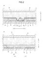
FIG. 2 is a cross-sectional view of the coordinate input device illustrated inFIG. 1 ;FIG. 2(a) is a cross-sectional view taken along Ib-Ib andFIG. 2(b) is a cross-sectional view taken along IIb-IIb. -
FIG. 3 is a cross-sectional view of the coordinate input device illustrated inFIG. 1 taken along IIIb-IIb. -
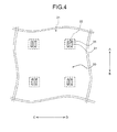
FIG. 4 is a plan view that illustrates a conductive layer and an insulating layer of the coordinate input device illustrated inFIG. 1 . -
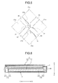
FIG. 5 is an enlarged plan view of the section R ofFIG. 1 . -
FIG. 6 is a cross-sectional view that illustrates a display apparatus with a coordinate input function according to the embodiment of the present invention. -
FIG. 7 is a perspective view that illustrates a liquid crystal display panel. -
FIG. 8 is a plan view that illustrates a coordinate input device according to a second embodiment of the present invention. -
FIG. 9 is a plan view that illustrates an insulating layer and a conductive layer of the coordinate input device illustrated inFIG. 8 . -
FIG. 10 is a cross-sectional view of the coordinate input device illustrated inFIG. 8 taken along IVb-IVb. -
FIG. 11 is a plan view that illustrates a coordinate input device according to a third embodiment of the present invention. - FIG. 12(a) is an exploded plan view that illustrates the side of the substrate of the coordinate input device illustrated in
FIG. 11 ., and FIG. 12(b) is an exploded plan view that illustrates the side of the protective substrate of the coordinate input device illustrated inFIG. 11 . -
FIG. 13 is a cross-sectional view that illustrates a display apparatus with a coordinate input function according to another embodiment of the present invention. -
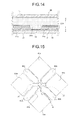
FIG. 14 is a cross-sectional view that illustrates a modified example of the coordinate input device illustrated inFIG. 10 . -
FIG. 15 is a plan view that illustrates a modified example of the coordinate input device illustrated inFIG. 5 . - First, an explanation is given of a capacitive coordinate input device X1 and a display apparatus Y with a coordinate input function according to a first embodiment of the present invention.
- The coordinate input device X1 includes a
substrate 10, aconductive layer 20, aninsulating layer 30, a firstdetection electrode pattern 40, a seconddetection electrode pattern 50, anadjustment pattern 60, ajoint member 70, and aprotective substrate 80. - The
substrate 10 has a function of supporting theconductive layer 20, theinsulating layer 30, the firstdetection electrode pattern 40, the seconddetection electrode pattern 50, and theadjustment pattern 60. As illustrated inFIG. 1 , an exemplary shape of thesubstrate 10 in a planar view is rectangular. The material of thesubstrate 10 has insulation properties and translucency and is, for example, glass or plastic. Here, the translucency means the transmittance of visible light. If glass is used as the material of thesubstrate 10, it is preferable that the thickness of thesubstrate 10 is set to be not less than 0.1 mm and not more than 1.0 mm so that sufficient shape stability is ensured and any change in capacitance is easily detected. - The
conductive layer 20 is formed on or above substantially the entirety of one of the main surfaces of thesubstrate 10. - The
conductive layer 20 includesshield electrodes 21 andsecond connection electrodes 22. - The
shield electrode 21 has a function of reducing the effect of the noise due to, for example, drive signals of a display device, or the like, onfirst detection electrodes 41a andsecond detection electrodes 51a, which will be explained later. Theshield electrode 21 is a continuous layer except for the area of thesecond connection electrode 22 and is set to the reference potential, such as the ground potential. - The
second connection electrode 22 has a function of electrically connecting the adjacent second detection electrodes 52a. As illustrated inFIGS. 2(a), 2(b) , and4 , the circumferential edge of thesecond connection electrode 22 is separated from theshield electrode 21 so that thesecond connection electrode 22 is electrically insulated from theshield electrode 21, and thesecond connection electrodes 22 are dotted like islands. - The material of the
conductive layer 20 has translucency and conductive properties and is, for example, Indium Tin Oxide (ITO), Indium Zinc Oxide (IZO), Antimony Tin Oxide (ATO), Tin Oxide, Zinc Oxide, or the like. - The
insulating layer 30 is formed on or above substantially the entirety of theconductive layer 20. - The
insulating layer 30 has a function of insulating theshield electrode 21 from the firstdetection electrode pattern 40 and insulating theshield electrode 21 from the seconddetection electrode pattern 50. - Furthermore, the
insulating layer 30 includes first through-holes 31. As illustrated inFIGS. 2(a) and4 , the first through-holes 31 are located at positions corresponding to both ends of thesecond connection electrode 22 in theinsulating layer 30 and pass through theinsulating layer 30 in the thickness direction thereof. The material of theinsulating layer 30 has translucency and insulation properties and is, for example, a resin, such as an acrylic resin. - The first
detection electrode patterns 40, the seconddetection electrode patterns 50, and theadjustment patterns 60 are formed on or above theinsulating layer 30. - The first
detection electrode pattern 40 includes firstdetection electrode arrays 41 andwiring conductors 42. - The first
detection electrode array 41 includes thefirst detection electrodes 41a andfirst connection electrodes 41b. Furthermore, the firstdetection electrode array 41 is arranged in the direction of the arrow CD. - The
first detection electrode 41a has a function of detecting, in the direction of the arrow CD, the position of a finger, or the like, that is located close to the input area. Thefirst detection electrodes 41a are arranged with a space interposed therebetween in a matrix in the directions of the arrow AB and the arrow CD. Thefirst detection electrodes 41a, which are adjacent to each other in the direction of the arrow AB, are electrically connected to each other via thefirst connection electrode 41b. As illustrated inFIGS. 1 and5 , thefirst detection electrode 41a according to the present embodiment has a diamond shape in a planar view; however, the shape of thefirst detection electrode 41a is not limited to this. The material of thefirst detection electrode 41a can be the same material as theconductive layer 20. - The
first connection electrode 41b has a function of electrically connecting the adjacentfirst detection electrodes 41a. Furthermore, as illustrated inFIGS. 2(a) and 2(b) , thefirst connection electrode 41b is opposed to thesecond connection electrode 22 with theinsulating layer 30 interposed therebetween. In other words, as illustrated inFIG. 5 , thefirst connection electrode 41b of the firstdetection electrode pattern 40 and thesecond connection electrode 22 of the seconddetection electrode pattern 50 have an intersection area H where thefirst connection electrode 41b intersects with thesecond connection electrode 22 in a planar view. - Moreover, the area of the
first connection electrode 41b in a planar view is set to be smaller than that of thefirst detection electrode 41a in a planar view. - The material of the
first connection electrode 41b can be the same material as theconductive layer 20. - The
wiring conductor 42 has a function of applying a voltage to thefirst detection electrode 41a. As illustrated inFIG. 1 , one end of thewiring conductor 42 is connected to thefirst detection electrode 41a, which is located on the end of the firstdetection electrode array 41, and the other end is positioned on an externalconductive area 11. Thewiring conductor 42 may be connected to both ends of the firstdetection electrode array 41. The material of thewiring conductor 42 has conductive properties and is, for example, a metal, such as aluminum, aluminum alloy, silver, or silver alloy. - The second
detection electrode pattern 50 includes seconddetection electrode arrays 51 andwiring conductors 52.
The seconddetection electrode array 51 includes thesecond detection electrodes 51a and three-dimensional wires 51b. As illustrated inFIG. 1 , the seconddetection electrode array 51 is arranged in the direction of the arrow AB. - The
second detection electrode 51a has a function of detecting, in the direction of the arrow AB, the position of a finger, or the like, that is located close to the input area. Furthermore, thesecond detection electrodes 51a are arranged with a space interposed therebetween in a matrix in the directions of the arrow AB and the arrow CD. As illustrated inFIG. 2(a) , thesecond detection electrodes 51a, which are adjacent to each other in the direction of the arrow CD, are electrically connected to each other via thesecond connection electrode 22 in theconductive layer 20. Thesecond detection electrode 51a has a diamond shape in a planar view; however, the shape of thesecond detection electrode 51a is not limited to this. - The
second detection electrode 51a is located near thefirst detection electrode 41a. This means that the detection electrodes are located, for example, 100 µm to 200 µm apart from each other when viewed in cross section. The material of thesecond detection electrode 51a can be the same material as theconductive layer 20. - The three -
dimensional wire 51b has a function of electrically connecting the adjacentsecond detection electrodes 51a via thesecond connection electrode 22. As illustrated inFIG. 2(a) , the three -dimensional wire 51b is located inside the first through-hole 31 of the insulatinglayer 30. The material of the three-dimensional wire 51b can be the same material as theconductive layer 20. The three-dimensional wire 51b may be formed together with thesecond detection electrode 51a or may be formed individually. - The
wiring conductor 52 has a function of applying a voltage to thesecond detection electrode 51a. As illustrated inFIG. 1 , one end of thewiring conductor 52 is connected to thesecond detection electrode 51a, which is located on the end of the seconddetection electrode array 51, and the other end is positioned on the externalconductive area 11. Thewiring conductor 52 may be connected to both ends of the seconddetection electrode array 51. The material of thewiring conductor 52 can be the same material as thewiring conductor 42. - The
adjustment pattern 60 is located on or above the insulatinglayer 30. As illustrated inFIGS. 1 ,3 , and5 , theadjustment pattern 60 is formed between the adjacentfirst detection electrodes 41a, between the adjacentsecond detection electrodes 51a, and between the adjacent first andsecond detection electrodes adjustment pattern 60 includes the same material as thefirst detection electrode 41a and thesecond detection electrode 51a. - In the coordinate input device X1, the
adjustment pattern 60 is formed, in a planar view, between the adjacentfirst detection electrodes 41a, between the adjacentsecond detection electrodes 51a, and between the adjacent first andsecond detection electrodes detection electrode pattern 40 or the seconddetection electrode pattern 50 is formed and the area where the firstdetection electrode pattern 40 or the seconddetection electrode pattern 50 is not formed. Hence, in the coordinate input device X1, the visible light transmittance and reflectivity can be more uniform for the input area, and the display quality level can be improved, for example, when the coordinate input device X1 is mounted on a display apparatus. - An explanation is given above of a case where the
adjustment pattern 60 is formed between the adjacentfirst detection electrodes 41a, between the adjacentsecond detection electrodes 51a, and between the adjacent first andsecond detection electrodes adjustment layer pattern 60 may be formed between the adjacentfirst detection electrodes 41a, between the adjacentsecond detection electrodes 51a, or between the adjacent first andsecond detection electrodes - It is preferable that the thickness of the
adjustment pattern 60 is substantially the same as that of thefirst detection electrode 41a and thesecond detection electrode 51a, because the visible light transmittance and reflectivity can be more uniform. Here, substantially the same thickness means that the difference in the thickness is, for example, less than or equal to 10 µm. - Furthermore, it is more preferable that the
adjustment pattern 60 has the same visible light transmittance and reflectivity as those of thefirst detection electrode 41a and thesecond detection electrode 51a. Here, the same visible light transmittance and reflectivity means that the difference between the visible light transmittance and reflectivity of theadjustment pattern 60 and the visible light transmittance and reflectivity of thefirst detection electrode 41a and thesecond detection electrode 51a is in the range of ± 10% of the visible light transmittance and reflectivity of thefirst detection electrode 41a and thesecond detection electrode 51a that are used as a reference. - As illustrated in
FIG. 5 , theadjustment pattern 60 has asharp edge 60a whose width becomes narrower as it approaches the intersection area H of the firstdetection electrode pattern 40 and the seconddetection electrode pattern 50. Thus, it is possible to form theadjustment pattern 60 at a narrow area near the intersection area H and to locate theadjustment pattern 60 near the intersection area H of the firstdetection electrode pattern 40 and the seconddetection electrode pattern 50. - The
adjustment pattern 60 is located on or above the insulatinglayer 30 on which thefirst detection electrode 41a and thesecond detection electrode 51a are formed. Thus, it is possible to form theadjustment pattern 60 at the same time thefirst detection electrode 41a and thesecond detection electrode 51a are formed, which is preferable because the productivity of the coordinate input device X1 is improved. - The
joint member 70 has a function of attaching theprotective substrate 80 to the insulatinglayer 30 on which the firstdetection electrode pattern 40 and the seconddetection electrode pattern 50 have been formed. The material of thejoint member 70 can be, for example, an epoxy resin, and the like. - The
protective substrate 80 has a function of preventing direct contact of the firstdetection electrode pattern 40 and the seconddetection electrode pattern 50 with an external object. Examples of the material of theprotective substrate 80 include acrylic or glass, which has favorable transparency to visible light. - In the coordinate input device X1, a conductive body, such as a finger, is pressed against or located close to the
protective substrate 80 so that the location where the conductive body is pressed against or located close to is detected as the input location. Specifically, if the conductive body is pressed against or located close to the input area, the capacitance obtained between the conductive body and the first andsecond detection electrodes - Next, an explanation is given of the display apparatus Y with a coordinate input function, which includes the coordinate input device X1.
- As illustrated in
FIG. 6 , the display apparatus Y with a coordinate input function includes the coordinate input device X1 and a display device Z. Furthermore, the display device Z includes a liquidcrystal display panel 90, alight source device 100, and achassis 110. - The liquid
crystal display panel 90 is arranged such that it is opposed to thefirst detection electrodes 41a, thesecond detection electrodes 51a, and theadjustment patterns 60 of the coordinate input device X1. - As illustrated in
FIG. 7 , the liquidcrystal display panel 90 includes afirst base 91, asecond base 92, and a sealingmember 93. A crystal liquid layer (not illustrated) is interposed between thefirst base 91 and thesecond base 92 and is sealed with the sealingmember 93 so that a display area DA is formed that includes a plurality of pixels for displaying an image. - The
light source device 100 has a function of emitting light toward the liquidcrystal display panel 90 and is located under the liquidcrystal display panel 90. - The
chassis 110 is a member that contains the liquidcrystal display panel 90 and thelight source device 100. Thechassis 110 includes anupper chassis 111 and alower chassis 112. The material of thechassis 110 can be a resin, such as a. polycarbonate resin, or a metal, such as stainless steel or aluminum. - The coordinate input device X1 is attached to the display device Z with a double-sided tape T. An attaching member that is used as a method of attaching the coordinate input device X1 to the display device Z is not limited to the double-sided tape T and may be an adhesive material, such as a thermo-setting resin or an ultraviolet curable resin, or a fixing structure that physically fixes the coordinate input device X1 to the display device Z.
- The display apparatus Y with a coordinate input function according to the present invention includes the coordinate input device X1, as described above. Thus, the display quality level of a product can be improved.
- Next, an explanation is given, with reference to
FIGS. 8 to 10 , of a coordinate input device X2 according to a second embodiment of the present invention. - The coordinate input device X2 is different from the coordinate input device X1 in that an insulating
layer 30A is used instead of the insulatinglayer 30. An explanation is omitted for the duplicate sections of the coordinate input device X1 and the coordinate input device X2. - As illustrated in
FIG. 9 , the insulatinglayer 30A includes first through-holes 31A and second through-holes 32A. The first through-holes 31A are located at positions corresponding to both ends of thesecond connection electrode 22 in the insulatinglayer 30A and pass through the insulatinglayer 30A in the thickness direction thereof. As illustrated inFIG. 10 , the second through-hole 32A is located at an area corresponding to theshield electrode 21 in the insulatinglayer 30, and a conductive member is arranged, at least, on the inner wall surface of the second through-hole 32A. - As illustrated in
FIG. 10 , theadjustment pattern 60 is electrically connected to theshield electrode 21 via the conductive member of the second through-hole 32A in the insulatinglayer 30A. Specifically, the second through-hole 32A functions as a conduction through-hole. A method for electrically connecting theadjustment pattern 60 to theshield electrode 21 is not limited to the method using the conduction through-hole. - In the coordinate input device X2, the
adjustment pattern 60 is electrically connected to theshield electrode 21 via the conductive member of the second through-hole 32A in the insulatinglayer 30A. Thus, it is possible to release the floating charge, which occurs between thefirst detection electrode 41a and thesecond detection electrode 51a, to theshield electrode 21 through theadjustment pattern 60. Hence, it is possible to improve the position detection sensitivity of thefirst detection electrode 41a and thesecond detection electrode 51a. - In the coordinate input device X2, the
adjustment pattern 60 is located on or above the insulatinglayer 30A. Specifically, theadjustment pattern 60 is located on the same level as thefirst detection electrode 41a and thesecond detection electrode 51a so that theadjustment pattern 60 can be located closer to thefirst detection electrode 41a and thesecond detection electrode 51a; thus, it is possible to easily release the floating charge, which occurs between thefirst detection electrode 41a and thesecond detection electrode 51a, to theshield electrode 21 through the adjustment pattern. 60. - The display apparatus Y with a coordinate input function may use the coordinate input device X2 instead of the coordinate input device X1.
- Next, an explanation is given, with reference to
FIGS. 11 and12 , of a coordinate input device X3 according to a third embodiment of the present invention. - The coordinate input device X3 includes the
substrate 10, the firstdetection electrode pattern 40, a seconddetection electrode pattern 50B, theadjustment pattern 60, thejoint member 70, and theprotective substrate 80. An explanation is omitted for the duplicate sections of the coordinate input device X1 and the coordinate input device X3. - As illustrated in FIG. 12(b), the second
detection electrode pattern 50B includes seconddetection electrode arrays 51B andwiring conductors 52B and is formed on or above one of the main surfaces of theprotective substrate 80. The seconddetection electrode array 51B includes second detection electrodes 51Ba and second connection electrodes 51Bb, and the seconddetection electrode array 51B is arranged in the direction of the arrow AB. - As illustrated in
FIG. 11 , in the coordinate input device X3, thesubstrate 10 is attached to theprotective substrate 80 with thejoint member 70 such that thefirst detection electrodes 41a are not overlapped with the second detection electrodes 51Ba in a planar view. - The
adjustment pattern 60 is formed such that, when thesubstrate 10 is attached to theprotective substrate 80, theadjustment pattern 60 is located between thefirst detection electrode 41a and the second detection electrode 51Ba in a planar view. Theadjustment pattern 60 is formed on or above thesubstrate 10 according to the present embodiment; however, theadjustment pattern 60 may be formed on or above theprotective substrate 80 or may be formed on or above both thesubstrate 10 and theprotective substrate 80. - The coordinate input device X3 produces the same advantage as that described for the coordinate input device X1.
- The display apparatus Y with a coordinate input function may use the coordinate input device X3 instead of the coordinate input device X1.
- The specific embodiments of the present invention are described above; however, the present invention is not limited to these.
- In the coordinate input devices X1, X2, the
first connection electrode 41b is electrically insulated from thesecond connection electrode 22 because thefirst connection electrode 41b is opposed to thesecond connection electrode 22 via the insulatinglayer - Although the
joint member 70 and theprotective substrate 80 are provided in the coordinate input devices X1, X2, they may not be provided. - Although the
shield electrode 21 is provided in the coordinate input devices X1, X2, it may not be provided. - In the coordinate input devices X1, X2, the
conductive layer 20, the insulatinglayer 30, and the firstdetection electrode pattern 40 and the seconddetection electrode pattern 50 are laminated in this order on or above one of the main surfaces of thesubstrate 10; however, the firstdetection electrode pattern 40 and the seconddetection electrode pattern 50, the insulatinglayer 30, and theconductive layer 20 may be laminated in this order on or above one of the main surfaces of thesubstrate 10.
In this case, as illustrated inFIG. 13 , when one of the coordinate input devices X1, X2 is mounted on the display apparatus Z, the upper substrate of the display device Y may be used as a protective substrate. - In the coordinate input devices X1, X2, the
adjustment pattern 60 is located away from thefirst detection electrode 41a and thesecond detection electrode 51a; however, the present invention is not limited to this, and a configuration may be appropriate if they are electrically insulated from each other. For example, theadjustment pattern 60 may be covered with an insulating layer. - In the coordinate input device X2, the
adjustment pattern 60 is electrically connected to theshield electrode 21 via the second through-hole 32A of the insulatinglayer 30A; however, as illustrated inFIG. 14 , theadjustment pattern 60 may be directly formed on theshield electrode 21 within the second through-hole 32A. - The
shield electrode 21 may be provided in the coordinate input device X3. It is preferable to provide theshield electrode 21 because it is possible to reduce the effect of noise, which occurs due to the drive signals of the display device, on thedetection electrodes - In the coordinate input devices X1, X2, X3, an
adjustment pattern 60A may be provided instead of theadjustment pattern 60. Here, theadjustment pattern 60A has circular edges. This is preferable because the circular areas easily scatter transmitted light and reflected light and theadjustment pattern 60A is hardly visible. - Although the capacitive coordinate input device is explained as the touch panels X1, X2, X3, the present invention is not limited to this. For example, the present invention may be also applied to a resistive coordinate input device.
- Although an explanation is given of a case where the display panel of the display apparatus Y is the liquid
crystal display panel 90, the present invention is not limited to this. Specifically, the display panel may be a CRT, plasma display, organic EL display, inorganic EL display, LED display, fluorescent display tube, field emission display, surface-conduction electron-emitter display, electronic paper, or the like. -
- X1, X2, X3 coordinate input device
- Y display apparatus with a coordinate input function
- Z display device
- 10 substrate
- 20 conductive layer
- 30, 30A insulating layer
- 40 first detection electrode pattern
- 50, 50B second detection electrode pattern
- 60, 60A adjustment pattern
- 70 joint member
- 80 protective substrate
- 90 liquid crystal display panel
- 100 light source device
- 110 chassis
Claims (12)
- A coordinate input device comprising:a translucent substrate;a detection electrode pattern that includes a plurality of detection electrodes for detecting an input location, the detection electrodes being arranged on or above the translucent substrate in at least one direction; andan adjustment pattern that is formed between the detection electrodes in a planar view and is electrically insulated from the detection electrodes, the adjustment pattern including the same material as the detection electrodes.
- The coordinate input device according to claim. 1, further comprising;
a conductive layer that is set to the reference potential; and
an insulating layer, the conductive layer and the insulating layer being sequentially laminated on or above the translucent substrate, wherein
the detection electrodes and the adjustment pattern are located on or above the insulating layer, and
the adjustment pattern includes a conductive material and is electrically connected to the conductive layer. - The coordinate input device according to claim 2, wherein
the insulating layer has a conduction through-hole that passes through the insulating layer in the thickness direction thereof, and
the adjustment pattern and the conductive layer are connected to each other via the conduction through-hole. - The coordinate input device according to claim 1, further comprising;
a conductive layer that is set to the reference potential; and
an insulating layer, the conductive layer and the insulating layer being sequentially laminated on or above the translucent substrate, wherein
the detection electrodes are located on or above the insulating layer, and
the adjustment pattern includes a conductive material and is located on or above the conductive layer. - The coordinate input device according to claim 4, wherein
the insulating layer has a through-hole that passes through the insulating layer in the thickness direction thereof, and
the adjustment pattern is formed on or above the conductive layer within the through-hole. - The coordinate input device according to claim 1, wherein the thickness of the adjustment pattern is substantially the same as that of the detection electrode.
- The coordinate input device according to claim 1, wherein
the detection electrode pattern includes a first detection electrode pattern that is arranged in a first direction and a second detection electrode pattern that is arranged in a second direction, and
the adjustment pattern is located, in a planar view, between the adjacent first detection electrodes, between the adjacent second detection electrodes, and between the adjacent first and second detection electrodes. - A coordinate input device comprising:a translucent substrate;a detection electrode pattern that includes a plurality of detection electrodes for detecting an input location, the detection electrodes being arranged on or above the translucent substrate in at least one direction; andan adjustment pattern that is formed between the detection electrodes in a planar view and is electrically insulated from the detection electrodes, the adjustment pattern having the same optical translucency as that of the detection electrodes.
- A coordinate input device comprising:a translucent substrate;a detection electrode pattern that includes a plurality of detection electrodes for detecting an input location, the detection electrodes being arranged on or above the translucent substrate in at least one direction; andan adjustment pattern that is formed between the detection electrodes in a planar view and is electrically insulated from the detection electrodes, the adjustment pattern having the same optical reflectivity as that of the detection electrodes.
- The coordinate input device according to claim 1, wherein
the detection electrode pattern includes a first detection electrode pattern that is arranged in a first direction and a second detection electrode pattern that is arranged in a second direction,
the first detection electrode pattern arranged in the first direction and the second detection pattern arranged in the second direction have an intersection area where the first and second detection electrode patterns intersect with each other, and
the adjustment pattern has a sharp edge that becomes narrow in a planar view as the adjustment pattern approaches the intersection area. - The coordinate input device according to claim 1, wherein the adjustment pattern has a circular edge in a planar view.
- A display apparatus with a coordinate input function, comprising:the coordinate input device according to claim 1; anda display panel that is opposed to the detection electrodes and the adjustment pattern of the coordinate input device.
Applications Claiming Priority (2)
| Application Number | Priority Date | Filing Date | Title |
|---|---|---|---|
| JP2009154783 | 2009-06-30 | ||
| PCT/JP2010/060943 WO2011001925A1 (en) | 2009-06-30 | 2010-06-28 | Coordinate input device and display device having coordinate input function |
Publications (3)
| Publication Number | Publication Date |
|---|---|
| EP2450778A1 true EP2450778A1 (en) | 2012-05-09 |
| EP2450778A4 EP2450778A4 (en) | 2015-07-22 |
| EP2450778B1 EP2450778B1 (en) | 2019-04-17 |
Family
ID=43411001
Family Applications (1)
| Application Number | Title | Priority Date | Filing Date |
|---|---|---|---|
| EP10794094.2A Not-in-force EP2450778B1 (en) | 2009-06-30 | 2010-06-28 | Coordinate input device and display device having coordinate input function |
Country Status (5)
| Country | Link |
|---|---|
| US (1) | US20120075230A1 (en) |
| EP (1) | EP2450778B1 (en) |
| JP (1) | JP5442012B2 (en) |
| CN (1) | CN102449581A (en) |
| WO (1) | WO2011001925A1 (en) |
Families Citing this family (11)
| Publication number | Priority date | Publication date | Assignee | Title |
|---|---|---|---|---|
| TWI423092B (en) * | 2010-10-04 | 2014-01-11 | Au Optronics Corp | Touch panel and repairing method thereof |
| JP2013012182A (en) * | 2011-05-27 | 2013-01-17 | Kyocera Corp | Input unit, display unit, and electronic device |
| US9634660B2 (en) * | 2011-12-20 | 2017-04-25 | Atmel Corporation | Touch sensor with reduced anti-touch effects |
| WO2013107471A1 (en) * | 2012-01-19 | 2013-07-25 | Sony Ericsson Mobile Communications Ab | Touch panel |
| CN103294294B (en) | 2012-08-17 | 2018-01-19 | 上海天马微电子有限公司 | Touch sensor, built-in touch LCD panel, liquid crystal display |
| JP6253923B2 (en) * | 2013-08-30 | 2017-12-27 | 株式会社ジャパンディスプレイ | Organic electroluminescence device with built-in touch sensor |
| KR102227078B1 (en) * | 2014-03-26 | 2021-03-16 | 한국전자통신연구원 | Touch panel |
| CN106249975B (en) * | 2016-08-12 | 2018-11-06 | 京东方科技集团股份有限公司 | A kind of touch screen, display device and touch screen manufacturing method |
| CN107704135A (en) * | 2017-10-12 | 2018-02-16 | 京东方科技集团股份有限公司 | A kind of contact panel and preparation method thereof, touch control display apparatus |
| CN110007808B (en) | 2017-12-29 | 2022-10-18 | 乐金显示有限公司 | Electroluminescent display including touch sensor |
| KR102770672B1 (en) | 2018-10-09 | 2025-02-24 | 에씰로 앙터나시오날 | Methods for adapting ocular devices to the wearer's visual exploration strategy |
Family Cites Families (18)
| Publication number | Priority date | Publication date | Assignee | Title |
|---|---|---|---|---|
| JPH05224818A (en) * | 1992-02-10 | 1993-09-03 | Matsushita Electric Ind Co Ltd | Touch panel device |
| US6147680A (en) * | 1997-06-03 | 2000-11-14 | Koa T&T Corporation | Touchpad with interleaved traces |
| US7663607B2 (en) * | 2004-05-06 | 2010-02-16 | Apple Inc. | Multipoint touchscreen |
| JP2003099185A (en) * | 2001-09-20 | 2003-04-04 | Alps Electric Co Ltd | Input device |
| US7129935B2 (en) * | 2003-06-02 | 2006-10-31 | Synaptics Incorporated | Sensor patterns for a capacitive sensing apparatus |
| US20050030048A1 (en) * | 2003-08-05 | 2005-02-10 | Bolender Robert J. | Capacitive sensing device for use in a keypad assembly |
| JP2006011523A (en) * | 2004-06-22 | 2006-01-12 | Three M Innovative Properties Co | Touch panel sensor |
| US7394458B2 (en) * | 2004-09-24 | 2008-07-01 | Apple Inc. | Low EMI capacitive trackpad |
| JP4500159B2 (en) * | 2004-12-22 | 2010-07-14 | 日東電工株式会社 | Transparent conductive laminate and touch panel provided with the same |
| JP2008129708A (en) * | 2006-11-17 | 2008-06-05 | Alps Electric Co Ltd | Transparent touch panel and its manufacturing method |
| JP4153009B2 (en) * | 2007-02-15 | 2008-09-17 | アルプス電気株式会社 | Input device |
| US20080309633A1 (en) * | 2007-06-13 | 2008-12-18 | Apple Inc. | Touch-sensitive display |
| TWI367437B (en) * | 2007-09-29 | 2012-07-01 | Au Optronics Corp | Touch panel and manufacturing method thereof |
| CN100495139C (en) * | 2007-10-10 | 2009-06-03 | 友达光电股份有限公司 | Touch panel and manufacturing method thereof |
| JP4945483B2 (en) * | 2008-02-27 | 2012-06-06 | 株式会社 日立ディスプレイズ | Display panel |
| JP4720857B2 (en) * | 2008-06-18 | 2011-07-13 | ソニー株式会社 | Capacitance type input device and display device with input function |
| US20100045625A1 (en) * | 2008-08-21 | 2010-02-25 | Tpo Displays Corp. | Touch panel and system for displaying images utilizing the same |
| US8593410B2 (en) * | 2009-04-10 | 2013-11-26 | Apple Inc. | Touch sensor panel design |
-
2010
- 2010-06-28 CN CN2010800227744A patent/CN102449581A/en active Pending
- 2010-06-28 EP EP10794094.2A patent/EP2450778B1/en not_active Not-in-force
- 2010-06-28 JP JP2011520904A patent/JP5442012B2/en active Active
- 2010-06-28 US US13/375,205 patent/US20120075230A1/en not_active Abandoned
- 2010-06-28 WO PCT/JP2010/060943 patent/WO2011001925A1/en not_active Ceased
Non-Patent Citations (1)
| Title |
|---|
| See references of WO2011001925A1 * |
Also Published As
| Publication number | Publication date |
|---|---|
| EP2450778A4 (en) | 2015-07-22 |
| JPWO2011001925A1 (en) | 2012-12-13 |
| JP5442012B2 (en) | 2014-03-12 |
| EP2450778B1 (en) | 2019-04-17 |
| WO2011001925A1 (en) | 2011-01-06 |
| CN102449581A (en) | 2012-05-09 |
| US20120075230A1 (en) | 2012-03-29 |
Similar Documents
| Publication | Publication Date | Title |
|---|---|---|
| EP2450778A1 (en) | Coordinate input device and display device having coordinate input function | |
| US12517618B2 (en) | Touch input device | |
| US11182000B2 (en) | Smartphone | |
| US10162445B2 (en) | Electrode sheet for pressure detection and pressure detecting module including the same | |
| JP5448886B2 (en) | Input device and display device having the same | |
| EP2541381B1 (en) | Input device, display device, and portable terminal | |
| WO2026009496A1 (en) | Touch sensor | |
| KR20150125477A (en) | Touch panel and touch device with the same |
Legal Events
| Date | Code | Title | Description |
|---|---|---|---|
| PUAI | Public reference made under article 153(3) epc to a published international application that has entered the european phase |
Free format text: ORIGINAL CODE: 0009012 |
|
| 17P | Request for examination filed |
Effective date: 20111130 |
|
| AK | Designated contracting states |
Kind code of ref document: A1 Designated state(s): AL AT BE BG CH CY CZ DE DK EE ES FI FR GB GR HR HU IE IS IT LI LT LU LV MC MK MT NL NO PL PT RO SE SI SK SM TR |
|
| DAX | Request for extension of the european patent (deleted) | ||
| RA4 | Supplementary search report drawn up and despatched (corrected) |
Effective date: 20150619 |
|
| RIC1 | Information provided on ipc code assigned before grant |
Ipc: G06F 3/044 20060101ALI20150615BHEP Ipc: G06F 3/041 20060101AFI20150615BHEP |
|
| STAA | Information on the status of an ep patent application or granted ep patent |
Free format text: STATUS: EXAMINATION IS IN PROGRESS |
|
| 17Q | First examination report despatched |
Effective date: 20171219 |
|
| GRAP | Despatch of communication of intention to grant a patent |
Free format text: ORIGINAL CODE: EPIDOSNIGR1 |
|
| STAA | Information on the status of an ep patent application or granted ep patent |
Free format text: STATUS: GRANT OF PATENT IS INTENDED |
|
| INTG | Intention to grant announced |
Effective date: 20181113 |
|
| GRAS | Grant fee paid |
Free format text: ORIGINAL CODE: EPIDOSNIGR3 |
|
| GRAA | (expected) grant |
Free format text: ORIGINAL CODE: 0009210 |
|
| STAA | Information on the status of an ep patent application or granted ep patent |
Free format text: STATUS: THE PATENT HAS BEEN GRANTED |
|
| AK | Designated contracting states |
Kind code of ref document: B1 Designated state(s): AL AT BE BG CH CY CZ DE DK EE ES FI FR GB GR HR HU IE IS IT LI LT LU LV MC MK MT NL NO PL PT RO SE SI SK SM TR |
|
| REG | Reference to a national code |
Ref country code: GB Ref legal event code: FG4D |
|
| REG | Reference to a national code |
Ref country code: CH Ref legal event code: EP |
|
| REG | Reference to a national code |
Ref country code: DE Ref legal event code: R096 Ref document number: 602010058319 Country of ref document: DE |
|
| REG | Reference to a national code |
Ref country code: AT Ref legal event code: REF Ref document number: 1122289 Country of ref document: AT Kind code of ref document: T Effective date: 20190515 Ref country code: IE Ref legal event code: FG4D |
|
| REG | Reference to a national code |
Ref country code: NL Ref legal event code: MP Effective date: 20190417 |
|
| REG | Reference to a national code |
Ref country code: LT Ref legal event code: MG4D |
|
| PG25 | Lapsed in a contracting state [announced via postgrant information from national office to epo] |
Ref country code: NL Free format text: LAPSE BECAUSE OF FAILURE TO SUBMIT A TRANSLATION OF THE DESCRIPTION OR TO PAY THE FEE WITHIN THE PRESCRIBED TIME-LIMIT Effective date: 20190417 |
|
| PG25 | Lapsed in a contracting state [announced via postgrant information from national office to epo] |
Ref country code: ES Free format text: LAPSE BECAUSE OF FAILURE TO SUBMIT A TRANSLATION OF THE DESCRIPTION OR TO PAY THE FEE WITHIN THE PRESCRIBED TIME-LIMIT Effective date: 20190417 Ref country code: LT Free format text: LAPSE BECAUSE OF FAILURE TO SUBMIT A TRANSLATION OF THE DESCRIPTION OR TO PAY THE FEE WITHIN THE PRESCRIBED TIME-LIMIT Effective date: 20190417 Ref country code: NO Free format text: LAPSE BECAUSE OF FAILURE TO SUBMIT A TRANSLATION OF THE DESCRIPTION OR TO PAY THE FEE WITHIN THE PRESCRIBED TIME-LIMIT Effective date: 20190717 Ref country code: HR Free format text: LAPSE BECAUSE OF FAILURE TO SUBMIT A TRANSLATION OF THE DESCRIPTION OR TO PAY THE FEE WITHIN THE PRESCRIBED TIME-LIMIT Effective date: 20190417 Ref country code: SE Free format text: LAPSE BECAUSE OF FAILURE TO SUBMIT A TRANSLATION OF THE DESCRIPTION OR TO PAY THE FEE WITHIN THE PRESCRIBED TIME-LIMIT Effective date: 20190417 Ref country code: PT Free format text: LAPSE BECAUSE OF FAILURE TO SUBMIT A TRANSLATION OF THE DESCRIPTION OR TO PAY THE FEE WITHIN THE PRESCRIBED TIME-LIMIT Effective date: 20190817 Ref country code: FI Free format text: LAPSE BECAUSE OF FAILURE TO SUBMIT A TRANSLATION OF THE DESCRIPTION OR TO PAY THE FEE WITHIN THE PRESCRIBED TIME-LIMIT Effective date: 20190417 Ref country code: AL Free format text: LAPSE BECAUSE OF FAILURE TO SUBMIT A TRANSLATION OF THE DESCRIPTION OR TO PAY THE FEE WITHIN THE PRESCRIBED TIME-LIMIT Effective date: 20190417 |
|
| PG25 | Lapsed in a contracting state [announced via postgrant information from national office to epo] |
Ref country code: LV Free format text: LAPSE BECAUSE OF FAILURE TO SUBMIT A TRANSLATION OF THE DESCRIPTION OR TO PAY THE FEE WITHIN THE PRESCRIBED TIME-LIMIT Effective date: 20190417 Ref country code: PL Free format text: LAPSE BECAUSE OF FAILURE TO SUBMIT A TRANSLATION OF THE DESCRIPTION OR TO PAY THE FEE WITHIN THE PRESCRIBED TIME-LIMIT Effective date: 20190417 Ref country code: GR Free format text: LAPSE BECAUSE OF FAILURE TO SUBMIT A TRANSLATION OF THE DESCRIPTION OR TO PAY THE FEE WITHIN THE PRESCRIBED TIME-LIMIT Effective date: 20190718 Ref country code: BG Free format text: LAPSE BECAUSE OF FAILURE TO SUBMIT A TRANSLATION OF THE DESCRIPTION OR TO PAY THE FEE WITHIN THE PRESCRIBED TIME-LIMIT Effective date: 20190717 |
|
| REG | Reference to a national code |
Ref country code: AT Ref legal event code: MK05 Ref document number: 1122289 Country of ref document: AT Kind code of ref document: T Effective date: 20190417 |
|
| PG25 | Lapsed in a contracting state [announced via postgrant information from national office to epo] |
Ref country code: IS Free format text: LAPSE BECAUSE OF FAILURE TO SUBMIT A TRANSLATION OF THE DESCRIPTION OR TO PAY THE FEE WITHIN THE PRESCRIBED TIME-LIMIT Effective date: 20190817 |
|
| REG | Reference to a national code |
Ref country code: DE Ref legal event code: R097 Ref document number: 602010058319 Country of ref document: DE |
|
| PG25 | Lapsed in a contracting state [announced via postgrant information from national office to epo] |
Ref country code: MC Free format text: LAPSE BECAUSE OF FAILURE TO SUBMIT A TRANSLATION OF THE DESCRIPTION OR TO PAY THE FEE WITHIN THE PRESCRIBED TIME-LIMIT Effective date: 20190417 Ref country code: CZ Free format text: LAPSE BECAUSE OF FAILURE TO SUBMIT A TRANSLATION OF THE DESCRIPTION OR TO PAY THE FEE WITHIN THE PRESCRIBED TIME-LIMIT Effective date: 20190417 Ref country code: RO Free format text: LAPSE BECAUSE OF FAILURE TO SUBMIT A TRANSLATION OF THE DESCRIPTION OR TO PAY THE FEE WITHIN THE PRESCRIBED TIME-LIMIT Effective date: 20190417 Ref country code: SK Free format text: LAPSE BECAUSE OF FAILURE TO SUBMIT A TRANSLATION OF THE DESCRIPTION OR TO PAY THE FEE WITHIN THE PRESCRIBED TIME-LIMIT Effective date: 20190417 Ref country code: DK Free format text: LAPSE BECAUSE OF FAILURE TO SUBMIT A TRANSLATION OF THE DESCRIPTION OR TO PAY THE FEE WITHIN THE PRESCRIBED TIME-LIMIT Effective date: 20190417 Ref country code: AT Free format text: LAPSE BECAUSE OF FAILURE TO SUBMIT A TRANSLATION OF THE DESCRIPTION OR TO PAY THE FEE WITHIN THE PRESCRIBED TIME-LIMIT Effective date: 20190417 Ref country code: EE Free format text: LAPSE BECAUSE OF FAILURE TO SUBMIT A TRANSLATION OF THE DESCRIPTION OR TO PAY THE FEE WITHIN THE PRESCRIBED TIME-LIMIT Effective date: 20190417 |
|
| REG | Reference to a national code |
Ref country code: CH Ref legal event code: PL |
|
| PLBE | No opposition filed within time limit |
Free format text: ORIGINAL CODE: 0009261 |
|
| STAA | Information on the status of an ep patent application or granted ep patent |
Free format text: STATUS: NO OPPOSITION FILED WITHIN TIME LIMIT |
|
| PG25 | Lapsed in a contracting state [announced via postgrant information from national office to epo] |
Ref country code: IT Free format text: LAPSE BECAUSE OF FAILURE TO SUBMIT A TRANSLATION OF THE DESCRIPTION OR TO PAY THE FEE WITHIN THE PRESCRIBED TIME-LIMIT Effective date: 20190417 Ref country code: SM Free format text: LAPSE BECAUSE OF FAILURE TO SUBMIT A TRANSLATION OF THE DESCRIPTION OR TO PAY THE FEE WITHIN THE PRESCRIBED TIME-LIMIT Effective date: 20190417 |
|
| 26N | No opposition filed |
Effective date: 20200120 |
|
| GBPC | Gb: european patent ceased through non-payment of renewal fee |
Effective date: 20190717 |
|
| REG | Reference to a national code |
Ref country code: BE Ref legal event code: MM Effective date: 20190630 |
|
| PG25 | Lapsed in a contracting state [announced via postgrant information from national office to epo] |
Ref country code: TR Free format text: LAPSE BECAUSE OF FAILURE TO SUBMIT A TRANSLATION OF THE DESCRIPTION OR TO PAY THE FEE WITHIN THE PRESCRIBED TIME-LIMIT Effective date: 20190417 |
|
| PG25 | Lapsed in a contracting state [announced via postgrant information from national office to epo] |
Ref country code: GB Free format text: LAPSE BECAUSE OF NON-PAYMENT OF DUE FEES Effective date: 20190717 Ref country code: IE Free format text: LAPSE BECAUSE OF NON-PAYMENT OF DUE FEES Effective date: 20190628 |
|
| PG25 | Lapsed in a contracting state [announced via postgrant information from national office to epo] |
Ref country code: LI Free format text: LAPSE BECAUSE OF NON-PAYMENT OF DUE FEES Effective date: 20190630 Ref country code: CH Free format text: LAPSE BECAUSE OF NON-PAYMENT OF DUE FEES Effective date: 20190630 Ref country code: LU Free format text: LAPSE BECAUSE OF NON-PAYMENT OF DUE FEES Effective date: 20190628 Ref country code: BE Free format text: LAPSE BECAUSE OF NON-PAYMENT OF DUE FEES Effective date: 20190630 Ref country code: SI Free format text: LAPSE BECAUSE OF FAILURE TO SUBMIT A TRANSLATION OF THE DESCRIPTION OR TO PAY THE FEE WITHIN THE PRESCRIBED TIME-LIMIT Effective date: 20190417 |
|
| PG25 | Lapsed in a contracting state [announced via postgrant information from national office to epo] |
Ref country code: FR Free format text: LAPSE BECAUSE OF NON-PAYMENT OF DUE FEES Effective date: 20190630 |
|
| PG25 | Lapsed in a contracting state [announced via postgrant information from national office to epo] |
Ref country code: CY Free format text: LAPSE BECAUSE OF FAILURE TO SUBMIT A TRANSLATION OF THE DESCRIPTION OR TO PAY THE FEE WITHIN THE PRESCRIBED TIME-LIMIT Effective date: 20190417 |
|
| PG25 | Lapsed in a contracting state [announced via postgrant information from national office to epo] |
Ref country code: MT Free format text: LAPSE BECAUSE OF FAILURE TO SUBMIT A TRANSLATION OF THE DESCRIPTION OR TO PAY THE FEE WITHIN THE PRESCRIBED TIME-LIMIT Effective date: 20190417 Ref country code: HU Free format text: LAPSE BECAUSE OF FAILURE TO SUBMIT A TRANSLATION OF THE DESCRIPTION OR TO PAY THE FEE WITHIN THE PRESCRIBED TIME-LIMIT; INVALID AB INITIO Effective date: 20100628 |
|
| PG25 | Lapsed in a contracting state [announced via postgrant information from national office to epo] |
Ref country code: MK Free format text: LAPSE BECAUSE OF FAILURE TO SUBMIT A TRANSLATION OF THE DESCRIPTION OR TO PAY THE FEE WITHIN THE PRESCRIBED TIME-LIMIT Effective date: 20190417 |
|
| P01 | Opt-out of the competence of the unified patent court (upc) registered |
Effective date: 20230508 |
|
| PGFP | Annual fee paid to national office [announced via postgrant information from national office to epo] |
Ref country code: DE Payment date: 20230502 Year of fee payment: 14 |
|
| REG | Reference to a national code |
Ref country code: DE Ref legal event code: R119 Ref document number: 602010058319 Country of ref document: DE |
|
| PG25 | Lapsed in a contracting state [announced via postgrant information from national office to epo] |
Ref country code: DE Free format text: LAPSE BECAUSE OF NON-PAYMENT OF DUE FEES Effective date: 20250101 |