EP2448070A1 - Socket and motherboard with the same - Google Patents
Socket and motherboard with the same Download PDFInfo
- Publication number
- EP2448070A1 EP2448070A1 EP10189002A EP10189002A EP2448070A1 EP 2448070 A1 EP2448070 A1 EP 2448070A1 EP 10189002 A EP10189002 A EP 10189002A EP 10189002 A EP10189002 A EP 10189002A EP 2448070 A1 EP2448070 A1 EP 2448070A1
- Authority
- EP
- European Patent Office
- Prior art keywords
- socket
- latch
- side plate
- axle
- fastening portion
- Prior art date
- Legal status (The legal status is an assumption and is not a legal conclusion. Google has not performed a legal analysis and makes no representation as to the accuracy of the status listed.)
- Granted
Links
- 230000009977 dual effect Effects 0.000 description 3
- 238000002347 injection Methods 0.000 description 3
- 239000007924 injection Substances 0.000 description 3
- 238000012986 modification Methods 0.000 description 2
- 230000004048 modification Effects 0.000 description 2
- 238000010276 construction Methods 0.000 description 1
- 238000000605 extraction Methods 0.000 description 1
- 230000006870 function Effects 0.000 description 1
- 238000000034 method Methods 0.000 description 1
- 239000002699 waste material Substances 0.000 description 1
Images




Classifications
-
- H—ELECTRICITY
- H01—ELECTRIC ELEMENTS
- H01R—ELECTRICALLY-CONDUCTIVE CONNECTIONS; STRUCTURAL ASSOCIATIONS OF A PLURALITY OF MUTUALLY-INSULATED ELECTRICAL CONNECTING ELEMENTS; COUPLING DEVICES; CURRENT COLLECTORS
- H01R12/00—Structural associations of a plurality of mutually-insulated electrical connecting elements, specially adapted for printed circuits, e.g. printed circuit boards [PCB], flat or ribbon cables, or like generally planar structures, e.g. terminal strips, terminal blocks; Coupling devices specially adapted for printed circuits, flat or ribbon cables, or like generally planar structures; Terminals specially adapted for contact with, or insertion into, printed circuits, flat or ribbon cables, or like generally planar structures
- H01R12/70—Coupling devices
- H01R12/7005—Guiding, mounting, polarizing or locking means; Extractors
- H01R12/7011—Locking or fixing a connector to a PCB
- H01R12/7017—Snap means
- H01R12/7029—Snap means not integral with the coupling device
-
- H—ELECTRICITY
- H01—ELECTRIC ELEMENTS
- H01R—ELECTRICALLY-CONDUCTIVE CONNECTIONS; STRUCTURAL ASSOCIATIONS OF A PLURALITY OF MUTUALLY-INSULATED ELECTRICAL CONNECTING ELEMENTS; COUPLING DEVICES; CURRENT COLLECTORS
- H01R12/00—Structural associations of a plurality of mutually-insulated electrical connecting elements, specially adapted for printed circuits, e.g. printed circuit boards [PCB], flat or ribbon cables, or like generally planar structures, e.g. terminal strips, terminal blocks; Coupling devices specially adapted for printed circuits, flat or ribbon cables, or like generally planar structures; Terminals specially adapted for contact with, or insertion into, printed circuits, flat or ribbon cables, or like generally planar structures
- H01R12/70—Coupling devices
- H01R12/71—Coupling devices for rigid printing circuits or like structures
- H01R12/72—Coupling devices for rigid printing circuits or like structures coupling with the edge of the rigid printed circuits or like structures
- H01R12/721—Coupling devices for rigid printing circuits or like structures coupling with the edge of the rigid printed circuits or like structures cooperating directly with the edge of the rigid printed circuits
Definitions
- the present invention relates to a socket and a motherboard using the socket, and in particular to a latch structure of the socket.
- the circuit board cards may be interface cards, adapter cards or other types of circuit board, such as single in-line memory modules (SIMM) or dual inline memory modules (DIMM).
- the circuit board cards may also be test boards or other types of board with specific functions. In order to ensure that the circuit board cards are maintained in position in the sockets and well electrically engaging with contacts of the sockets, a number of latches are provided on ends of the sockets.
- a conventional motherboard prior to that patent, is equipped with a number of memory sockets that are arranged side by side and spaced apart on the circuit board. In doing so, gaps between each two memory sockets are unused and become a waste of the motherboard. For this, some techniques are provided to solve the forgoing problems as following.
- the electronic devices may be desktop computers, laptop computers, server computers or the like.
- the conventional server motherboard 9 as shown in FIG. 7 , has its memory sockets 90 divided into two groups side by side along a longitudinal direction. Further, the three memory sockets 90 in each group are arranged side by side along a lateral direction and spaced apart from one another. Besides, each of the three memory sockets 90 in one group is oriented end to end and in close proximity to the respective one in the other group.
- each of the two memory socket 901 on the motherboard 9 has an end formed with a latch 901.
- the latch 901 can be held in a latched position, as shown in FIG. 8 , for fastening a circuit board card (not shown), or be pulled to an open position, as shown in FIG. 9 , for extraction of the circuit board card.
- the motherboard 9 it is necessary for the motherboard 9 to preserve an interval W between the two adjacent memory sockets 90 in order to allow the opposed latches 901 of the memory sockets 90 to be completely pulled to the respective open positions, as shown in FIG. 9 .
- the interval W apparently occupies an area of the motherboard 9 and is undesired in the motherboard where space is at a premium.
- the socket includes a housing and a first latch.
- the housing includes a first side plate and a second side plate.
- the first and second side plates are parallel to each other and co-define an elongated slot therebetween for reception of a board.
- the first latch includes a first axle, a first body and a first fastening portion.
- the first axle is pivotably coupled to the housing at one end of the slot.
- the first body has one end joined to the first axle and the other end to the first fastening portion.
- the first fastening portion is constructed for engagement with the board.
- the lateral width of the first body of the first latch in the direction along the width the first side plate of the housing is smaller than that of the first axle in the same direction.
- the socket further includes a second latch having a second axle, a second body and a second fastening portion.
- the second latch is pivotably coupled to the housing at the other end of the slot.
- the second body has one end joined to the second axle and the other end to the second fastening portion.
- the second fastening portion is constructed for engagement with the board.
- the lateral width of the second body of the second latch in the direction along the width the second side plate of the housing is smaller than that of the second axle in the same direction.
- the first body and second body are staggered in position so that the two sockets can be arranged end to end on a circuit board and put as closer as required, and thereby save space and maximize the space utilization of the circuit board.
- the motherboard includes a circuit board, a first socket and a second socket.
- the first and second sockets are arranged end to end on the circuit board and both use to the aforementioned socket in structure.
- first and second sockets are identical in structure, the injection mould cost for making the sockets can be reduced and the sockets can be assembled on the motherboard in a more convenient way.
- a socket in accordance with one embodiment of the invention includes a housing 1, a first latch 2 and a second latch 3.
- the housing 1 includes a first side plate 11 and a second side plate 12.
- the first side plate 11 and second side plates 12 are parallel to each other and co-define an elongated slot 10 therebetween for reception of a board 4 ( FIG. 3 ).
- the first latch 2 includes a first axle 20, a first body 21 and a first fastening portion 22.
- the first axle 20 is pivotably coupled to the housing 1 at one end of the slot 10.
- the first body 21 has its lower end joined to the first axle 20 and the upper end to the first fastening portion 22.
- the lateral width of the first body 21 of the first latch 2 in the direction along the width of the first side plate 11 is smaller than that of the first axle 20 from the same direction.
- the first fastening portion 22 is constructed for engagement with one end of the board 4.
- the first fastening portion 22 is, but not limited to, a protrusion or a latching projection extending from the first body 21 to enhance engagement with the board 4.
- FIG. 2 is a top view of the socket in FIG. 1 .
- the second latch 3 includes a second axle 30, a second body 31 and a second fastening portion 32.
- the second axle 30 is pivotably coupled to the housing 1 at the other end of the slot 10. Similar to the first body 21, the second body 31 has its lower end joined to the second axle 30 and the upper end to the second fastening portion 32. Moreover, the lateral width of the second body 31 of the second latch 3 in the direction along the width of the second side plate 12 is smaller than that of the second axle 30 in the same direction.
- the second fastening portion 32 is constructed for engagement with the other end of the board 4. In this embodiment, the second fastening portion 32 is, but not limited to, a protrusion or a latching projection extending from the second body 31 to enhance engagement with the board 4.
- FIG. 3 illustrates that the board 4 is seated in the socket, and the first body 21 and second body 31 are rotated about the respective first axle 20 and second axles 30 to the open positions.
- the board 4 has an edge portion received in the slot 10 of the housing 1 of the socket.
- the board 4 may be an interface card, an adapter card, a dual inline memory module (DIMM) or other types of circuit board card, or even just a dummy board with no electrical traces printed thereon.
- the board 4 is a dual inline memory module with a first notch 40 and a second notch 41 at opposite ends thereof
- the socket is a specialized DIMM socket for the board 4.
- the first fastening portion 22 and the second fastening portion 32 of the socket are configured to be engaged in the first notch 40 and the second notch 41 of the board 4.
- FIG. 3 illustrates that the first fastening portions 22 and second fastening portion 32 are detached away from the corresponding 40 and notch 41 of the board 4 to release the board 4.
- FIG. 4 illustrates that the board 4 is seated in the socket while the first body 21 and the second body 31 are rotated to the closed or latched positions. At this time, the first fastening portion 22 and second fastening portions 32 of the socket are engaged in the first notch 40 and the second notche 41 of the board 4 respectively, and therefore the board 4 is securely seated in the socket and is not allowed to be extracted from the socket.
- the first and second bodys 21, 31 of the socket are staggered in position. In doing so, two aforementioned sockets can be arranged end to end on a circuit board to save space, as will be discussed later.
- the first and second latches 2, 3 may be identical to each other in structure.
- the socket may be equipped with only one latch, either the first latch 2 or the second latch 3, rather than two latches so as to keep the cost down further.
- the lateral width of the first body 21 in the direction along the width of the first side plate 11 equals one half of that of the first axle 20 in the same direction; and also the lateral width of the second body 31 in the direction along the width of the second side plate 12 equals one half of that of the second axle 30 in the same direction.
- a motherboard in accordance with one embodiment of the invention includes a circuit board 5, a first socket and a second socket.
- the first and second sockets are similar to the aforementioned socket.
- the first socket includes a first housing 1a and a first latch 2a.
- the second socket includes a second housing 1b and a second latch 3b. For clarity, only partial portions of the sockets are depicted in FIG. 5 .
- the first housing 1a of the first socket includes a first side plate 11a and a second side plate 12a parallel to the first side plate 11a.
- the first and second side plates 11a, 11b define a first elongated slot 10a therebetween for reception of a first board (not shown).
- the first latch 2a of the first socket includes a first axle 20a, a first body 21a and a first fastening portion 22a.
- the first axle 21a is pivotably coupled to the first housing 1a at one end of the first elongated slot 10a.
- the first body 21a has its lower end joined to the first axle 21a and the upper end to the first fastening portion 22a. Similar to the first fastening portion 22 of FIG.
- the first fastening portion 22a is constructed for engagement with the first board. Substantially all of the features on the first fastening portion 22 of FIG. 1 apply to the first fastening portion 22a and will not be discussed further herein.
- the first fastening portion 22a is, but not limited to, a protrusion or a latching projection extending from the first body 21a.
- the second housing 1b of the second socket includes a third side plate 11b and a fourth side plate 12b parallel to the third side plate 11b.
- the third side plate 11b and the fourth side plate 12b define a second elongated slot 10b therebetween for reception of a second board (not shown).
- the second latch 3b of the second socket includes a second axle (not shown, but similar to the second axle 30 of FIG. 2 ), a second body 31b and a second fastening portion 32b.
- the second axle 31b is pivotably coupled to the second housing 1b at one end of the second elongated slot 10b.
- the second body 31b has its lower end joined to the second axle and the upper end to the second fastening portion 32b.
- the second fastening portion 32b is constructed for engagement with the second board. Substantially all of the features on the second fastening portion 32 of FIG. 1 apply to the second fastening portion 32a and will not be discussed further herein.
- the second fastening portion 32a is, but not limited to, a protrusion or a latching projection extending from the second body 31a.
- first latch 2a and second latches 3a may be identical to each other in structure in concerned with the injection mould cost.
- the lateral width of the first body 21a of the first latch 2a in the direction along the width of the first side plate 11a equals one half of the distance between the first side plate 11a and second side plate 12b.
- the lateral width of the second body 31b of the second latch 3b from the fourth side plate 12b of the second housing 1b equals one half of the distance between the third and fourth side plates 11b, 12b.
- first and second latches are not limited to specific configuration as disclosed above, but may be formed in other types of construction as long as they are staggered.
- the lateral width of the first body may equal two third of the distance between the first and second side plates and the lateral width of the second body may equal one third of the distance between the third and fourth side plates such that the first and second bodies are staggered and will not be blocked by each other when the first and second latches are pulled to the open positions.
- the first body may be formed of two branches, and the second body, staggered with respect to the branches of the first body, can pass through the tunnel defined between the two branches of the first body while the first and second latches are pulled to the open positions.
- the first body 21a of the first socket and the second body 31b of the second socket are disposed in the latched positions.
- the first axle 20a of the first socket is aligned with the second axle of the second socket.
- the first body 21a of the first socket, proximal to the first side plate 11a, is aligned with a space defined by the second body 31b and the third side plate 11b of the second socket.
- the second body 31b of the second socket, proximal to the fourth side plate 12b is aligned with a space defined by the first body 21a and the second side plate 12a of the first socket.
- the first body 21a of the first socket and the second body 31b of the second socket are staggered and will not be blocked by each other from moving to the open positions, as shown in FIG. 6 .
- the gap G is quite small in comparison with the interval W in FIGS. 8 or 9 .
- the gap between first housing 1a and the second housing 1b can be reduced or even brought down to zero if required, and thereby maximum the space utilization of the circuit board.
Landscapes
- Coupling Device And Connection With Printed Circuit (AREA)
- Mounting Of Printed Circuit Boards And The Like (AREA)
- Details Of Connecting Devices For Male And Female Coupling (AREA)
Abstract
Description
- The present invention relates to a socket and a motherboard using the socket, and in particular to a latch structure of the socket.
- Electrical sockets for mounting a plurality of circuit board cards on a motherboard are well known in the industry. The circuit board cards may be interface cards, adapter cards or other types of circuit board, such as single in-line memory modules (SIMM) or dual inline memory modules (DIMM). The circuit board cards may also be test boards or other types of board with specific functions. In order to ensure that the circuit board cards are maintained in position in the sockets and well electrically engaging with contacts of the sockets, a number of latches are provided on ends of the sockets.
- A conventional motherboard, prior to that patent, is equipped with a number of memory sockets that are arranged side by side and spaced apart on the circuit board. In doing so, gaps between each two memory sockets are unused and become a waste of the motherboard. For this, some techniques are provided to solve the forgoing problems as following.
- With the miniaturization of the electronic devices, dimensions of the circuit boards installed in the electronic devices are confined more or less. The electronic devices may be desktop computers, laptop computers, server computers or the like. Due to the tight space limits, the
conventional server motherboard 9, as shown inFIG. 7 , has itsmemory sockets 90 divided into two groups side by side along a longitudinal direction. Further, the threememory sockets 90 in each group are arranged side by side along a lateral direction and spaced apart from one another. Besides, each of the threememory sockets 90 in one group is oriented end to end and in close proximity to the respective one in the other group. - As shown in
FIG. 8 , each of the twomemory socket 901 on themotherboard 9 has an end formed with alatch 901. Thelatch 901 can be held in a latched position, as shown inFIG. 8 , for fastening a circuit board card (not shown), or be pulled to an open position, as shown inFIG. 9 , for extraction of the circuit board card. - However, it is necessary for the
motherboard 9 to preserve an interval W between the twoadjacent memory sockets 90 in order to allow theopposed latches 901 of thememory sockets 90 to be completely pulled to the respective open positions, as shown inFIG. 9 . The interval W apparently occupies an area of themotherboard 9 and is undesired in the motherboard where space is at a premium. - It is an object of the invention to provide a socket to improve the space utilization of a motherboard. The socket includes a housing and a first latch. The housing includes a first side plate and a second side plate. The first and second side plates are parallel to each other and co-define an elongated slot therebetween for reception of a board. The first latch includes a first axle, a first body and a first fastening portion. The first axle is pivotably coupled to the housing at one end of the slot. The first body has one end joined to the first axle and the other end to the first fastening portion. The first fastening portion is constructed for engagement with the board. In particular, the lateral width of the first body of the first latch in the direction along the width the first side plate of the housing is smaller than that of the first axle in the same direction.
- Preferably, the socket further includes a second latch having a second axle, a second body and a second fastening portion. The second latch is pivotably coupled to the housing at the other end of the slot. The second body has one end joined to the second axle and the other end to the second fastening portion. The second fastening portion is constructed for engagement with the board. In addition, the lateral width of the second body of the second latch in the direction along the width the second side plate of the housing is smaller than that of the second axle in the same direction.
- The first body and second body are staggered in position so that the two sockets can be arranged end to end on a circuit board and put as closer as required, and thereby save space and maximize the space utilization of the circuit board.
- It is another object of the invention to provide a motherboard using at least two aforementioned sockets. The motherboard includes a circuit board, a first socket and a second socket. The first and second sockets are arranged end to end on the circuit board and both use to the aforementioned socket in structure.
- Further, since the first and second sockets are identical in structure, the injection mould cost for making the sockets can be reduced and the sockets can be assembled on the motherboard in a more convenient way.
- Further features and advantages of the present invention will be appreciated by review of the following detailed description of the invention.
- The invention will now be described by way of example with reference to the accompanying drawings wherein:
-
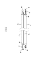
FIG. 1 is a perspective view of a socket in accordance with one embodiment of the invention; -
FIG. 2 is a top view of the socket inFIG. 1 ; -
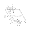
FIG. 3 illustrates that a board is seated in the socket ofFIG. 1 ; -
FIG. 4 is a view similar toFIG. 3 , illustrating that the latches at the ends of the socket are in latched positions; -
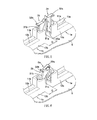
FIG. 5 illustrates that two sockets are arranged end to end on a circuit board with the adjacent latches in the open positions; -
FIG. 6 is a view similar toFIG. 5 , illustrating that the adjacent latches of the two sockets are in the latched positions; -
FIG. 7 is top view of a prior art motherboard; -
FIG. 8 is a perspective view of two prior art sockets with end latches in latched positions; and -
FIG. 9 is a view similar toFIG. 8 , illustrating that the end latches of the prior art sockets are in open positions. - Referring now to
FIGS. 1 and2 , a socket in accordance with one embodiment of the invention includes ahousing 1, afirst latch 2 and asecond latch 3. - The
housing 1 includes afirst side plate 11 and asecond side plate 12. Thefirst side plate 11 andsecond side plates 12 are parallel to each other and co-define anelongated slot 10 therebetween for reception of a board 4 (FIG. 3 ). - As shown in
FIG. 1 , thefirst latch 2 includes afirst axle 20, afirst body 21 and afirst fastening portion 22. Thefirst axle 20 is pivotably coupled to thehousing 1 at one end of theslot 10. Thefirst body 21 has its lower end joined to thefirst axle 20 and the upper end to thefirst fastening portion 22. Moreover, the lateral width of thefirst body 21 of thefirst latch 2 in the direction along the width of thefirst side plate 11 is smaller than that of thefirst axle 20 from the same direction. Thefirst fastening portion 22 is constructed for engagement with one end of theboard 4. In this embodiment, thefirst fastening portion 22 is, but not limited to, a protrusion or a latching projection extending from thefirst body 21 to enhance engagement with theboard 4. -
FIG. 2 is a top view of the socket inFIG. 1 . As can be seen inFIG. 2 , thesecond latch 3 includes asecond axle 30, asecond body 31 and asecond fastening portion 32. Thesecond axle 30 is pivotably coupled to thehousing 1 at the other end of theslot 10. Similar to thefirst body 21, thesecond body 31 has its lower end joined to thesecond axle 30 and the upper end to thesecond fastening portion 32. Moreover, the lateral width of thesecond body 31 of thesecond latch 3 in the direction along the width of thesecond side plate 12 is smaller than that of thesecond axle 30 in the same direction. Thesecond fastening portion 32 is constructed for engagement with the other end of theboard 4. In this embodiment, thesecond fastening portion 32 is, but not limited to, a protrusion or a latching projection extending from thesecond body 31 to enhance engagement with theboard 4. -
FIG. 3 illustrates that theboard 4 is seated in the socket, and thefirst body 21 andsecond body 31 are rotated about the respectivefirst axle 20 andsecond axles 30 to the open positions. Theboard 4 has an edge portion received in theslot 10 of thehousing 1 of the socket. Theboard 4 may be an interface card, an adapter card, a dual inline memory module (DIMM) or other types of circuit board card, or even just a dummy board with no electrical traces printed thereon. In this embodiment, theboard 4 is a dual inline memory module with afirst notch 40 and asecond notch 41 at opposite ends thereof, and the socket is a specialized DIMM socket for theboard 4. Thefirst fastening portion 22 and thesecond fastening portion 32 of the socket are configured to be engaged in thefirst notch 40 and thesecond notch 41 of theboard 4.FIG. 3 illustrates that thefirst fastening portions 22 andsecond fastening portion 32 are detached away from the corresponding 40 and notch 41 of theboard 4 to release theboard 4. - In contrast,
FIG. 4 illustrates that theboard 4 is seated in the socket while thefirst body 21 and thesecond body 31 are rotated to the closed or latched positions. At this time, thefirst fastening portion 22 andsecond fastening portions 32 of the socket are engaged in thefirst notch 40 and thesecond notche 41 of theboard 4 respectively, and therefore theboard 4 is securely seated in the socket and is not allowed to be extracted from the socket. - In particular, since the lateral width of the
first body 21 from thefirst side plate 11 is smaller than that of thefirst axle 20 from thefirst side plate 11 and also the lateral width of thesecond body 31 from thesecond side plate 12 is smaller than that of thesecond axle 30 from thesecond side plate 12, the first and second bodys 21, 31 of the socket are staggered in position. In doing so, two aforementioned sockets can be arranged end to end on a circuit board to save space, as will be discussed later. - In concerned with the injection mould cost, the first and
second latches first latch 2 or thesecond latch 3, rather than two latches so as to keep the cost down further. - In this embodiment, the lateral width of the
first body 21 in the direction along the width of thefirst side plate 11 equals one half of that of thefirst axle 20 in the same direction; and also the lateral width of thesecond body 31 in the direction along the width of thesecond side plate 12 equals one half of that of thesecond axle 30 in the same direction. - With reference to
FIG. 5 , a motherboard in accordance with one embodiment of the invention includes a circuit board 5, a first socket and a second socket. The first and second sockets are similar to the aforementioned socket. Specifically, the first socket includes afirst housing 1a and afirst latch 2a. The second socket includes asecond housing 1b and asecond latch 3b. For clarity, only partial portions of the sockets are depicted inFIG. 5 . - The
first housing 1a of the first socket includes afirst side plate 11a and asecond side plate 12a parallel to thefirst side plate 11a. The first andsecond side plates elongated slot 10a therebetween for reception of a first board (not shown). On the other hand, thefirst latch 2a of the first socket includes afirst axle 20a, afirst body 21a and afirst fastening portion 22a. Thefirst axle 21a is pivotably coupled to thefirst housing 1a at one end of the firstelongated slot 10a. Thefirst body 21a has its lower end joined to thefirst axle 21a and the upper end to thefirst fastening portion 22a. Similar to thefirst fastening portion 22 ofFIG. 1 , thefirst fastening portion 22a is constructed for engagement with the first board. Substantially all of the features on thefirst fastening portion 22 ofFIG. 1 apply to thefirst fastening portion 22a and will not be discussed further herein. In this embodiment, thefirst fastening portion 22a is, but not limited to, a protrusion or a latching projection extending from thefirst body 21a. - The
second housing 1b of the second socket includes athird side plate 11b and afourth side plate 12b parallel to thethird side plate 11b. Thethird side plate 11b and thefourth side plate 12b define a secondelongated slot 10b therebetween for reception of a second board (not shown). On the other hand, thesecond latch 3b of the second socket includes a second axle (not shown, but similar to thesecond axle 30 ofFIG. 2 ), asecond body 31b and asecond fastening portion 32b. Thesecond axle 31b is pivotably coupled to thesecond housing 1b at one end of the secondelongated slot 10b. Thesecond body 31b has its lower end joined to the second axle and the upper end to thesecond fastening portion 32b. Thesecond fastening portion 32b is constructed for engagement with the second board. Substantially all of the features on thesecond fastening portion 32 ofFIG. 1 apply to the second fastening portion 32a and will not be discussed further herein. In this embodiment, the second fastening portion 32a is, but not limited to, a protrusion or a latching projection extending from the second body 31a. - Similarly, the
first latch 2a and second latches 3a may be identical to each other in structure in concerned with the injection mould cost. Preferably, the lateral width of thefirst body 21a of thefirst latch 2a in the direction along the width of thefirst side plate 11a equals one half of the distance between thefirst side plate 11a andsecond side plate 12b. In addition, the lateral width of thesecond body 31b of thesecond latch 3b from thefourth side plate 12b of thesecond housing 1b equals one half of the distance between the third andfourth side plates - It should be noted that the first and second latches are not limited to specific configuration as disclosed above, but may be formed in other types of construction as long as they are staggered. For example, the lateral width of the first body may equal two third of the distance between the first and second side plates and the lateral width of the second body may equal one third of the distance between the third and fourth side plates such that the first and second bodies are staggered and will not be blocked by each other when the first and second latches are pulled to the open positions. Alternatively, the first body may be formed of two branches, and the second body, staggered with respect to the branches of the first body, can pass through the tunnel defined between the two branches of the first body while the first and second latches are pulled to the open positions.
- As shown in
FIG. 5 , thefirst body 21a of the first socket and thesecond body 31b of the second socket are disposed in the latched positions. Specifically, thefirst axle 20a of the first socket is aligned with the second axle of the second socket. Thefirst body 21a of the first socket, proximal to thefirst side plate 11a, is aligned with a space defined by thesecond body 31b and thethird side plate 11b of the second socket. In contrast, thesecond body 31b of the second socket, proximal to thefourth side plate 12b, is aligned with a space defined by thefirst body 21a and thesecond side plate 12a of the first socket. As a result, thefirst body 21a of the first socket and thesecond body 31b of the second socket are staggered and will not be blocked by each other from moving to the open positions, as shown inFIG. 6 . In such a manner, the gap G is quite small in comparison with the interval W inFIGS. 8 or 9 . In other words, the gap betweenfirst housing 1a and thesecond housing 1b can be reduced or even brought down to zero if required, and thereby maximum the space utilization of the circuit board. - It will be appreciated that although a particular embodiment of the invention has been shown and described, modifications may be made. It is intended in the claims to cover such modifications which come within the spirit and scope of the invention.
Claims (10)
- A socket selectively mounting a board therein, comprising:a housing including a first side plate and a second side plate parallel to the first side plate; the first plate and the second side plate together defining an elongated slot therebetween for reception of the board; anda first latch including a first axle, a first body and a first fastening portion; the first axle pivotably coupled to the housing at one end of the slot; the first body having one end joined to the first axle and the other end to the first fastening portion; the first fastening portion constructed for engagement with the board;wherein the lateral width of the first body of the first latch in a direction along the width of the first side plate is smaller than that of the first axle in the direction.
- The socket of claim 1 further comprising a second latch, the second latch including a second axle, a second body and a second fastening portion; the second latch pivotably coupled to the housing at the other end of the slot; the second body having one end joined to the second axle and the other end to the second fastening portion; the second fastening portion constructed for engagement with the board;
wherein the lateral width of the second body of the second latch in the direction is smaller than that of the second axle in the direction. - The socket of claim 1, wherein the first fastening portion of the first latch is a protrusion extending from the first body.
- The socket of claim 2, wherein the first fastening portion of the first latch is a latching projection extending from the first body, and the second fastening portion of the second latch is a protrusion extending from the second body.
- The socket of claim 2, wherein the lateral width of the first body of the first latch in the direction is half of that of the first axle in the direction;
and the lateral width of the second body of the second latch in the direction is half of that of the second axle in the direction. - The socket of claim 5, wherein the first and second latches are identical.
- A motherboard selectively mounting a first board and a second board thereon, comprising:a first socket including a first housing and a first latch; the first housing including a first side plate and a second side plate parallel to the first side plate; the first and second side plates together defining a first elongated slot therebetween for reception of the first board; and the first latch including a first axle, a first body and a first fastening portion; the first axle pivotably coupled to the first housing at one end of the first elongated slot; the first body having one end joined to the first axle and the other end to the first fastening portion; the first fastening portion constructed for engagement with the first board; anda second socket including a second housing and a second latch; the second housing including a third side plate and a fourth side plate parallel to the third side plate; the third and fourth side plates together defining a second elongated slot therebetween for reception of the second board; and the second latch including a second axle, a second body and a second fastening portion; the second axle pivotably coupled to the second housing at one end of the second elongated slot; the second body having one end joined to the second axle and the other end to the second fastening portion; the second fastening portion constructed for engagement with the second board;wherein the first axle of the first socket is aligned with the second axle of the second socket; the first body of the first socket is aligned with a space defined by the second body and the third side plate of the second socket; and the second body of the second socket is aligned with a space defined by the first body and the second side plate of the first socket.
- The motherboard of claim 7, wherein the first fastening portion of the first latch is a protrusion extending from the first body, and the second fastening portion of the second latch is a protrusion extending from the second body.
- The motherboard of claim 7, wherein the lateral width of the first body of the first latch of the first socket in a direction along the width of the first side plate equals half of the distance between the first side plate and the second side plate; and the lateral width of the second body of the second latch of the second socket in the direction equals half of the distance between the third side plate and the fourth side plate.
- The motherboard of claim 9, wherein the first latch of the first socket and the second latch of the second socket are identical.
Priority Applications (1)
| Application Number | Priority Date | Filing Date | Title |
|---|---|---|---|
| EP10189002.8A EP2448070B1 (en) | 2010-10-27 | 2010-10-27 | Socket and motherboard with the same |
Applications Claiming Priority (1)
| Application Number | Priority Date | Filing Date | Title |
|---|---|---|---|
| EP10189002.8A EP2448070B1 (en) | 2010-10-27 | 2010-10-27 | Socket and motherboard with the same |
Publications (2)
| Publication Number | Publication Date |
|---|---|
| EP2448070A1 true EP2448070A1 (en) | 2012-05-02 |
| EP2448070B1 EP2448070B1 (en) | 2016-09-21 |
Family
ID=43281983
Family Applications (1)
| Application Number | Title | Priority Date | Filing Date |
|---|---|---|---|
| EP10189002.8A Not-in-force EP2448070B1 (en) | 2010-10-27 | 2010-10-27 | Socket and motherboard with the same |
Country Status (1)
| Country | Link |
|---|---|
| EP (1) | EP2448070B1 (en) |
Citations (5)
| Publication number | Priority date | Publication date | Assignee | Title |
|---|---|---|---|---|
| EP0975067A1 (en) * | 1998-07-17 | 2000-01-26 | Molex Incorporated | Card edge connector with improved reference terminals |
| US6074232A (en) * | 1998-06-01 | 2000-06-13 | Hon Hai Precision Ind. Co., Ltd. | Board to board electrical connector with releaseable actuator |
| US6290519B1 (en) * | 2000-12-28 | 2001-09-18 | Hon Hai Precision Ind. Co., Ltd. | Ejector for use with a card edge connector |
| WO2005029936A1 (en) * | 2003-09-12 | 2005-03-31 | Molex Incorporated | Memory module connector with release mechanism |
| EP1791224A1 (en) * | 2005-11-28 | 2007-05-30 | Hon Hai Precision Industry Co., Ltd. | Card edge connector |
Family Cites Families (2)
| Publication number | Priority date | Publication date | Assignee | Title |
|---|---|---|---|---|
| JPH0686278U (en) * | 1993-05-27 | 1994-12-13 | 日本航空電子工業株式会社 | Card edge connector |
| JP2006054191A (en) * | 2002-12-17 | 2006-02-23 | Yamaichi Electronics Co Ltd | Socket for semiconductor device |
-
2010
- 2010-10-27 EP EP10189002.8A patent/EP2448070B1/en not_active Not-in-force
Patent Citations (5)
| Publication number | Priority date | Publication date | Assignee | Title |
|---|---|---|---|---|
| US6074232A (en) * | 1998-06-01 | 2000-06-13 | Hon Hai Precision Ind. Co., Ltd. | Board to board electrical connector with releaseable actuator |
| EP0975067A1 (en) * | 1998-07-17 | 2000-01-26 | Molex Incorporated | Card edge connector with improved reference terminals |
| US6290519B1 (en) * | 2000-12-28 | 2001-09-18 | Hon Hai Precision Ind. Co., Ltd. | Ejector for use with a card edge connector |
| WO2005029936A1 (en) * | 2003-09-12 | 2005-03-31 | Molex Incorporated | Memory module connector with release mechanism |
| EP1791224A1 (en) * | 2005-11-28 | 2007-05-30 | Hon Hai Precision Industry Co., Ltd. | Card edge connector |
Also Published As
| Publication number | Publication date |
|---|---|
| EP2448070B1 (en) | 2016-09-21 |
Similar Documents
| Publication | Publication Date | Title |
|---|---|---|
| US8657612B2 (en) | Socket and motherboard with the same | |
| US8277235B2 (en) | Socket and motherboard with the same | |
| US8597056B2 (en) | Card edge connector | |
| US8092262B1 (en) | Eye-of-the needle pin of an electrical contact | |
| US8231411B1 (en) | Card edge connector | |
| TWI458181B (en) | Socket connector with power blade | |
| CN102255201B (en) | Between adjacent signal contact, there is the socket connector of ground shield | |
| US7540743B2 (en) | Memory module, memory module socket and mainboard using same | |
| CN102176557B (en) | High density bottom plate connector | |
| TWI437764B (en) | Electrical connector assembly with shorting contacts | |
| US8634199B2 (en) | Computer mini-card connection assembly | |
| US20120225588A1 (en) | Card edge connector | |
| US20120190219A1 (en) | Motherboard and memory connector thereof | |
| US20100317234A1 (en) | Card edge connector with improved soldering portions of terminals | |
| US9172165B1 (en) | Memory module connector assembly | |
| US20140065881A1 (en) | Multi-socket memory module t-connector | |
| US20200083623A1 (en) | Dual in-line memory modules and connectors for increased system performance | |
| CN103166048A (en) | Slot device and main board with slot device installed | |
| CN103425199B (en) | Memory module and electric connector | |
| US8419457B2 (en) | Anti-electromagnetic interference electrical connector and terminal assembly thereof | |
| US7264489B2 (en) | Dual connector assembly with pivoting keep-out member | |
| US8113850B2 (en) | Computer | |
| US8979561B2 (en) | Interleaving ejector latches enabling a reduced end-to-end spacing between memory module connectors | |
| EP2448070B1 (en) | Socket and motherboard with the same | |
| US9039456B2 (en) | Electrical connector with fastening elements |
Legal Events
| Date | Code | Title | Description |
|---|---|---|---|
| PUAI | Public reference made under article 153(3) epc to a published international application that has entered the european phase |
Free format text: ORIGINAL CODE: 0009012 |
|
| AK | Designated contracting states |
Kind code of ref document: A1 Designated state(s): AL AT BE BG CH CY CZ DE DK EE ES FI FR GB GR HR HU IE IS IT LI LT LU LV MC MK MT NL NO PL PT RO RS SE SI SK SM TR |
|
| AX | Request for extension of the european patent |
Extension state: BA ME |
|
| 17P | Request for examination filed |
Effective date: 20121031 |
|
| 17Q | First examination report despatched |
Effective date: 20130408 |
|
| RAP1 | Party data changed (applicant data changed or rights of an application transferred) |
Owner name: GIGA-BYTE TECHNOLOGY CO., LTD. |
|
| GRAP | Despatch of communication of intention to grant a patent |
Free format text: ORIGINAL CODE: EPIDOSNIGR1 |
|
| INTG | Intention to grant announced |
Effective date: 20160404 |
|
| GRAS | Grant fee paid |
Free format text: ORIGINAL CODE: EPIDOSNIGR3 |
|
| GRAA | (expected) grant |
Free format text: ORIGINAL CODE: 0009210 |
|
| REG | Reference to a national code |
Ref country code: FR Ref legal event code: PLFP Year of fee payment: 7 |
|
| AK | Designated contracting states |
Kind code of ref document: B1 Designated state(s): AL AT BE BG CH CY CZ DE DK EE ES FI FR GB GR HR HU IE IS IT LI LT LU LV MC MK MT NL NO PL PT RO RS SE SI SK SM TR |
|
| REG | Reference to a national code |
Ref country code: GB Ref legal event code: FG4D |
|
| REG | Reference to a national code |
Ref country code: CH Ref legal event code: EP |
|
| REG | Reference to a national code |
Ref country code: AT Ref legal event code: REF Ref document number: 831716 Country of ref document: AT Kind code of ref document: T Effective date: 20161015 |
|
| REG | Reference to a national code |
Ref country code: IE Ref legal event code: FG4D |
|
| REG | Reference to a national code |
Ref country code: DE Ref legal event code: R096 Ref document number: 602010036541 Country of ref document: DE |
|
| REG | Reference to a national code |
Ref country code: LT Ref legal event code: MG4D Ref country code: NL Ref legal event code: MP Effective date: 20160921 |
|
| PG25 | Lapsed in a contracting state [announced via postgrant information from national office to epo] |
Ref country code: FI Free format text: LAPSE BECAUSE OF FAILURE TO SUBMIT A TRANSLATION OF THE DESCRIPTION OR TO PAY THE FEE WITHIN THE PRESCRIBED TIME-LIMIT Effective date: 20160921 Ref country code: NO Free format text: LAPSE BECAUSE OF FAILURE TO SUBMIT A TRANSLATION OF THE DESCRIPTION OR TO PAY THE FEE WITHIN THE PRESCRIBED TIME-LIMIT Effective date: 20161221 Ref country code: LT Free format text: LAPSE BECAUSE OF FAILURE TO SUBMIT A TRANSLATION OF THE DESCRIPTION OR TO PAY THE FEE WITHIN THE PRESCRIBED TIME-LIMIT Effective date: 20160921 Ref country code: RS Free format text: LAPSE BECAUSE OF FAILURE TO SUBMIT A TRANSLATION OF THE DESCRIPTION OR TO PAY THE FEE WITHIN THE PRESCRIBED TIME-LIMIT Effective date: 20160921 |
|
| REG | Reference to a national code |
Ref country code: AT Ref legal event code: MK05 Ref document number: 831716 Country of ref document: AT Kind code of ref document: T Effective date: 20160921 |
|
| PG25 | Lapsed in a contracting state [announced via postgrant information from national office to epo] |
Ref country code: LV Free format text: LAPSE BECAUSE OF FAILURE TO SUBMIT A TRANSLATION OF THE DESCRIPTION OR TO PAY THE FEE WITHIN THE PRESCRIBED TIME-LIMIT Effective date: 20160921 Ref country code: GR Free format text: LAPSE BECAUSE OF FAILURE TO SUBMIT A TRANSLATION OF THE DESCRIPTION OR TO PAY THE FEE WITHIN THE PRESCRIBED TIME-LIMIT Effective date: 20161222 Ref country code: NL Free format text: LAPSE BECAUSE OF FAILURE TO SUBMIT A TRANSLATION OF THE DESCRIPTION OR TO PAY THE FEE WITHIN THE PRESCRIBED TIME-LIMIT Effective date: 20160921 Ref country code: SE Free format text: LAPSE BECAUSE OF FAILURE TO SUBMIT A TRANSLATION OF THE DESCRIPTION OR TO PAY THE FEE WITHIN THE PRESCRIBED TIME-LIMIT Effective date: 20160921 Ref country code: BE Free format text: LAPSE BECAUSE OF NON-PAYMENT OF DUE FEES Effective date: 20161031 |
|
| PG25 | Lapsed in a contracting state [announced via postgrant information from national office to epo] |
Ref country code: EE Free format text: LAPSE BECAUSE OF FAILURE TO SUBMIT A TRANSLATION OF THE DESCRIPTION OR TO PAY THE FEE WITHIN THE PRESCRIBED TIME-LIMIT Effective date: 20160921 Ref country code: RO Free format text: LAPSE BECAUSE OF FAILURE TO SUBMIT A TRANSLATION OF THE DESCRIPTION OR TO PAY THE FEE WITHIN THE PRESCRIBED TIME-LIMIT Effective date: 20160921 |
|
| PG25 | Lapsed in a contracting state [announced via postgrant information from national office to epo] |
Ref country code: BG Free format text: LAPSE BECAUSE OF FAILURE TO SUBMIT A TRANSLATION OF THE DESCRIPTION OR TO PAY THE FEE WITHIN THE PRESCRIBED TIME-LIMIT Effective date: 20161221 Ref country code: BE Free format text: LAPSE BECAUSE OF FAILURE TO SUBMIT A TRANSLATION OF THE DESCRIPTION OR TO PAY THE FEE WITHIN THE PRESCRIBED TIME-LIMIT Effective date: 20160921 Ref country code: SK Free format text: LAPSE BECAUSE OF FAILURE TO SUBMIT A TRANSLATION OF THE DESCRIPTION OR TO PAY THE FEE WITHIN THE PRESCRIBED TIME-LIMIT Effective date: 20160921 Ref country code: SM Free format text: LAPSE BECAUSE OF FAILURE TO SUBMIT A TRANSLATION OF THE DESCRIPTION OR TO PAY THE FEE WITHIN THE PRESCRIBED TIME-LIMIT Effective date: 20160921 Ref country code: PT Free format text: LAPSE BECAUSE OF FAILURE TO SUBMIT A TRANSLATION OF THE DESCRIPTION OR TO PAY THE FEE WITHIN THE PRESCRIBED TIME-LIMIT Effective date: 20170123 Ref country code: ES Free format text: LAPSE BECAUSE OF FAILURE TO SUBMIT A TRANSLATION OF THE DESCRIPTION OR TO PAY THE FEE WITHIN THE PRESCRIBED TIME-LIMIT Effective date: 20160921 Ref country code: AT Free format text: LAPSE BECAUSE OF FAILURE TO SUBMIT A TRANSLATION OF THE DESCRIPTION OR TO PAY THE FEE WITHIN THE PRESCRIBED TIME-LIMIT Effective date: 20160921 Ref country code: IS Free format text: LAPSE BECAUSE OF FAILURE TO SUBMIT A TRANSLATION OF THE DESCRIPTION OR TO PAY THE FEE WITHIN THE PRESCRIBED TIME-LIMIT Effective date: 20170121 Ref country code: PL Free format text: LAPSE BECAUSE OF FAILURE TO SUBMIT A TRANSLATION OF THE DESCRIPTION OR TO PAY THE FEE WITHIN THE PRESCRIBED TIME-LIMIT Effective date: 20160921 Ref country code: CZ Free format text: LAPSE BECAUSE OF FAILURE TO SUBMIT A TRANSLATION OF THE DESCRIPTION OR TO PAY THE FEE WITHIN THE PRESCRIBED TIME-LIMIT Effective date: 20160921 |
|
| REG | Reference to a national code |
Ref country code: CH Ref legal event code: PL |
|
| REG | Reference to a national code |
Ref country code: DE Ref legal event code: R097 Ref document number: 602010036541 Country of ref document: DE |
|
| PG25 | Lapsed in a contracting state [announced via postgrant information from national office to epo] |
Ref country code: IT Free format text: LAPSE BECAUSE OF FAILURE TO SUBMIT A TRANSLATION OF THE DESCRIPTION OR TO PAY THE FEE WITHIN THE PRESCRIBED TIME-LIMIT Effective date: 20160921 |
|
| REG | Reference to a national code |
Ref country code: IE Ref legal event code: MM4A |
|
| PLBE | No opposition filed within time limit |
Free format text: ORIGINAL CODE: 0009261 |
|
| STAA | Information on the status of an ep patent application or granted ep patent |
Free format text: STATUS: NO OPPOSITION FILED WITHIN TIME LIMIT |
|
| PG25 | Lapsed in a contracting state [announced via postgrant information from national office to epo] |
Ref country code: DK Free format text: LAPSE BECAUSE OF FAILURE TO SUBMIT A TRANSLATION OF THE DESCRIPTION OR TO PAY THE FEE WITHIN THE PRESCRIBED TIME-LIMIT Effective date: 20160921 Ref country code: LI Free format text: LAPSE BECAUSE OF NON-PAYMENT OF DUE FEES Effective date: 20161031 Ref country code: CH Free format text: LAPSE BECAUSE OF NON-PAYMENT OF DUE FEES Effective date: 20161031 |
|
| 26N | No opposition filed |
Effective date: 20170622 |
|
| PG25 | Lapsed in a contracting state [announced via postgrant information from national office to epo] |
Ref country code: LU Free format text: LAPSE BECAUSE OF NON-PAYMENT OF DUE FEES Effective date: 20161027 |
|
| REG | Reference to a national code |
Ref country code: FR Ref legal event code: PLFP Year of fee payment: 8 |
|
| PG25 | Lapsed in a contracting state [announced via postgrant information from national office to epo] |
Ref country code: SI Free format text: LAPSE BECAUSE OF FAILURE TO SUBMIT A TRANSLATION OF THE DESCRIPTION OR TO PAY THE FEE WITHIN THE PRESCRIBED TIME-LIMIT Effective date: 20160921 Ref country code: IE Free format text: LAPSE BECAUSE OF NON-PAYMENT OF DUE FEES Effective date: 20161027 |
|
| PG25 | Lapsed in a contracting state [announced via postgrant information from national office to epo] |
Ref country code: CY Free format text: LAPSE BECAUSE OF FAILURE TO SUBMIT A TRANSLATION OF THE DESCRIPTION OR TO PAY THE FEE WITHIN THE PRESCRIBED TIME-LIMIT Effective date: 20160921 Ref country code: HU Free format text: LAPSE BECAUSE OF FAILURE TO SUBMIT A TRANSLATION OF THE DESCRIPTION OR TO PAY THE FEE WITHIN THE PRESCRIBED TIME-LIMIT; INVALID AB INITIO Effective date: 20101027 |
|
| PG25 | Lapsed in a contracting state [announced via postgrant information from national office to epo] |
Ref country code: TR Free format text: LAPSE BECAUSE OF FAILURE TO SUBMIT A TRANSLATION OF THE DESCRIPTION OR TO PAY THE FEE WITHIN THE PRESCRIBED TIME-LIMIT Effective date: 20160921 Ref country code: MK Free format text: LAPSE BECAUSE OF FAILURE TO SUBMIT A TRANSLATION OF THE DESCRIPTION OR TO PAY THE FEE WITHIN THE PRESCRIBED TIME-LIMIT Effective date: 20160921 Ref country code: MT Free format text: LAPSE BECAUSE OF NON-PAYMENT OF DUE FEES Effective date: 20161031 Ref country code: HR Free format text: LAPSE BECAUSE OF FAILURE TO SUBMIT A TRANSLATION OF THE DESCRIPTION OR TO PAY THE FEE WITHIN THE PRESCRIBED TIME-LIMIT Effective date: 20160921 Ref country code: MC Free format text: LAPSE BECAUSE OF FAILURE TO SUBMIT A TRANSLATION OF THE DESCRIPTION OR TO PAY THE FEE WITHIN THE PRESCRIBED TIME-LIMIT Effective date: 20160921 |
|
| REG | Reference to a national code |
Ref country code: FR Ref legal event code: PLFP Year of fee payment: 9 |
|
| PG25 | Lapsed in a contracting state [announced via postgrant information from national office to epo] |
Ref country code: AL Free format text: LAPSE BECAUSE OF FAILURE TO SUBMIT A TRANSLATION OF THE DESCRIPTION OR TO PAY THE FEE WITHIN THE PRESCRIBED TIME-LIMIT Effective date: 20160921 |
|
| PGFP | Annual fee paid to national office [announced via postgrant information from national office to epo] |
Ref country code: FR Payment date: 20200914 Year of fee payment: 11 |
|
| PGFP | Annual fee paid to national office [announced via postgrant information from national office to epo] |
Ref country code: DE Payment date: 20201013 Year of fee payment: 11 Ref country code: GB Payment date: 20201014 Year of fee payment: 11 |
|
| REG | Reference to a national code |
Ref country code: DE Ref legal event code: R119 Ref document number: 602010036541 Country of ref document: DE |
|
| GBPC | Gb: european patent ceased through non-payment of renewal fee |
Effective date: 20211027 |
|
| PG25 | Lapsed in a contracting state [announced via postgrant information from national office to epo] |
Ref country code: GB Free format text: LAPSE BECAUSE OF NON-PAYMENT OF DUE FEES Effective date: 20211027 Ref country code: DE Free format text: LAPSE BECAUSE OF NON-PAYMENT OF DUE FEES Effective date: 20220503 |
|
| PG25 | Lapsed in a contracting state [announced via postgrant information from national office to epo] |
Ref country code: FR Free format text: LAPSE BECAUSE OF NON-PAYMENT OF DUE FEES Effective date: 20211031 |