EP2445113A1 - Reconfigurable wide-band radio receiver with positive feed-back translational loop - Google Patents
Reconfigurable wide-band radio receiver with positive feed-back translational loop Download PDFInfo
- Publication number
- EP2445113A1 EP2445113A1 EP10194629A EP10194629A EP2445113A1 EP 2445113 A1 EP2445113 A1 EP 2445113A1 EP 10194629 A EP10194629 A EP 10194629A EP 10194629 A EP10194629 A EP 10194629A EP 2445113 A1 EP2445113 A1 EP 2445113A1
- Authority
- EP
- European Patent Office
- Prior art keywords
- input
- signal
- output
- direct path
- block
- Prior art date
- Legal status (The legal status is an assumption and is not a legal conclusion. Google has not performed a legal analysis and makes no representation as to the accuracy of the status listed.)
- Granted
Links
- 238000001914 filtration Methods 0.000 claims abstract description 14
- 238000000034 method Methods 0.000 claims description 8
- 230000014509 gene expression Effects 0.000 description 14
- 230000006870 function Effects 0.000 description 9
- 238000010897 surface acoustic wave method Methods 0.000 description 5
- 238000004590 computer program Methods 0.000 description 4
- 238000010586 diagram Methods 0.000 description 4
- 238000013459 approach Methods 0.000 description 3
- 239000003990 capacitor Substances 0.000 description 3
- 230000010365 information processing Effects 0.000 description 3
- 230000008901 benefit Effects 0.000 description 2
- 238000006243 chemical reaction Methods 0.000 description 2
- 230000007423 decrease Effects 0.000 description 2
- 238000013461 design Methods 0.000 description 2
- 238000012986 modification Methods 0.000 description 2
- 230000004048 modification Effects 0.000 description 2
- 238000004088 simulation Methods 0.000 description 2
- 239000000872 buffer Substances 0.000 description 1
- 230000001413 cellular effect Effects 0.000 description 1
- 230000000295 complement effect Effects 0.000 description 1
- 238000010295 mobile communication Methods 0.000 description 1
- 238000012545 processing Methods 0.000 description 1
- 230000035945 sensitivity Effects 0.000 description 1
- 238000012546 transfer Methods 0.000 description 1
Images


Classifications
-
- H—ELECTRICITY
- H04—ELECTRIC COMMUNICATION TECHNIQUE
- H04B—TRANSMISSION
- H04B1/00—Details of transmission systems, not covered by a single one of groups H04B3/00 - H04B13/00; Details of transmission systems not characterised by the medium used for transmission
- H04B1/06—Receivers
- H04B1/16—Circuits
-
- H—ELECTRICITY
- H04—ELECTRIC COMMUNICATION TECHNIQUE
- H04B—TRANSMISSION
- H04B1/00—Details of transmission systems, not covered by a single one of groups H04B3/00 - H04B13/00; Details of transmission systems not characterised by the medium used for transmission
- H04B1/005—Details of transmission systems, not covered by a single one of groups H04B3/00 - H04B13/00; Details of transmission systems not characterised by the medium used for transmission adapting radio receivers, transmitters andtransceivers for operation on two or more bands, i.e. frequency ranges
- H04B1/0053—Details of transmission systems, not covered by a single one of groups H04B3/00 - H04B13/00; Details of transmission systems not characterised by the medium used for transmission adapting radio receivers, transmitters andtransceivers for operation on two or more bands, i.e. frequency ranges with common antenna for more than one band
Definitions
- the present invention generally relates to signal processing for the reception of radio signals, especially by wide-band receivers.
- radio-frequency receiver e.g., Software Defined Radio receiver
- cellular phones and other mobile communication devices e.g., cellular phones and other mobile communication devices.
- SDR Software Defined Radio
- SDR aims the capability of supporting multiple radio standards and bands.
- SDR are adapted to receive radio frequency signals in a plurality of frequency ranges.
- LNA Low Noise Amplifier
- SAW Surface Acoustic Wave
- SAW filters cancels all benefits of a wide-band receiver design. Indeed, the LNA can no longer be shared among different frequency ranges because of the SAW filter included between the LNA and the antenna, which filters the received signal in a unique narrow band and which is not reconfigurable. To obtain a wide-band receiver, it is then necessary to have such a receiver, or at least a part of it, for each of the radio frequency ranges, instead of having a unique receiver for a plurality of frequency ranges. Furthermore, SAW filters add extra components, board area and degrade the receiver sensitivity by 2 to 3dB.
- a first aspect of the present invention relates to a device comprising a direct path block with an input and an output, and a feedback block with an input and an output, the input of the direct block path being adapted to receive a multi-channel input signal with a given frequency range and the output of the direct block path being adapted to output an output signal with a base band frequency range, the output of the direct path block being coupled to the input of the feedback block and the input of the direct path block being coupled to the output of the feedback block, wherein:
- the first transposing unit and the second transposing unit comprise a first mixer and a second mixer, respectively, and a common oscillator coupled to the first mixer and to the second mixer.
- the oscillator delivers a signal at a frequency, which depends dynamically on the given frequency range of the input signal.
- the direct path block further comprises an amplifying unit adapted to amplify the input signal at the input of the direct path block.
- the filtering unit is a low-pass filter and the transposed signal is positively fed back at the input of the direct path block.
- the feedback block further comprises a feedback amplifier adapted to amplify the transposed signal and to feed back the amplified signal at the input of the direct path block.
- parameters of the feedback block can also be configured so that an input impedance defined by the ratio of a voltage at the input of the device on an input current at the input of the device is set to given value.
- the device is a wide band receiver.
- Another object of the invention relates to a method being implemented by a device comprising a direct path block with an input and an output, and a feedback block with an input and an output, being adapted to receive a multi-channel input signal with a given frequency range and being adapted to output an output signal with a base band frequency range, the output of the direct path block being coupled to the input of the feedback block and the input of the direct path block being coupled to the output of the feedback block, the method comprising :
- the filtering of the transposed signal is a low-pass filtering and the feeding back is positive.
- parameters of the feedback block can be configured so that an input impedance defined by the ratio of a voltage at the input of the device on an input current at the input of the device, is set to a given value.
- Still another object of the invention concerns a system comprising a device according to one embodiment of the invention, a receiving unit adapted to receive an input signal with a given frequency range and adapted to provide the device with the input signal, and an output filtering unit adapted to filter the output signal at the output of the device.
- the device 1 represented here can be a receiver that comprises, in one embodiment, a direct path block with an input being coupled to an input of the receiver 1, and an output coupled to an output of the receiver 1, comprising a first amplifier 2, a mixer 4 and a second amplifier 6, and a feedback block, with an input and an output, comprising a feedback filter 3, a feedback mixer 5 and a feedback amplifier 7.
- the output of the direct path block can be coupled to the input of the feedback block and the input of the direct path block can be coupled to the output of the feedback block.
- Receiver 1 input can be coupled to an antenna 8 adapted to receive and deliver to receiver 1 radio frequency signals with a given frequency range among a plurality of frequency ranges.
- Receiver 1 can be adapted to provide an output signal filtered and transposed to a base band frequency range to be further filtered by a filter 9 and transmitted to an analogical-to-digital converter 10 in order to be digitally processed by a system comprising the receiver 1 for example.
- first amplifier 2 is a Low Noise Amplifier adapted to amplify the input signal that is received from the antenna 8.
- Amplifier 2 can be adapted to receive an input signal obtained on the basis of a signal provided by the antenna 8 and a signal provided by the feedback amplifier 7. In the example represented on figure 2 , both signals can be summed or subtracted to obtain input signal of amplifier 2.
- Low Noise Amplifier 2 can also be configured to provide an amplified signal that is transmitted to the mixer 4.
- first mixer 4 is adapted to receive the amplified signal from amplifier 2 and a signal with frequency f LO , which is provided by a common oscillator 11.
- the frequency of the signal delivered by the common oscillator 11 can be configurable and thus adapted to the frequency range of the input signal.
- a table can associate a frequency f LO to each of the frequency ranges that can be received by receiver 1 and can be used to adapt frequency f LO to the received signal.
- the mixer 4 is adapted to generate a mixed signal obtained by translating the amplified signal around frequency f LO , in a base band frequency range (lower frequencies) in order to be further processed.
- the receiver is adapted to process signals with a plurality of frequency ranges insofar as the common oscillator 11 can be configurable to transpose the received signal to the base band frequency range.
- Second amplifier 6 is configured to output a second amplified signal, where the part of the signal in the base band frequencies is amplified, in order to be transmitted to the filter 9 and to an input of the feedback filter 3.
- Feedback filter 3 is adapted to output a filtered signal based on the received amplified signal and to transmit the filtered signal to the feedback mixer 5.
- feedback filter 3 can be a low-pass filter or a high-pass filter.
- Feedback mixer 5 can be configured to receive the filtered signal and also a signal outputted an oscillator. On the example represented here, the common oscillator 11 outputs signals with frequency f LO to be mixed by both mixer 4 and feedback mixer 5.
- Feedback mixer 4 is configured to output a second mixed signal based on the filtered signal and the signal with frequency f LO , which enables to transpose the base band signal to the same frequency range as the given frequency range of the input signal outputted by antenna 8 for example.
- the mixed signal is transmitted to the feedback amplifier 7, which can be for example a trans-conductance amplifier adapted to output a signal which is added or subtracted to the signal provided by antenna 8 and transmitted to the first amplifier 2.
- receiver 1 will be better understood in view of Figure 2 representing a simplified view of the receiver 1 according to one embodiment of the invention.
- Receiver 1 is modelled by a circuit 20.
- Amplifier 2 input impedance is represented in this embodiment by a component 24 of impedance Z LNA and coupled to the ground.
- Antenna 8 is modelled by a voltage source 21 with series impedance Z ANT being a ratio of a voltage V ant , between voltage source 21 input and the ground, on an intensity i in running through the voltage source 21.
- G LNA is the voltage gain of the first amplifier 2
- G mix is the voltage gain of the mixer 4,
- G amp is the voltage gain of the second amplifier 6.
- V BB is the voltage between the output of the direct path block and the ground
- G fil is the voltage gain of the feedback filter 3, which depends on the frequency of the signal received from the second amplifier 6,
- G mix is the voltage gain of the feedback mixer 6, which, in this example, equals the voltage gain of the mixer 4.
- g OTA is the trans-conductance of feedback amplifier 7, which is defined by the ratio of the intensity i FB on the voltage across the feedback amplifier 7.
- Both the path through the direct path block and the path through the feedback block go through a mixer stage (respectively implemented by mixer 4 and by feedback mixer 5) with identical frequency f LO .
- the common mixer stage can be implemented as quadrature direct conversion architecture.
- Amplifier 2 being defined, and thus impedance Z LNA being fixed, receiver 1 can be designed in such a way that input impedance Z IN matches antenna impedance Z ANT only in the frequency band of a desired channel, that is, in the frequency range of the input signal received from antenna 8. Signals that are out of the given frequency range or desired range, also called out-of-band signals, are then filtered on the input of the amplifier 2 due to the impedance mismatch.
- the amplified signal provided by feedback amplifier 7 is subtracted from the signal provided by antenna 8, to cancel signals that are out of the frequency range of the given signal. Different results can be obtained, depending on the type of feedback filter 3 that is used.
- feedback filter 3 is a first order low-pass filter implemented for example with a resistor of value R and a capacitor of capacitance C, defined by a function L Lp (f), and a function L BP (f) which is the mathematical expression of a first order low-pass filter translated around F LO :
- fc 1 2 ⁇ ⁇ RC is the cut off frequency of the filter.
- feedback filter 3 is a first order high pass filter implemented, for example, with a resistor of value R and a capacitor of capacitance C defined by a function H HP (f) and a function H BP (f) which is the mathematical expression of a first order high-pass filter translated around F LO :
- fc 1 2 ⁇ ⁇ RC is the cut-off frequency of the filter.
- FIG. 3 there is shown a graph illustrating simulated input impedance in the receiver 1 for a low-pass filter and a high-pass filter according to the examples previously introduced, versus frequency.
- a matching between input impedances Z IN2 and Z IN1 and antenna impedance Z ANT is made in both cases in a band around frequency f LO .
- input impedance Z IN1 increases when frequency moves away from f LO , thus enabling to reduce the gain for out-of-band signals.
- input impedance Z IN2 decreases when frequency moves away from f LO .
- the amplified signal provided by feedback amplifier 7 is added to the signal provided by antenna 8.
- feedback filter 3 is a first order low-pass filter implemented for example with a resistor of value R and a capacitor of capacitance C, defined by a function L LP (f), and a function L BP (f) which is the mathematical expression of a first order low-pass filter translated around F LO :
- fc 1 2 ⁇ ⁇ RC is the cut-off frequency of the filter.
- Impedance Z LNA can be chosen smaller than Z ANT to reject ou-of-band signals. By increasing the difference between these impedances, the attenuation of the ou-of-band signals is improved.
- dB decibels
- a matching between input impedance Z IN3 and antenna impedance Z ANT is obtained for a feedback low-pass filter in a narrow band around f LO :
- Z IN ⁇ 3 f LO Z LNA 1 -
- Z LNA K Z ANT
- receiver 1 attenuates the signals that are out of the given frequency range of the input signal (also called out-of-band signals).
- the advantage of the positive feedback is the attenuation of every signals by default if impedance Z LNA is smaller than impedance Z ANT .
- the positive feedback allows matching the device with the antenna impedance Z ANT only in the band defined by the low-pass filter of the feedback block. Then, bandwidth loop does not limit the performance of the system because the impedance is only modified for frequency around the signal and the out-of-band signals are filtered as the loop does not work for higher frequency.
- negative feedback HP Filter
- feedback block must work at higher frequency than all out-of-band interferers.
- FIG. 7 a diagram representing input impedance versus frequency for the different values K1, K2 and K3, respectively represented by seventh curve 71, eighth curve 72 and ninth curve 73, for receiver 1 with positive feedback, can be considered.
- K2 for which the architecture of receiver 1 is stable, a strong output signal is fed to the input of receiver 1.
- Impedance Z IN becomes larger than Z ANT and the impedance matching of the device is not achieved.
- Parameters of receiver 1 and in particular of feedback block can be determined so that input impedance Z IN is set to impedance value Z ANT .
- positive feedback in a receiver enables to improve radio frequency filtering attenuation and selectivity for out-of-band signals, when parameters of the feedback block are adjusted depending on the initial value of impedance Z LNA , which is constrained by Low Noise Amplifier 2 design trade off, and on stability considerations.
- the attenuation depends on the value between impedance Z ANT and Z LNA .
- the Z LNA should be lower as possible.
- Selectivity can depend on the cut-off frequency f C , which can be, joined with frequency f LO , configurable for multi-standard and multi-band applications. With realistic values for the various parameters, an attenuation of out-of-band signals of up to -19dB can be obtained.
- receiver 1 with positive feedback is modelled to illustrate the different sources of noise, respectively input noise X s , direct path noise X 1 at the input of direct path block 81, feedback noise X 2 at the input of feedback block 81, and output noise X o at the output of receiver 1.
- X 0 2 A 1 - AB 2 ⁇ X ⁇ s 2 + A 1 - AB 2 ⁇ X 1 2 + AB 1 - AB 2 ⁇ X 2 2 with A being the voltage gain associated to direct path block 81, and B being the voltage gain associated to feedback block 82.
- Feedback block 82 increases the noise in the given frequency range of the received signal (in-band) due to noisy output signal brought to the input of receiver 1.
- gain A can be large.
- gain B will be chosen small, preferably smaller than 1, to decrease the noise and ensure stability.
- the dominant noise contributor will be the direct path block 81, and in particular Low Noise Amplifier 2 and noise impact of the invention can be made small.
- the global noise of the system can be assimilated to the direct path noise X 1 .
- the present invention can also be embedded in a computer program product, which comprises all the features enabling the implementation of the methods described herein, and which, when loaded in an information processing system, causes the information processing system.
- Computer program means or computer program in the present context mean any expression, in any language, code or notation, of a set of instructions intended to cause a system having an information processing capability to perform a particular function either directly or after either or both of the following a) conversion to another language.
- Such a computer program can be stored on a computer or machine readable medium allowing data, instructions, messages or message packets, and other machine readable information to be read from the medium.
- the computer or machine readable medium may include non-volatile memory, such as ROM, Flash memory, Disk drive memory, CD-ROM, and other permanent storage.
- a computer or machine readable medium may include, for example, volatile storage such as RAM, buffers, cache memory, and network circuits.
- the computer or machine readable medium may comprise computer or machine readable information in a transitory state medium such as a network link and/or a network interface, including a wired network or a wireless network, that allow a device to read such computer or machine readable information.
Landscapes
- Engineering & Computer Science (AREA)
- Computer Networks & Wireless Communication (AREA)
- Signal Processing (AREA)
- Circuits Of Receivers In General (AREA)
Abstract
Description
- The present invention generally relates to signal processing for the reception of radio signals, especially by wide-band receivers.
- It finds applications, in particular, in radio-frequency receiver, e.g., Software Defined Radio receiver, in cellular phones and other mobile communication devices.
- The approaches described in this section could be pursued, but are not necessarily approaches that have been previously conceived or pursued. Therefore, unless otherwise indicated herein, the approaches described in this section are not prior art to the claims in this application and are not admitted to be prior art by inclusion in this section.
- Software Defined Radio (SDR) aims the capability of supporting multiple radio standards and bands. For example, SDR are adapted to receive radio frequency signals in a plurality of frequency ranges. To this end, they are usually built with a wide-band Low Noise Amplifier (LNA) followed by a configurable baseband filter, and an analogical-to-digital converter. Nevertheless, constraints are very high and Surface Acoustic Wave (SAW) filters are usually inserted between the antenna input and the receiver input to attenuate interferers in the received signal.
- However, using SAW filters cancels all benefits of a wide-band receiver design. Indeed, the LNA can no longer be shared among different frequency ranges because of the SAW filter included between the LNA and the antenna, which filters the received signal in a unique narrow band and which is not reconfigurable. To obtain a wide-band receiver, it is then necessary to have such a receiver, or at least a part of it, for each of the radio frequency ranges, instead of having a unique receiver for a plurality of frequency ranges. Furthermore, SAW filters add extra components, board area and degrade the receiver sensitivity by 2 to 3dB.
- To address these needs, a first aspect of the present invention relates to a device comprising a direct path block with an input and an output, and a feedback block with an input and an output, the input of the direct block path being adapted to receive a multi-channel input signal with a given frequency range and the output of the direct block path being adapted to output an output signal with a base band frequency range, the output of the direct path block being coupled to the input of the feedback block and the input of the direct path block being coupled to the output of the feedback block, wherein:
- the direct path block comprises a first transposing unit adapted to transpose the input signal to the base band frequency range,
- the feedback block comprises a filtering unit adapted to filter the transposed signal at the output of the direct path block, a second transposing unit adapted to transpose the filtered signal to the given frequency range and to feed back the transposed signal at the input of the direct path block, and
- the first transposing unit and the second transposing unit are reconfigurable in function of the given frequency range of the input signal.
- In one embodiment of the invention, the first transposing unit and the second transposing unit comprise a first mixer and a second mixer, respectively, and a common oscillator coupled to the first mixer and to the second mixer.
- In another embodiment of the invention, the oscillator delivers a signal at a frequency, which depends dynamically on the given frequency range of the input signal.
- In another embodiment of the invention, the direct path block further comprises an amplifying unit adapted to amplify the input signal at the input of the direct path block.
- In still another embodiment of the invention, the filtering unit is a low-pass filter and the transposed signal is positively fed back at the input of the direct path block.
- In still another embodiment of the invention, the feedback block further comprises a feedback amplifier adapted to amplify the transposed signal and to feed back the amplified signal at the input of the direct path block.
- In another embodiment of the invention, parameters of the feedback block can also be configured so that an input impedance defined by the ratio of a voltage at the input of the device on an input current at the input of the device is set to given value.
- In another embodiment of the invention, the device is a wide band receiver.
- Another objet of the invention relates to a method being implemented by a device comprising a direct path block with an input and an output, and a feedback block with an input and an output, being adapted to receive a multi-channel input signal with a given frequency range and being adapted to output an output signal with a base band frequency range, the output of the direct path block being coupled to the input of the feedback block and the input of the direct path block being coupled to the output of the feedback block, the method comprising :
- receiving an input signal with a given frequency range at the input of the direct path block ;
- transposing the input signal to the base band frequency range at the input of the feedback block;
- filtering the transposed signal;
- transposing the filtered signal to the given radio frequency range; and
- feeding back the transposed signal at the input of the direct path block;
- In one embodiment, the filtering of the transposed signal is a low-pass filtering and the feeding back is positive.
- In complement, parameters of the feedback block can be configured so that an input impedance defined by the ratio of a voltage at the input of the device on an input current at the input of the device, is set to a given value.
- Still another object of the invention concerns a system comprising a device according to one embodiment of the invention, a receiving unit adapted to receive an input signal with a given frequency range and adapted to provide the device with the input signal, and an output filtering unit adapted to filter the output signal at the output of the device.
- The present invention is illustrated by way of example, and not by way of limitation, in the figures of the accompanying drawings, in which like reference numerals refer to similar elements and in which:
-
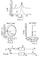
Figure 1 represents a device according to one embodiment of the invention; -
Figure 2 is a simplified view of the device represented onFigure 1 ; -
Figure 3 is a graph illustrating simulated input impedance in a device according to one embodiment of the invention, versus frequency; -
Figure 4 is a graph showing simulated input impedance of a device according to one embodiment of the invention, versus frequency; -
Figure 5 a graph showing simulated attenuation in decibels of input voltage in a device according to one embodiment of the invention, versus frequency; -
Figure 6 is a Nyquist diagram of loop gain expression for a device according to one embodiment of the invention; -
Figure 7 a diagram representing input impedances for different parameters of a device according to one embodiment of the invention, versus frequency; -
Figure 8 is a model representing different noise sources in a device according to one embodiment of the invention. - Referring to
Figure 1 , there is shown therein adevice 1 according to an embodiment of the present invention. Thedevice 1 represented here can be a receiver that comprises, in one embodiment, a direct path block with an input being coupled to an input of thereceiver 1, and an output coupled to an output of thereceiver 1, comprising afirst amplifier 2, amixer 4 and asecond amplifier 6, and a feedback block, with an input and an output, comprising a feedback filter 3, a feedback mixer 5 and a feedback amplifier 7. The output of the direct path block can be coupled to the input of the feedback block and the input of the direct path block can be coupled to the output of the feedback block.Receiver 1 input can be coupled to an antenna 8 adapted to receive and deliver toreceiver 1 radio frequency signals with a given frequency range among a plurality of frequency ranges.Receiver 1 can be adapted to provide an output signal filtered and transposed to a base band frequency range to be further filtered by afilter 9 and transmitted to an analogical-to-digital converter 10 in order to be digitally processed by a system comprising thereceiver 1 for example. - No restriction can be attached to the types of amplifiers, mixers or filters that are comprised in
receiver 1. In one embodiment of the invention,first amplifier 2 is a Low Noise Amplifier adapted to amplify the input signal that is received from the antenna 8. -
Amplifier 2 can be adapted to receive an input signal obtained on the basis of a signal provided by the antenna 8 and a signal provided by the feedback amplifier 7. In the example represented onfigure 2 , both signals can be summed or subtracted to obtain input signal ofamplifier 2.Low Noise Amplifier 2 can also be configured to provide an amplified signal that is transmitted to themixer 4. In one embodiment,first mixer 4 is adapted to receive the amplified signal fromamplifier 2 and a signal with frequency fLO, which is provided by a common oscillator 11. The frequency of the signal delivered by the common oscillator 11 can be configurable and thus adapted to the frequency range of the input signal. For example, a table can associate a frequency fLO to each of the frequency ranges that can be received byreceiver 1 and can be used to adapt frequency fLO to the received signal. In one embodiment, themixer 4 is adapted to generate a mixed signal obtained by translating the amplified signal around frequency fLO, in a base band frequency range (lower frequencies) in order to be further processed. Thus, the receiver is adapted to process signals with a plurality of frequency ranges insofar as the common oscillator 11 can be configurable to transpose the received signal to the base band frequency range. - The mixed signal can then be transmitted to the
second amplifier 6.Second amplifier 6 is configured to output a second amplified signal, where the part of the signal in the base band frequencies is amplified, in order to be transmitted to thefilter 9 and to an input of the feedback filter 3. Feedback filter 3 is adapted to output a filtered signal based on the received amplified signal and to transmit the filtered signal to the feedback mixer 5. Depending on the nature of the feedback, respectively positive or negative, feedback filter 3 can be a low-pass filter or a high-pass filter. Feedback mixer 5 can be configured to receive the filtered signal and also a signal outputted an oscillator. On the example represented here, the common oscillator 11 outputs signals with frequency fLO to be mixed by bothmixer 4 and feedback mixer 5.Feedback mixer 4 is configured to output a second mixed signal based on the filtered signal and the signal with frequency fLO, which enables to transpose the base band signal to the same frequency range as the given frequency range of the input signal outputted by antenna 8 for example. The mixed signal is transmitted to the feedback amplifier 7, which can be for example a trans-conductance amplifier adapted to output a signal which is added or subtracted to the signal provided by antenna 8 and transmitted to thefirst amplifier 2. - The operation of
receiver 1 will be better understood in view ofFigure 2 representing a simplified view of thereceiver 1 according to one embodiment of the invention. -
Receiver 1 is modelled by acircuit 20.Amplifier 2 input impedance is represented in this embodiment by acomponent 24 of impedance ZLNA and coupled to the ground. - Antenna 8 is modelled by a
voltage source 21 with series impedance ZANT being a ratio of a voltage Vant, betweenvoltage source 21 input and the ground, on an intensity iin running through thevoltage source 21. - The direct path block of
receiver 1 can be represented by atransfer filter 22 with a voltage gain G that can be obtained by:
- GLNA is the voltage gain of the
first amplifier 2, - Gmix is the voltage gain of the
mixer 4, and - Gamp is the voltage gain of the
second amplifier 6. - Feedback block is modelled by a
component 23, with trans-conductance being defined by:
where iFB is the current running through thecomponent 23, - VBB is the voltage between the output of the direct path block and the ground,
- Gfil is the voltage gain of the feedback filter 3, which depends on the frequency of the signal received from the
second amplifier 6, - Gmix is the voltage gain of the
feedback mixer 6, which, in this example, equals the voltage gain of themixer 4. - gOTA is the trans-conductance of feedback amplifier 7, which is defined by the ratio of the intensity iFB on the voltage across the feedback amplifier 7.
- Both the path through the direct path block and the path through the feedback block go through a mixer stage (respectively implemented by
mixer 4 and by feedback mixer 5) with identical frequency fLO. In practice, the common mixer stage can be implemented as quadrature direct conversion architecture. - The feedback block represented by
component 23 can add impedance ZFB in parallel to the impedance ZLNA ofcomponent 24, impedance ZFB being given by:
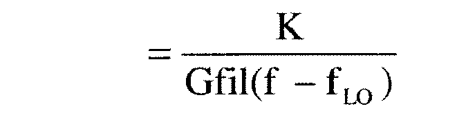

- Then, input impedance, being defined by the ratio of voltage input Vin on the input intensity iin, depending on the frequency, is given by:

-
Amplifier 2 being defined, and thus impedance ZLNA being fixed,receiver 1 can be designed in such a way that input impedance ZIN matches antenna impedance ZANT only in the frequency band of a desired channel, that is, in the frequency range of the input signal received from antenna 8. Signals that are out of the given frequency range or desired range, also called out-of-band signals, are then filtered on the input of theamplifier 2 due to the impedance mismatch. - In a first configuration of the
receiver 1, the amplified signal provided by feedback amplifier 7 is subtracted from the signal provided by antenna 8, to cancel signals that are out of the frequency range of the given signal. Different results can be obtained, depending on the type of feedback filter 3 that is used. - In a first example, feedback filter 3 is a first order low-pass filter implemented for example with a resistor of value R and a capacitor of capacitance C, defined by a function LLp(f), and a function LBP(f) which is the mathematical expression of a first order low-pass filter translated around FLO :


- By replacing this expression in the expression of the feedback impedance Z FB1(f) , the following result is obtained:

- Thus, the input impedance Z IN1(f) can be expressed by:

- Considering now a second example where feedback filter 3 is a first order high pass filter implemented, for example, with a resistor of value R and a capacitor of capacitance C defined by a function HHP(f) and a function HBP(f) which is the mathematical expression of a first order high-pass filter translated around FLO:


- By replacing this expression successively in the expression of the feedback impedance and of the input impedance Z IN2(f), the following result is obtained:

- Referring to
Figure 3 , there is shown a graph illustrating simulated input impedance in thereceiver 1 for a low-pass filter and a high-pass filter according to the examples previously introduced, versus frequency. In this example, parameters of the feedback block are set to achieve a matching between input impedance ZIN and antenna impedance ZANT only in a selective band around frequency fLO, depending on the following data:
- A
first curve 31 represents the result of a simulation for a first order high-pass filter, with K=150Ω. Asecond curve 32 represents the result of a simulation for a first order low-pass filter with K=855Ω. A matching between input impedances ZIN2 and ZIN1 and antenna impedance ZANT is made in both cases in a band around frequency fLO. Onsecond curve 32, input impedance ZIN1 increases when frequency moves away from fLO, thus enabling to reduce the gain for out-of-band signals. Onfirst curve 31, input impedance ZIN2 decreases when frequency moves away from fLO. - In a second configuration of the
receiver 1, the amplified signal provided by feedback amplifier 7 is added to the signal provided by antenna 8. - In this embodiment, feedback filter 3 is a first order low-pass filter implemented for example with a resistor of value R and a capacitor of capacitance C, defined by a function LLP(f), and a function LBP(f) which is the mathematical expression of a first order low-pass filter translated around FLO :


- By replacing this expression in the expression of the feedback impedance zFB3 (f) for a positive feedback changing the sign of current iFB, the following result is obtained:

- Thus, the input impedance Z IN3(f) can be expressed by:

- Impedance ZLNA can be chosen smaller than ZANT to reject ou-of-band signals. By increasing the difference between these impedances, the attenuation of the ou-of-band signals is improved.
- Referring now to
Figure 4 andFigure 5 , the simulated results for a first order low-pass filter in the case of a positive feedback are considered. The following parameters are considered in this example:
-
Figure 4 is a graph showing simulated input impedance versus frequency for a first order low-pass filter inreceiver 1 for positive feedback represented by a third curve 41 with K=12,4 Ω and ZLNA=10 Ω and for a first order low-pass filter represented byfourth curve 42 with K=3,2 Ω and ZLNA=3 Ω.Figure 5 is a graph showing simulated attenuation in decibels (dB) of input voltage for a first order low-pass filter inreceiver 1 with positive feedback represented by afifth curve 51 with K=12,4 Ω and ZLNA=10 Ω and for a first order low-pass filter represented bysixth curve 52 with K=3,2 Ω and ZLNA=3 Ω, versus frequency. - A matching between input impedance ZIN3 and antenna impedance ZANT is obtained for a feedback low-pass filter in a narrow band around fLO:

- Consequently,
receiver 1 attenuates the signals that are out of the given frequency range of the input signal (also called out-of-band signals). The attenuation can depend on the initial value of impedance ZLNA and can be given by:
- Referring to
figure 5 , in the case of a low-pass filter illustrated onsixth curve 52, the attenuation obtained is around 19dB. - The advantage of the positive feedback is the attenuation of every signals by default if impedance ZLNA is smaller than impedance ZANT. The positive feedback allows matching the device with the antenna impedance ZANT only in the band defined by the low-pass filter of the feedback block. Then, bandwidth loop does not limit the performance of the system because the impedance is only modified for frequency around the signal and the out-of-band signals are filtered as the loop does not work for higher frequency. In the case of negative feedback (HP Filter), feedback block must work at higher frequency than all out-of-band interferers.
- The stability of the
receiver 1 can be studied by analyzing loop gain expression S(f) in open-loop given by:
- A stability condition can be given by:

- The stability of such architecture of
receiver 1 depends on the value of K. - Referring now to
Figure 6 , a Nyquist diagram of loop gain expression S(f) forreceiver 1 with positive feedback is represented with afirst circle 61, asecond circle 62 and athird circle 63, respectively for three different values of K, namely K1=3,2 Ω, K2=3,09 Ω and K3=Ω, and with ZLNA=3 Ω and ZANT=50 Ω. - If a circle encloses the point defined by coordinates (-1,0), the architecture is unstable. Thus, for the value K3 corresponding to
third circle 63, the system is unstable. For the two other values of K1 and K2, corresponding to the first and thesecond circles receiver 1, and in particular of feedback block, as trans-conductance value gr for example, can be determined so that architecture ofreceiver 1 is unconditionally stable. - Referring now to
Figure 7 , a diagram representing input impedance versus frequency for the different values K1, K2 and K3, respectively represented by seventh curve 71,eighth curve 72 andninth curve 73, forreceiver 1 with positive feedback, can be considered. In the case of K2, for which the architecture ofreceiver 1 is stable, a strong output signal is fed to the input ofreceiver 1. Impedance ZIN becomes larger than ZANT and the impedance matching of the device is not achieved. Parameters ofreceiver 1 and in particular of feedback block, can be determined so that input impedance ZIN is set to impedance value ZANT. Thus, positive feedback in a receiver according to the invention enables to improve radio frequency filtering attenuation and selectivity for out-of-band signals, when parameters of the feedback block are adjusted depending on the initial value of impedance ZLNA, which is constrained byLow Noise Amplifier 2 design trade off, and on stability considerations. The attenuation depends on the value between impedance ZANT and ZLNA. To improve the attenuation of the out-of-band signals the ZLNA should be lower as possible. Selectivity can depend on the cut-off frequency fC, which can be, joined with frequency fLO, configurable for multi-standard and multi-band applications. With realistic values for the various parameters, an attenuation of out-of-band signals of up to -19dB can be obtained. - Referring to
figure 8 ,receiver 1 with positive feedback is modelled to illustrate the different sources of noise, respectively input noise Xs, direct path noise X1 at the input of direct path block 81, feedback noise X2 at the input offeedback block 81, and output noise Xo at the output ofreceiver 1. - Considering voltage noise sources in a band of 1 Hz, the output noise is given by:

feedback block 82. - Then, noise figure FFB in
feedback block 82 can be defined according to North definition by:
- Such analysis shows the variation of noise figure in
receiver 1 with positive feedback.Feedback block 82 increases the noise in the given frequency range of the received signal (in-band) due to noisy output signal brought to the input ofreceiver 1. In a real application, gain A can be large. Then, gain B will be chosen small, preferably smaller than 1, to decrease the noise and ensure stability. Thus, the dominant noise contributor will be the direct path block 81, and in particularLow Noise Amplifier 2 and noise impact of the invention can be made small. Thus, the global noise of the system can be assimilated to the direct path noise X1. - The present invention can also be embedded in a computer program product, which comprises all the features enabling the implementation of the methods described herein, and which, when loaded in an information processing system, causes the information processing system. Computer program means or computer program in the present context mean any expression, in any language, code or notation, of a set of instructions intended to cause a system having an information processing capability to perform a particular function either directly or after either or both of the following a) conversion to another language. Such a computer program can be stored on a computer or machine readable medium allowing data, instructions, messages or message packets, and other machine readable information to be read from the medium. The computer or machine readable medium may include non-volatile memory, such as ROM, Flash memory, Disk drive memory, CD-ROM, and other permanent storage. Additionally, a computer or machine readable medium may include, for example, volatile storage such as RAM, buffers, cache memory, and network circuits. Furthermore, the computer or machine readable medium may comprise computer or machine readable information in a transitory state medium such as a network link and/or a network interface, including a wired network or a wireless network, that allow a device to read such computer or machine readable information.
- Expressions such as "comprise", "include", "incorporate", "contain", "is" and "have" are to be construed in a non-exclusive manner when interpreting the description and its associated claims, namely construed to allow for other items or components which are not explicitly defined also to be present. Reference to the singular is also to be construed in be a reference to the plural and vice versa.
- While there has been illustrated and described what are presently considered to be the preferred embodiments of the present invention, it will be understood by those skilled in the art that various other modifications may be made, and equivalents may be substituted, without departing from the true scope of the present invention. Additionally, many modifications may be made to adapt a particular situation to the teachings of the present invention without departing from the central inventive concept described herein. Furthermore, an embodiment of the present invention may not include all of the features described above. Therefore, it is intended that the present invention not be limited to the particular embodiments disclosed, but that the invention include all embodiments falling within the scope of the invention as broadly defined above.
- A person skilled in the art will readily appreciate that various parameters disclosed in the description may be modified and that various embodiments disclosed and/or claimed may be combined without departing from the scope of the invention.
Claims (12)
- A device comprising a direct path block (81) with an input and an output, and a feedback block (82) with an input and an output, the input of the direct path block being adapted to receive a multi-channel input signal with a given frequency range and the output of the direct path block being adapted to output an output signal with a base band frequency range, the output of the direct path block being coupled to the input of the feedback block and the input of the direct path block being coupled to the output of the feedback block, wherein:- the direct path block comprises a first transposing unit (4) adapted to transpose the input signal to the base band frequency range,- the feedback block comprises a filtering unit (3) adapted to filter the transposed signal at the output of the direct path block, a second transposing unit (5) adapted to transpose the filtered signal to the given frequency range and to feed back the transposed signal at the input of the direct path block, and- the first transposing unit and the second transposing unit are reconfigurable in function of the given frequency range of the input signal.
- The device of claim 1, wherein the first transposing unit (4) and the second transposing unit (5) comprise a first mixer and a second mixer, respectively, and a common oscillator (11) coupled to the first mixer and to the second mixer.
- The device of claim 2, wherein the oscillator (11) delivers a signal at a frequency, which depends dynamically on the given frequency range of the input signal.
- The device according to one of claims 1 to 3, wherein the direct path block (81) further comprises an amplifying unit (2) adapted to amplify the input signal at the input of the direct path block.
- The device according to one of claims 1 to 4, wherein the filtering unit (3) is a low-pass filter and the transposed signal is positively fed back at the input of the direct path block.
- The device according to one of claims 1 to 5, wherein the feedback block (82) further comprises a feedback amplifier (7) adapted to amplify the transposed signal and to feed back the amplified signal at the input of the direct path block.
- The device according to one of claims 1 to 6, wherein parameters of the feedback block (82) are determined so that an input impedance defined by the ratio of a voltage at the input of the device on an input current at the input of the device, is set to a given value.
- The device according to one of claims 1 to 7, wherein the device is a wide band receiver.
- A method being implemented by a device comprising a direct path block (81) with an input and an output, and a feedback block (82) with an input and an output, being adapted to receive a multi-channel input signal with a given frequency range and being adapted to output an output signal with a base band frequency range, the output of the direct path block being coupled to the input of the feedback block and the input of the direct path block being coupled to the output of the feedback block, wherein the method comprises :- receiving an input signal with a given frequency range at the input of the direct path block ;- transposing the input signal to the base band frequency range at the input of the feedback block;- filtering the transposed signal;- transposing the filtered signal to the given radio frequency range; and- feeding back the transposed signal at the input of the direct path block;the transposing of the input signal to the base band frequency and the transposing of the filtered signal to the radio frequency range being function of the frequency range of the input signal.
- The method of claim 9, wherein the filtering of the transposed signal is a low-pass filtering and the feeding back is positive.
- The method according to one of claims 9 and 10, wherein parameters of the feedback block (82) are configured so that an input impedance defined by the ratio of a voltage at the input of the device on an input current at the input of the device, is set to a given value.
- A system comprising a device according to anyone of claims 1 to 8, a receiving unit (8) adapted to receive an input signal with a given frequency range and adapted to provide the device with the input signal, and an output filtering unit (9) adapted to filter the output signal at the output of the device.
Priority Applications (3)
| Application Number | Priority Date | Filing Date | Title |
|---|---|---|---|
| EP10194629.1A EP2445113B1 (en) | 2010-10-22 | 2010-12-10 | Reconfigurable wide-band radio receiver with positive feed-back translational loop |
| US13/879,720 US8787852B2 (en) | 2010-10-22 | 2011-10-20 | Reconfigurable wide-band receiver with positive feed-back translational loop |
| PCT/EP2011/068361 WO2012052520A1 (en) | 2010-10-22 | 2011-10-20 | Reconfigurable wide-band receiver with positive feed-back translational loop |
Applications Claiming Priority (2)
| Application Number | Priority Date | Filing Date | Title |
|---|---|---|---|
| EP10306158 | 2010-10-22 | ||
| EP10194629.1A EP2445113B1 (en) | 2010-10-22 | 2010-12-10 | Reconfigurable wide-band radio receiver with positive feed-back translational loop |
Publications (2)
| Publication Number | Publication Date |
|---|---|
| EP2445113A1 true EP2445113A1 (en) | 2012-04-25 |
| EP2445113B1 EP2445113B1 (en) | 2016-08-31 |
Family
ID=45444798
Family Applications (1)
| Application Number | Title | Priority Date | Filing Date |
|---|---|---|---|
| EP10194629.1A Not-in-force EP2445113B1 (en) | 2010-10-22 | 2010-12-10 | Reconfigurable wide-band radio receiver with positive feed-back translational loop |
Country Status (3)
| Country | Link |
|---|---|
| US (1) | US8787852B2 (en) |
| EP (1) | EP2445113B1 (en) |
| WO (1) | WO2012052520A1 (en) |
Cited By (2)
| Publication number | Priority date | Publication date | Assignee | Title |
|---|---|---|---|---|
| CN105577258A (en) * | 2014-10-31 | 2016-05-11 | 天工方案公司 | Diversity Receiver Front End System With Switching Network |
| CN115085750A (en) * | 2022-06-09 | 2022-09-20 | 广东圣大电子有限公司 | Anti-blocking radio receiver |
Families Citing this family (7)
| Publication number | Priority date | Publication date | Assignee | Title |
|---|---|---|---|---|
| US9479132B2 (en) * | 2014-04-15 | 2016-10-25 | Broadcom Corporation | Signal conversion with gain in the forward path |
| JP6029728B2 (en) * | 2014-10-31 | 2016-11-24 | スカイワークス ソリューションズ,インコーポレイテッドSkyworks Solutions,Inc. | Diversity receiver front-end system with phase shift components |
| US9385765B2 (en) | 2014-10-31 | 2016-07-05 | Skyworks Solutions, Inc. | Diversity receiver front end system with phase-shifting components |
| US10050694B2 (en) | 2014-10-31 | 2018-08-14 | Skyworks Solution, Inc. | Diversity receiver front end system with post-amplifier filters |
| US9893752B2 (en) | 2014-10-31 | 2018-02-13 | Skyworks Solutions, Inc. | Diversity receiver front end system with variable-gain amplifiers |
| US9838056B2 (en) | 2015-05-28 | 2017-12-05 | Skyworks Solutions, Inc. | Integrous signal combiner |
| JP6720527B2 (en) * | 2015-12-25 | 2020-07-08 | 富士通株式会社 | Amplifying circuit, optical module and amplifying method |
Citations (2)
| Publication number | Priority date | Publication date | Assignee | Title |
|---|---|---|---|---|
| US4718113A (en) * | 1985-05-08 | 1988-01-05 | Alcatel Nv | Zero-IF receiver wih feedback loop for suppressing interfering signals |
| US20090156152A1 (en) * | 2007-12-12 | 2009-06-18 | Qualcomm Incorporated | Tracking filter for a receiver |
Family Cites Families (6)
| Publication number | Priority date | Publication date | Assignee | Title |
|---|---|---|---|---|
| GB2296613A (en) * | 1994-12-21 | 1996-07-03 | Univ Bristol | Image-reject mixers |
| US5822704A (en) * | 1996-01-05 | 1998-10-13 | Nec Corporation | Mobile radio unit for use in dual-mode cellular communications system |
| US5982807A (en) * | 1997-03-17 | 1999-11-09 | Harris Corporation | High data rate spread spectrum transceiver and associated methods |
| US6778594B1 (en) * | 2000-06-12 | 2004-08-17 | Broadcom Corporation | Receiver architecture employing low intermediate frequency and complex filtering |
| US7187230B2 (en) | 2005-03-18 | 2007-03-06 | Nokia Corporation | Transferred-impedance filtering in RF receivers |
| EP2204907A1 (en) | 2008-12-30 | 2010-07-07 | ST Wireless SA | Amplifier with on-chip filter |
-
2010
- 2010-12-10 EP EP10194629.1A patent/EP2445113B1/en not_active Not-in-force
-
2011
- 2011-10-20 US US13/879,720 patent/US8787852B2/en not_active Expired - Fee Related
- 2011-10-20 WO PCT/EP2011/068361 patent/WO2012052520A1/en not_active Ceased
Patent Citations (2)
| Publication number | Priority date | Publication date | Assignee | Title |
|---|---|---|---|---|
| US4718113A (en) * | 1985-05-08 | 1988-01-05 | Alcatel Nv | Zero-IF receiver wih feedback loop for suppressing interfering signals |
| US20090156152A1 (en) * | 2007-12-12 | 2009-06-18 | Qualcomm Incorporated | Tracking filter for a receiver |
Cited By (4)
| Publication number | Priority date | Publication date | Assignee | Title |
|---|---|---|---|---|
| CN105577258A (en) * | 2014-10-31 | 2016-05-11 | 天工方案公司 | Diversity Receiver Front End System With Switching Network |
| CN105577258B (en) * | 2014-10-31 | 2019-03-22 | 天工方案公司 | Diversity receiver front end system with switching network |
| CN115085750A (en) * | 2022-06-09 | 2022-09-20 | 广东圣大电子有限公司 | Anti-blocking radio receiver |
| CN115085750B (en) * | 2022-06-09 | 2023-08-15 | 广东圣大电子有限公司 | Anti-blocking radio receiver |
Also Published As
| Publication number | Publication date |
|---|---|
| WO2012052520A1 (en) | 2012-04-26 |
| EP2445113B1 (en) | 2016-08-31 |
| US20130281039A1 (en) | 2013-10-24 |
| US8787852B2 (en) | 2014-07-22 |
Similar Documents
| Publication | Publication Date | Title |
|---|---|---|
| US8787852B2 (en) | Reconfigurable wide-band receiver with positive feed-back translational loop | |
| CN108233952B (en) | Communication module | |
| US8644785B2 (en) | Filtering using impedance translator | |
| US5678213A (en) | Radio receiver for processing a multi-carrier signal with a large dynamic range | |
| CN101895329A (en) | Duplexer and switch strengthen | |
| US20190158042A1 (en) | Gain-Dependent Impedance Matching and Linearity | |
| US11128333B2 (en) | Signal receiving circuit, signal processing chip, communications device, and signal receiving method | |
| US10505702B2 (en) | Transmission/reception module | |
| US9979420B1 (en) | Receiver with multi-spectrum parallel amplification | |
| EP1724936A2 (en) | Matching circuit | |
| JP4447321B2 (en) | Impedance matching circuit for multiband radio frequency equipment | |
| US9300265B2 (en) | Wireless communication device, method and power amplifier of the same | |
| KR20180125842A (en) | Multi-band radio-frequency transmitter with receiving band variable filtering function | |
| KR101536689B1 (en) | Interference signal removing apparatus and RF receiver using thereof | |
| WO2018031198A1 (en) | Multi-stage bandpass low-noise amplifier | |
| US20160269052A1 (en) | Supporting multiple frequency bands | |
| US9787334B2 (en) | High frequency power amplifier, high frequency front-end circuit, and radio communication device | |
| WO2019235181A1 (en) | Radio frequency front-end module and communication device | |
| US7127226B2 (en) | Twin-T dual notch filter | |
| CN101213760B (en) | Apparatus and method for input third-order intercept point control of a wireless transceiver | |
| US11804863B2 (en) | Radio-frequency signal transmission/reception circuit and radio-frequency signal transmission/reception device | |
| CN216672973U (en) | High-frequency module and communication device | |
| KR20080030658A (en) | Compact mixer output stage for high dynamic range wireless receivers | |
| KR20150042512A (en) | Method and apparatud for controlling operation mode of receiver in an electronic device | |
| EP4333295B1 (en) | Tunable bandpass low noise amplifier |
Legal Events
| Date | Code | Title | Description |
|---|---|---|---|
| AK | Designated contracting states |
Kind code of ref document: A1 Designated state(s): AL AT BE BG CH CY CZ DE DK EE ES FI FR GB GR HR HU IE IS IT LI LT LU LV MC MK MT NL NO PL PT RO RS SE SI SK SM TR |
|
| AX | Request for extension of the european patent |
Extension state: BA ME |
|
| PUAI | Public reference made under article 153(3) epc to a published international application that has entered the european phase |
Free format text: ORIGINAL CODE: 0009012 |
|
| 17P | Request for examination filed |
Effective date: 20120924 |
|
| GRAP | Despatch of communication of intention to grant a patent |
Free format text: ORIGINAL CODE: EPIDOSNIGR1 |
|
| INTG | Intention to grant announced |
Effective date: 20160418 |
|
| GRAS | Grant fee paid |
Free format text: ORIGINAL CODE: EPIDOSNIGR3 |
|
| GRAA | (expected) grant |
Free format text: ORIGINAL CODE: 0009210 |
|
| AK | Designated contracting states |
Kind code of ref document: B1 Designated state(s): AL AT BE BG CH CY CZ DE DK EE ES FI FR GB GR HR HU IE IS IT LI LT LU LV MC MK MT NL NO PL PT RO RS SE SI SK SM TR |
|
| REG | Reference to a national code |
Ref country code: CH Ref legal event code: EP Ref country code: GB Ref legal event code: FG4D |
|
| REG | Reference to a national code |
Ref country code: IE Ref legal event code: FG4D |
|
| REG | Reference to a national code |
Ref country code: DE Ref legal event code: R096 Ref document number: 602010035951 Country of ref document: DE |
|
| REG | Reference to a national code |
Ref country code: AT Ref legal event code: REF Ref document number: 825757 Country of ref document: AT Kind code of ref document: T Effective date: 20161015 |
|
| REG | Reference to a national code |
Ref country code: FR Ref legal event code: PLFP Year of fee payment: 7 |
|
| REG | Reference to a national code |
Ref country code: LT Ref legal event code: MG4D |
|
| REG | Reference to a national code |
Ref country code: NL Ref legal event code: MP Effective date: 20160831 |
|
| REG | Reference to a national code |
Ref country code: DE Ref legal event code: R082 Ref document number: 602010035951 Country of ref document: DE Representative=s name: GRUENECKER PATENT- UND RECHTSANWAELTE PARTG MB, DE Ref country code: DE Ref legal event code: R081 Ref document number: 602010035951 Country of ref document: DE Owner name: OCT CIRCUIT TECHNOLOGIES INTERNATIONAL LTD., IE Free format text: FORMER OWNER: ST-ERICSSON SA, PLAN-LES-OUATES, CH |
|
| REG | Reference to a national code |
Ref country code: AT Ref legal event code: MK05 Ref document number: 825757 Country of ref document: AT Kind code of ref document: T Effective date: 20160831 |
|
| RAP2 | Party data changed (patent owner data changed or rights of a patent transferred) |
Owner name: OCT CIRCUIT TECHNOLOGIES INTERNATIONAL LIMITED |
|
| PG25 | Lapsed in a contracting state [announced via postgrant information from national office to epo] |
Ref country code: RS Free format text: LAPSE BECAUSE OF FAILURE TO SUBMIT A TRANSLATION OF THE DESCRIPTION OR TO PAY THE FEE WITHIN THE PRESCRIBED TIME-LIMIT Effective date: 20160831 Ref country code: NO Free format text: LAPSE BECAUSE OF FAILURE TO SUBMIT A TRANSLATION OF THE DESCRIPTION OR TO PAY THE FEE WITHIN THE PRESCRIBED TIME-LIMIT Effective date: 20161130 Ref country code: LT Free format text: LAPSE BECAUSE OF FAILURE TO SUBMIT A TRANSLATION OF THE DESCRIPTION OR TO PAY THE FEE WITHIN THE PRESCRIBED TIME-LIMIT Effective date: 20160831 Ref country code: FI Free format text: LAPSE BECAUSE OF FAILURE TO SUBMIT A TRANSLATION OF THE DESCRIPTION OR TO PAY THE FEE WITHIN THE PRESCRIBED TIME-LIMIT Effective date: 20160831 Ref country code: HR Free format text: LAPSE BECAUSE OF FAILURE TO SUBMIT A TRANSLATION OF THE DESCRIPTION OR TO PAY THE FEE WITHIN THE PRESCRIBED TIME-LIMIT Effective date: 20160831 |
|
| PG25 | Lapsed in a contracting state [announced via postgrant information from national office to epo] |
Ref country code: LV Free format text: LAPSE BECAUSE OF FAILURE TO SUBMIT A TRANSLATION OF THE DESCRIPTION OR TO PAY THE FEE WITHIN THE PRESCRIBED TIME-LIMIT Effective date: 20160831 Ref country code: NL Free format text: LAPSE BECAUSE OF FAILURE TO SUBMIT A TRANSLATION OF THE DESCRIPTION OR TO PAY THE FEE WITHIN THE PRESCRIBED TIME-LIMIT Effective date: 20160831 Ref country code: ES Free format text: LAPSE BECAUSE OF FAILURE TO SUBMIT A TRANSLATION OF THE DESCRIPTION OR TO PAY THE FEE WITHIN THE PRESCRIBED TIME-LIMIT Effective date: 20160831 Ref country code: AT Free format text: LAPSE BECAUSE OF FAILURE TO SUBMIT A TRANSLATION OF THE DESCRIPTION OR TO PAY THE FEE WITHIN THE PRESCRIBED TIME-LIMIT Effective date: 20160831 Ref country code: GR Free format text: LAPSE BECAUSE OF FAILURE TO SUBMIT A TRANSLATION OF THE DESCRIPTION OR TO PAY THE FEE WITHIN THE PRESCRIBED TIME-LIMIT Effective date: 20161201 Ref country code: SE Free format text: LAPSE BECAUSE OF FAILURE TO SUBMIT A TRANSLATION OF THE DESCRIPTION OR TO PAY THE FEE WITHIN THE PRESCRIBED TIME-LIMIT Effective date: 20160831 |
|
| PG25 | Lapsed in a contracting state [announced via postgrant information from national office to epo] |
Ref country code: EE Free format text: LAPSE BECAUSE OF FAILURE TO SUBMIT A TRANSLATION OF THE DESCRIPTION OR TO PAY THE FEE WITHIN THE PRESCRIBED TIME-LIMIT Effective date: 20160831 Ref country code: RO Free format text: LAPSE BECAUSE OF FAILURE TO SUBMIT A TRANSLATION OF THE DESCRIPTION OR TO PAY THE FEE WITHIN THE PRESCRIBED TIME-LIMIT Effective date: 20160831 |
|
| PG25 | Lapsed in a contracting state [announced via postgrant information from national office to epo] |
Ref country code: BG Free format text: LAPSE BECAUSE OF FAILURE TO SUBMIT A TRANSLATION OF THE DESCRIPTION OR TO PAY THE FEE WITHIN THE PRESCRIBED TIME-LIMIT Effective date: 20161130 Ref country code: BE Free format text: LAPSE BECAUSE OF FAILURE TO SUBMIT A TRANSLATION OF THE DESCRIPTION OR TO PAY THE FEE WITHIN THE PRESCRIBED TIME-LIMIT Effective date: 20160831 Ref country code: PT Free format text: LAPSE BECAUSE OF FAILURE TO SUBMIT A TRANSLATION OF THE DESCRIPTION OR TO PAY THE FEE WITHIN THE PRESCRIBED TIME-LIMIT Effective date: 20170102 Ref country code: CZ Free format text: LAPSE BECAUSE OF FAILURE TO SUBMIT A TRANSLATION OF THE DESCRIPTION OR TO PAY THE FEE WITHIN THE PRESCRIBED TIME-LIMIT Effective date: 20160831 Ref country code: DK Free format text: LAPSE BECAUSE OF FAILURE TO SUBMIT A TRANSLATION OF THE DESCRIPTION OR TO PAY THE FEE WITHIN THE PRESCRIBED TIME-LIMIT Effective date: 20160831 Ref country code: SM Free format text: LAPSE BECAUSE OF FAILURE TO SUBMIT A TRANSLATION OF THE DESCRIPTION OR TO PAY THE FEE WITHIN THE PRESCRIBED TIME-LIMIT Effective date: 20160831 Ref country code: SK Free format text: LAPSE BECAUSE OF FAILURE TO SUBMIT A TRANSLATION OF THE DESCRIPTION OR TO PAY THE FEE WITHIN THE PRESCRIBED TIME-LIMIT Effective date: 20160831 Ref country code: PL Free format text: LAPSE BECAUSE OF FAILURE TO SUBMIT A TRANSLATION OF THE DESCRIPTION OR TO PAY THE FEE WITHIN THE PRESCRIBED TIME-LIMIT Effective date: 20160831 |
|
| REG | Reference to a national code |
Ref country code: DE Ref legal event code: R097 Ref document number: 602010035951 Country of ref document: DE |
|
| PG25 | Lapsed in a contracting state [announced via postgrant information from national office to epo] |
Ref country code: IT Free format text: LAPSE BECAUSE OF FAILURE TO SUBMIT A TRANSLATION OF THE DESCRIPTION OR TO PAY THE FEE WITHIN THE PRESCRIBED TIME-LIMIT Effective date: 20160831 |
|
| PLBE | No opposition filed within time limit |
Free format text: ORIGINAL CODE: 0009261 |
|
| STAA | Information on the status of an ep patent application or granted ep patent |
Free format text: STATUS: NO OPPOSITION FILED WITHIN TIME LIMIT |
|
| REG | Reference to a national code |
Ref country code: CH Ref legal event code: PL |
|
| 26N | No opposition filed |
Effective date: 20170601 |
|
| PG25 | Lapsed in a contracting state [announced via postgrant information from national office to epo] |
Ref country code: SI Free format text: LAPSE BECAUSE OF FAILURE TO SUBMIT A TRANSLATION OF THE DESCRIPTION OR TO PAY THE FEE WITHIN THE PRESCRIBED TIME-LIMIT Effective date: 20160831 |
|
| PG25 | Lapsed in a contracting state [announced via postgrant information from national office to epo] |
Ref country code: MC Free format text: LAPSE BECAUSE OF FAILURE TO SUBMIT A TRANSLATION OF THE DESCRIPTION OR TO PAY THE FEE WITHIN THE PRESCRIBED TIME-LIMIT Effective date: 20160831 |
|
| REG | Reference to a national code |
Ref country code: IE Ref legal event code: MM4A |
|
| PG25 | Lapsed in a contracting state [announced via postgrant information from national office to epo] |
Ref country code: CH Free format text: LAPSE BECAUSE OF NON-PAYMENT OF DUE FEES Effective date: 20161231 Ref country code: LU Free format text: LAPSE BECAUSE OF NON-PAYMENT OF DUE FEES Effective date: 20161210 Ref country code: LI Free format text: LAPSE BECAUSE OF NON-PAYMENT OF DUE FEES Effective date: 20161231 |
|
| REG | Reference to a national code |
Ref country code: FR Ref legal event code: PLFP Year of fee payment: 8 |
|
| PG25 | Lapsed in a contracting state [announced via postgrant information from national office to epo] |
Ref country code: IE Free format text: LAPSE BECAUSE OF NON-PAYMENT OF DUE FEES Effective date: 20161210 |
|
| PGFP | Annual fee paid to national office [announced via postgrant information from national office to epo] |
Ref country code: FR Payment date: 20171121 Year of fee payment: 8 Ref country code: DE Payment date: 20171120 Year of fee payment: 8 |
|
| PGFP | Annual fee paid to national office [announced via postgrant information from national office to epo] |
Ref country code: GB Payment date: 20171121 Year of fee payment: 8 |
|
| PG25 | Lapsed in a contracting state [announced via postgrant information from national office to epo] |
Ref country code: CY Free format text: LAPSE BECAUSE OF FAILURE TO SUBMIT A TRANSLATION OF THE DESCRIPTION OR TO PAY THE FEE WITHIN THE PRESCRIBED TIME-LIMIT Effective date: 20160831 Ref country code: HU Free format text: LAPSE BECAUSE OF FAILURE TO SUBMIT A TRANSLATION OF THE DESCRIPTION OR TO PAY THE FEE WITHIN THE PRESCRIBED TIME-LIMIT; INVALID AB INITIO Effective date: 20101210 |
|
| PG25 | Lapsed in a contracting state [announced via postgrant information from national office to epo] |
Ref country code: TR Free format text: LAPSE BECAUSE OF FAILURE TO SUBMIT A TRANSLATION OF THE DESCRIPTION OR TO PAY THE FEE WITHIN THE PRESCRIBED TIME-LIMIT Effective date: 20160831 Ref country code: MK Free format text: LAPSE BECAUSE OF FAILURE TO SUBMIT A TRANSLATION OF THE DESCRIPTION OR TO PAY THE FEE WITHIN THE PRESCRIBED TIME-LIMIT Effective date: 20160831 Ref country code: IS Free format text: LAPSE BECAUSE OF FAILURE TO SUBMIT A TRANSLATION OF THE DESCRIPTION OR TO PAY THE FEE WITHIN THE PRESCRIBED TIME-LIMIT Effective date: 20160831 |
|
| PG25 | Lapsed in a contracting state [announced via postgrant information from national office to epo] |
Ref country code: MT Free format text: LAPSE BECAUSE OF NON-PAYMENT OF DUE FEES Effective date: 20161210 |
|
| PG25 | Lapsed in a contracting state [announced via postgrant information from national office to epo] |
Ref country code: AL Free format text: LAPSE BECAUSE OF FAILURE TO SUBMIT A TRANSLATION OF THE DESCRIPTION OR TO PAY THE FEE WITHIN THE PRESCRIBED TIME-LIMIT Effective date: 20160831 |
|
| REG | Reference to a national code |
Ref country code: DE Ref legal event code: R119 Ref document number: 602010035951 Country of ref document: DE |
|
| GBPC | Gb: european patent ceased through non-payment of renewal fee |
Effective date: 20181210 |
|
| PG25 | Lapsed in a contracting state [announced via postgrant information from national office to epo] |
Ref country code: FR Free format text: LAPSE BECAUSE OF NON-PAYMENT OF DUE FEES Effective date: 20181231 Ref country code: DE Free format text: LAPSE BECAUSE OF NON-PAYMENT OF DUE FEES Effective date: 20190702 |
|
| PG25 | Lapsed in a contracting state [announced via postgrant information from national office to epo] |
Ref country code: GB Free format text: LAPSE BECAUSE OF NON-PAYMENT OF DUE FEES Effective date: 20181210 |