EP2442445A1 - MEMS oscillator - Google Patents
MEMS oscillator Download PDFInfo
- Publication number
- EP2442445A1 EP2442445A1 EP10187296A EP10187296A EP2442445A1 EP 2442445 A1 EP2442445 A1 EP 2442445A1 EP 10187296 A EP10187296 A EP 10187296A EP 10187296 A EP10187296 A EP 10187296A EP 2442445 A1 EP2442445 A1 EP 2442445A1
- Authority
- EP
- European Patent Office
- Prior art keywords
- resonator
- resonator body
- bias
- output
- current
- Prior art date
- Legal status (The legal status is an assumption and is not a legal conclusion. Google has not performed a legal analysis and makes no representation as to the accuracy of the status listed.)
- Granted
Links
- 238000000034 method Methods 0.000 claims description 13
- 230000008901 benefit Effects 0.000 abstract description 5
- 230000035945 sensitivity Effects 0.000 abstract description 3
- 239000000758 substrate Substances 0.000 description 11
- 238000005530 etching Methods 0.000 description 9
- 238000013461 design Methods 0.000 description 8
- XUIMIQQOPSSXEZ-UHFFFAOYSA-N Silicon Chemical compound [Si] XUIMIQQOPSSXEZ-UHFFFAOYSA-N 0.000 description 5
- 238000005259 measurement Methods 0.000 description 5
- 230000010355 oscillation Effects 0.000 description 5
- 229910052710 silicon Inorganic materials 0.000 description 5
- 239000010703 silicon Substances 0.000 description 5
- 238000004519 manufacturing process Methods 0.000 description 4
- 238000005459 micromachining Methods 0.000 description 4
- 239000010453 quartz Substances 0.000 description 4
- VYPSYNLAJGMNEJ-UHFFFAOYSA-N silicon dioxide Inorganic materials O=[Si]=O VYPSYNLAJGMNEJ-UHFFFAOYSA-N 0.000 description 4
- 230000003321 amplification Effects 0.000 description 3
- 239000013078 crystal Substances 0.000 description 3
- 230000007423 decrease Effects 0.000 description 3
- 238000003199 nucleic acid amplification method Methods 0.000 description 3
- 230000000295 complement effect Effects 0.000 description 2
- 230000001419 dependent effect Effects 0.000 description 2
- 238000001459 lithography Methods 0.000 description 2
- JBRZTFJDHDCESZ-UHFFFAOYSA-N AsGa Chemical compound [As]#[Ga] JBRZTFJDHDCESZ-UHFFFAOYSA-N 0.000 description 1
- 229910001218 Gallium arsenide Inorganic materials 0.000 description 1
- 230000003044 adaptive effect Effects 0.000 description 1
- 230000003466 anti-cipated effect Effects 0.000 description 1
- 238000013459 approach Methods 0.000 description 1
- 239000003989 dielectric material Substances 0.000 description 1
- 230000005489 elastic deformation Effects 0.000 description 1
- 239000011521 glass Substances 0.000 description 1
- 238000010348 incorporation Methods 0.000 description 1
- 230000010354 integration Effects 0.000 description 1
- 229910052751 metal Inorganic materials 0.000 description 1
- 239000007769 metal material Substances 0.000 description 1
- 238000012536 packaging technology Methods 0.000 description 1
- 230000010287 polarization Effects 0.000 description 1
- 239000004065 semiconductor Substances 0.000 description 1
- 230000006641 stabilisation Effects 0.000 description 1
- 239000010409 thin film Substances 0.000 description 1
- 238000000427 thin-film deposition Methods 0.000 description 1
Images



Classifications
-
- H—ELECTRICITY
- H03—ELECTRONIC CIRCUITRY
- H03H—IMPEDANCE NETWORKS, e.g. RESONANT CIRCUITS; RESONATORS
- H03H9/00—Networks comprising electromechanical or electro-acoustic elements; Electromechanical resonators
- H03H9/02—Details
- H03H9/02244—Details of microelectro-mechanical resonators
- H03H9/02259—Driving or detection means
-
- H—ELECTRICITY
- H03—ELECTRONIC CIRCUITRY
- H03B—GENERATION OF OSCILLATIONS, DIRECTLY OR BY FREQUENCY-CHANGING, BY CIRCUITS EMPLOYING ACTIVE ELEMENTS WHICH OPERATE IN A NON-SWITCHING MANNER; GENERATION OF NOISE BY SUCH CIRCUITS
- H03B5/00—Generation of oscillations using amplifier with regenerative feedback from output to input
- H03B5/30—Generation of oscillations using amplifier with regenerative feedback from output to input with frequency-determining element being electromechanical resonator
Definitions
- This invention relates to MEMS oscillators, for example for generating clock signals or reference frequency signals.
- RTCs real time clocks
- RFOs frequency reference oscillators
- An oscillator comprises a resonator and a feedback amplifier circuit, which are connected in a closed feedback loop.
- Quartz crystal resonators with a height profile that typically exceeds the allowed sub-mm specification needed for their incorporation into flat products like cards, tags, and sheets of (value) paper. The main reason for this is because the packaging technology being used to encapsulate the quartz crystal does not lend itself well to miniaturization.
- quartz resonators cannot be integrated easily on a Si chip. Therefore, the integration of a complete oscillator consisting of the crystal and amplifier cannot be realized on a single chip and further prohibits the miniaturization of RTCs and RFOs.
- a MEMS resonator can be processed and packaged using surface micro-machining techniques and can be integrated with the amplifier circuit to form a very small form-factor oscillator.
- Surface micro-machining is a technique whereby freestanding and moveable structures are made on top of a substrate using thin film deposition and etching techniques. In this way, both the resonator and its package can be processed on top of e.g. a Si wafer.
- the packaged resonator has a height of only several thin films measuring about 10 ⁇ m in total thickness.
- surface micro-machining allows for the definition of many thousands of packaged resonators onto a single wafer without making use of expensive assembly steps.
- the production cost associated with micro-machining decreases when the area occupied by a single device decreases. In this way, miniaturization of the resonator also has cost advantages. For quartz resonators, the production cost increases when the size of the resonator decreases as a result of the assembly-like production process that is being used.
- MEMS-resonator based oscillators thus allow for low profile and low cost clocks and oscillators. However, they do not necessarily consume little power.
- Piezoresistive MEMS resonators require a body DC bias-current and a DC polarization voltage for their electrode. The body of a piezoresistive resonator is fed a DC-current. By applying an AC-signal to an attached but isolated electrode ('gate') the resistivity of the body is modulated, so a signal voltage develops. This takes place in a narrow frequency region for proper operation.
- the various current paths can result in significant power consumption.
- a piezoresistive MEMS oscillator comprising:
- This arrangement uses the bias current flowing through the resonator to play a role in deriving the circuit output.
- the same current is used to provide the required DC resonator bias and to drive the output circuit at its DC operating point and generate the output.
- the current path between the output of the output circuit and the resonator body can include other components (such as resistors or transistors). However, there is a path between the output and the resonator so that the resonator DC bias current (or a fraction of it) can flow in operation between the output and the resonator.
- the actual current is not necessarily sourced from the output - it may be sourced from the voltage supply.
- the current path however includes one or more components of the output circuit and thereby plays a role in defining the output circuit operating point.
- the output stage and the resonator are not separate isolated circuit units, but they are instead interconnected by a current path which means that the DC bias which sets the DC operating point of each has a shared current component.
- the output circuit can comprise part of an amplifier circuit, or indeed it may comprise the complete amplifier circuit (if the amplifier circuit is designed with a single stage).
- the output circuit and the resonator body are in series between power supply rails.
- the current flow across the output circuit is the same as the current flow through the resonator.
- An active load can be used to supply current to the series connection of the output circuit and resonator.
- the output circuit preferably comprises a DC bias terminal for setting a DC bias of the amplifier circuit.
- the output circuit comprises an amplifier circuit with a transistor (common gate or common base) in series with the resonator body, with a DC bias applied to the DC bias terminal, and the DC bias terminal comprises the gate or base.
- a transistor common gate or common base
- the DC bias terminal comprises the gate or base.
- the output circuit comprises an amplifier circuit which comprises first and second transistors in series with the resonator body and on opposite sides of the resonator body, with a DC bias applied to two DC bias terminals which comprise the gates or bases of the first and second transistors.
- a fixed voltage is applied to the DC bias terminal or terminals. This causes the amplifier to hold the resonator to a fixed voltage so that changes in resonator current couple to the amplifier circuit output by the current path provided.
- a variable voltage is applied to the DC bias terminal or terminals, wherein the variable voltage is selected to provide a desired power dissipation in the resonator body.
- the DC bias point of the amplifier circuit is used as a power control parameter.
- a circuit can be provided for sensing the electrical power dissipation in the resonator body, and a circuit is then provided for comparing the sensed electrical power dissipation with a desired power dissipation and deriving from the comparison the signal for the DC bias terminal to obtain the desired electrical power dissipation.
- a current sensor, a voltage sensor and a multiplier can be used. The variable voltage preferably fluctuates more slowly than the output of the amplifier circuit, and thus a slow feedback control loop is implemented for power control, compared to the resonator oscillation.
- the invention also provides a method of controlling a piezoresistive MEMS oscillator comprising:
- the invention provides a piezoresistive MEMS oscillator in which an output circuit circuit controls the voltage across the resonator body, and this results in a DC bias of the resonator.
- a current path is provided between the output of the output circuit (i.e. the output of the oscillator) and the resonator body such that changes in current through the resonator body, resulting from changes in resistance of the resonator body, are coupled to the output.
- This arrangement uses the bias current flowing through the resonator to derive the output. In this way, the same current is used to provide the required DC resonator bias and to control the output circuit.
- the output circuit can comprise an amplifier, or it can comprise the output stage of a multiple-stage amplifier circuit, .
- the output circuit is a part of the oscillator circuit with a relatively large current consumption, so that power savings are obtained by reusing the bias current of the output stage to form the resonator bias current.
- the invention can be applied to any known oscillator circuit using a piezoresistive resonator.
- a piezoresistive resonator To explain the drive and sensing signals needed, a single example of resonator will be described.
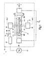
- Figure 1 shows a known piezoresistive MEMS resonator and it associated known drive and sense circuitry, and which is described in more detail in WO 2004/053431 .
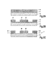
- Figure 2 shows the manufacturing process in simplified form.
- the resonator 1 shown in Fig. 1 comprises a substrate 10 which is a silicon wafer.
- substrate 10 may be a gallium arsenide wafer or it may comprise any other semiconducting, metal or dielectric material.
- resonators 1 designed for operation at frequencies above 10 MHz it is advantageous to use a substrate 10 comprising a dielectric, such as glass, because this reduces the loss of electromagnetic energy dissipated in the substrate.
- the resonator 1 further comprises an electrically conductive resonator element 20 having two parallel connecting elements 20a,20b.
- the resonator extends in a longitudinal direction having a length I, for operation in bulk mode. It is attached to the substrate 10 via support elements 21 and 22 which are connected to anchor elements 23 and 24, respectively.
- the anchor elements 23 and 24 are affixed to the substrate 10 (as is shown in Fig. 2C ).
- the resonator element 20 and the support elements 21 and 22 are free from the substrate 10 except for the connection via the anchor elements 23 and 24.
- the resonator may be manufactured using a technique well known in the field of micro electromechanical systems (MEMS).
- MEMS micro electromechanical systems
- the substrate 10 is first provided with an oxide layer 11 on top of which a silicon layer 12 is deposited, shown in Fig. 2A .
- the silicon layer 12 is covered by a photosensitive resist, not shown, which is patterned by, e.g. lithography.
- the patterned resist is then developed yielding the surface areas of the resonator element 20, the support elements 21 and 22, the anchor elements 23 and 24, and the actuator terminal 30 shown in Fig. 1 covered by the resist while the remaining part of the surface is free from resist.
- the surface partly covered by the resist is then subjected to etching which selectively removes those parts of the silicon layer 12 that are not covered by the resist. The result of the etching is shown in Fig. 2B . Subsequently, the oxide layer 11 which is exposed due to the previous etching is etched in a second etching step.
- This etching step removes all exposed parts of oxide layer 11 and, moreover, some of the oxide adjacent to these parts.
- the central parts of silicon layer 12 in Fig. 2C are free from the substrate. They form the resonator element 20.
- the oxide layer 11 under the support elements 21 and 22 is also removed such that the resonator element 20 is attached to the substrate 10 only via the anchor elements 23 and 24.
- the resonator element 20 has two outer ends 205 in the longitudinal direction. These can be larger than the combined width of the connecting beams 20a,20b and spacing 19 to define wider resonator masses at the ends, and thereby define a so-called dog-bone shape.
- Each of the outer ends 205 is faced by a respective electrode of the electrically conductive actuator 30, and is spaced from the electrode by an actuation gap g.
- the actuators can be considered to be gate terminals, in that the control input is applied to these terminals.
- the actuator 30 is able to receive an actuation potential difference V IN with respect to the resonator element 20 for elastically deforming the resonator element 20, using the electrostatic force.
- the actuation potential difference is a function of the input signal applied to the resonator 1.
- the actuation potential difference may typically further contain a DC component.
- the elastic deformation comprises a change of the length I by an amount dl shown in Fig. 1 .
- the resonator element 20 is part of an oscillator circuit which is able to conduct an electrical current through the resonator element 20.
- the resonator element 20 is electrically connected to the positive or negative pole of a DC voltage source V DC via an auxiliary resistor 27, the anchor element 24 and the support element 22.
- the anchor 24 can be considered to be a drain terminal in that the DC voltage bias is applied to this terminal to drive a bias current through the device.
- the resonator element 20 is further connected to ground via the support element 21 and the anchor element 23.
- the anchor 23 can be considered to be a source terminal in that the bias current is collected at this terminal. Therefore, the resonator element 20 is able to conduct an electrical current I. It constitutes a resistor with an ohmic resistance R which causes a voltage drop V when the resonator element 20 conducts the electrical current I.
- the resonator element 20 constitutes a resistor with an ohmic resistance R which is a function of the change dl of the length I because the resonator element 20 comprises a central part 19 with open space.
- the resonator element 20 comprises the two mutually parallel beams 20a,20b each of which is affixed to a respective support element 21 and 22. The two beams are connected with each other at the two outer ends by elements 205.
- the central part 19 has been created during the lithography step and the etching step described above. It prevents the current from flowing from the support element 22 to the support element 21 in a straight line. The current has to follow the conductive path formed by the resonator element 20. This conductive path extends in the longitudinal direction.
- the circuit is able to produce an output signal which is a function of the change dl of the length I and which is a function of the resistance R.
- the circuit comprises a measurement point 28 which is electrically connected to the circuit. It is situated between the auxiliary resistor 27 and the anchor element 24, and in operation it produces an electrical output signal which is the electrical potential difference Vout between the measurement point 28 and the reference point 29 which is connected to ground.
- the DC bias circuit and the output voltage measurement circuit are independent, and each consumes electrical power. More generally, separate currents required for each system block, such as the resonator-biasing circuit, amplifier circuitry of the output measurement circuitry, and also temperature control circuitry for providing temperature compensation. These currents increase the total power consumption.
- the resonator properties can usually not be completely optimized to fully use the available supply voltage, resulting in an additional power demand to accommodate the unused amount of headroom.
- the invention provides an arrangement in which the DC bias circuit and the measurement circuit are designed as a combined circuit so as to reduce power consumption.
- the current flowing as a result of the DC voltage bias can be used as part of the voltage sensing function.
- the circuit design is based on stacked system blocks, effectively reusing current.
- a power control loop is also implemented to stabilize the resonator fluctuations, preventing frequency shifts of the oscillator frequency.
- Figure 3 shows a first example of circuit of the invention in schematic form, to illustrate the signal amplification principle.
- the piezoresistive resonator 20 is represented by a resistance R RES through which a current I RES flows as a result of the desired DC voltage bias.
- the amplifier is shown as an operational amplifier (opamp) 31 which has one input connected to a fixed DC voltage V FIXED at a bias terminal 34. Due to the opamp function the voltage V D on the other input terminal is constant as well.
- Fluctuations at the intended oscillation frequency are represented by a change in resistance ⁇ r of the resonator, and lead to varying of the output voltage V OUT at the output 32 of the opamp 31.
- V D is constant, so the change in resistance R RES by the amount ⁇ r results in a change in the current flowing I RES .
- This current can only flow through a negative feedback resistor R FB of the opamp, so the fluctuations in R RES result in a fluctuation of V OUT .
- the amplifier circuit controls the voltage across the resonator body by holding the resonator body to the voltage V D .
- a current path is provided between the output of the amplifier (V OUT ) and the resonator body 20 such that changes in current through the resonator body 20, resulting from changes in resistance of the resonator body ⁇ r, result in a change in current flow I RES at the amplifier output.
- This change in current flow is detectable, either as a current signal or a voltage level, in order to derive the oscillation signal.
- Figure 3 shows an opamp.
- the circuit of the invention can be implemented with a simpler amplifier design.
- Figure 4 shows a configuration which uses a single MOS transistor, in common gate configuration, as the amplifier.
- the same function can be implemented with a common base bipolar implementation.
- This transistor functions in the general manner explained with reference to Figure 3 , as outlined below.
- the transistor 40 is in series between the supply voltage V SUPPLY and the resonator 20.
- the actuation electrode 30 (otherwise termed "gate electrode") of the resonator 20 has an AC input voltage IN applied in known manner.
- a bias voltage V BIAS is applied to the gate 41 of the transistor.
- the DC source voltage is determined by the threshold voltage of the transistor, and the resulting voltage applied to the bias electrode 44 corresponds to the voltage V D in Figure 3 .
- the current source 46 shown in Figure 4 represents an active load of the common gate amplifier circuit.
- the bias current generated by the active load I BIAS flows through the resonator, and this therefore dictates the voltage at the bias electrode 44 which is a function of the resonator resistance.
- the voltage at the transistor source is dependent on the resonator resistance, and is therefore modulated by the resonator oscillation.
- the common gate transistor functions as a current buffer or as a voltage amplifier for the AC signal variations, in known manner, and the output at output terminal 43 can be an output voltage or a current.
- the output is essentially the transistor drain, and there is a current path from the transistor drain to the resonator, through the transistor. This current defines the DC operating point of the transistor. There is no current flow to/from the actual output (if voltage sensing is used); the current flow is sourced from the supply).
- the amplifier circuit of Figure 3 forces the voltage applied to the resonator V D to be fixed (equal to V FIXED ) and in Figure 4 the voltage is not directly controlled but is the result of the currents flowing.
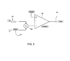
- Figure 5 shows an error amplifier 50 which is used to vary the level V FIXED to provide a power control function.
- V FIXED is selected to represent the desired amount of dissipated power in the resonator body, and can thus be used as a control parameter.
- This control loop is designed such that it can not change too fast, and in particular is at least several orders of magnitude slower than the oscillator frequency. The resonator power can then be controlled and stabilized.
- V FIXED is not always constant but might be related to other parameters for realization of an adaptive system.
- a possible example can be a relation to a temperature-sensor, on-chip or otherwise, for incorporating the ambient temperature and/or dissipation into the power-level to which the resonator-power is stabilized.
- the slow feedback loop consists of a sensor for determining the current through the resonator I RES and the voltage across the resonator V D .
- a current sensing resistor 52 of value R SENSE is provided as well as a voltage sensing circuit 54.
- a multiplier 56 generates the value I RES * V D , and the opamp 50 enforces the equality of the desired resonator power V POWER supplied to one terminal of the opamp 50, and the measured resonator power supplied by the multiplier 56 to the other opamp terminal.
- the opamp 50 generates the value V FIXED , which is no longer totally fixed but an intermediate but slowly changing variable voltage to provide power control.
- the power control and signal amplification share resources.
- Two control loops are simultaneously in operation.
- a fast loop implements the signal amplification and a slow loop implements the stabilisation of the resonator power.
- This slow loop essentially varies the DC bias of the amplifier circuit.
- the slow control loop will result in a change in the voltage V BIAS at the gat 41.
- resonator circuit of the invention Only one design of resonator has been shown. However, the invention can be applied to other resonator designs. Any resonator in which the resonator oscillation results in a change in resistance which needs to be measured can be used in the oscillator circuit of the invention.
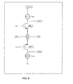
- Figure 6 shows an example of resonator with two separate gates, and which is in series between two complementary transistors MN-1 and MP-1. These together function as the amplifier, and they form a virtual earth input for the resonator, and use the same DC current.
- the series-connected components are biased by current sources I BIAS .
- Figure 7 shows an example of oscillator circuit based on the resonator design of Figure 6 .
- the oscillator circuit is implemented by closed loop connections to the resonator gates.
- Figure 8 shows a circuit equivalent to Figure 6 but based on complementary bipolar transistors QNPN-1 and QPNP-1.
- Figure 9 shows a variation to the circuit of Figure 6 in which resistors are used instead of current sources.
- Figure 10 shows how the schematic circuit of Figure 3 can be implemented at transistor level.
- the series connection of the output transistor MP1, the feedback resistor R FB and the resonator is shown. Thjs forms an output branch. This part of the circuit carries the most current, so that the current re-use in the output branch provides significant power savings, even though the input branch is not stacked above the resonator.
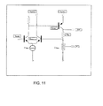
- Figure 11 shows a circuit equivalent to Figure 10 but based on bipolar transistors.
- amplifier circuits can be used. Thus, op-amps can be used, but other simpler amplifier circuits can also be used, as is clear from the examples above.
- op-amps can be used, but other simpler amplifier circuits can also be used, as is clear from the examples above.
Landscapes
- Physics & Mathematics (AREA)
- Acoustics & Sound (AREA)
- Oscillators With Electromechanical Resonators (AREA)
Abstract
Description
- This invention relates to MEMS oscillators, for example for generating clock signals or reference frequency signals.
- Electronic components inside flat objects, such as tags, bank cards or ID cards require a low profile of typically less than 0.5 mm. It is anticipated that flat, low-cost, and low power real time clocks (RTCs) and frequency reference oscillators (RFOs) are required residing inside these flat objects for future applications in the e-security, pharmaceutical, and food industry. An oscillator comprises a resonator and a feedback amplifier circuit, which are connected in a closed feedback loop. State-of-the-art RTCs make use of quartz crystal resonators with a height profile that typically exceeds the allowed sub-mm specification needed for their incorporation into flat products like cards, tags, and sheets of (value) paper. The main reason for this is because the packaging technology being used to encapsulate the quartz crystal does not lend itself well to miniaturization.
- Furthermore, quartz resonators cannot be integrated easily on a Si chip. Therefore, the integration of a complete oscillator consisting of the crystal and amplifier cannot be realized on a single chip and further prohibits the miniaturization of RTCs and RFOs. In contrast, a MEMS resonator can be processed and packaged using surface micro-machining techniques and can be integrated with the amplifier circuit to form a very small form-factor oscillator.
- Surface micro-machining is a technique whereby freestanding and moveable structures are made on top of a substrate using thin film deposition and etching techniques. In this way, both the resonator and its package can be processed on top of e.g. a Si wafer. The packaged resonator has a height of only several thin films measuring about 10 µm in total thickness. Furthermore, surface micro-machining allows for the definition of many thousands of packaged resonators onto a single wafer without making use of expensive assembly steps. The production cost associated with micro-machining decreases when the area occupied by a single device decreases. In this way, miniaturization of the resonator also has cost advantages. For quartz resonators, the production cost increases when the size of the resonator decreases as a result of the assembly-like production process that is being used.
- MEMS-resonator based oscillators thus allow for low profile and low cost clocks and oscillators. However, they do not necessarily consume little power. Piezoresistive MEMS resonators require a body DC bias-current and a DC polarization voltage for their electrode. The body of a piezoresistive resonator is fed a DC-current. By applying an AC-signal to an attached but isolated electrode ('gate') the resistivity of the body is modulated, so a signal voltage develops. This takes place in a narrow frequency region for proper operation.
- The various current paths can result in significant power consumption.
- According to the invention, there is provided a piezoresistive MEMS oscillator comprising:
- a resonator body;
- at least one drive electrode located adjacent the resonator body for providing an actuation signal;
- at least one bias electrode for supplying a bias current to the resonator body;
- an output circuit for generating an output which is a function of changes in resistance of the resonator body,
- This arrangement uses the bias current flowing through the resonator to play a role in deriving the circuit output. In this way, the same current is used to provide the required DC resonator bias and to drive the output circuit at its DC operating point and generate the output. The current path between the output of the output circuit and the resonator body can include other components (such as resistors or transistors). However, there is a path between the output and the resonator so that the resonator DC bias current (or a fraction of it) can flow in operation between the output and the resonator. The actual current is not necessarily sourced from the output - it may be sourced from the voltage supply. The current path however includes one or more components of the output circuit and thereby plays a role in defining the output circuit operating point. Thus, the output stage and the resonator are not separate isolated circuit units, but they are instead interconnected by a current path which means that the DC bias which sets the DC operating point of each has a shared current component.
- By using the same current for both the resonator-biasing as well as for the biasing of the output circuit (i.e. the readout interface), a MEMS-based oscillator with a lower total power consumption can be realized.
- The output circuit can comprise part of an amplifier circuit, or indeed it may comprise the complete amplifier circuit (if the amplifier circuit is designed with a single stage).
- Preferably, the output circuit and the resonator body are in series between power supply rails. Thus, the current flow across the output circuit is the same as the current flow through the resonator.
- An active load can be used to supply current to the series connection of the output circuit and resonator. The output circuit preferably comprises a DC bias terminal for setting a DC bias of the amplifier circuit.
- In one example, the output circuit comprises an amplifier circuit with a transistor (common gate or common base) in series with the resonator body, with a DC bias applied to the DC bias terminal, and the DC bias terminal comprises the gate or base. This provides a particularly simple circuit implementation with a current source (the active load) and a single transistor functioning as the amplifier circuit. The output of the amplifier circuit is then at the drain or collector of the transistor.
- In another example, the output circuit comprises an amplifier circuit which comprises first and second transistors in series with the resonator body and on opposite sides of the resonator body, with a DC bias applied to two DC bias terminals which comprise the gates or bases of the first and second transistors.
- This enables the resonator terminals to be virtual earth terminals, which gives reduced sensitivity to unwanted capacitances.
- In one arrangement, a fixed voltage is applied to the DC bias terminal or terminals. This causes the amplifier to hold the resonator to a fixed voltage so that changes in resonator current couple to the amplifier circuit output by the current path provided.
- However, in another arrangement, a variable voltage is applied to the DC bias terminal or terminals, wherein the variable voltage is selected to provide a desired power dissipation in the resonator body. In this way, the DC bias point of the amplifier circuit is used as a power control parameter.
- A circuit can be provided for sensing the electrical power dissipation in the resonator body, and a circuit is then provided for comparing the sensed electrical power dissipation with a desired power dissipation and deriving from the comparison the signal for the DC bias terminal to obtain the desired electrical power dissipation. A current sensor, a voltage sensor and a multiplier can be used. The variable voltage preferably fluctuates more slowly than the output of the amplifier circuit, and thus a slow feedback control loop is implemented for power control, compared to the resonator oscillation.
- The invention also provides a method of controlling a piezoresistive MEMS oscillator comprising:
- providing an actuation signal to a resonator body;
- supplying a bias current to the resonator body;
- generating an output which is a function of changes in resistance of the resonator body using an output circuit,
- wherein the method comprises:
- using the output circuit to control the voltage across or current through the resonator body; and
- providing a current path between the output of the output circuit and the resonator body.
- In this method, changes in current through or voltage across the resonator body, resulting from changes in resistance of the resonator body, result in a change in current flow or voltage at the output.
- Examples of the invention will now be described with reference to the accompanying drawings, in which:
-
Figure 1 shows a known piezoresistive MEMS resonator and biasing details; -
Figure 2 shows in simplified form how the resonator ofFigure 1 is manufactured; -
Figure 3 shows a first example of oscillator circuit of the invention in schematic form; -
Figure 4 shows an example of implementation of the circuit ofFigure 3 ; -
Figure 5 shows an additional power control circuit which can be combined with the circuit ofFigure 3 or Figure 4 ; and -
Figures 6 to 11 show various alternative resonator and oscillator circuit designs which operate using the same principles. - The invention provides a piezoresistive MEMS oscillator in which an output circuit circuit controls the voltage across the resonator body, and this results in a DC bias of the resonator. A current path is provided between the output of the output circuit (i.e. the output of the oscillator) and the resonator body such that changes in current through the resonator body, resulting from changes in resistance of the resonator body, are coupled to the output. This arrangement uses the bias current flowing through the resonator to derive the output. In this way, the same current is used to provide the required DC resonator bias and to control the output circuit.
- The output circuit can comprise an amplifier, or it can comprise the output stage of a multiple-stage amplifier circuit, .Preferably, the output circuit is a part of the oscillator circuit with a relatively large current consumption, so that power savings are obtained by reusing the bias current of the output stage to form the resonator bias current.
- The invention can be applied to any known oscillator circuit using a piezoresistive resonator. To explain the drive and sensing signals needed, a single example of resonator will be described.
Figure 1 shows a known piezoresistive MEMS resonator and it associated known drive and sense circuitry, and which is described in more detail inWO 2004/053431 .Figure 2 shows the manufacturing process in simplified form. - The
resonator 1 shown inFig. 1 comprises asubstrate 10 which is a silicon wafer. Alternatively,substrate 10 may be a gallium arsenide wafer or it may comprise any other semiconducting, metal or dielectric material. Forresonators 1 designed for operation at frequencies above 10 MHz it is advantageous to use asubstrate 10 comprising a dielectric, such as glass, because this reduces the loss of electromagnetic energy dissipated in the substrate. - The
resonator 1 further comprises an electricallyconductive resonator element 20 having two parallel connectingelements substrate 10 viasupport elements elements anchor elements Fig. 2C ). Theresonator element 20 and thesupport elements substrate 10 except for the connection via theanchor elements - The resonator may be manufactured using a technique well known in the field of micro electromechanical systems (MEMS). In short, the
substrate 10 is first provided with anoxide layer 11 on top of which asilicon layer 12 is deposited, shown inFig. 2A . - The
silicon layer 12 is covered by a photosensitive resist, not shown, which is patterned by, e.g. lithography. The patterned resist is then developed yielding the surface areas of theresonator element 20, thesupport elements anchor elements actuator terminal 30 shown inFig. 1 covered by the resist while the remaining part of the surface is free from resist. The surface partly covered by the resist is then subjected to etching which selectively removes those parts of thesilicon layer 12 that are not covered by the resist. The result of the etching is shown inFig. 2B . Subsequently, theoxide layer 11 which is exposed due to the previous etching is etched in a second etching step. This etching step removes all exposed parts ofoxide layer 11 and, moreover, some of the oxide adjacent to these parts. As a result of the second etching step, the central parts ofsilicon layer 12 inFig. 2C are free from the substrate. They form theresonator element 20. At the same etching step, theoxide layer 11 under thesupport elements resonator element 20 is attached to thesubstrate 10 only via theanchor elements - The
resonator element 20 has twoouter ends 205 in the longitudinal direction. These can be larger than the combined width of the connectingbeams - Each of the outer ends 205 is faced by a respective electrode of the electrically
conductive actuator 30, and is spaced from the electrode by an actuation gap g. The actuators can be considered to be gate terminals, in that the control input is applied to these terminals. Theactuator 30 is able to receive an actuation potential difference VIN with respect to theresonator element 20 for elastically deforming theresonator element 20, using the electrostatic force. The actuation potential difference is a function of the input signal applied to theresonator 1. In addition to the input signal the actuation potential difference may typically further contain a DC component. The elastic deformation comprises a change of the length I by an amount dl shown inFig. 1 . - The
resonator element 20 is part of an oscillator circuit which is able to conduct an electrical current through theresonator element 20. - In the known circuit configuration of
Figure 1 , theresonator element 20 is electrically connected to the positive or negative pole of a DC voltage source VDC via anauxiliary resistor 27, theanchor element 24 and thesupport element 22. Theanchor 24 can be considered to be a drain terminal in that the DC voltage bias is applied to this terminal to drive a bias current through the device. Theresonator element 20 is further connected to ground via thesupport element 21 and theanchor element 23. Theanchor 23 can be considered to be a source terminal in that the bias current is collected at this terminal. Therefore, theresonator element 20 is able to conduct an electrical current I. It constitutes a resistor with an ohmic resistance R which causes a voltage drop V when theresonator element 20 conducts the electrical current I. - The
resonator element 20 constitutes a resistor with an ohmic resistance R which is a function of the change dl of the length I because theresonator element 20 comprises acentral part 19 with open space. Theresonator element 20 comprises the two mutuallyparallel beams respective support element elements 205. Thecentral part 19 has been created during the lithography step and the etching step described above. It prevents the current from flowing from thesupport element 22 to thesupport element 21 in a straight line. The current has to follow the conductive path formed by theresonator element 20. This conductive path extends in the longitudinal direction. - The circuit is able to produce an output signal which is a function of the change dl of the length I and which is a function of the resistance R. To this end the circuit comprises a
measurement point 28 which is electrically connected to the circuit. It is situated between theauxiliary resistor 27 and theanchor element 24, and in operation it produces an electrical output signal which is the electrical potential difference Vout between themeasurement point 28 and thereference point 29 which is connected to ground. - In this arrangement, the DC bias circuit and the output voltage measurement circuit are independent, and each consumes electrical power. More generally, separate currents required for each system block, such as the resonator-biasing circuit, amplifier circuitry of the output measurement circuitry, and also temperature control circuitry for providing temperature compensation. These currents increase the total power consumption. In addition, the resonator properties can usually not be completely optimized to fully use the available supply voltage, resulting in an additional power demand to accommodate the unused amount of headroom.
- The invention provides an arrangement in which the DC bias circuit and the measurement circuit are designed as a combined circuit so as to reduce power consumption. In particular, the current flowing as a result of the DC voltage bias can be used as part of the voltage sensing function.
- The circuit design is based on stacked system blocks, effectively reusing current. In a preferred implementation, a power control loop is also implemented to stabilize the resonator fluctuations, preventing frequency shifts of the oscillator frequency.
-
Figure 3 shows a first example of circuit of the invention in schematic form, to illustrate the signal amplification principle. - The
piezoresistive resonator 20 is represented by a resistance RRES through which a current IRES flows as a result of the desired DC voltage bias. The amplifier is shown as an operational amplifier (opamp) 31 which has one input connected to a fixed DC voltage VFIXED at abias terminal 34. Due to the opamp function the voltage VD on the other input terminal is constant as well. - Fluctuations at the intended oscillation frequency are represented by a change in resistance Δr of the resonator, and lead to varying of the output voltage VOUT at the
output 32 of theopamp 31. VD is constant, so the change in resistance RRES by the amount Δr results in a change in the current flowing IRES. This current can only flow through a negative feedback resistor RFB of the opamp, so the fluctuations in RRES result in a fluctuation of VOUT. - Thus, the amplifier circuit controls the voltage across the resonator body by holding the resonator body to the voltage VD. A current path is provided between the output of the amplifier (VOUT) and the
resonator body 20 such that changes in current through theresonator body 20, resulting from changes in resistance of the resonator body Δr, result in a change in current flow IRES at the amplifier output. This change in current flow is detectable, either as a current signal or a voltage level, in order to derive the oscillation signal. - It can be seen that this design reuses current flow, in that the current path between the resonator and the output (which in this schematic example is the negative feedback path) results in the same current being used for DC biasing the
resonator 20 as for constructing the output signal. - In addition, as a result of the virtual-earth for the resonator to amplifier connection of the circuit of
Figure 3 , a reduced sensitivity for bond pad and other stray capacitances is obtained. -
Figure 3 shows an opamp. However, the circuit of the invention can be implemented with a simpler amplifier design. -
Figure 4 shows a configuration which uses a single MOS transistor, in common gate configuration, as the amplifier. Of course, the same function can be implemented with a common base bipolar implementation. - This transistor functions in the general manner explained with reference to
Figure 3 , as outlined below. - The
transistor 40 is in series between the supply voltage VSUPPLY and theresonator 20. The actuation electrode 30 (otherwise termed "gate electrode") of theresonator 20 has an AC input voltage IN applied in known manner. - A bias voltage VBIAS is applied to the
gate 41 of the transistor. The DC source voltage is determined by the threshold voltage of the transistor, and the resulting voltage applied to thebias electrode 44 corresponds to the voltage VD inFigure 3 . - The
current source 46 shown inFigure 4 represents an active load of the common gate amplifier circuit. The bias current generated by the active load IBIAS flows through the resonator, and this therefore dictates the voltage at thebias electrode 44 which is a function of the resonator resistance. - The voltage at the transistor source is dependent on the resonator resistance, and is therefore modulated by the resonator oscillation. The common gate transistor functions as a current buffer or as a voltage amplifier for the AC signal variations, in known manner, and the output at
output terminal 43 can be an output voltage or a current. - The output is essentially the transistor drain, and there is a current path from the transistor drain to the resonator, through the transistor. This current defines the DC operating point of the transistor. There is no current flow to/from the actual output (if voltage sensing is used); the current flow is sourced from the supply).
- In order to prevent changes of the resonator frequency, it is known to apply a power control method. The approach of
Figures 3 and 4 can be supplemented with a power control circuit, as shown inFigure 5 . - The amplifier circuit of
Figure 3 forces the voltage applied to the resonator VD to be fixed (equal to VFIXED) and inFigure 4 the voltage is not directly controlled but is the result of the currents flowing. -
Figure 5 shows anerror amplifier 50 which is used to vary the level VFIXED to provide a power control function. - In particular, the value of VFIXED is selected to represent the desired amount of dissipated power in the resonator body, and can thus be used as a control parameter. This control loop is designed such that it can not change too fast, and in particular is at least several orders of magnitude slower than the oscillator frequency. The resonator power can then be controlled and stabilized.
- From a system point of view it may be desirable that the value of VFIXED is not always constant but might be related to other parameters for realization of an adaptive system. A possible example can be a relation to a temperature-sensor, on-chip or otherwise, for incorporating the ambient temperature and/or dissipation into the power-level to which the resonator-power is stabilized.
- The slow feedback loop consists of a sensor for determining the current through the resonator IRES and the voltage across the resonator VD. As shown, a
current sensing resistor 52 of value RSENSE is provided as well as avoltage sensing circuit 54. - A
multiplier 56 generates the value IRES * VD, and theopamp 50 enforces the equality of the desired resonator power VPOWER supplied to one terminal of theopamp 50, and the measured resonator power supplied by themultiplier 56 to the other opamp terminal. Theopamp 50 generates the value VFIXED, which is no longer totally fixed but an intermediate but slowly changing variable voltage to provide power control. - In the same way that the resonator current is used by the amplifier to generate the output signal, the power control and signal amplification share resources. Two control loops are simultaneously in operation. A fast loop implements the signal amplification and a slow loop implements the stabilisation of the resonator power. This slow loop essentially varies the DC bias of the amplifier circuit. For example, with reference to
Figure 4 , the slow control loop will result in a change in the voltage VBIAS at thegat 41. - Only one design of resonator has been shown. However, the invention can be applied to other resonator designs. Any resonator in which the resonator oscillation results in a change in resistance which needs to be measured can be used in the oscillator circuit of the invention.
- Various other designs are shown in
Figures 6 to 11 . -
Figure 6 shows an example of resonator with two separate gates, and which is in series between two complementary transistors MN-1 and MP-1. These together function as the amplifier, and they form a virtual earth input for the resonator, and use the same DC current. The series-connected components are biased by current sources IBIAS. - In this way, the advantage of a virtual earth connection to the resonator, as explained with reference to the opamp implementation of
Figure 3 , is obtained with a more simple circuit implementation. -
Figure 7 shows an example of oscillator circuit based on the resonator design ofFigure 6 . The oscillator circuit is implemented by closed loop connections to the resonator gates. -
Figure 8 shows a circuit equivalent toFigure 6 but based on complementary bipolar transistors QNPN-1 and QPNP-1. -
Figure 9 shows a variation to the circuit ofFigure 6 in which resistors are used instead of current sources. -
Figure 10 shows how the schematic circuit ofFigure 3 can be implemented at transistor level. - The series connection of the output transistor MP1, the feedback resistor RFB and the resonator is shown. Thjs forms an output branch. This part of the circuit carries the most current, so that the current re-use in the output branch provides significant power savings, even though the input branch is not stacked above the resonator.
-
Figure 11 shows a circuit equivalent toFigure 10 but based on bipolar transistors. - These examples show that many different circuit implementations can benefit from the invention.
- Numerous other amplifier circuits can be used. Thus, op-amps can be used, but other simpler amplifier circuits can also be used, as is clear from the examples above. By placing at least the output stage of the amplifier and resonator in series, the same current is used to bias the resonator and to provide the required current flow through the output stage of the amplifier circuit to generate the output.
- Other variations to the disclosed embodiments can be understood and effected by those skilled in the art in practicing the claimed invention, from a study of the drawings, the disclosure, and the appended claims. In the claims, the word "comprising" does not exclude other elements or steps, and the indefinite article "a" or "an" does not exclude a plurality. The mere fact that certain measures are recited in mutually different dependent claims does not indicate that a combination of these measured cannot be used to advantage. Any reference signs in the claims should not be construed as limiting the scope.
Claims (15)
- A piezoresistive MEMS oscillator comprising:a resonator body (20);at least one drive electrode (30) located adjacent the resonator body for providing an actuation signal;at least one bias electrode (44) for supplying a bias current to the resonator body;an output circuit (31;40) for generating an output which is a function of changes in resistance of the resonator body (20),wherein the output circuit (31;40) controls the voltage across or current through the resonator body (20), wherein a current path is provided between the output (32;43) of the output circuit (31;40) and the resonator body (20), and wherein changes in current through the resonator body (20) or voltage across the resonator body, resulting from changes in resistance of the resonator body, result in a change in current flow or voltage at the amplifier output.
- An oscillator as claimed in claim 1, wherein the output circuit and the resonator body are in series between power supply rails.
- An oscillator as claimed in claim 1 or 2, further comprising an active load supplying current to the series connection of the output circuit (31 ;40) and resonator (20).
- An oscillator as claimed in any preceding claim, wherein the output circuit comprises a DC bias terminal (34;41) for setting a DC bias of the output circuit and thereby the DC bias current in the resonator (20).
- An oscillator as claimed in claim 4, wherein the output circuit comprises an amplifier circuit which comprises:a transistor (40) in series with the resonator body (20), with a DC bias (VBIAS) applied to the DC bias terminal (41), and the DC bias terminal (41) comprises the gate or base; orfirst and second transistors in series with the resonator body and on opposite sides of the resonator body, with a DC bias (VBIAS1, VBIAS2) applied to two DC bias terminals which comprise the gates or bases of the first and second transistors.
- An oscillator as claimed in claim 5, with the output (43) or outputs of the amplifier circuit at the drain or collector of the transistor or transistors.
- An oscillator as claimed in claim 4, 5 or 6, wherein a fixed voltage is applied to the DC bias terminal (34;41) or terminals.
- An oscillator as claimed in claim 4, 5 or 6, wherein a variable voltage is applied to the DC bias terminal (34;41) or terminals, wherein the variable voltage is selected to provide a desired power dissipation in the resonator body.
- An oscillator as claimed in claim 8, comprising a circuit (52,54) for sensing the electrical power dissipation in the resonator body, a circuit (50) for comparing the sensed electrical power dissipation with a desired power dissipation and deriving from the comparison the signal for the DC bias terminal (34;41) or terminals to obtain the desired electrical power dissipation.
- An oscillator as claimed in claim 9, wherein the circuit (52,54) for sensing the electrical power dissipation comprises a current sensor (52) and a voltage sensor (54) and a multiplier (56).
- An oscillator as claimed in claim 8, 9 or 10, wherein the variable voltage fluctuates more slowly than the output of the amplifier circuit (31 ;40).
- A method of controlling a piezoresistive MEMS oscillator comprising:providing an actuation signal to a resonator body;supplying a bias current to the resonator body;generating an output which is a function of changes in resistance of the resonator body using an output circuit (31 ;40),wherein the method comprises:using the output circuit (31,40) to control the voltage across or current through the resonator body (20); andproviding a current path between the output (32;43) of the output circuit and the resonator body (20).
- A method as claimed in claim 12, comprising applying a voltage to a DC bias terminal (34;41) of the output circuit (31,40) for setting a DC bias of the output circuit.
- A method as claimed in claim 13, wherein a variable voltage is applied to the DC bias terminal (34;41), wherein the variable voltage is selected to provide a desired power dissipation in the resonator body.
- A method as claimed in claim 14, comprising:sensing the electrical power dissipation in the resonator body (20);comparing the sensed electrical power dissipation with a desired power dissipation and deriving from the comparison the signal for the DC bias terminal (34;41) to obtain the desired electrical power dissipation.
Priority Applications (3)
| Application Number | Priority Date | Filing Date | Title |
|---|---|---|---|
| EP10187296.8A EP2442445B1 (en) | 2010-10-12 | 2010-10-12 | MEMS oscillator |
| CN201110304272.7A CN102447447B (en) | 2010-10-12 | 2011-10-10 | Mems oscillator |
| US13/271,970 US8564377B2 (en) | 2010-10-12 | 2011-10-12 | MEMS oscillator |
Applications Claiming Priority (1)
| Application Number | Priority Date | Filing Date | Title |
|---|---|---|---|
| EP10187296.8A EP2442445B1 (en) | 2010-10-12 | 2010-10-12 | MEMS oscillator |
Publications (2)
| Publication Number | Publication Date |
|---|---|
| EP2442445A1 true EP2442445A1 (en) | 2012-04-18 |
| EP2442445B1 EP2442445B1 (en) | 2013-12-11 |
Family
ID=43662039
Family Applications (1)
| Application Number | Title | Priority Date | Filing Date |
|---|---|---|---|
| EP10187296.8A Not-in-force EP2442445B1 (en) | 2010-10-12 | 2010-10-12 | MEMS oscillator |
Country Status (3)
| Country | Link |
|---|---|
| US (1) | US8564377B2 (en) |
| EP (1) | EP2442445B1 (en) |
| CN (1) | CN102447447B (en) |
Citations (4)
| Publication number | Priority date | Publication date | Assignee | Title |
|---|---|---|---|---|
| EP0959333A2 (en) * | 1998-05-22 | 1999-11-24 | Sumitomo Metal Industries Limited | Vibration wave detecting method and vibration wave detector |
| WO2004053431A2 (en) | 2002-12-10 | 2004-06-24 | Koninklijke Philips Electronics N.V. | Transducer and electronic device |
| WO2008149298A1 (en) * | 2007-06-04 | 2008-12-11 | Nxp B.V. | Pressure gauge |
| US20100219895A1 (en) * | 2009-02-27 | 2010-09-02 | Commissariat A L'energie Atomique | Transistor-based micrometric or nanometric resonant device |
Family Cites Families (5)
| Publication number | Priority date | Publication date | Assignee | Title |
|---|---|---|---|---|
| US8183946B2 (en) * | 2004-12-22 | 2012-05-22 | Nxp B.V. | Charge biased MEM resonator |
| DE102005058192A1 (en) * | 2005-12-06 | 2007-06-28 | Airbus Deutschland Gmbh | Device for fault detection of adjustable flaps |
| US20070257728A1 (en) * | 2006-05-03 | 2007-11-08 | Sitime Corporation | Microelectromechanical multi-stage oscillator |
| JP2009200888A (en) * | 2008-02-22 | 2009-09-03 | Seiko Instruments Inc | Mems oscillator |
| WO2010073213A2 (en) * | 2008-12-23 | 2010-07-01 | Nxp B.V. | Circuit for compensating influence of temperature on a resonator |
-
2010
- 2010-10-12 EP EP10187296.8A patent/EP2442445B1/en not_active Not-in-force
-
2011
- 2011-10-10 CN CN201110304272.7A patent/CN102447447B/en not_active Expired - Fee Related
- 2011-10-12 US US13/271,970 patent/US8564377B2/en active Active
Patent Citations (4)
| Publication number | Priority date | Publication date | Assignee | Title |
|---|---|---|---|---|
| EP0959333A2 (en) * | 1998-05-22 | 1999-11-24 | Sumitomo Metal Industries Limited | Vibration wave detecting method and vibration wave detector |
| WO2004053431A2 (en) | 2002-12-10 | 2004-06-24 | Koninklijke Philips Electronics N.V. | Transducer and electronic device |
| WO2008149298A1 (en) * | 2007-06-04 | 2008-12-11 | Nxp B.V. | Pressure gauge |
| US20100219895A1 (en) * | 2009-02-27 | 2010-09-02 | Commissariat A L'energie Atomique | Transistor-based micrometric or nanometric resonant device |
Non-Patent Citations (1)
| Title |
|---|
| BONTEMPS J J M ET AL: "56 MHZ piezoresistive micromechanical oscillator", SOLID-STATE SENSORS, ACTUATORS AND MICROSYSTEMS CONFERENCE, 2009. TRANSDUCERS 2009. INTERNATIONAL, IEEE, PISCATAWAY, NJ, USA, 21 June 2009 (2009-06-21), pages 1433 - 1436, XP031545723, ISBN: 978-1-4244-4190-7 * |
Also Published As
| Publication number | Publication date |
|---|---|
| EP2442445B1 (en) | 2013-12-11 |
| US8564377B2 (en) | 2013-10-22 |
| CN102447447B (en) | 2014-11-05 |
| US20120086514A1 (en) | 2012-04-12 |
| CN102447447A (en) | 2012-05-09 |
Similar Documents
| Publication | Publication Date | Title |
|---|---|---|
| US7616078B2 (en) | Device for controlling the frequency of resonance of an oscillating micro-electromechanical system | |
| US8461936B2 (en) | MEMS oscillator | |
| US7893781B2 (en) | Low-voltage MEMS oscillator | |
| Lavasani et al. | Electronic temperature compensation of lateral bulk acoustic resonator reference oscillators using enhanced series tuning technique | |
| WO2010052683A2 (en) | Mems resonator | |
| EP2382707A2 (en) | Circuit for compensating influence of temperature on a resonator | |
| EP3486629B1 (en) | Stress sensor | |
| EP2883307B1 (en) | Method and apparatus to control the lc tank temperature null characteristic in a highly stable lc oscillator | |
| JP2004144704A (en) | Inductance measuring method | |
| EP2442445B1 (en) | MEMS oscillator | |
| Do et al. | Design and implementation of a low-power hybrid capacitive MEMS oscillator | |
| JP5882392B2 (en) | Resonant device with improved characteristics | |
| US8902022B2 (en) | Resonator and method of controlling the same | |
| Asadi et al. | CMOS Closed-Loop Control of MEMS Varactors for Robust K a-Band Tunable Filters | |
| Phan et al. | High precision frequency synthesizer based on MEMS piezoresistive resonator | |
| CN104836572B (en) | Phase-locked loop with the varactor based on MEMS technology | |
| US20120268218A1 (en) | Vibration circuit | |
| US11722096B2 (en) | Oven controlled MEMS oscillator with multiple temperature control loops | |
| CN100578914C (en) | Varactor device with reduced temperature dependence | |
| CN102457228B (en) | Piezoelectric oscillation circuit and temperature-constant piezoelectric oscillator | |
| EP2224589A1 (en) | Oscillator circuit comprising a resistor element buffering a resonator output from peripheral loads | |
| CN120578258A (en) | Regulating circuit, circuit arrangement and oscillator | |
| JP2009004972A (en) | Semiconductor integrated circuit |
Legal Events
| Date | Code | Title | Description |
|---|---|---|---|
| PUAI | Public reference made under article 153(3) epc to a published international application that has entered the european phase |
Free format text: ORIGINAL CODE: 0009012 |
|
| AK | Designated contracting states |
Kind code of ref document: A1 Designated state(s): AL AT BE BG CH CY CZ DE DK EE ES FI FR GB GR HR HU IE IS IT LI LT LU LV MC MK MT NL NO PL PT RO RS SE SI SK SM TR |
|
| AX | Request for extension of the european patent |
Extension state: BA ME |
|
| 17P | Request for examination filed |
Effective date: 20121018 |
|
| RIC1 | Information provided on ipc code assigned before grant |
Ipc: H03B 5/36 20060101ALI20130328BHEP Ipc: H03H 9/02 20060101AFI20130328BHEP |
|
| GRAP | Despatch of communication of intention to grant a patent |
Free format text: ORIGINAL CODE: EPIDOSNIGR1 |
|
| INTG | Intention to grant announced |
Effective date: 20130507 |
|
| GRAS | Grant fee paid |
Free format text: ORIGINAL CODE: EPIDOSNIGR3 |
|
| GRAA | (expected) grant |
Free format text: ORIGINAL CODE: 0009210 |
|
| AK | Designated contracting states |
Kind code of ref document: B1 Designated state(s): AL AT BE BG CH CY CZ DE DK EE ES FI FR GB GR HR HU IE IS IT LI LT LU LV MC MK MT NL NO PL PT RO RS SE SI SK SM TR |
|
| REG | Reference to a national code |
Ref country code: GB Ref legal event code: FG4D |
|
| REG | Reference to a national code |
Ref country code: CH Ref legal event code: EP |
|
| REG | Reference to a national code |
Ref country code: AT Ref legal event code: REF Ref document number: 645028 Country of ref document: AT Kind code of ref document: T Effective date: 20140115 |
|
| REG | Reference to a national code |
Ref country code: IE Ref legal event code: FG4D |
|
| REG | Reference to a national code |
Ref country code: DE Ref legal event code: R096 Ref document number: 602010012314 Country of ref document: DE Effective date: 20140206 |
|
| REG | Reference to a national code |
Ref country code: NL Ref legal event code: VDEP Effective date: 20131211 |
|
| REG | Reference to a national code |
Ref country code: AT Ref legal event code: MK05 Ref document number: 645028 Country of ref document: AT Kind code of ref document: T Effective date: 20131211 |
|
| PG25 | Lapsed in a contracting state [announced via postgrant information from national office to epo] |
Ref country code: NO Free format text: LAPSE BECAUSE OF FAILURE TO SUBMIT A TRANSLATION OF THE DESCRIPTION OR TO PAY THE FEE WITHIN THE PRESCRIBED TIME-LIMIT Effective date: 20140311 Ref country code: HR Free format text: LAPSE BECAUSE OF FAILURE TO SUBMIT A TRANSLATION OF THE DESCRIPTION OR TO PAY THE FEE WITHIN THE PRESCRIBED TIME-LIMIT Effective date: 20131211 Ref country code: FI Free format text: LAPSE BECAUSE OF FAILURE TO SUBMIT A TRANSLATION OF THE DESCRIPTION OR TO PAY THE FEE WITHIN THE PRESCRIBED TIME-LIMIT Effective date: 20131211 Ref country code: SE Free format text: LAPSE BECAUSE OF FAILURE TO SUBMIT A TRANSLATION OF THE DESCRIPTION OR TO PAY THE FEE WITHIN THE PRESCRIBED TIME-LIMIT Effective date: 20131211 Ref country code: LT Free format text: LAPSE BECAUSE OF FAILURE TO SUBMIT A TRANSLATION OF THE DESCRIPTION OR TO PAY THE FEE WITHIN THE PRESCRIBED TIME-LIMIT Effective date: 20131211 Ref country code: NL Free format text: LAPSE BECAUSE OF FAILURE TO SUBMIT A TRANSLATION OF THE DESCRIPTION OR TO PAY THE FEE WITHIN THE PRESCRIBED TIME-LIMIT Effective date: 20131211 |
|
| REG | Reference to a national code |
Ref country code: LT Ref legal event code: MG4D |
|
| PG25 | Lapsed in a contracting state [announced via postgrant information from national office to epo] |
Ref country code: CY Free format text: LAPSE BECAUSE OF FAILURE TO SUBMIT A TRANSLATION OF THE DESCRIPTION OR TO PAY THE FEE WITHIN THE PRESCRIBED TIME-LIMIT Effective date: 20131211 Ref country code: LV Free format text: LAPSE BECAUSE OF FAILURE TO SUBMIT A TRANSLATION OF THE DESCRIPTION OR TO PAY THE FEE WITHIN THE PRESCRIBED TIME-LIMIT Effective date: 20131211 Ref country code: AT Free format text: LAPSE BECAUSE OF FAILURE TO SUBMIT A TRANSLATION OF THE DESCRIPTION OR TO PAY THE FEE WITHIN THE PRESCRIBED TIME-LIMIT Effective date: 20131211 Ref country code: RS Free format text: LAPSE BECAUSE OF FAILURE TO SUBMIT A TRANSLATION OF THE DESCRIPTION OR TO PAY THE FEE WITHIN THE PRESCRIBED TIME-LIMIT Effective date: 20131211 |
|
| PG25 | Lapsed in a contracting state [announced via postgrant information from national office to epo] |
Ref country code: BE Free format text: LAPSE BECAUSE OF FAILURE TO SUBMIT A TRANSLATION OF THE DESCRIPTION OR TO PAY THE FEE WITHIN THE PRESCRIBED TIME-LIMIT Effective date: 20131211 Ref country code: EE Free format text: LAPSE BECAUSE OF FAILURE TO SUBMIT A TRANSLATION OF THE DESCRIPTION OR TO PAY THE FEE WITHIN THE PRESCRIBED TIME-LIMIT Effective date: 20131211 Ref country code: IS Free format text: LAPSE BECAUSE OF FAILURE TO SUBMIT A TRANSLATION OF THE DESCRIPTION OR TO PAY THE FEE WITHIN THE PRESCRIBED TIME-LIMIT Effective date: 20140411 |
|
| PG25 | Lapsed in a contracting state [announced via postgrant information from national office to epo] |
Ref country code: PT Free format text: LAPSE BECAUSE OF FAILURE TO SUBMIT A TRANSLATION OF THE DESCRIPTION OR TO PAY THE FEE WITHIN THE PRESCRIBED TIME-LIMIT Effective date: 20140411 Ref country code: CZ Free format text: LAPSE BECAUSE OF FAILURE TO SUBMIT A TRANSLATION OF THE DESCRIPTION OR TO PAY THE FEE WITHIN THE PRESCRIBED TIME-LIMIT Effective date: 20131211 Ref country code: RO Free format text: LAPSE BECAUSE OF FAILURE TO SUBMIT A TRANSLATION OF THE DESCRIPTION OR TO PAY THE FEE WITHIN THE PRESCRIBED TIME-LIMIT Effective date: 20131211 Ref country code: SK Free format text: LAPSE BECAUSE OF FAILURE TO SUBMIT A TRANSLATION OF THE DESCRIPTION OR TO PAY THE FEE WITHIN THE PRESCRIBED TIME-LIMIT Effective date: 20131211 Ref country code: ES Free format text: LAPSE BECAUSE OF FAILURE TO SUBMIT A TRANSLATION OF THE DESCRIPTION OR TO PAY THE FEE WITHIN THE PRESCRIBED TIME-LIMIT Effective date: 20131211 Ref country code: PL Free format text: LAPSE BECAUSE OF FAILURE TO SUBMIT A TRANSLATION OF THE DESCRIPTION OR TO PAY THE FEE WITHIN THE PRESCRIBED TIME-LIMIT Effective date: 20131211 |
|
| REG | Reference to a national code |
Ref country code: DE Ref legal event code: R097 Ref document number: 602010012314 Country of ref document: DE |
|
| PLBE | No opposition filed within time limit |
Free format text: ORIGINAL CODE: 0009261 |
|
| STAA | Information on the status of an ep patent application or granted ep patent |
Free format text: STATUS: NO OPPOSITION FILED WITHIN TIME LIMIT |
|
| PG25 | Lapsed in a contracting state [announced via postgrant information from national office to epo] |
Ref country code: DK Free format text: LAPSE BECAUSE OF FAILURE TO SUBMIT A TRANSLATION OF THE DESCRIPTION OR TO PAY THE FEE WITHIN THE PRESCRIBED TIME-LIMIT Effective date: 20131211 |
|
| 26N | No opposition filed |
Effective date: 20140912 |
|
| REG | Reference to a national code |
Ref country code: DE Ref legal event code: R097 Ref document number: 602010012314 Country of ref document: DE Effective date: 20140912 |
|
| PGFP | Annual fee paid to national office [announced via postgrant information from national office to epo] |
Ref country code: FR Payment date: 20141021 Year of fee payment: 5 Ref country code: DE Payment date: 20140924 Year of fee payment: 5 |
|
| PG25 | Lapsed in a contracting state [announced via postgrant information from national office to epo] |
Ref country code: SI Free format text: LAPSE BECAUSE OF FAILURE TO SUBMIT A TRANSLATION OF THE DESCRIPTION OR TO PAY THE FEE WITHIN THE PRESCRIBED TIME-LIMIT Effective date: 20131211 |
|
| PG25 | Lapsed in a contracting state [announced via postgrant information from national office to epo] |
Ref country code: MC Free format text: LAPSE BECAUSE OF FAILURE TO SUBMIT A TRANSLATION OF THE DESCRIPTION OR TO PAY THE FEE WITHIN THE PRESCRIBED TIME-LIMIT Effective date: 20131211 Ref country code: LU Free format text: LAPSE BECAUSE OF FAILURE TO SUBMIT A TRANSLATION OF THE DESCRIPTION OR TO PAY THE FEE WITHIN THE PRESCRIBED TIME-LIMIT Effective date: 20141012 |
|
| REG | Reference to a national code |
Ref country code: CH Ref legal event code: PL |
|
| GBPC | Gb: european patent ceased through non-payment of renewal fee |
Effective date: 20141012 |
|
| REG | Reference to a national code |
Ref country code: IE Ref legal event code: MM4A |
|
| PG25 | Lapsed in a contracting state [announced via postgrant information from national office to epo] |
Ref country code: CH Free format text: LAPSE BECAUSE OF NON-PAYMENT OF DUE FEES Effective date: 20141031 Ref country code: LI Free format text: LAPSE BECAUSE OF NON-PAYMENT OF DUE FEES Effective date: 20141031 Ref country code: GB Free format text: LAPSE BECAUSE OF NON-PAYMENT OF DUE FEES Effective date: 20141012 |
|
| PG25 | Lapsed in a contracting state [announced via postgrant information from national office to epo] |
Ref country code: IE Free format text: LAPSE BECAUSE OF NON-PAYMENT OF DUE FEES Effective date: 20141012 |
|
| PG25 | Lapsed in a contracting state [announced via postgrant information from national office to epo] |
Ref country code: SM Free format text: LAPSE BECAUSE OF FAILURE TO SUBMIT A TRANSLATION OF THE DESCRIPTION OR TO PAY THE FEE WITHIN THE PRESCRIBED TIME-LIMIT Effective date: 20131211 |
|
| REG | Reference to a national code |
Ref country code: DE Ref legal event code: R119 Ref document number: 602010012314 Country of ref document: DE |
|
| PG25 | Lapsed in a contracting state [announced via postgrant information from national office to epo] |
Ref country code: GR Free format text: LAPSE BECAUSE OF FAILURE TO SUBMIT A TRANSLATION OF THE DESCRIPTION OR TO PAY THE FEE WITHIN THE PRESCRIBED TIME-LIMIT Effective date: 20140312 Ref country code: IT Free format text: LAPSE BECAUSE OF FAILURE TO SUBMIT A TRANSLATION OF THE DESCRIPTION OR TO PAY THE FEE WITHIN THE PRESCRIBED TIME-LIMIT Effective date: 20131211 Ref country code: BG Free format text: LAPSE BECAUSE OF FAILURE TO SUBMIT A TRANSLATION OF THE DESCRIPTION OR TO PAY THE FEE WITHIN THE PRESCRIBED TIME-LIMIT Effective date: 20131211 |
|
| PG25 | Lapsed in a contracting state [announced via postgrant information from national office to epo] |
Ref country code: MT Free format text: LAPSE BECAUSE OF FAILURE TO SUBMIT A TRANSLATION OF THE DESCRIPTION OR TO PAY THE FEE WITHIN THE PRESCRIBED TIME-LIMIT Effective date: 20131211 Ref country code: DE Free format text: LAPSE BECAUSE OF NON-PAYMENT OF DUE FEES Effective date: 20160503 Ref country code: TR Free format text: LAPSE BECAUSE OF FAILURE TO SUBMIT A TRANSLATION OF THE DESCRIPTION OR TO PAY THE FEE WITHIN THE PRESCRIBED TIME-LIMIT Effective date: 20131211 Ref country code: HU Free format text: LAPSE BECAUSE OF FAILURE TO SUBMIT A TRANSLATION OF THE DESCRIPTION OR TO PAY THE FEE WITHIN THE PRESCRIBED TIME-LIMIT; INVALID AB INITIO Effective date: 20101012 |
|
| REG | Reference to a national code |
Ref country code: FR Ref legal event code: ST Effective date: 20160630 |
|
| PG25 | Lapsed in a contracting state [announced via postgrant information from national office to epo] |
Ref country code: FR Free format text: LAPSE BECAUSE OF NON-PAYMENT OF DUE FEES Effective date: 20151102 |
|
| PG25 | Lapsed in a contracting state [announced via postgrant information from national office to epo] |
Ref country code: MK Free format text: LAPSE BECAUSE OF FAILURE TO SUBMIT A TRANSLATION OF THE DESCRIPTION OR TO PAY THE FEE WITHIN THE PRESCRIBED TIME-LIMIT Effective date: 20131211 |
|
| PG25 | Lapsed in a contracting state [announced via postgrant information from national office to epo] |
Ref country code: AL Free format text: LAPSE BECAUSE OF FAILURE TO SUBMIT A TRANSLATION OF THE DESCRIPTION OR TO PAY THE FEE WITHIN THE PRESCRIBED TIME-LIMIT Effective date: 20131211 |