EP2442096A1 - Determination of electromagnetic properties of samples - Google Patents
Determination of electromagnetic properties of samples Download PDFInfo
- Publication number
- EP2442096A1 EP2442096A1 EP11184867A EP11184867A EP2442096A1 EP 2442096 A1 EP2442096 A1 EP 2442096A1 EP 11184867 A EP11184867 A EP 11184867A EP 11184867 A EP11184867 A EP 11184867A EP 2442096 A1 EP2442096 A1 EP 2442096A1
- Authority
- EP
- European Patent Office
- Prior art keywords
- input
- sample holder
- measurement device
- electromagnetic
- sample
- Prior art date
- Legal status (The legal status is an assumption and is not a legal conclusion. Google has not performed a legal analysis and makes no representation as to the accuracy of the status listed.)
- Granted
Links
- 238000005259 measurement Methods 0.000 claims abstract description 94
- 230000005670 electromagnetic radiation Effects 0.000 claims description 17
- 239000011358 absorbing material Substances 0.000 claims description 4
- 230000002452 interceptive effect Effects 0.000 claims description 3
- 238000012545 processing Methods 0.000 abstract description 3
- 239000000523 sample Substances 0.000 description 62
- 239000000463 material Substances 0.000 description 16
- OKTJSMMVPCPJKN-UHFFFAOYSA-N Carbon Chemical compound [C] OKTJSMMVPCPJKN-UHFFFAOYSA-N 0.000 description 14
- 238000000034 method Methods 0.000 description 11
- 230000005855 radiation Effects 0.000 description 9
- 229910021389 graphene Inorganic materials 0.000 description 6
- 238000003780 insertion Methods 0.000 description 5
- 230000037431 insertion Effects 0.000 description 5
- 239000002041 carbon nanotube Substances 0.000 description 4
- 230000035699 permeability Effects 0.000 description 4
- 230000004075 alteration Effects 0.000 description 3
- 230000005540 biological transmission Effects 0.000 description 3
- 229910052799 carbon Inorganic materials 0.000 description 3
- 229910021393 carbon nanotube Inorganic materials 0.000 description 3
- 239000000758 substrate Substances 0.000 description 3
- 239000006096 absorbing agent Substances 0.000 description 2
- 125000004429 atom Chemical group 0.000 description 2
- 229910002804 graphite Inorganic materials 0.000 description 2
- 239000010439 graphite Substances 0.000 description 2
- 239000010409 thin film Substances 0.000 description 2
- 229910001369 Brass Inorganic materials 0.000 description 1
- 239000004411 aluminium Substances 0.000 description 1
- XAGFODPZIPBFFR-UHFFFAOYSA-N aluminium Chemical compound [Al] XAGFODPZIPBFFR-UHFFFAOYSA-N 0.000 description 1
- 229910052782 aluminium Inorganic materials 0.000 description 1
- 239000010951 brass Substances 0.000 description 1
- 229910021387 carbon allotrope Inorganic materials 0.000 description 1
- 125000004432 carbon atom Chemical group C* 0.000 description 1
- 230000008878 coupling Effects 0.000 description 1
- 238000010168 coupling process Methods 0.000 description 1
- 238000005859 coupling reaction Methods 0.000 description 1
- 239000013078 crystal Substances 0.000 description 1
- 238000013461 design Methods 0.000 description 1
- 230000005672 electromagnetic field Effects 0.000 description 1
- 238000000605 extraction Methods 0.000 description 1
- 230000001788 irregular Effects 0.000 description 1
- 238000000691 measurement method Methods 0.000 description 1
- 239000002086 nanomaterial Substances 0.000 description 1
- 238000009659 non-destructive testing Methods 0.000 description 1
- 239000005022 packaging material Substances 0.000 description 1
- 238000005096 rolling process Methods 0.000 description 1
- 230000035945 sensitivity Effects 0.000 description 1
- 229910052710 silicon Inorganic materials 0.000 description 1
- 239000010703 silicon Substances 0.000 description 1
- 238000012360 testing method Methods 0.000 description 1
- 238000012546 transfer Methods 0.000 description 1
Images



Classifications
-
- G—PHYSICS
- G01—MEASURING; TESTING
- G01N—INVESTIGATING OR ANALYSING MATERIALS BY DETERMINING THEIR CHEMICAL OR PHYSICAL PROPERTIES
- G01N22/00—Investigating or analysing materials by the use of microwaves or radio waves, i.e. electromagnetic waves with a wavelength of one millimetre or more
Definitions
- the present invention relates to the determination of electromagnetic properties of samples, and is more particularly concerned with a system and method for determining such properties of small samples.
- US-A-4507602 describes a system for measuring the properties of a sample.
- the sample is positioned between two sectoral horns that are placed mouth-to-mouth with the sample therebetween.
- An input signal in the Ku band (12.4 to 18GHz) is supplied to the sample via one horn and the transmitted and reflected signals from the sample are received at respective horns.
- the transmitted and reflected signals are analysed to determine the complex permittivity and permeability of the sample.
- Fabry-Perot resonators are also known for measuring the electromagnetic properties of samples using microwaves as described in " Fabry-Perot and Open Resonators at Microwave and Millimetre Wave Frequencies, 2-300GTHz", J. Phys. E: Sci. Instrum., Vol. 15, 1982 . Properties that can be measured include dielectric constant, anisotropy, and magnetic resonance.
- Corrugated horn antennas can be used with elliptical surfaces for measuring laminar samples as described by J Krupka in "Frequency Domain Complex Permittivity Measurements at Microwave Frequencies", Meas. Sci. Technol., Vol. 17, pages 55 to 70, 2006 .
- the methods require a three-dimensional measurement to be made of the small sample and correct alignment of the sample in three dimensions is required to have good measurement results.
- Microwave energy is coupled to a measurement chamber via a coaxial transmission line over a multi-octave bandwidth via an intermediate microstrip-to-slotline coupling circuit.
- a measurement device (100; 200; 400; 500) for measuring electromagnetic characteristics of at least sub-millimetre sized samples using electromagnetic radiation, the measurement device comprising:-
- the focal points can be used for positioning the sample holder, and hence, the sample to be tested as well as the input/output ports. This provides an efficient transfer of electromagnetic energy to and from the sample in the sample holder.
- the partly conic shape comprises an ellipse and the reflective surface comprises a portion of the ellipse.
- a single reflective surface is provided that forms the portion of an ellipse, the reflective surface having first and second focal points with one input/output port located at the first focal point and the sample holder at the second focal point.
- the input/output port includes an antenna for directing the electromagnetic energy onto the sample holder via the reflective surface and for receiving reflected electromagnetic energy from the sample holder via the reflective surface.
- two reflective surfaces are provided, each reflective surface forming the portion of an ellipse and having respective first and second focal points, and wherein the second focal point of one ellipse is coincident with the second focal point of the other ellipse, the sample holder being located at the coincident focal point with the input/output ports being located at respective ones of the first focal points.
- Each input/output port may include a respective antenna for directing the electromagnetic energy onto the sample holder via the reflective surface and for receiving reflected electromagnetic energy from the sample holder via the reflective surface.
- At least one of the input/output ports directs electromagnetic energy into the measurement chamber. It will be appreciated that in some embodiments, both input/output ports may be required to direct energy into the measurement chamber either sequentially or simultaneously.
- At least one of the input/output ports may receive reflected electromagnetic energy from the sample holder.
- at least one of the input/output ports may receive transmitted electromagnetic energy from the sample holder.
- At least one of the input/output ports may direct electromagnetic energy into the measurement chamber and/or receive reflected and/or transmitted electromagnetic energy from the sample holder.
- each input/output port may comprise a waveguide.
- the particular characteristics to be determined in relation to a sample are electromagnetic permittivity and the magnetic permeability of the material. However, it will be appreciated that other characteristics may also be determined.
- Graphene is an allotrope of carbon whose structure is one atom thick planar sheets of bonded carbon atoms densely packed in a honeycomb crystal lattice.
- the crystalline or "flake" form of graphite consists of many graphene sheets stacked together.
- Carbon nanotubes are allotropes of carbon with a cylindrical nanostructure which have unusual properties. Their name is derived from their long hollow structure with walls formed by one atom thick sheets of carbon called graphene. The sheets of graphene are rolled at specific and discrete chiral angles to form the CNT, the combination of the rolling angle and the radius of the tube determines the properties of the CNT formed. CNTs are used in many technical areas including, but not limited to, nanotechnology, electronics and optics.
- a device for the measurement of electromagnetic characteristics of small samples of synthesised materials uses a two-dimensional geometry. As a result, the device tends not to suffer from misalignment aberrations that occur in three-dimensional devices.
- the present invention relates to a device for investigating or examining electromagnetic properties of small samples of material.
- the device comprises a material measurement chamber, at least one input port for transmitting electromagnetic signals into the measurement chamber and for receiving electromagnetic signals from the measurement chamber.
- Each input port may include an antenna coupled thereto and through which the electromagnetic signals are channelled for both transmission and reception.
- the measurement device in accordance with the embodiments of the present invention described below uses a controllable source of electromagnetic energy having a selected frequency.
- the source of electromagnetic energy is coupled to a measurement chamber by means of probes, waveguides, loops, antennas, apertures or other suitable structures so as to establish an electromagnetic wave inside the measurement chamber so that the wave can interact with the sample located within the measurement chamber.
- electromagnetic signal refers to the means for generating the electromagnetic wave within the measurement chamber.
- the term is also used to refer to the electromagnetic waves that are received for processing.
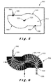
- FIG. 1 illustrates a first embodiment of a measurement device 100 in accordance with the present invention.
- the device 100 comprises a closed measurement chamber 110 that is shaped as an irregular hexagon.
- the measurement chamber 110 is constructed as a substantially two-dimensional device having at least one partly conic shape.
- the conic shape is provided by a substantially elliptical surface 120 located within the measurement chamber 110. Electromagnetic signals are directed onto a sample located within the chamber 110 using the elliptical surface 120. Similarly, electromagnetic signals reflected from the sample are directed out of the measurement chamber 110 using the substantially elliptical surface 120.
- the substantially elliptical surface 120 forms part of an ellipse 130 whose outline is indicated by a dotted line.
- the ellipse 130 is a regular ellipse having a first focal point 140 and a second focal point 150.
- the first and second focal points 140, 150 are used to position an input/output port 160 through which electromagnetic signals are applied to the sample and a holder for receiving a sample to be tested (not shown) respectively.
- the input/output port 160 includes an antenna 170 for directing the electromagnetic signals into the chamber 110 and onto the substantially elliptical surface 120 for reflection to and from the sample being tested.
- Wall 180 of the measurement chamber 110 is covered by electromagnetic absorbing material (not shown) which prevents interference between radiation reflected from the walls of the measurement chamber 110 and the reflected radiation from the sample. In this way, radiation incident on the wall 180 of the measurement chamber 110 is not reflected but absorbed so that only the reflected radiation from the sample in the sample holder (not shown) is received at the input/output port 160 via the antenna 170.
- An electromagnetic wave is applied to the input/output port 160 and to the antenna 170 from which the signals are transmitted through the chamber 110 and to the sample located at focal point 150 via the elliptical surface 120.
- Signals reflected from the sample are received by the antenna 170 via the elliptical surface 120 and passed to a processor (not shown) for processing.
- the processor determines the permittivity and permeability of the sample from the reflected electromagnetic signals.
- the processor may comprise a network analyser and a computer that is connected to the input/output port 140 via a waveguide or a coaxial cable.
- the processor may also control the generation of the electromagnetic signal that is applied to the sample via the input/output port 160, the antenna 170 and the elliptical surface 120.
- a plan view of the measurement chamber 100 is shown in Figure 1 , and in order to provide a substantially two-dimensional measurement, the thickness or depth of the chamber is of the order of the wavelength of the electromagnetic radiation used, typically a few millimetres at millimetre-wave frequencies.
- FIG. 2 a second embodiment of a measurement device 200 in accordance with the present invention is shown.
- the measurement device 200 comprises a substantially two-dimensional chamber 210 constructed with a combination of two substantially elliptical surfaces 220, 225.
- each substantially elliptical surface 220, 225 forms part of an ellipse 230, 235 as indicated by the dotted lines.
- Ellipse 230 has two focal points 240, 250 and ellipse 235 has two focal points 245, 255 with focal point 250 of ellipse 230 and focal point 255 of ellipse 235 overlapping, that is, they are coincident.
- the measurement device 200 also includes a first input/output port 260 and a second input/output port 265.
- Each input/output port 260, 265 includes an antenna 270, 275 for directing electromagnetic signals onto and from respective elliptical surfaces 220, 225 within the measurement chamber 210, the input/output ports 240, 245 and the antennas 270, 275 being positioned at the non-overlapping or non-coincident focal points 240, 245 of respective ones of the ellipses 230, 235.
- Each input/output port 260, 265 is connected to a waveguide or coaxial cable (not shown) at the outside of the measurement device 200.
- a sample holder (not shown) is positioned at the overlapping focal point 250, 255.
- the measurement chamber 210 is defined by walls 280, 285 and the elliptical surfaces 220, 225, the walls 280, 285 forming part of a housing 290 that is shaped to accommodate the elliptical surfaces 220, 225 as shown.
- the walls 280, 285 are covered with electromagnetic absorbing material (not shown) to prevent reflected radiation from these walls interfering with electromagnetic radiation reflected from and transmitted through the sample.
- an electromagnetic signal is provided to the first input/output port 260 where it is directed by the associated antenna 270 towards the elliptical surface 220 and to the sample being measured that is located at the overlapping focal point 250, 255.
- Electromagnetic signals passing through the sample are collected by elliptical surface 225 and directed to the antenna 275 associated with the second input/output port 265.
- Electromagnetic signals reflected from the sample are collected by elliptical surface 220 and directed to antenna 270 associated with the first input/output port 260.
- Each input/output port 260, 265 is connected to a processor (not shown), which may comprise a network analyser and computer, by means of a waveguide or coaxial cable (also not shown).
- the processor determines the permittivity and permeability of the sample from the electromagnetic signals reflected from the sample and transmitted through the sample.
- the electromagnetic signal may alternatively be provided to the second input/output port 265 where it is directed by the associated antenna 275 towards the elliptical surface 225 and to the sample being measured that is located at the overlapping focal point 250, 255. Electromagnetic signals passing through the sample are collected by elliptical surface 220 and directed to the antenna 270 associated with the second input/output port 260. Electromagnetic signals reflected from the sample are collected by elliptical surface 225 and directed to antenna 275 associated with the first input/output port 265.
- the electromagnetic signals may be applied simultaneously, or sequentially, to both input/output ports 260, 265 and the transmitted and reflected signals processed accordingly.
- electromagnetic signals of different frequencies may be applied to respective ones of the first and second input/output ports 260, 265.
- the sample holder containing the sample of material to be examined or measured is placed at the common focal point 250, 255. This points acts as a second energy source and radiates energy towards the antennas 270, 275.
- Scattering parameters (S-parameters) are continuously measured at at least one of the input/output ports 260, 265 depending on the particular configuration of the measurement device 200.
- the insertion loss and the return loss are measured to be less than 1 dB and 10dB respectively for the whole microwave V band, that is, between 50 and 75GHz. Insertion loss is an expression of the magnitude of the transmission coefficient
- Figure 3 illustrates an electromagnetic field distribution within the measurement device 200 shown in Figure 2 .
- the antennas 270, 275 comprise H-plane horn antennas that irradiate the two elliptical surfaces 220, 225.
- the two horn antennas are implemented in a semi-two-dimensional configuration in an x-y plane and that the radiating fields are confined in the z-direction resulting in a reduced loss due to diffraction.
- the fields radiated by the first horn antenna 270 are reflected in two steps before being received by the second horn antenna 275, the first reflection step being at the elliptical surface 220 and the second reflection step being at the elliptical surface 225.
- the phase centres of the horn antennas 270, 275 are placed on the non-common focal points of the ellipses 230, 235 ( Figure 2 ) resulting in the focussing of the waves radiated from each of the horn antennas 270, 275 at the common focal point 250, 255.
- This focussing helps the apparatus to have more sensitivity to the characteristics of the particular sample material being examined.
- electromagnetic signals are substantially confined by the elliptical surfaces 220, 225 and the walls 280, 285 of the housing 290, with some leakage through a gap 310 between the elliptical surfaces 220, 225 and around ends 320, 325 of the elliptical surfaces 220, 225 adjacent the focal points 240, 245.
- the walls 280, 285 are covered with electromagnetic absorbing material and do not provide any role in the directing of the electromagnetic radiation to and from the sample.
- a measurement device 400 has been designed as shown in Figure 4 .
- FIG 4 a perspective view of the measurement device 400 is shown.
- the measurement device 400 comprises a base portion 410 and a top portion 420 that define a measurement chamber 430.
- the base portion 410 has dimensions of 10cm x 20cm and can be made out of, for example, aluminium, brass, or silicon with a metallised interior.
- the height of the measurement chamber 430 is about 2mm to provide an almost two-dimensional arrangement at the microwave V band.
- the top portion 420 comprises a substantially planar metallic cap sized to be the same as the dimensions of the base portion 410, that is, 10cm x 20cm.
- the base portion 410 is shaped to provide a generally semicircular recess that defines the measurement chamber 430.
- First and second elliptical surfaces 440, 445 are provided as shown together with first and second input/output ports 450, 455.
- the first and second input/output ports 450, 455 are located at non-common focal points of ellipses (not shown) of which the first and second elliptical surfaces 440, 445 form a part.
- the input/output ports 450, 455 are arranged to be connected with standard waveguides, for example, WR15 waveguides 460 (only one of which is shown in Figure 4 ) that are suitable for use in the microwave V band in the frequency range of 50 to 75GHz.
- the common, overlapping or coincident focal points are not shown in this Figure.
- absorbers 470, 480 are placed at the radiation boundaries, that is, along the substantially semicircular recess that defines the measurement chamber 430 but leaving the input/output ports 450, 455 clear.
- Such absorbers may comprise carbon or a graphite-based material.
- the sample holder containing the sample of material to be examined or measured is placed at the common focal point (not shown) and the common focal point acts as a second energy source and radiates energy towards the input/output ports 450, 455.
- Figure 5 illustrates a schematic plan view of another embodiment of a measurement device 500 in accordance with the present invention.
- the measurement device 500 comprises a measurement chamber 510 substantially designed as a combination of two ellipses (not shown) having first and second focal points 520, 525, 530, 535 with second focal points 525, 535 forming an overlapping focal point as shown.
- a portion of each ellipse forms an elliptically shaped surface 540, 545 which reflects radiation onto a sample holder (not shown) placed at the overlapping focal point 525, 535.
- the measurement device 500 comprises two input/output ports 550, 555 which are arranged to be connected to a waveguide or coaxial cable (not shown) at the outside of the measurement chamber 510 and to two openended waveguides (not shown) directed towards the measurement chamber 510.
- the two input/output ports 550, 555 are placed at the locations of the non-overlapping focal points 520, 530.
- the measurement device 500 directs energy from one input/output port 550, 555 located at non-coincident focal points 520, 530 towards a sample holder containing the sample of material to be examined or measured is placed at the common focal point 525, 535.
- the common, coincident or overlapping focal point 525, 535 acts as a second energy source and radiates energy towards the input/output ports 550,555.
- a field distribution for the measurement device 500 is shown in Figure 6 .
- the field distribution shown in Figure 6 is bounded by the measurement chamber 510 although here it is easier to see the location of the overlapping focal points 525, 535 as indicated at 600
- Figure 7 illustrates a graph 700 that plots the return loss and insertion loss of the device measured from the two input/output ports with respect to frequency. Return loss is indicated by dotted profile 710 and insertion loss is indicated by solid line 720. These parameters can be used to calculate the required material parameters so that return loss at least is optimised.
Landscapes
- Physics & Mathematics (AREA)
- Electromagnetism (AREA)
- Health & Medical Sciences (AREA)
- Life Sciences & Earth Sciences (AREA)
- Chemical & Material Sciences (AREA)
- Analytical Chemistry (AREA)
- Biochemistry (AREA)
- General Health & Medical Sciences (AREA)
- General Physics & Mathematics (AREA)
- Immunology (AREA)
- Pathology (AREA)
- Investigating Or Analysing Materials By Optical Means (AREA)
Abstract
Description
- The present invention relates to the determination of electromagnetic properties of samples, and is more particularly concerned with a system and method for determining such properties of small samples.
- Extraction of electromagnetic properties of materials has been performed in many forms of testing including non-destructive testing as described in
US-A-5574379 . InUS-A-5574379 , a system of measuring the electromagnetic properties of a component is described where electromagnetic energy, for example, microwave energy, is directed towards the component being tested and the reflected energy is analysed to indicate the resistivity or magnetic susceptibility of the component. - In addition, several techniques are available for characterising materials at millimetre and sub-millimetre frequencies.
-
US-A-4507602 describes a system for measuring the properties of a sample. The sample is positioned between two sectoral horns that are placed mouth-to-mouth with the sample therebetween. An input signal in the Ku band (12.4 to 18GHz) is supplied to the sample via one horn and the transmitted and reflected signals from the sample are received at respective horns. The transmitted and reflected signals are analysed to determine the complex permittivity and permeability of the sample. - It is also known to perform permittivity measurements on printed wiring, circuit boards, thin films and other substrates in order to measure their integrity. This is described by J B Jarvis and C A Jones in "Dielectric Measurements on Printed Wiring and Circuit Boards, Thin Films and Substrates: An Overview", Mat. Res. Soc. Sympo. Proc., Vol. 381, 1995.
- Fabry-Perot resonators are also known for measuring the electromagnetic properties of samples using microwaves as described in "Fabry-Perot and Open Resonators at Microwave and Millimetre Wave Frequencies, 2-300GTHz", J. Phys. E: Sci. Instrum., Vol. 15, 1982. Properties that can be measured include dielectric constant, anisotropy, and magnetic resonance.
- The measurement of dielectric constant is also described in "Determination of the Complex Permittivity of Packaging Materials at Millimeter-Wave Frequencies" by T Zwick et al., IEEE Trans. Microw. Theory Tech., Vol. 54, no. 3, 2006. Frequencies from below 20 to 100GHz are used for performing measurements on thin sheet substrate materials.
- Corrugated horn antennas can be used with elliptical surfaces for measuring laminar samples as described by J Krupka in "Frequency Domain Complex Permittivity Measurements at Microwave Frequencies", Meas. Sci. Technol., Vol. 17, .
- In the articles described above, the methods require a three-dimensional measurement to be made of the small sample and correct alignment of the sample in three dimensions is required to have good measurement results.
- In
US-A-5455516 , a method and apparatus for the measurement of moisture in a material is described. Microwave energy is coupled to a measurement chamber via a coaxial transmission line over a multi-octave bandwidth via an intermediate microstrip-to-slotline coupling circuit. - However, most of these methods or techniques use samples with large dimensions and tend to be unsuitable for measuring the electromagnetic properties of small samples. In addition, the sample needs to be correctly positioned within a three-dimensional space so that misalignment aberrations do not have an impact on the accuracy of the measurement.
- Moreover, known methods and apparatus tend to be over-complicated for measuring small samples, particularly synthesised materials, such as carbon nanotubes and graphene, where the size of the samples is limited.
- It is therefore an object of the present invention to provide an improved and simplified apparatus and associated method for measuring the electromagnetic characteristics of small samples.
- It is a further object of the present invention to provide apparatus and method for measuring any material parameter that can be determined from measuring the electromagnetic properties of the material.
- It is another object of the present invention to provide a device and/or method where electromagnetic measurements can be made at millimetre and sub-millimetre wave frequencies for samples with dimensions typically in the range of a few millimetres by a few millimetres or smaller.
- It is also an object of the present invention to provide a device that overcomes the problem of misalignment aberrations present in conventional three-dimensional measurement methods.
- In accordance with a first aspect of the present invention, there is provided a measurement device (100; 200; 400; 500) for measuring electromagnetic characteristics of at least sub-millimetre sized samples using electromagnetic radiation, the measurement device comprising:-
- a substantially two-dimensional measurement chamber;
- at least one input/output provided in the measurement chamber for introducing electromagnetic radiation into the measurement chamber;
- a sample holder;
- at least one reflective surface provided within the measurement chamber for directing the introduced electromagnetic radiation towards the sample holder and for directing at least reflected electromagnetic radiation from the sample holder; and
- a controller for controlling the introduced electromagnetic radiation and for measuring the at least reflected electromagnetic radiation;
- characterised in that each reflective surface comprises a partly conic shape having at least two focal points;
- and in that each input/output port and the sample holder is located at one of the focal points.
- By using a partly conic shape for the reflective surface, the focal points can be used for positioning the sample holder, and hence, the sample to be tested as well as the input/output ports. This provides an efficient transfer of electromagnetic energy to and from the sample in the sample holder.
- In one embodiment, the partly conic shape comprises an ellipse and the reflective surface comprises a portion of the ellipse. Here, a single reflective surface is provided that forms the portion of an ellipse, the reflective surface having first and second focal points with one input/output port located at the first focal point and the sample holder at the second focal point.
- Preferably, the input/output port includes an antenna for directing the electromagnetic energy onto the sample holder via the reflective surface and for receiving reflected electromagnetic energy from the sample holder via the reflective surface.
- In another embodiment, two reflective surfaces are provided, each reflective surface forming the portion of an ellipse and having respective first and second focal points, and wherein the second focal point of one ellipse is coincident with the second focal point of the other ellipse, the sample holder being located at the coincident focal point with the input/output ports being located at respective ones of the first focal points.
- Each input/output port may include a respective antenna for directing the electromagnetic energy onto the sample holder via the reflective surface and for receiving reflected electromagnetic energy from the sample holder via the reflective surface.
- Preferably, at least one of the input/output ports directs electromagnetic energy into the measurement chamber. It will be appreciated that in some embodiments, both input/output ports may be required to direct energy into the measurement chamber either sequentially or simultaneously.
- In addition, at least one of the input/output ports may receive reflected electromagnetic energy from the sample holder. Similarly, at least one of the input/output ports may receive transmitted electromagnetic energy from the sample holder.
- It will be appreciated that, in one embodiment, at least one of the input/output ports may direct electromagnetic energy into the measurement chamber and/or receive reflected and/or transmitted electromagnetic energy from the sample holder.
- In some embodiments, each input/output port may comprise a waveguide.
- For a better understanding of the present invention, reference will now be made, by way of example only, to the accompanying drawings in which:-
-
Figure 1 is a schematic plan view of a measurement device in accordance with one embodiment of the present invention; -
Figure 2 is a schematic plan view of a measurement device in accordance with a second embodiment of the present invention; -
Figure 3 illustrates a radiation field distribution in the device shown inFigure 2 ; -
Figure 4 is a perspective view of the measurement device shown inFigure 2 ; -
Figure 5 is a schematic illustration of a measurement device in accordance with a third embodiment of the present invention; -
Figure 6 illustrates a radiation field distribution in the device shown inFigure 5 ; and -
Figure 7 illustrates a graph of insertion and return losses against frequency for a measurement device in accordance with the present invention. - The present invention will be described with respect to particular embodiments and with reference to certain drawings but the invention is not limited thereto. The drawings described are only schematic and are non-limiting. In the drawings, the size of some of the elements may be exaggerated and not drawn on scale for illustrative purposes.
- It will be understood that the terms "vertical" and "horizontal" are used herein refer to particular orientations of the Figures and these terms are not limitations to the specific embodiments described herein.
- The terms "first", "second", "third" and the like are used in the description for distinguishing between similar elements and not necessarily for describing a sequential or chronological order. It will be appreciated that the terms are interchangeable under appropriate circumstances and that the embodiments of the invention can operate in other sequences than described or illustrated herein if necessary.
- In accordance with the present invention, the particular characteristics to be determined in relation to a sample are electromagnetic permittivity and the magnetic permeability of the material. However, it will be appreciated that other characteristics may also be determined.
- The present invention will be described with reference to samples made from carbon nanotubes and graphene. Graphene is an allotrope of carbon whose structure is one atom thick planar sheets of bonded carbon atoms densely packed in a honeycomb crystal lattice. The crystalline or "flake" form of graphite consists of many graphene sheets stacked together.
- Carbon nanotubes (CNTs) are allotropes of carbon with a cylindrical nanostructure which have unusual properties. Their name is derived from their long hollow structure with walls formed by one atom thick sheets of carbon called graphene. The sheets of graphene are rolled at specific and discrete chiral angles to form the CNT, the combination of the rolling angle and the radius of the tube determines the properties of the CNT formed. CNTs are used in many technical areas including, but not limited to, nanotechnology, electronics and optics.
- In accordance with the present invention, a device for the measurement of electromagnetic characteristics of small samples of synthesised materials is described that uses a two-dimensional geometry. As a result, the device tends not to suffer from misalignment aberrations that occur in three-dimensional devices.
- The present invention relates to a device for investigating or examining electromagnetic properties of small samples of material. The device comprises a material measurement chamber, at least one input port for transmitting electromagnetic signals into the measurement chamber and for receiving electromagnetic signals from the measurement chamber. Each input port may include an antenna coupled thereto and through which the electromagnetic signals are channelled for both transmission and reception.
- The measurement device in accordance with the embodiments of the present invention described below uses a controllable source of electromagnetic energy having a selected frequency. The source of electromagnetic energy is coupled to a measurement chamber by means of probes, waveguides, loops, antennas, apertures or other suitable structures so as to establish an electromagnetic wave inside the measurement chamber so that the wave can interact with the sample located within the measurement chamber.
- The term "electromagnetic signal" as used herein refers to the means for generating the electromagnetic wave within the measurement chamber. The term is also used to refer to the electromagnetic waves that are received for processing.
-
Figure 1 illustrates a first embodiment of ameasurement device 100 in accordance with the present invention. Thedevice 100 comprises aclosed measurement chamber 110 that is shaped as an irregular hexagon. Themeasurement chamber 110 is constructed as a substantially two-dimensional device having at least one partly conic shape. In this embodiment, the conic shape is provided by a substantiallyelliptical surface 120 located within themeasurement chamber 110. Electromagnetic signals are directed onto a sample located within thechamber 110 using theelliptical surface 120. Similarly, electromagnetic signals reflected from the sample are directed out of themeasurement chamber 110 using the substantiallyelliptical surface 120. - The substantially
elliptical surface 120 forms part of anellipse 130 whose outline is indicated by a dotted line. Theellipse 130 is a regular ellipse having a firstfocal point 140 and a secondfocal point 150. The first and secondfocal points output port 160 through which electromagnetic signals are applied to the sample and a holder for receiving a sample to be tested (not shown) respectively. The input/output port 160 includes anantenna 170 for directing the electromagnetic signals into thechamber 110 and onto the substantiallyelliptical surface 120 for reflection to and from the sample being tested. -
Wall 180 of themeasurement chamber 110 is covered by electromagnetic absorbing material (not shown) which prevents interference between radiation reflected from the walls of themeasurement chamber 110 and the reflected radiation from the sample. In this way, radiation incident on thewall 180 of themeasurement chamber 110 is not reflected but absorbed so that only the reflected radiation from the sample in the sample holder (not shown) is received at the input/output port 160 via theantenna 170. - An electromagnetic wave is applied to the input/
output port 160 and to theantenna 170 from which the signals are transmitted through thechamber 110 and to the sample located atfocal point 150 via theelliptical surface 120. Signals reflected from the sample are received by theantenna 170 via theelliptical surface 120 and passed to a processor (not shown) for processing. The processor determines the permittivity and permeability of the sample from the reflected electromagnetic signals. - The processor may comprise a network analyser and a computer that is connected to the input/
output port 140 via a waveguide or a coaxial cable. - It will be appreciated that the processor may also control the generation of the electromagnetic signal that is applied to the sample via the input/
output port 160, theantenna 170 and theelliptical surface 120. - A plan view of the
measurement chamber 100 is shown inFigure 1 , and in order to provide a substantially two-dimensional measurement, the thickness or depth of the chamber is of the order of the wavelength of the electromagnetic radiation used, typically a few millimetres at millimetre-wave frequencies. - In
Figure 2 , a second embodiment of ameasurement device 200 in accordance with the present invention is shown. Themeasurement device 200 comprises a substantially two-dimensional chamber 210 constructed with a combination of two substantiallyelliptical surfaces elliptical surface ellipse Ellipse 230 has twofocal points ellipse 235 has twofocal points focal point 250 ofellipse 230 andfocal point 255 ofellipse 235 overlapping, that is, they are coincident. - The
measurement device 200 also includes a first input/output port 260 and a second input/output port 265. Each input/output port antenna elliptical surfaces measurement chamber 210, the input/output ports antennas focal points ellipses output port measurement device 200. In addition, a sample holder (not shown) is positioned at the overlappingfocal point - The
measurement chamber 210 is defined bywalls elliptical surfaces walls housing 290 that is shaped to accommodate theelliptical surfaces walls - During sample measurement, an electromagnetic signal is provided to the first input/
output port 260 where it is directed by the associatedantenna 270 towards theelliptical surface 220 and to the sample being measured that is located at the overlappingfocal point elliptical surface 225 and directed to theantenna 275 associated with the second input/output port 265. Electromagnetic signals reflected from the sample are collected byelliptical surface 220 and directed toantenna 270 associated with the first input/output port 260. - Each input/
output port - It will be appreciated that, during measurement, the electromagnetic signal may alternatively be provided to the second input/
output port 265 where it is directed by the associatedantenna 275 towards theelliptical surface 225 and to the sample being measured that is located at the overlappingfocal point elliptical surface 220 and directed to theantenna 270 associated with the second input/output port 260. Electromagnetic signals reflected from the sample are collected byelliptical surface 225 and directed toantenna 275 associated with the first input/output port 265. - In some instances, the electromagnetic signals may be applied simultaneously, or sequentially, to both input/
output ports output ports - The sample holder containing the sample of material to be examined or measured is placed at the common
focal point antennas output ports measurement device 200. In particular, the insertion loss and the return loss are measured to be less than 1 dB and 10dB respectively for the whole microwave V band, that is, between 50 and 75GHz. Insertion loss is an expression of the magnitude of the transmission coefficient |S21| in dB and return loss is an expression of the magnitude of the reflection coefficient |S11| in dB. -
Figure 3 illustrates an electromagnetic field distribution within themeasurement device 200 shown inFigure 2 . Components that have previously been described with reference toFigure 2 have the same reference numerals. InFigure 3 , theantennas elliptical surfaces first horn antenna 270 are reflected in two steps before being received by thesecond horn antenna 275, the first reflection step being at theelliptical surface 220 and the second reflection step being at theelliptical surface 225. - The phase centres of the
horn antennas ellipses 230, 235 (Figure 2 ) resulting in the focussing of the waves radiated from each of thehorn antennas focal point - It can be seen that electromagnetic signals are substantially confined by the
elliptical surfaces walls housing 290, with some leakage through agap 310 between theelliptical surfaces elliptical surfaces focal points walls - Based on the schematic design shown in
Figures 2 and3 and full wave analysis based on a finite element technique, ameasurement device 400 has been designed as shown inFigure 4 . InFigure 4 , a perspective view of themeasurement device 400 is shown. Themeasurement device 400 comprises abase portion 410 and atop portion 420 that define ameasurement chamber 430. Thebase portion 410 has dimensions of 10cm x 20cm and can be made out of, for example, aluminium, brass, or silicon with a metallised interior. The height of themeasurement chamber 430 is about 2mm to provide an almost two-dimensional arrangement at the microwave V band. Thetop portion 420 comprises a substantially planar metallic cap sized to be the same as the dimensions of thebase portion 410, that is, 10cm x 20cm. - The
base portion 410 is shaped to provide a generally semicircular recess that defines themeasurement chamber 430. First and secondelliptical surfaces output ports output ports elliptical surfaces output ports Figure 4 ) that are suitable for use in the microwave V band in the frequency range of 50 to 75GHz. The common, overlapping or coincident focal points are not shown in this Figure. - In addition, in order to avoid unwanted resonances from the edges and interfering diffractions,
absorbers measurement chamber 430 but leaving the input/output ports - The sample holder containing the sample of material to be examined or measured is placed at the common focal point (not shown) and the common focal point acts as a second energy source and radiates energy towards the input/
output ports -
Figure 5 illustrates a schematic plan view of another embodiment of ameasurement device 500 in accordance with the present invention. As before, themeasurement device 500 comprises ameasurement chamber 510 substantially designed as a combination of two ellipses (not shown) having first and secondfocal points focal points surface focal point measurement device 500 comprises two input/output ports measurement chamber 510 and to two openended waveguides (not shown) directed towards themeasurement chamber 510. The two input/output ports focal points - In a similar way to the
measurement devices 200, 400 (Figures 2 &4 respectively), themeasurement device 500 directs energy from one input/output port focal points focal point focal point - A field distribution for the
measurement device 500 is shown inFigure 6 . In a similar way to field distribution shown inFigure 3 , the field distribution shown inFigure 6 is bounded by themeasurement chamber 510 although here it is easier to see the location of the overlappingfocal points -
Figure 7 illustrates agraph 700 that plots the return loss and insertion loss of the device measured from the two input/output ports with respect to frequency. Return loss is indicated bydotted profile 710 and insertion loss is indicated bysolid line 720. These parameters can be used to calculate the required material parameters so that return loss at least is optimised. - Although the present invention has been described with reference to specific embodiments, it will be appreciated that other configurations of measurement devices are possible provided there is an overlapping focal point which can be determined from the surface geometry of the elliptical surfaces.
Claims (11)
- A measurement device (100; 200; 400; 500) for measuring electromagnetic characteristics of at least sub-millimetre sized samples using electromagnetic radiation, the measurement device comprising:-
a substantially two-dimensional measurement chamber (110; 210; 430; 510);
at least one input/output port (160, 170; 260, 265, 270, 275; 550, 555) provided in the measurement chamber (110; 210; 430; 510) for introducing electromagnetic radiation into the measurement chamber (110; 210; 430; 510);
a sample holder;
at least one reflective surface (120; 220, 225; 440, 445; 540, 545) provided within the measurement chamber (110; 210; 430; 510) for directing the introduced electromagnetic radiation towards the sample holder and for directing at least reflected electromagnetic radiation from the sample holder; and
a controller for controlling the introduced electromagnetic radiation and for measuring the at least reflected electromagnetic radiation;
characterised in that each reflective surface (120; 220, 225; 440, 445; 540, 545) comprises a partly conic shape (130; 230, 235; 540, 545) having at least two focal points (140, 150; 240, 245, 250, 255; 450, 455; 520, 525, 530, 535);
and in that each input/output port (160, 170; 260, 265, 270, 275; 550, 555) and the sample holder is located at one of the focal points (140, 150; 240, 245, 250, 255; 450, 455; 520, 525, 530, 535). - A measurement device according to claim 1, wherein the partly conic shape comprises an ellipse (130; 230, 235) and the reflective surface (120; 220, 225; 440, 445; 540, 545) comprises a portion of the ellipse (130; 230, 235).
- A measurement device according to claim 2, wherein a single reflective surface (120) is provided that forms the portion of an ellipse (130), the reflective surface (120) having first and second focal points (140, 150) with one input/output port (160, 170) located at the first focal point (140) and the sample holder at the second focal point (150).
- A measurement device according to claim 3, wherein the input/output port (160, 170) includes an antenna (170) for directing the electromagnetic energy onto the sample holder via the reflective surface (120) and for receiving reflected electromagnetic energy from the sample holder via the reflective surface (120).
- A measurement device according to claim 2, wherein two reflective surfaces (220, 225; 440, 445; 540, 545) are provided, each reflective surface (220, 225; 440, 445; 540, 545) forming the portion of an ellipse (230, 235) and having respective first and second focal points (240, 245, 250, 255; 450, 455; 520, 525, 530, 535), and wherein the second focal point (250; 530) of one ellipse (230) is coincident with the second focal point (255; 535) of the other ellipse (235), the sample holder being located at the coincident focal point (250, 255; 530, 535) with the input/output ports (260, 265; 550, 555) being located at respective ones of the first focal points (240, 245; 520, 525).
- A measurement device according to claim 5, wherein each input/output port (260, 265) includes a respective antenna (270, 275) for directing the electromagnetic energy onto the sample holder via the reflective surface (220, 225) and for receiving reflected electromagnetic energy from the sample holder via the reflective surface (220, 225).
- A measurement device according to claim 5 or 6, wherein at least one of the input/output ports (260, 265, 270, 275) directs electromagnetic energy into the measurement chamber (210; 430, 510).
- A measurement device according to claim 7, wherein at least one of the input/output ports (260, 265, 270, 275) receives reflected electromagnetic energy from the sample holder.
- A measurement device according to claim 7 or 8, wherein at least one of the input/output ports (260, 265, 270, 275) receives transmitted electromagnetic energy from the sample holder.
- A measurement device according to any one of the preceding claims, wherein each input/output port (550, 555) comprises a waveguide (460).
- A measurement device according to any one of the preceding claims, wherein walls (180; 280, 285; 480) of the measurement chamber (110; 210; 410) are covered with electromagnetic absorbing material to prevent reflected electromagnetic radiation from these walls (180; 280, 285; 480) interfering with electromagnetic radiation reflected and/or transmitted from the sample.
Applications Claiming Priority (1)
| Application Number | Priority Date | Filing Date | Title |
|---|---|---|---|
| US39272510P | 2010-10-13 | 2010-10-13 |
Publications (2)
| Publication Number | Publication Date |
|---|---|
| EP2442096A1 true EP2442096A1 (en) | 2012-04-18 |
| EP2442096B1 EP2442096B1 (en) | 2013-05-22 |
Family
ID=44936173
Family Applications (1)
| Application Number | Title | Priority Date | Filing Date |
|---|---|---|---|
| EP11184867.7A Not-in-force EP2442096B1 (en) | 2010-10-13 | 2011-10-12 | Determination of electromagnetic properties of samples |
Country Status (2)
| Country | Link |
|---|---|
| US (1) | US20120092674A1 (en) |
| EP (1) | EP2442096B1 (en) |
Families Citing this family (3)
| Publication number | Priority date | Publication date | Assignee | Title |
|---|---|---|---|---|
| US20140327586A1 (en) * | 2013-05-03 | 2014-11-06 | The Howland Company | Reflective Ellipsoid Chamber |
| DE102019121995A1 (en) | 2019-08-15 | 2021-02-18 | Endress+Hauser SE+Co. KG | Measuring device for determining a dielectric value |
| FR3161279A1 (en) * | 2024-04-16 | 2025-10-17 | Terradona | System for characterizing a material or matter of an object or moving body and associated installation for collecting or sorting objects |
Citations (4)
| Publication number | Priority date | Publication date | Assignee | Title |
|---|---|---|---|---|
| US4507602A (en) | 1982-08-13 | 1985-03-26 | The United States Of America As Represented By The Secretary Of The Air Force | Measurement of permittivity and permeability of microwave materials |
| US5455516A (en) | 1992-04-21 | 1995-10-03 | Thermedics Inc. | Meter and method for in situ measurement of the electromagnetic properties of various process materials using cutoff frequency characterization and analysis |
| US5574379A (en) | 1992-12-17 | 1996-11-12 | Northrop Grumman Corporation | System for measuring electromagnetic properties |
| US20040095147A1 (en) * | 2001-01-30 | 2004-05-20 | Cole Bryan Edward | Probe apparatus and method for examining a sample |
Family Cites Families (13)
| Publication number | Priority date | Publication date | Assignee | Title |
|---|---|---|---|---|
| US4189236A (en) * | 1978-03-20 | 1980-02-19 | Coulter Electronics, Inc. | Ellipsoid-conic radiation collector and method |
| US4523841A (en) * | 1979-03-15 | 1985-06-18 | Coulter Electronics, Inc. | Radiant energy reradiating flow cell system and method |
| US4716293A (en) * | 1986-05-16 | 1987-12-29 | Harrick Nicolas J | Accessory for infrared emission spectroscopy |
| US4858090A (en) * | 1987-06-26 | 1989-08-15 | Downs James W | Ellipsoidal reflector concentration of energy system |
| CA2019941C (en) * | 1989-07-13 | 1994-01-25 | Toshio Abe | Electrostatic levitation furnace |
| DK108691D0 (en) * | 1991-06-07 | 1991-06-07 | Allan Goettsche | MEASUREMENT OF INDUCED DOUBLE BREAKING |
| US5467189A (en) * | 1993-01-22 | 1995-11-14 | Venturedyne, Ltd. | Improved particle sensor and method for assaying a particle |
| US5767967A (en) * | 1997-01-02 | 1998-06-16 | Yufa; Aleksandr L. | Method and device for precise counting and measuring the particulates and small bodies |
| US6034769A (en) * | 1997-06-27 | 2000-03-07 | Yufa; Aleksandr L. | Method and device for counting and measuring particles |
| US6594009B2 (en) * | 2001-02-27 | 2003-07-15 | Honeywell International Inc. | Flow cytometer and ultraviolet light disinfecting systems |
| US20110178409A1 (en) * | 2004-02-27 | 2011-07-21 | Optiscan Pty Ltd | Optical Element |
| US7671985B1 (en) * | 2006-03-13 | 2010-03-02 | Milan Milosevic | Device for small spot analysis using fiber optic interfaced spectrometers |
| US8969838B2 (en) * | 2009-04-09 | 2015-03-03 | Asml Netherlands B.V. | Systems and methods for protecting an EUV light source chamber from high pressure source material leaks |
-
2011
- 2011-10-12 EP EP11184867.7A patent/EP2442096B1/en not_active Not-in-force
- 2011-10-13 US US13/272,818 patent/US20120092674A1/en not_active Abandoned
Patent Citations (4)
| Publication number | Priority date | Publication date | Assignee | Title |
|---|---|---|---|---|
| US4507602A (en) | 1982-08-13 | 1985-03-26 | The United States Of America As Represented By The Secretary Of The Air Force | Measurement of permittivity and permeability of microwave materials |
| US5455516A (en) | 1992-04-21 | 1995-10-03 | Thermedics Inc. | Meter and method for in situ measurement of the electromagnetic properties of various process materials using cutoff frequency characterization and analysis |
| US5574379A (en) | 1992-12-17 | 1996-11-12 | Northrop Grumman Corporation | System for measuring electromagnetic properties |
| US20040095147A1 (en) * | 2001-01-30 | 2004-05-20 | Cole Bryan Edward | Probe apparatus and method for examining a sample |
Non-Patent Citations (4)
| Title |
|---|
| "Fabry-Perot and Open Resonators at Microwave and Millimetre Wave Frequencies, 2-300GTHz", J. PHYS. E: SCI. INSTRUM., vol. 15, 1982 |
| J B JARVIS, C A JONES: "Dielectric Measurements on Printed Wiring and Circuit Boards, Thin Films and Substrates: An Overview", MAT. RES. SOC. SYMPO. PROC., vol. 381, 1995 |
| J KRUPKA: "Frequency Domain Complex Permittivity Measurements at Microwave Frequencies", MEAS. SCI. TECHNOL., vol. 17, 2006, XP020103570, DOI: doi:10.1088/0957-0233/17/6/R01 |
| T ZWICK ET AL.: "Determination of the Complex Permittivity of Packaging Materials at Millimeter-Wave Frequencies", IEEE TRANS. MICROW. THEORY TECH., vol. 54, no. 3, 2006, XP001524234, DOI: doi:10.1109/TMTT.2005.864140 |
Also Published As
| Publication number | Publication date |
|---|---|
| EP2442096B1 (en) | 2013-05-22 |
| US20120092674A1 (en) | 2012-04-19 |
Similar Documents
| Publication | Publication Date | Title |
|---|---|---|
| CN102576044B (en) | The characteristic of the antenna in waveguide is determined | |
| CN209606521U (en) | A kind of hexagon complementary openings resonant ring micro belt sensor of Measuring Dielectric Constant | |
| CN113049883B (en) | Single fiber dielectric constant testing device based on coupling microstrip line | |
| Hyde IV et al. | Nondestructive determination of the permittivity tensor of a uniaxial material using a two-port clamped coaxial probe | |
| RU2665593C1 (en) | Material dielectric properties measuring method and device for its implementation | |
| US7130755B2 (en) | Near-field scanning microwave microscope using dielectric resonator | |
| Hyde et al. | A broadband, nondestructive microwave sensor for characterizing magnetic sheet materials | |
| EP2442096B1 (en) | Determination of electromagnetic properties of samples | |
| Dvorsky et al. | Microwave surface conductivity measurement using an open-ended circular waveguide probe | |
| JP3510256B2 (en) | Apparatus for non-destructive testing of dielectric / magnetic materials | |
| US8461851B2 (en) | Systems for transverse electromagnetic mode in-situ soil testing | |
| Moll | Damage detection and localization in metallic structures based on jointed electromagnetic waveguides: a proof-of-principle study | |
| US6859047B2 (en) | Anechoic test chamber and method of determining a loss characteristic of a material specimen | |
| Gu et al. | Measurement accuracy and repeatability in near-field scanning microwave microscopy | |
| Dvorsky et al. | Crack sizing using dual-polarized microwave SAR imaging | |
| Requena et al. | Wireless complex permittivity measurement using resonant scatterers and a radar approach | |
| Dester et al. | Two-iris method for the electromagnetic characterization of conductor-backed absorbing materials using an open-ended waveguide probe | |
| Wang et al. | Compact near-field microwave microscope based on the multi-port technique | |
| Idei et al. | Adaptive array technique for differential-phase reflectometry in QUEST | |
| Amiet et al. | Free space microwave permittivity and permeability measurements | |
| Gu et al. | Reflection Method for Shielding Effectiveness Measurement: Complex Materials Without Prior Knowledge | |
| Haddadi et al. | Electromagnetic wave to material interaction and microwave materials measurements | |
| Olk et al. | A Reliable Attenuation Characterization of EMI Absorber Material at V-band Frequencies | |
| Lim et al. | Simple and improved dielectric parameter extraction of thin organic packaging materials using open-ended coaxial line technique | |
| Kang | Free-Space Material Measurement for a Small Dielectric Plate at W-band |
Legal Events
| Date | Code | Title | Description |
|---|---|---|---|
| PUAI | Public reference made under article 153(3) epc to a published international application that has entered the european phase |
Free format text: ORIGINAL CODE: 0009012 |
|
| AK | Designated contracting states |
Kind code of ref document: A1 Designated state(s): AL AT BE BG CH CY CZ DE DK EE ES FI FR GB GR HR HU IE IS IT LI LT LU LV MC MK MT NL NO PL PT RO RS SE SI SK SM TR |
|
| AX | Request for extension of the european patent |
Extension state: BA ME |
|
| 17P | Request for examination filed |
Effective date: 20121018 |
|
| GRAJ | Information related to disapproval of communication of intention to grant by the applicant or resumption of examination proceedings by the epo deleted |
Free format text: ORIGINAL CODE: EPIDOSDIGR1 |
|
| GRAP | Despatch of communication of intention to grant a patent |
Free format text: ORIGINAL CODE: EPIDOSNIGR1 |
|
| GRAS | Grant fee paid |
Free format text: ORIGINAL CODE: EPIDOSNIGR3 |
|
| GRAA | (expected) grant |
Free format text: ORIGINAL CODE: 0009210 |
|
| RAP1 | Party data changed (applicant data changed or rights of an application transferred) |
Owner name: IMEC Owner name: KATHOLIEKE UNIVERSITEIT LEUVEN, K.U. LEUVEN R&D |
|
| AK | Designated contracting states |
Kind code of ref document: B1 Designated state(s): AL AT BE BG CH CY CZ DE DK EE ES FI FR GB GR HR HU IE IS IT LI LT LU LV MC MK MT NL NO PL PT RO RS SE SI SK SM TR |
|
| REG | Reference to a national code |
Ref country code: GB Ref legal event code: FG4D |
|
| REG | Reference to a national code |
Ref country code: CH Ref legal event code: EP |
|
| REG | Reference to a national code |
Ref country code: AT Ref legal event code: REF Ref document number: 613473 Country of ref document: AT Kind code of ref document: T Effective date: 20130615 |
|
| REG | Reference to a national code |
Ref country code: IE Ref legal event code: FG4D |
|
| REG | Reference to a national code |
Ref country code: DE Ref legal event code: R096 Ref document number: 602011001731 Country of ref document: DE Effective date: 20130725 |
|
| REG | Reference to a national code |
Ref country code: AT Ref legal event code: MK05 Ref document number: 613473 Country of ref document: AT Kind code of ref document: T Effective date: 20130522 |
|
| REG | Reference to a national code |
Ref country code: LT Ref legal event code: MG4D |
|
| PG25 | Lapsed in a contracting state [announced via postgrant information from national office to epo] |
Ref country code: ES Free format text: LAPSE BECAUSE OF FAILURE TO SUBMIT A TRANSLATION OF THE DESCRIPTION OR TO PAY THE FEE WITHIN THE PRESCRIBED TIME-LIMIT Effective date: 20130902 Ref country code: NO Free format text: LAPSE BECAUSE OF FAILURE TO SUBMIT A TRANSLATION OF THE DESCRIPTION OR TO PAY THE FEE WITHIN THE PRESCRIBED TIME-LIMIT Effective date: 20130822 Ref country code: AT Free format text: LAPSE BECAUSE OF FAILURE TO SUBMIT A TRANSLATION OF THE DESCRIPTION OR TO PAY THE FEE WITHIN THE PRESCRIBED TIME-LIMIT Effective date: 20130522 Ref country code: LT Free format text: LAPSE BECAUSE OF FAILURE TO SUBMIT A TRANSLATION OF THE DESCRIPTION OR TO PAY THE FEE WITHIN THE PRESCRIBED TIME-LIMIT Effective date: 20130522 Ref country code: SI Free format text: LAPSE BECAUSE OF FAILURE TO SUBMIT A TRANSLATION OF THE DESCRIPTION OR TO PAY THE FEE WITHIN THE PRESCRIBED TIME-LIMIT Effective date: 20130522 Ref country code: SE Free format text: LAPSE BECAUSE OF FAILURE TO SUBMIT A TRANSLATION OF THE DESCRIPTION OR TO PAY THE FEE WITHIN THE PRESCRIBED TIME-LIMIT Effective date: 20130522 Ref country code: FI Free format text: LAPSE BECAUSE OF FAILURE TO SUBMIT A TRANSLATION OF THE DESCRIPTION OR TO PAY THE FEE WITHIN THE PRESCRIBED TIME-LIMIT Effective date: 20130522 Ref country code: PT Free format text: LAPSE BECAUSE OF FAILURE TO SUBMIT A TRANSLATION OF THE DESCRIPTION OR TO PAY THE FEE WITHIN THE PRESCRIBED TIME-LIMIT Effective date: 20130923 Ref country code: GR Free format text: LAPSE BECAUSE OF FAILURE TO SUBMIT A TRANSLATION OF THE DESCRIPTION OR TO PAY THE FEE WITHIN THE PRESCRIBED TIME-LIMIT Effective date: 20130823 |
|
| REG | Reference to a national code |
Ref country code: NL Ref legal event code: VDEP Effective date: 20130522 |
|
| PG25 | Lapsed in a contracting state [announced via postgrant information from national office to epo] |
Ref country code: PL Free format text: LAPSE BECAUSE OF FAILURE TO SUBMIT A TRANSLATION OF THE DESCRIPTION OR TO PAY THE FEE WITHIN THE PRESCRIBED TIME-LIMIT Effective date: 20130522 Ref country code: RS Free format text: LAPSE BECAUSE OF FAILURE TO SUBMIT A TRANSLATION OF THE DESCRIPTION OR TO PAY THE FEE WITHIN THE PRESCRIBED TIME-LIMIT Effective date: 20130522 Ref country code: BG Free format text: LAPSE BECAUSE OF FAILURE TO SUBMIT A TRANSLATION OF THE DESCRIPTION OR TO PAY THE FEE WITHIN THE PRESCRIBED TIME-LIMIT Effective date: 20130822 Ref country code: HR Free format text: LAPSE BECAUSE OF FAILURE TO SUBMIT A TRANSLATION OF THE DESCRIPTION OR TO PAY THE FEE WITHIN THE PRESCRIBED TIME-LIMIT Effective date: 20130522 |
|
| PG25 | Lapsed in a contracting state [announced via postgrant information from national office to epo] |
Ref country code: LV Free format text: LAPSE BECAUSE OF FAILURE TO SUBMIT A TRANSLATION OF THE DESCRIPTION OR TO PAY THE FEE WITHIN THE PRESCRIBED TIME-LIMIT Effective date: 20130522 |
|
| PG25 | Lapsed in a contracting state [announced via postgrant information from national office to epo] |
Ref country code: SK Free format text: LAPSE BECAUSE OF FAILURE TO SUBMIT A TRANSLATION OF THE DESCRIPTION OR TO PAY THE FEE WITHIN THE PRESCRIBED TIME-LIMIT Effective date: 20130522 Ref country code: DK Free format text: LAPSE BECAUSE OF FAILURE TO SUBMIT A TRANSLATION OF THE DESCRIPTION OR TO PAY THE FEE WITHIN THE PRESCRIBED TIME-LIMIT Effective date: 20130522 Ref country code: EE Free format text: LAPSE BECAUSE OF FAILURE TO SUBMIT A TRANSLATION OF THE DESCRIPTION OR TO PAY THE FEE WITHIN THE PRESCRIBED TIME-LIMIT Effective date: 20130522 Ref country code: BE Free format text: LAPSE BECAUSE OF FAILURE TO SUBMIT A TRANSLATION OF THE DESCRIPTION OR TO PAY THE FEE WITHIN THE PRESCRIBED TIME-LIMIT Effective date: 20130522 Ref country code: CZ Free format text: LAPSE BECAUSE OF FAILURE TO SUBMIT A TRANSLATION OF THE DESCRIPTION OR TO PAY THE FEE WITHIN THE PRESCRIBED TIME-LIMIT Effective date: 20130522 |
|
| PG25 | Lapsed in a contracting state [announced via postgrant information from national office to epo] |
Ref country code: RO Free format text: LAPSE BECAUSE OF FAILURE TO SUBMIT A TRANSLATION OF THE DESCRIPTION OR TO PAY THE FEE WITHIN THE PRESCRIBED TIME-LIMIT Effective date: 20130522 Ref country code: IT Free format text: LAPSE BECAUSE OF FAILURE TO SUBMIT A TRANSLATION OF THE DESCRIPTION OR TO PAY THE FEE WITHIN THE PRESCRIBED TIME-LIMIT Effective date: 20130522 Ref country code: NL Free format text: LAPSE BECAUSE OF FAILURE TO SUBMIT A TRANSLATION OF THE DESCRIPTION OR TO PAY THE FEE WITHIN THE PRESCRIBED TIME-LIMIT Effective date: 20130522 |
|
| PLBE | No opposition filed within time limit |
Free format text: ORIGINAL CODE: 0009261 |
|
| STAA | Information on the status of an ep patent application or granted ep patent |
Free format text: STATUS: NO OPPOSITION FILED WITHIN TIME LIMIT |
|
| 26N | No opposition filed |
Effective date: 20140225 |
|
| PG25 | Lapsed in a contracting state [announced via postgrant information from national office to epo] |
Ref country code: MC Free format text: LAPSE BECAUSE OF FAILURE TO SUBMIT A TRANSLATION OF THE DESCRIPTION OR TO PAY THE FEE WITHIN THE PRESCRIBED TIME-LIMIT Effective date: 20130522 |
|
| REG | Reference to a national code |
Ref country code: DE Ref legal event code: R097 Ref document number: 602011001731 Country of ref document: DE Effective date: 20140225 |
|
| REG | Reference to a national code |
Ref country code: IE Ref legal event code: MM4A |
|
| PG25 | Lapsed in a contracting state [announced via postgrant information from national office to epo] |
Ref country code: IE Free format text: LAPSE BECAUSE OF NON-PAYMENT OF DUE FEES Effective date: 20131012 |
|
| PG25 | Lapsed in a contracting state [announced via postgrant information from national office to epo] |
Ref country code: SM Free format text: LAPSE BECAUSE OF FAILURE TO SUBMIT A TRANSLATION OF THE DESCRIPTION OR TO PAY THE FEE WITHIN THE PRESCRIBED TIME-LIMIT Effective date: 20130522 |
|
| REG | Reference to a national code |
Ref country code: CH Ref legal event code: PL |
|
| PG25 | Lapsed in a contracting state [announced via postgrant information from national office to epo] |
Ref country code: TR Free format text: LAPSE BECAUSE OF FAILURE TO SUBMIT A TRANSLATION OF THE DESCRIPTION OR TO PAY THE FEE WITHIN THE PRESCRIBED TIME-LIMIT Effective date: 20130522 Ref country code: CY Free format text: LAPSE BECAUSE OF FAILURE TO SUBMIT A TRANSLATION OF THE DESCRIPTION OR TO PAY THE FEE WITHIN THE PRESCRIBED TIME-LIMIT Effective date: 20130522 |
|
| PG25 | Lapsed in a contracting state [announced via postgrant information from national office to epo] |
Ref country code: HU Free format text: LAPSE BECAUSE OF FAILURE TO SUBMIT A TRANSLATION OF THE DESCRIPTION OR TO PAY THE FEE WITHIN THE PRESCRIBED TIME-LIMIT; INVALID AB INITIO Effective date: 20111012 Ref country code: LI Free format text: LAPSE BECAUSE OF NON-PAYMENT OF DUE FEES Effective date: 20141031 Ref country code: MK Free format text: LAPSE BECAUSE OF FAILURE TO SUBMIT A TRANSLATION OF THE DESCRIPTION OR TO PAY THE FEE WITHIN THE PRESCRIBED TIME-LIMIT Effective date: 20130522 Ref country code: LU Free format text: LAPSE BECAUSE OF NON-PAYMENT OF DUE FEES Effective date: 20131012 Ref country code: CH Free format text: LAPSE BECAUSE OF NON-PAYMENT OF DUE FEES Effective date: 20141031 |
|
| PG25 | Lapsed in a contracting state [announced via postgrant information from national office to epo] |
Ref country code: MT Free format text: LAPSE BECAUSE OF FAILURE TO SUBMIT A TRANSLATION OF THE DESCRIPTION OR TO PAY THE FEE WITHIN THE PRESCRIBED TIME-LIMIT Effective date: 20130522 |
|
| PG25 | Lapsed in a contracting state [announced via postgrant information from national office to epo] |
Ref country code: IS Free format text: LAPSE BECAUSE OF FAILURE TO SUBMIT A TRANSLATION OF THE DESCRIPTION OR TO PAY THE FEE WITHIN THE PRESCRIBED TIME-LIMIT Effective date: 20130522 |
|
| REG | Reference to a national code |
Ref country code: FR Ref legal event code: PLFP Year of fee payment: 6 |
|
| REG | Reference to a national code |
Ref country code: FR Ref legal event code: PLFP Year of fee payment: 7 |
|
| REG | Reference to a national code |
Ref country code: FR Ref legal event code: PLFP Year of fee payment: 8 |
|
| PG25 | Lapsed in a contracting state [announced via postgrant information from national office to epo] |
Ref country code: AL Free format text: LAPSE BECAUSE OF FAILURE TO SUBMIT A TRANSLATION OF THE DESCRIPTION OR TO PAY THE FEE WITHIN THE PRESCRIBED TIME-LIMIT Effective date: 20130522 |
|
| PGFP | Annual fee paid to national office [announced via postgrant information from national office to epo] |
Ref country code: FR Payment date: 20190919 Year of fee payment: 9 |
|
| PGFP | Annual fee paid to national office [announced via postgrant information from national office to epo] |
Ref country code: GB Payment date: 20190923 Year of fee payment: 9 |
|
| PGFP | Annual fee paid to national office [announced via postgrant information from national office to epo] |
Ref country code: DE Payment date: 20190918 Year of fee payment: 9 |
|
| REG | Reference to a national code |
Ref country code: DE Ref legal event code: R119 Ref document number: 602011001731 Country of ref document: DE |
|
| GBPC | Gb: european patent ceased through non-payment of renewal fee |
Effective date: 20201012 |
|
| PG25 | Lapsed in a contracting state [announced via postgrant information from national office to epo] |
Ref country code: DE Free format text: LAPSE BECAUSE OF NON-PAYMENT OF DUE FEES Effective date: 20210501 Ref country code: FR Free format text: LAPSE BECAUSE OF NON-PAYMENT OF DUE FEES Effective date: 20201031 |
|
| PG25 | Lapsed in a contracting state [announced via postgrant information from national office to epo] |
Ref country code: GB Free format text: LAPSE BECAUSE OF NON-PAYMENT OF DUE FEES Effective date: 20201012 |