EP2439822A1 - A monolithic integrated structure comprising a buried heterostructure semiconductor optical amplifier and a photodetector - Google Patents
A monolithic integrated structure comprising a buried heterostructure semiconductor optical amplifier and a photodetector Download PDFInfo
- Publication number
- EP2439822A1 EP2439822A1 EP10306064A EP10306064A EP2439822A1 EP 2439822 A1 EP2439822 A1 EP 2439822A1 EP 10306064 A EP10306064 A EP 10306064A EP 10306064 A EP10306064 A EP 10306064A EP 2439822 A1 EP2439822 A1 EP 2439822A1
- Authority
- EP
- European Patent Office
- Prior art keywords
- waveguide
- optical
- soa
- passive
- photodetector
- Prior art date
- Legal status (The legal status is an assumption and is not a legal conclusion. Google has not performed a legal analysis and makes no representation as to the accuracy of the status listed.)
- Withdrawn
Links
Images



Classifications
-
- G—PHYSICS
- G02—OPTICS
- G02B—OPTICAL ELEMENTS, SYSTEMS OR APPARATUS
- G02B6/00—Light guides; Structural details of arrangements comprising light guides and other optical elements, e.g. couplings
- G02B6/10—Light guides; Structural details of arrangements comprising light guides and other optical elements, e.g. couplings of the optical waveguide type
- G02B6/12—Light guides; Structural details of arrangements comprising light guides and other optical elements, e.g. couplings of the optical waveguide type of the integrated circuit kind
- G02B6/12002—Three-dimensional structures
-
- H—ELECTRICITY
- H01—ELECTRIC ELEMENTS
- H01S—DEVICES USING THE PROCESS OF LIGHT AMPLIFICATION BY STIMULATED EMISSION OF RADIATION [LASER] TO AMPLIFY OR GENERATE LIGHT; DEVICES USING STIMULATED EMISSION OF ELECTROMAGNETIC RADIATION IN WAVE RANGES OTHER THAN OPTICAL
- H01S5/00—Semiconductor lasers
- H01S5/02—Structural details or components not essential to laser action
- H01S5/026—Monolithically integrated components, e.g. waveguides, monitoring photo-detectors, drivers
-
- G—PHYSICS
- G02—OPTICS
- G02B—OPTICAL ELEMENTS, SYSTEMS OR APPARATUS
- G02B6/00—Light guides; Structural details of arrangements comprising light guides and other optical elements, e.g. couplings
- G02B6/24—Coupling light guides
- G02B6/26—Optical coupling means
-
- G—PHYSICS
- G02—OPTICS
- G02B—OPTICAL ELEMENTS, SYSTEMS OR APPARATUS
- G02B6/00—Light guides; Structural details of arrangements comprising light guides and other optical elements, e.g. couplings
- G02B6/10—Light guides; Structural details of arrangements comprising light guides and other optical elements, e.g. couplings of the optical waveguide type
- G02B6/12—Light guides; Structural details of arrangements comprising light guides and other optical elements, e.g. couplings of the optical waveguide type of the integrated circuit kind
-
- G—PHYSICS
- G02—OPTICS
- G02B—OPTICAL ELEMENTS, SYSTEMS OR APPARATUS
- G02B6/00—Light guides; Structural details of arrangements comprising light guides and other optical elements, e.g. couplings
- G02B6/10—Light guides; Structural details of arrangements comprising light guides and other optical elements, e.g. couplings of the optical waveguide type
- G02B6/12—Light guides; Structural details of arrangements comprising light guides and other optical elements, e.g. couplings of the optical waveguide type of the integrated circuit kind
- G02B6/12004—Combinations of two or more optical elements
-
- H—ELECTRICITY
- H01—ELECTRIC ELEMENTS
- H01S—DEVICES USING THE PROCESS OF LIGHT AMPLIFICATION BY STIMULATED EMISSION OF RADIATION [LASER] TO AMPLIFY OR GENERATE LIGHT; DEVICES USING STIMULATED EMISSION OF ELECTROMAGNETIC RADIATION IN WAVE RANGES OTHER THAN OPTICAL
- H01S5/00—Semiconductor lasers
- H01S5/02—Structural details or components not essential to laser action
- H01S5/026—Monolithically integrated components, e.g. waveguides, monitoring photo-detectors, drivers
- H01S5/0262—Photo-diodes, e.g. transceiver devices, bidirectional devices
-
- H—ELECTRICITY
- H01—ELECTRIC ELEMENTS
- H01S—DEVICES USING THE PROCESS OF LIGHT AMPLIFICATION BY STIMULATED EMISSION OF RADIATION [LASER] TO AMPLIFY OR GENERATE LIGHT; DEVICES USING STIMULATED EMISSION OF ELECTROMAGNETIC RADIATION IN WAVE RANGES OTHER THAN OPTICAL
- H01S5/00—Semiconductor lasers
- H01S5/50—Amplifier structures not provided for in groups H01S5/02 - H01S5/30
-
- G—PHYSICS
- G02—OPTICS
- G02B—OPTICAL ELEMENTS, SYSTEMS OR APPARATUS
- G02B6/00—Light guides; Structural details of arrangements comprising light guides and other optical elements, e.g. couplings
- G02B6/10—Light guides; Structural details of arrangements comprising light guides and other optical elements, e.g. couplings of the optical waveguide type
- G02B6/12—Light guides; Structural details of arrangements comprising light guides and other optical elements, e.g. couplings of the optical waveguide type of the integrated circuit kind
- G02B2006/12083—Constructional arrangements
- G02B2006/12121—Laser
-
- G—PHYSICS
- G02—OPTICS
- G02B—OPTICAL ELEMENTS, SYSTEMS OR APPARATUS
- G02B6/00—Light guides; Structural details of arrangements comprising light guides and other optical elements, e.g. couplings
- G02B6/10—Light guides; Structural details of arrangements comprising light guides and other optical elements, e.g. couplings of the optical waveguide type
- G02B6/12—Light guides; Structural details of arrangements comprising light guides and other optical elements, e.g. couplings of the optical waveguide type of the integrated circuit kind
- G02B2006/12133—Functions
- G02B2006/12147—Coupler
-
- G—PHYSICS
- G02—OPTICS
- G02B—OPTICAL ELEMENTS, SYSTEMS OR APPARATUS
- G02B6/00—Light guides; Structural details of arrangements comprising light guides and other optical elements, e.g. couplings
- G02B6/10—Light guides; Structural details of arrangements comprising light guides and other optical elements, e.g. couplings of the optical waveguide type
- G02B6/12—Light guides; Structural details of arrangements comprising light guides and other optical elements, e.g. couplings of the optical waveguide type of the integrated circuit kind
- G02B2006/12166—Manufacturing methods
- G02B2006/12195—Tapering
-
- H—ELECTRICITY
- H01—ELECTRIC ELEMENTS
- H01S—DEVICES USING THE PROCESS OF LIGHT AMPLIFICATION BY STIMULATED EMISSION OF RADIATION [LASER] TO AMPLIFY OR GENERATE LIGHT; DEVICES USING STIMULATED EMISSION OF ELECTROMAGNETIC RADIATION IN WAVE RANGES OTHER THAN OPTICAL
- H01S5/00—Semiconductor lasers
- H01S5/10—Construction or shape of the optical resonator, e.g. extended or external cavity, coupled cavities, bent-guide, varying width, thickness or composition of the active region
- H01S5/1003—Waveguide having a modified shape along the axis, e.g. branched, curved, tapered, voids
- H01S5/1014—Tapered waveguide, e.g. spotsize converter
-
- H—ELECTRICITY
- H01—ELECTRIC ELEMENTS
- H01S—DEVICES USING THE PROCESS OF LIGHT AMPLIFICATION BY STIMULATED EMISSION OF RADIATION [LASER] TO AMPLIFY OR GENERATE LIGHT; DEVICES USING STIMULATED EMISSION OF ELECTROMAGNETIC RADIATION IN WAVE RANGES OTHER THAN OPTICAL
- H01S5/00—Semiconductor lasers
- H01S5/10—Construction or shape of the optical resonator, e.g. extended or external cavity, coupled cavities, bent-guide, varying width, thickness or composition of the active region
- H01S5/1028—Coupling to elements in the cavity, e.g. coupling to waveguides adjacent the active region, e.g. forward coupled [DFC] structures
- H01S5/1032—Coupling to elements comprising an optical axis that is not aligned with the optical axis of the active region
-
- H—ELECTRICITY
- H01—ELECTRIC ELEMENTS
- H01S—DEVICES USING THE PROCESS OF LIGHT AMPLIFICATION BY STIMULATED EMISSION OF RADIATION [LASER] TO AMPLIFY OR GENERATE LIGHT; DEVICES USING STIMULATED EMISSION OF ELECTROMAGNETIC RADIATION IN WAVE RANGES OTHER THAN OPTICAL
- H01S5/00—Semiconductor lasers
- H01S5/20—Structure or shape of the semiconductor body to guide the optical wave ; Confining structures perpendicular to the optical axis, e.g. index or gain guiding, stripe geometry, broad area lasers, gain tailoring, transverse or lateral reflectors, special cladding structures, MQW barrier reflection layers
- H01S5/22—Structure or shape of the semiconductor body to guide the optical wave ; Confining structures perpendicular to the optical axis, e.g. index or gain guiding, stripe geometry, broad area lasers, gain tailoring, transverse or lateral reflectors, special cladding structures, MQW barrier reflection layers having a ridge or stripe structure
- H01S5/227—Buried mesa structure ; Striped active layer
- H01S5/2275—Buried mesa structure ; Striped active layer mesa created by etching
Definitions
- the present invention relates to optical components.
- Optical pre-amplification is widely used for example to increase photoreceivers sensitivity in order to improve the distance for data transmission over optical fiber in digital communication systems.
- cost is typically an important issue to be considered.
- monolithic integration of a semiconductor optical amplifier (hereinafter also referred to as SOA) and a photodetector in one InP single chip become particularly important as it may contribute to reducing cost of the receiver terminal as well as its size.
- a first solution uses a shallow ridge SOA integrated with a deep ridge photodiode (PD) coupled vertically by lateral taper that allows for a fabrication process with a single step growth of the vertical epitaxial structures of SOA and PD, respectively.
- the coupling between the SOA and the photodiode typically induces propagation losses which typically causes a limitation in the amplification gain (typically less than 10dB).
- a low confinement SOA active region is typically required for vertical coupling which typically induces very large TE/TM polarization loss.
- a second known solution relates to employing a similar active region and semiinsulating buried heterostructure for both the SOA and the photodetector (also known as butt-coupling) to increase coupling efficiency between the two optical components. Based on this know solution a larger gain, of about 14dB, has been demonstrated.
- one typical yet important limitation of this known solution is associated to a reduced power saturation of the photodiode due to direct optical injection which typically induces a photodiode bandwidth roll-off about 3-dB.
- a further drawback is the difficulty (or in occasions impossibility) to optimize independently the thickness of the active region of the SOA and the photodiode, typically leading to poor SOA performances and/or bandwidth limitation of the photodiode.
- a third known solution relates to the use of Quantum Well Intermixing to typically use the same waveguide for the SOA section and the passive section and a photodiode evanescently coupled on top of the passive waveguide.
- the SOA, the passive waveguide and the photodiode typically use the same shallow ridge structure.
- this solution typically allows for evanescent coupling to increase the power saturation of the photodetector and that the common shallow ridge structure simplifies the process of the component, it typically has the drawback of providing such increase of power saturation at the expense of a low coupling efficiency at the SOA input (fiber coupling section) which typically increases the SOA noise figure and therefore typically reduces the sensitivity of the receiver.
- SSC Spot size converters
- SSCs may be a remedy for such coupling problem, however SSCs are typically difficult to achieve with ridge SOA structure because of the high confinement in the active region.
- a further typical drawback of the shallow ridge structure is the increase of the capacity and the resistance of the photodiode, typically leading to an estimated bandwidth lower than 36 GHz despite a small size (about 90 ⁇ m 2 ) and a 25 ⁇ effective load.
- some embodiments of the invention feature a monolithic integrated structure comprising a buried heterostructure semiconductor optical amplifier comprising an active waveguide and a deep ridge photodetector.
- the structure comprises a first low confinement optical passive waveguide configured to inject an incoming light into the structure.
- the structure comprises a first spot size converter configured to allow coupling between the first optical passive waveguide and an active waveguide of the semiconductor optical amplifier.
- the structure comprises an optical passive transition waveguide having a high confinement and configured to evanescently couple the light to an active region of the photodiode.
- the high transition optical passive waveguide comprises an InGaAsP layer.
- the active waveguide of the semiconductor optical amplifier and the transition optical passive waveguide are butt-coupled.
- the active waveguide of the semiconductor optical amplifier is coupled by means of a second spot size converter to a second optical passive waveguide and the second optical passive waveguide is coupled by means of a third spot size converter to the passive transition waveguide thereby preventing or substantially reducing backward reflection toward the semiconductor optical amplifier.
- the passive transition waveguide is planar, at least in part, in the vicinity of the photodetector.
- Some embodiments of the invention feature a receiver comprising the monolithic integrated structure as proposed herein.
- Embodiments of the invention relate to the use of a buried heterostructure SOA monolithically integrated with a photodiode.
- BH buried heterostructure
- a buried heterostructure is preferred to be used in an SOA because it may allow a better thermal dissipation and lower optical losses than shallow ridge and deep ridge structures. Furthermore, it may become comparatively easier to obtain low polarization dependence together with low coupling loss with optical fiber when use is made of a buried heterostructure rather than of shallow ridge and deep ridge structures.
- Some preferred materials to be used for making a BH-SOA are InGaAsP and InGaAs.
- the photodiode structure is provided in deep ridge configuration which is compatible with high speed operation (low junction capacitance and low resistance).
- Some preferred materials to be used for making a Photodetector are InGaAsP, InGaAs and InP.
- a high confinement passive transition optical waveguide may be inserted between the SOA output passive optical waveguide and the photodetector.
- high confinement waveguide is to be understood to relate to an optical waveguide which is capable of carrying an optical mode with an area typically having a width at 1/e 2 of about 1.5 ⁇ m or less and a high optical confinement in the waveguide layer (for example about 60%).
- a low confinement optical waveguide is a waveguide which is capable of carrying an optical mode with an area typically having a width at 1/e 2 between about 1.5 ⁇ m and 6 ⁇ m and a low optical confinement in the waveguide layer (for example about 15%).
- a low confinement waveguide may be made in InGaAsP material (photoluminescence of about 1.17 ⁇ m) having a thickness of about 0.15 ⁇ m and a width of about 3 ⁇ m; similarly, a high confinement waveguide may be made in InGaAsP material (photoluminescence of about 1.3 ⁇ m) having a of thickness of about 0.52 ⁇ m and a width of about 0.13 to 3 ⁇ m and about 1.1 ⁇ m in butt coupled configuration.
- Such passive waveguide may provide electrical isolation and the high confinement characteristic of the waveguide may greatly improve coupling efficiency and reduce reflection in the BH structure and the planar section area.
- This solution has also the advantage of reducing reflection between the BH structure and the planar section where the photodetector is provided as will be described in further detail below.
- a preferred material to be used for making a passive transition waveguide is InGaAsP.
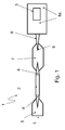
- Figure 1 is an exemplary schematic representation of a top view of a device 1 comprising a BH-SOA 2 and photodetector 3 monolithically integrated according to some embodiments.
- the device 1 is configured to receive input light L through a first spot size converter (SSC) 4 in order to allow efficient and low loss coupling of light between an incoming optical fiber (not shown in the figure) and the BH-SOA 2.
- SSC spot size converter
- a first low confinement optical passive waveguide 5 is preferably used in order to inject the incoming light into the SSC 4.
- Some preferred materials to be used for making a SSC are InGaAsP and InGaAs.
- the SSC 4 thus couples the incoming light into the BH-SOA 2 where it is amplified and is subsequently provided from an active waveguide of the BH-SOA 2 to an output of BH-SOA where it is input in a second SSC 6.
- the second SSC 6 also allows for an efficient and low loss coupling of the light to the next stage of the device 1 which may be a second optical passive waveguide 7.
- the second SSC 6 may have the same structure and be made of the same materials as the first SSC 4.
- the first optical passive waveguide 5 and the second optical passive waveguide 7 may be parts of one and the same structure as shown in figure 2 .
- the light may then be input from the optical passive SOA waveguide 7 into an optical passive transition waveguide 8 preferably made of InGaAsP layer (with the photoluminescence Q of the material being about 1.3 ⁇ m).
- the optical passive transition waveguide 8 may be used to evanescently couple the light to an active region of the photodiode 3.
- Evanescent coupling within the context of the present invention may be produced when an absorbing layer is not in front of the incoming light but displaces, for example on the top of the waveguide which guides the light. As a result the absorption of light is distributed throughout a wider area of absorption, thus the light is evanescently absorbed by the photodiode. This effect may avoid or reduce undesired concentration of photo-generated carriers.
- Figure 2 is an exemplary schematic representation of a cross-sectional view of the device of figure 1 .
- like elements have been given like reference numerals as those of figure1 unless otherwise provided.
- the device 1 comprises a BH-SOA 2 and photodetector 3 monolithically integrated according to some embodiments.
- the photodetector is preferably deep ridge.
- An incoming input light L is preferably input in the optical passive SOA waveguide 5 which is used in order to inject the incoming light L into the first SSC 4.
- the first SSC 4 couples the light to the BH-SOA 2.
- the BH-SOA 2 amplifies the received light and subsequently provides the light at an output thereof where it is input in a second SSC 6.
- the light travelling in, through and out of the BH-SOA has been shown in figure 2 by reference numeral L1.
- the second SSC 6 allows for an efficient and low loss coupling of the light, shown as L2, to the second optical passive SOA waveguide 7.
- the light may then be input from the optical passive SOA waveguide 7 into an optical passive transition waveguide 8 as shown by means of arrows L3.
- the optical passive transition waveguide 8 may be used to evanescently couple the light, shown as L4, to an active region of the photodiode 3.
- the active waveguide of the semiconductor optical amplifier 21 is coupled by means of the second spot size converter 6 to the second optical passive waveguide 7 and the second optical passive waveguide is coupled by means of a third spot size converter 9 to the passive transition waveguide 8.
- This arrangement has the advantage of preventing or substantially reducing backward reflection from the passive transition waveguide 8 toward the semiconductor optical amplifier 2.
- the passive transition waveguide 8 has a planar shape in the vicinity of the photodetector area. This area is schematically shown in figures 1 and 2 by reference numeral 8a.
- the planar shape of the passive transition waveguide is advantageous because it simplifies manufacturing processes.
- Figure 3 is an exemplary graphical illustration of a simulation result related to coupling efficiency between the low confinement passive waveguide and the photodetector (in this case a photodiode) showing a photodiode quantum efficiency versus diode length for a specific diode width and for a specific BH-SOA photodiode optical transition waveguide length.
- the photodetector in this case a photodiode
- this graph is provided merely for the purpose of illustration and better understanding of the embodiments described here.
- this figure shows simulation results it is not to be construed as imposing any limitation on such embodiments.
- the graph of figure 3 relates to a photodiode width of about 4 ⁇ m and for a BH-SOA photodiode optical transition waveguide 8 length (namely from the output of the BH-SOA to the input of the photodiode) with a value greater than zero (>0).
- Said length is represented in figure 2 by reference D for which some preferred values are about 0.1 ⁇ m and about 10 ⁇ m.
- a photodiode of 4x15 ⁇ m 2 (which may be a typical diode area used for 100Gb/s applications) a quantum efficiency of about 42% is achieved - which is considered to be high - at a wavelength of about 1.55 ⁇ m with TE/TM polarization dependence loss of less than about 0.5dB.
- a high gain for example above 20dB
- a high sensitivity for example above 20dB
- the above embodiments are provided for a device structure in which the BH-SOA and the photodetector are provided with certain separation between each other.
- the BH-SOA and PD may be located on approximately or substantially next with respect to each other. This configuration may also be called a butt-coupled configuration.
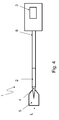
- Figure 4 is an exemplary top view of such a BH-SOA 2 and a deep ridge photodiode 3 monolithically integrated in but-coupled configuration according to some embodiments.
- like elements have been given like reference numbers as those of figures 1 and 2 .
- Butt-coupling is a known technique which presents certain advantages for a number of applications, in particular in case where it is desired to design a device capable of integrating a variety of functionalities, for example multiplexing/demultiplexing in addition to photo-detection.
- the device 1 is configured to receive the input light L through a first spot size converter (SSC) 4 in order to allow efficient and low loss coupling of light between on incoming optical fiber (not shown on the figure) and the BH-SOA 2.
- An optical passive waveguide 5 is preferably used in order to inject the light into a spot size converter (SSC) 4.
- the SSC 4 thus couples the incoming light into the BH-SOA 2 where it is amplified and is subsequently provided at an output of the BH-SOA 2where it is input in the passive transition waveguide 8 preferably made of InGaAsP.
- the optical passive transition waveguide 8 may be used to evanescently couple the light to an active region of the photodiode, as already described in relation to figures 1 and 2 .
- Figure 5 is an exemplary schematic representation of a cross-sectional view of the device of figure 4 .
- the device comprises a BH-SOA 2 and a deep ridge photodiode 3 monolithically integrated according to some embodiments.
- An incoming input light L is preferably input in the optical passive waveguide 5 which is used in order to inject the incoming light L into the first SSC 4 as shown by arrow L1.
- the first SSC 4 couples the light into the BH-SOA 2.
- the BH-SOA 2 amplifies the received light and subsequently provides the light at an output thereof where it is input in the passive transition waveguide 8.
- the light travelling in and through the BH-SOA has been shown in figure 5 by reference numeral L2 and the light travelling in the passive transition waveguide has been shown as L3.
- the optical passive transition waveguide 8 may be used to evanescently couple the light, shown as L4, to an active region of the photodiode 3.
- the length D of the optical transition waveguide 8 (namely from the output of the BH-SOA to the input of the photodiode) may also have any value greater than zero (>0) from which some preferred values are below about 100 ⁇ m, or about 10 ⁇ m.
- the solution proposed herein is related to providing optical pre-amplification which is an important feature for receivers developed for high speed applications (100Gb/s and beyond) with extended transmission reach.
- the integration of an optimized structure of a photodetector (deep ridge compatible for high speed operation) with a buried heterostructure SOA (providing high optical gain, low noise factor and low polarization dependence) preferably taking advantage of an evanescent optical coupling via SSCs and a buried waveguide provides such desired functionalities.
- Such integration scheme is different from the known solutions and may solve the limitation of optical reflection between said two components, which may allow to etch the re-growth interface between the SOA active waveguide and the high confinement passive waveguide which otherwise may cause reflections if the two waveguide are not substantially or perfectly aligned.
- the solution proposed herein provides the advantage of allowing the achievement of high optical gain, low insertion loss and low noise figure. Furthermore, the proposed solution may provide low TE/TM polarization loss and high speed operation as compared to known solutions.
Landscapes
- Physics & Mathematics (AREA)
- General Physics & Mathematics (AREA)
- Optics & Photonics (AREA)
- Condensed Matter Physics & Semiconductors (AREA)
- Electromagnetism (AREA)
- Engineering & Computer Science (AREA)
- Microelectronics & Electronic Packaging (AREA)
- Light Receiving Elements (AREA)
- Optical Integrated Circuits (AREA)
- Semiconductor Lasers (AREA)
- Solid State Image Pick-Up Elements (AREA)
Abstract
Description
- The present invention relates to optical components.
- Optical pre-amplification is widely used for example to increase photoreceivers sensitivity in order to improve the distance for data transmission over optical fiber in digital communication systems. In such systems cost is typically an important issue to be considered. In this regard, monolithic integration of a semiconductor optical amplifier (hereinafter also referred to as SOA) and a photodetector in one InP single chip become particularly important as it may contribute to reducing cost of the receiver terminal as well as its size.
- Before describing the embodiments of the invention, a brief introduction of known solutions is provided.
- Three solutions are known to be used for monolithic integration of SOAs and photodetectors:
- A first solution uses a shallow ridge SOA integrated with a deep ridge photodiode (PD) coupled vertically by lateral taper that allows for a fabrication process with a single step growth of the vertical epitaxial structures of SOA and PD, respectively. However, in such known solution, the coupling between the SOA and the photodiode typically induces propagation losses which typically causes a limitation in the amplification gain (typically less than 10dB). In addition, a low confinement SOA active region is typically required for vertical coupling which typically induces very large TE/TM polarization loss.
- A second known solution relates to employing a similar active region and semiinsulating buried heterostructure for both the SOA and the photodetector (also known as butt-coupling) to increase coupling efficiency between the two optical components. Based on this know solution a larger gain, of about 14dB, has been demonstrated. However, one typical yet important limitation of this known solution is associated to a reduced power saturation of the photodiode due to direct optical injection which typically induces a photodiode bandwidth roll-off about 3-dB. A further drawback is the difficulty (or in occasions impossibility) to optimize independently the thickness of the active region of the SOA and the photodiode, typically leading to poor SOA performances and/or bandwidth limitation of the photodiode.
- A third known solution relates to the use of Quantum Well Intermixing to typically use the same waveguide for the SOA section and the passive section and a photodiode evanescently coupled on top of the passive waveguide. In such solution, the SOA, the passive waveguide and the photodiode typically use the same shallow ridge structure. Although this solution typically allows for evanescent coupling to increase the power saturation of the photodetector and that the common shallow ridge structure simplifies the process of the component, it typically has the drawback of providing such increase of power saturation at the expense of a low coupling efficiency at the SOA input (fiber coupling section) which typically increases the SOA noise figure and therefore typically reduces the sensitivity of the receiver. Spot size converters (SSC) may be a remedy for such coupling problem, however SSCs are typically difficult to achieve with ridge SOA structure because of the high confinement in the active region. A further typical drawback of the shallow ridge structure is the increase of the capacity and the resistance of the photodiode, typically leading to an estimated bandwidth lower than 36 GHz despite a small size (about 90 µm2) and a 25Ω effective load.
- In addition, to the knowledge of the inventors, with this solution only TE mode operating devices have been demonstrated so far.
- Accordingly some embodiments of the invention feature a monolithic integrated structure comprising a buried heterostructure semiconductor optical amplifier comprising an active waveguide and a deep ridge photodetector.
- According to some specific embodiments, the structure comprises a first low confinement optical passive waveguide configured to inject an incoming light into the structure.
- According to some specific embodiments, the structure comprises a first spot size converter configured to allow coupling between the first optical passive waveguide and an active waveguide of the semiconductor optical amplifier. According to some specific embodiments, the structure comprises an optical passive transition waveguide having a high confinement and configured to evanescently couple the light to an active region of the photodiode.
- According to some specific embodiments, the high transition optical passive waveguide comprises an InGaAsP layer.
- According to some specific embodiments, the active waveguide of the semiconductor optical amplifier and the transition optical passive waveguide are butt-coupled.
- According to some specific embodiments, the active waveguide of the semiconductor optical amplifier is coupled by means of a second spot size converter to a second optical passive waveguide and the second optical passive waveguide is coupled by means of a third spot size converter to the passive transition waveguide thereby preventing or substantially reducing backward reflection toward the semiconductor optical amplifier.
- According to some specific embodiment, the passive transition waveguide is planar, at least in part, in the vicinity of the photodetector.
- Some embodiments of the invention feature a receiver comprising the monolithic integrated structure as proposed herein.
- These and further features and advantages of the present invention are described in more detail, for the purpose of illustration and not limitation, in the following description as well as in the claims with the aid of the accompanying drawings.
-
-
Figure 1 is an exemplary schematic representation of a top view of a monolithically integrated buried heterostructure SOA and a deep ridge photodetector according to some embodiments. -
Figure 2 is an exemplary schematic representation of a cross-sectional view of the monolithically integrated buried heterostructure SOA and photodetector offigure 1 . -
Figure 3 is an exemplary graphical illustration of a simulation result related to a coupling efficiency between a and an SOA wherein photodiode quantum efficiency is shown versus diode length for a specific diode width and for a specific BH-SOA photodiode optical transition waveguide length. -
Figure 4 is an exemplary schematic representation of a top view of a monolithically integrated BH-SOA and a deep ridge photodetector in but-coupled configuration according to some embodiments. -
Figure 5 is an exemplary schematic representation of a cross-sectional view of the monolithically integrated buried heterostructure SOA and photodetector offigure 4 . - Embodiments of the invention relate to the use of a buried heterostructure SOA monolithically integrated with a photodiode.
- A buried heterostructure (BH) configuration is known in the related art. In brief, such configuration comprises various layers or regions of semiconductor material with different crystalline structures which in turn gives rise to different band-gaps within the structure.
- A buried heterostructure is preferred to be used in an SOA because it may allow a better thermal dissipation and lower optical losses than shallow ridge and deep ridge structures. Furthermore, it may become comparatively easier to obtain low polarization dependence together with low coupling loss with optical fiber when use is made of a buried heterostructure rather than of shallow ridge and deep ridge structures.
- Some preferred materials to be used for making a BH-SOA are InGaAsP and InGaAs.
- The photodiode structure is provided in deep ridge configuration which is compatible with high speed operation (low junction capacitance and low resistance).
- Some preferred materials to be used for making a Photodetector are InGaAsP, InGaAs and InP.
- In order to ensure high coupling efficiency and electrical isolation between the SOA and the photodetector a high confinement passive transition optical waveguide may be inserted between the SOA output passive optical waveguide and the photodetector.
- In the context of the present description, reference to "high" confinement waveguide is to be understood to relate to an optical waveguide which is capable of carrying an optical mode with an area typically having a width at 1/e2 of about 1.5µm or less and a high optical confinement in the waveguide layer (for example about 60%). Similarly, a low confinement optical waveguide is a waveguide which is capable of carrying an optical mode with an area typically having a width at 1/e2 between about 1.5µm and 6 µm and a low optical confinement in the waveguide layer (for example about 15%). By way of illustrative and non-limiting example it is to be noted that a low confinement waveguide may be made in InGaAsP material (photoluminescence of about 1.17 µm) having a thickness of about 0.15 µm and a width of about 3 µm; similarly, a high confinement waveguide may be made in InGaAsP material (photoluminescence of about 1.3 µm) having a of thickness of about 0.52 µm and a width of about 0.13 to 3µm and about 1.1 µm in butt coupled configuration.
- Such passive waveguide may provide electrical isolation and the high confinement characteristic of the waveguide may greatly improve coupling efficiency and reduce reflection in the BH structure and the planar section area. This solution has also the advantage of reducing reflection between the BH structure and the planar section where the photodetector is provided as will be described in further detail below.
- A preferred material to be used for making a passive transition waveguide is InGaAsP.
-
Figure 1 is an exemplary schematic representation of a top view of adevice 1 comprising a BH-SOA 2 andphotodetector 3 monolithically integrated according to some embodiments. Thedevice 1 is configured to receive input light L through a first spot size converter (SSC) 4 in order to allow efficient and low loss coupling of light between an incoming optical fiber (not shown in the figure) and the BH-SOA 2. A first low confinement opticalpassive waveguide 5 is preferably used in order to inject the incoming light into theSSC 4. - Some preferred materials to be used for making a SSC are InGaAsP and InGaAs.
- The
SSC 4 thus couples the incoming light into the BH-SOA 2 where it is amplified and is subsequently provided from an active waveguide of the BH-SOA 2 to an output of BH-SOA where it is input in asecond SSC 6. Thesecond SSC 6 also allows for an efficient and low loss coupling of the light to the next stage of thedevice 1 which may be a second opticalpassive waveguide 7. Thesecond SSC 6 may have the same structure and be made of the same materials as thefirst SSC 4. Furthermore the first opticalpassive waveguide 5 and the second opticalpassive waveguide 7 may be parts of one and the same structure as shown infigure 2 . - The light may then be input from the optical
passive SOA waveguide 7 into an opticalpassive transition waveguide 8 preferably made of InGaAsP layer (with the photoluminescence Q of the material being about 1.3µm). The opticalpassive transition waveguide 8 may be used to evanescently couple the light to an active region of thephotodiode 3. - Evanescent coupling within the context of the present invention may be produced when an absorbing layer is not in front of the incoming light but displaces, for example on the top of the waveguide which guides the light. As a result the absorption of light is distributed throughout a wider area of absorption, thus the light is evanescently absorbed by the photodiode. This effect may avoid or reduce undesired concentration of photo-generated carriers.
-
Figure 2 is an exemplary schematic representation of a cross-sectional view of the device offigure 1 . In this figure like elements have been given like reference numerals as those offigure1 unless otherwise provided. - As shown in
figure 2 , thedevice 1 comprises a BH-SOA 2 andphotodetector 3 monolithically integrated according to some embodiments. The photodetector is preferably deep ridge. - An incoming input light L is preferably input in the optical
passive SOA waveguide 5 which is used in order to inject the incoming light L into thefirst SSC 4. Thefirst SSC 4 couples the light to the BH-SOA 2. - As already mentioned above the BH-
SOA 2 amplifies the received light and subsequently provides the light at an output thereof where it is input in asecond SSC 6. The light travelling in, through and out of the BH-SOA has been shown infigure 2 by reference numeral L1. Thesecond SSC 6 allows for an efficient and low loss coupling of the light, shown as L2, to the second opticalpassive SOA waveguide 7. The light may then be input from the opticalpassive SOA waveguide 7 into an opticalpassive transition waveguide 8 as shown by means of arrows L3. The opticalpassive transition waveguide 8 may be used to evanescently couple the light, shown as L4, to an active region of thephotodiode 3. - As shown more clearly in
figure 1 , the active waveguide of the semiconductor optical amplifier 21 is coupled by means of the secondspot size converter 6 to the second opticalpassive waveguide 7 and the second optical passive waveguide is coupled by means of a thirdspot size converter 9 to thepassive transition waveguide 8. This arrangement has the advantage of preventing or substantially reducing backward reflection from thepassive transition waveguide 8 toward the semiconductoroptical amplifier 2. - Preferably, the
passive transition waveguide 8 has a planar shape in the vicinity of the photodetector area. This area is schematically shown infigures 1 and2 byreference numeral 8a. The planar shape of the passive transition waveguide is advantageous because it simplifies manufacturing processes. -
Figure 3 is an exemplary graphical illustration of a simulation result related to coupling efficiency between the low confinement passive waveguide and the photodetector (in this case a photodiode) showing a photodiode quantum efficiency versus diode length for a specific diode width and for a specific BH-SOA photodiode optical transition waveguide length. It is to be noted that this graph is provided merely for the purpose of illustration and better understanding of the embodiments described here. Thus, although this figure shows simulation results it is not to be construed as imposing any limitation on such embodiments. The graph offigure 3 relates to a photodiode width of about 4µm and for a BH-SOA photodiodeoptical transition waveguide 8 length (namely from the output of the BH-SOA to the input of the photodiode) with a value greater than zero (>0). Said length is represented infigure 2 by reference D for which some preferred values are about 0.1 µm and about 10µm. For a photodiode of 4x15µm2 (which may be a typical diode area used for 100Gb/s applications) a quantum efficiency of about 42% is achieved - which is considered to be high - at a wavelength of about 1.55µm with TE/TM polarization dependence loss of less than about 0.5dB. When using SOA optical pre-amplification, a high gain (for example above 20dB) is expected allowing high sensitivity. - The above embodiments are provided for a device structure in which the BH-SOA and the photodetector are provided with certain separation between each other. According to alternative embodiments the BH-SOA and PD may be located on approximately or substantially next with respect to each other. This configuration may also be called a butt-coupled configuration.
-
Figure 4 is an exemplary top view of such a BH-SOA 2 and adeep ridge photodiode 3 monolithically integrated in but-coupled configuration according to some embodiments. In this figure, like elements have been given like reference numbers as those offigures 1 and2 . - Butt-coupling is a known technique which presents certain advantages for a number of applications, in particular in case where it is desired to design a device capable of integrating a variety of functionalities, for example multiplexing/demultiplexing in addition to photo-detection.
- Referring back to
figure 4 , thedevice 1 is configured to receive the input light L through a first spot size converter (SSC) 4 in order to allow efficient and low loss coupling of light between on incoming optical fiber (not shown on the figure) and the BH-SOA 2. An opticalpassive waveguide 5 is preferably used in order to inject the light into a spot size converter (SSC) 4. - The
SSC 4 thus couples the incoming light into the BH-SOA 2 where it is amplified and is subsequently provided at an output of the BH-SOA 2where it is input in thepassive transition waveguide 8 preferably made of InGaAsP. The opticalpassive transition waveguide 8 may be used to evanescently couple the light to an active region of the photodiode, as already described in relation tofigures 1 and2 . -
Figure 5 is an exemplary schematic representation of a cross-sectional view of the device offigure 4 . - As shown in
figure 5 , the device comprises a BH-SOA 2 and adeep ridge photodiode 3 monolithically integrated according to some embodiments. - An incoming input light L is preferably input in the optical
passive waveguide 5 which is used in order to inject the incoming light L into thefirst SSC 4 as shown by arrow L1. Thefirst SSC 4 couples the light into the BH-SOA 2. - As already mentioned above, the BH-
SOA 2 amplifies the received light and subsequently provides the light at an output thereof where it is input in thepassive transition waveguide 8. The light travelling in and through the BH-SOA has been shown infigure 5 by reference numeral L2 and the light travelling in the passive transition waveguide has been shown as L3. The opticalpassive transition waveguide 8 may be used to evanescently couple the light, shown as L4, to an active region of thephotodiode 3. - In the butt-coupled configuration of
figures 4 and5 , the length D of the optical transition waveguide 8 (namely from the output of the BH-SOA to the input of the photodiode) may also have any value greater than zero (>0) from which some preferred values are below about 100µm, or about 10µm. - The solution proposed herein is related to providing optical pre-amplification which is an important feature for receivers developed for high speed applications (100Gb/s and beyond) with extended transmission reach. The integration of an optimized structure of a photodetector (deep ridge compatible for high speed operation) with a buried heterostructure SOA (providing high optical gain, low noise factor and low polarization dependence) preferably taking advantage of an evanescent optical coupling via SSCs and a buried waveguide provides such desired functionalities. Such integration scheme is different from the known solutions and may solve the limitation of optical reflection between said two components, which may allow to etch the re-growth interface between the SOA active waveguide and the high confinement passive waveguide which otherwise may cause reflections if the two waveguide are not substantially or perfectly aligned.
- Thus the solution proposed herein provides the advantage of allowing the achievement of high optical gain, low insertion loss and low noise figure. Furthermore, the proposed solution may provide low TE/TM polarization loss and high speed operation as compared to known solutions.
- Further it is to be noted that the list of structures corresponding to the claimed means is not exhaustive and that one skilled in the art understands that equivalent structures can be substituted for the recited structure without departing from the scope of the invention.
- It should be appreciated by those skilled in the art that any block diagrams herein represent conceptual views of illustrative circuitry embodying the principles of the invention.
Claims (9)
- A monolithic integrated structure comprising a buried heterostructure semiconductor optical amplifier comprising an active waveguide and a deep ridge photodetector.
- The structure of claim 1 comprising a first low confinement optical passive waveguide configured to inject an incoming light into the structure.
- The structure of claim 2 comprising a first spot size converter configured to allow coupling between the first optical passive waveguide and the active waveguide of the semiconductor optical amplifier.
- The structure of any one of claims 1 to 3 comprising an optical passive transition waveguide having a high confinement and configured to evanescently couple the light to an active region of the photodiode.
- The structure of claim 4 wherein the high transition optical passive waveguide comprises an InGaAsP layer.
- The structure of any one of claims 1 to 5 wherein the active waveguide of the semiconductor optical amplifier and the transition optical passive waveguide are butt-coupled.
- The structure of any one of claims 1 to 5 wherein the active waveguide of the semiconductor optical amplifier is coupled by means of a second spot size converter to a second optical passive waveguide and the second optical passive waveguide is coupled by means of a third spot size converter to the passive transition waveguide thereby preventing or substantially reducing backward reflection toward the semiconductor optical amplifier.
- The structure of any one of claims 1 to 7 wherein the passive transition waveguide is planar, at least in part, in the vicinity of the photodetector.
- A receiver comprising the monolithic integrated structure of any one of claim 1 to 8.
Priority Applications (7)
| Application Number | Priority Date | Filing Date | Title |
|---|---|---|---|
| EP10306064A EP2439822A1 (en) | 2010-09-30 | 2010-09-30 | A monolithic integrated structure comprising a buried heterostructure semiconductor optical amplifier and a photodetector |
| KR1020137011120A KR101525334B1 (en) | 2010-09-30 | 2011-09-27 | A monolithic integrated structure comprising a buried heterostructure semiconductor optical amplifier and a photodetector |
| CN201180047519.XA CN103154791B (en) | 2010-09-30 | 2011-09-27 | Monolithically Integrated Structures Containing Buried Heterostructure Semiconductor Optical Amplifiers and Photodetectors |
| JP2013530701A JP5837601B2 (en) | 2010-09-30 | 2011-09-27 | Monolithic integrated structure with buried heterostructure semiconductor optical amplifier and photodetector |
| PCT/EP2011/066766 WO2012041850A1 (en) | 2010-09-30 | 2011-09-27 | A monolithic integrated structure comprising a buried heterostructure semiconductor optical amplifier and a photodetector |
| US13/824,726 US8995804B2 (en) | 2010-09-30 | 2011-09-27 | Monolithic integrated structure comprising a buried heterostructure semiconductor optical amplifier and a photodetector |
| SG2013022223A SG189094A1 (en) | 2010-09-30 | 2011-09-27 | A monolithic integrated structure comprising a buried heterostructure semiconductor optical amplifier and a photodetector |
Applications Claiming Priority (1)
| Application Number | Priority Date | Filing Date | Title |
|---|---|---|---|
| EP10306064A EP2439822A1 (en) | 2010-09-30 | 2010-09-30 | A monolithic integrated structure comprising a buried heterostructure semiconductor optical amplifier and a photodetector |
Publications (1)
| Publication Number | Publication Date |
|---|---|
| EP2439822A1 true EP2439822A1 (en) | 2012-04-11 |
Family
ID=43446382
Family Applications (1)
| Application Number | Title | Priority Date | Filing Date |
|---|---|---|---|
| EP10306064A Withdrawn EP2439822A1 (en) | 2010-09-30 | 2010-09-30 | A monolithic integrated structure comprising a buried heterostructure semiconductor optical amplifier and a photodetector |
Country Status (7)
| Country | Link |
|---|---|
| US (1) | US8995804B2 (en) |
| EP (1) | EP2439822A1 (en) |
| JP (1) | JP5837601B2 (en) |
| KR (1) | KR101525334B1 (en) |
| CN (1) | CN103154791B (en) |
| SG (1) | SG189094A1 (en) |
| WO (1) | WO2012041850A1 (en) |
Cited By (5)
| Publication number | Priority date | Publication date | Assignee | Title |
|---|---|---|---|---|
| EP2730958A1 (en) * | 2012-11-07 | 2014-05-14 | Alcatel-Lucent | Amplified coherent detector |
| EP2924481A1 (en) * | 2014-03-26 | 2015-09-30 | Alcatel Lucent | Monolithically integrated photonic tunable receiver for selecting optical signals with different wavelengths |
| CN111801610A (en) * | 2018-02-19 | 2020-10-20 | 三菱电机株式会社 | Semiconductor Optical Integrated Devices |
| EP3153899B1 (en) * | 2015-10-09 | 2024-07-31 | Huawei Technologies Research & Development Belgium NV | Optical coupling scheme |
| DE112014004392B4 (en) | 2013-10-31 | 2025-01-23 | International Business Machines Corporation | Photonic circuit unit with on-chip measurement structures for optical amplification |
Families Citing this family (13)
| Publication number | Priority date | Publication date | Assignee | Title |
|---|---|---|---|---|
| JP2013197200A (en) * | 2012-03-16 | 2013-09-30 | Sumitomo Electric Device Innovations Inc | Photoreceiver control method and communication control method |
| EP3051692A1 (en) * | 2015-01-30 | 2016-08-03 | Alcatel Lucent | Optical device with semiconductor optical amplifier with automatic current supply control |
| US11262605B2 (en) * | 2017-08-31 | 2022-03-01 | Lightwave Logic Inc. | Active region-less polymer modulator integrated on a common PIC platform and method |
| US10340661B2 (en) * | 2017-11-01 | 2019-07-02 | International Business Machines Corporation | Electro-optical device with lateral current injection regions |
| KR102553852B1 (en) * | 2017-11-10 | 2023-07-13 | 한국전자통신연구원 | optical coupling device and manufacturing method of the same |
| JP7247120B2 (en) * | 2018-02-08 | 2023-03-28 | 古河電気工業株式会社 | Optical integrated device and optical module |
| EP3821505A4 (en) * | 2018-07-13 | 2022-07-06 | The Government of the United States of America as represented by the Secretary of the Navy | HIGHLY STABLE SEMICONDUCTOR SENSORS AND LASERS FOR PHOTONIC INTEGRATED CIRCUITS ON III-V AND ON SILICON |
| CN109585610B (en) * | 2018-12-29 | 2024-10-01 | 华进半导体封装先导技术研发中心有限公司 | Butt-coupled detector and method for manufacturing same |
| US10718898B1 (en) * | 2019-01-23 | 2020-07-21 | Nexus Photonics Llc | Integrated active devices with improved optical coupling to dielectric waveguides |
| JP7218652B2 (en) * | 2019-03-28 | 2023-02-07 | 住友大阪セメント株式会社 | light control element |
| US12300966B2 (en) | 2019-09-17 | 2025-05-13 | Mitsubishi Electric Corporation | Semiconductor laser device |
| CN114171613A (en) * | 2021-12-06 | 2022-03-11 | 苏州旭创科技有限公司 | Photoelectric detector |
| US20250035849A1 (en) * | 2023-07-26 | 2025-01-30 | Ali Eshaghian Dorche | Heterogeneously integrated photonic platform supporting large effective mode area waveguides and thermally optimized active components |
Citations (5)
| Publication number | Priority date | Publication date | Assignee | Title |
|---|---|---|---|---|
| EP0469793A2 (en) * | 1990-08-03 | 1992-02-05 | AT&T Corp. | Monolithic integrated optical amplifier and photodetector |
| WO2003102659A2 (en) * | 2001-10-09 | 2003-12-11 | Infinera Corporation | Demultiplexing optical signal receiver photonic integrated circuit (rxpic) and associated transmitter and method of testing a photonic integrated circuit |
| WO2003102678A1 (en) * | 2002-06-04 | 2003-12-11 | The Trustees Of Princeton University | Photonic integrated circuits |
| US20070092192A1 (en) * | 2005-08-05 | 2007-04-26 | Mohand Achouche | Integrated optoelectronic device including a semiconductor optical amplifier and a photodiode |
| US20070110357A1 (en) * | 2005-11-15 | 2007-05-17 | Forrest Stephen R | Integrated photonic amplifier and detector |
Family Cites Families (6)
| Publication number | Priority date | Publication date | Assignee | Title |
|---|---|---|---|---|
| US6330378B1 (en) * | 2000-05-12 | 2001-12-11 | The Trustees Of Princeton University | Photonic integrated detector having a plurality of asymmetric waveguides |
| KR100617693B1 (en) | 2003-08-20 | 2006-08-28 | 삼성전자주식회사 | Semiconductor optical amplifier with photodetector and manufacturing method thereof |
| KR100520796B1 (en) | 2003-10-20 | 2005-10-13 | 한국전자통신연구원 | Method for manufacturing semiconductor optical amplifier having planar buried heteostructure |
| KR100759805B1 (en) * | 2005-12-07 | 2007-09-20 | 한국전자통신연구원 | Optically boosted elctroabsorption duplexer |
| US7738167B2 (en) * | 2005-12-09 | 2010-06-15 | Electronics And Telecommunications Research Institute | Reflective semiconductor optical amplifier (RSOA), RSOA module having the same, and passive optical network using the same |
| US20100111468A1 (en) * | 2007-03-30 | 2010-05-06 | The Furukawa Electric Co., Ltd. | Optical integrated circuit and optical integrated circuit module |
-
2010
- 2010-09-30 EP EP10306064A patent/EP2439822A1/en not_active Withdrawn
-
2011
- 2011-09-27 CN CN201180047519.XA patent/CN103154791B/en not_active Expired - Fee Related
- 2011-09-27 WO PCT/EP2011/066766 patent/WO2012041850A1/en not_active Ceased
- 2011-09-27 JP JP2013530701A patent/JP5837601B2/en not_active Expired - Fee Related
- 2011-09-27 KR KR1020137011120A patent/KR101525334B1/en not_active Expired - Fee Related
- 2011-09-27 US US13/824,726 patent/US8995804B2/en active Active
- 2011-09-27 SG SG2013022223A patent/SG189094A1/en unknown
Patent Citations (5)
| Publication number | Priority date | Publication date | Assignee | Title |
|---|---|---|---|---|
| EP0469793A2 (en) * | 1990-08-03 | 1992-02-05 | AT&T Corp. | Monolithic integrated optical amplifier and photodetector |
| WO2003102659A2 (en) * | 2001-10-09 | 2003-12-11 | Infinera Corporation | Demultiplexing optical signal receiver photonic integrated circuit (rxpic) and associated transmitter and method of testing a photonic integrated circuit |
| WO2003102678A1 (en) * | 2002-06-04 | 2003-12-11 | The Trustees Of Princeton University | Photonic integrated circuits |
| US20070092192A1 (en) * | 2005-08-05 | 2007-04-26 | Mohand Achouche | Integrated optoelectronic device including a semiconductor optical amplifier and a photodiode |
| US20070110357A1 (en) * | 2005-11-15 | 2007-05-17 | Forrest Stephen R | Integrated photonic amplifier and detector |
Non-Patent Citations (2)
| Title |
|---|
| MASON B ET AL: "Photonic integrated receiver for 40 Gbit/s transmission", ELECTRONICS LETTERS, IEE STEVENAGE, GB, vol. 38, no. 20, 26 September 2002 (2002-09-26), pages 1196 - 1197, XP006018867, ISSN: 0013-5194, DOI: 10.1049/EL:20020778 * |
| SU HWAN OH ET AL.: "Fabrication of transmit-receive devices monolithically integrated with semiconductor optical amplifier", JAPANESE JOURNAL OF APPLIED PHYSICS, PART 1 (REGULAR PAPERS, SHORT NOTES & REVIEW PAPERS) JAPAN SOCIETY OF APPLIED PHYSICS THROUGH THE INSTITUTE OF PURE AND APPLIED PHYSICS JAPAN, vol. 47, no. 5, 16 May 2008 (2008-05-16), pages 3489 - 3492, XP002618197, ISSN: 0021-4922, DOI: 10.1143/JJAP.47.3489 * |
Cited By (5)
| Publication number | Priority date | Publication date | Assignee | Title |
|---|---|---|---|---|
| EP2730958A1 (en) * | 2012-11-07 | 2014-05-14 | Alcatel-Lucent | Amplified coherent detector |
| DE112014004392B4 (en) | 2013-10-31 | 2025-01-23 | International Business Machines Corporation | Photonic circuit unit with on-chip measurement structures for optical amplification |
| EP2924481A1 (en) * | 2014-03-26 | 2015-09-30 | Alcatel Lucent | Monolithically integrated photonic tunable receiver for selecting optical signals with different wavelengths |
| EP3153899B1 (en) * | 2015-10-09 | 2024-07-31 | Huawei Technologies Research & Development Belgium NV | Optical coupling scheme |
| CN111801610A (en) * | 2018-02-19 | 2020-10-20 | 三菱电机株式会社 | Semiconductor Optical Integrated Devices |
Also Published As
| Publication number | Publication date |
|---|---|
| KR20130093636A (en) | 2013-08-22 |
| JP5837601B2 (en) | 2015-12-24 |
| US20130301985A1 (en) | 2013-11-14 |
| CN103154791B (en) | 2015-07-01 |
| JP2013540351A (en) | 2013-10-31 |
| SG189094A1 (en) | 2013-05-31 |
| US8995804B2 (en) | 2015-03-31 |
| WO2012041850A1 (en) | 2012-04-05 |
| CN103154791A (en) | 2013-06-12 |
| KR101525334B1 (en) | 2015-06-02 |
Similar Documents
| Publication | Publication Date | Title |
|---|---|---|
| US8995804B2 (en) | Monolithic integrated structure comprising a buried heterostructure semiconductor optical amplifier and a photodetector | |
| Kato et al. | Design of ultrawide-band, high-sensitivity pin protodetectors | |
| Beling et al. | High-speed photodiodes | |
| US7851782B2 (en) | Photodetector including multiple waveguides | |
| US20090245298A1 (en) | Hybrid silicon laser-quantum well intermixing wafer bonded integration platform for advanced photonic circuits with electroabsorption modulators | |
| US10680412B2 (en) | Optical coupling connector, optical coupling system, and waveguide coupling method | |
| CA2408768A1 (en) | Photonic integrated detector having a plurality of asymmetric waveguides | |
| CN102713703A (en) | Waveguide optically pre-amplified detector with passband wavelength filtering | |
| Caillaud et al. | Monolithic integration of a semiconductor optical amplifier and a high-speed photodiode with low polarization dependence loss | |
| US10134937B2 (en) | Semiconductor photodiode | |
| Xia et al. | Monolithic integration of a semiconductor optical amplifier and a high bandwidth pin photodiode using asymmetric twin-waveguide technology | |
| Hong et al. | Monolithically integrated waveguide-MSM detector-HEMT amplifier receiver for long-waveguide lightwave systems | |
| CN110383126B (en) | Quantum dot semiconductor optical amplifier and quantum dot photodetector | |
| US11929592B2 (en) | Silicon-photonics-based semiconductor optical amplifier with N-doped active layer | |
| US8224134B2 (en) | Optoelectronic receiver | |
| Tolstikhin et al. | Single-mode vertical integration of PIN photodetectors with optical waveguides for monitoring in WDM transmission systems | |
| TW201246736A (en) | A monolithic integrated structure comprising a buried heterostructure semiconductor optical amplifier and a photodetector | |
| JP2833615B2 (en) | Optical semiconductor integrated device | |
| Kang et al. | Optical coupling analysis of dual-waveguide structure for monolithic integration of photonic devices | |
| JP3757955B2 (en) | Loaded semiconductor photo detector | |
| KR100276082B1 (en) | Structure of bidirectional optical device operating with a single power supply and its manufacturing method | |
| EP4016764A1 (en) | Gain medium structure for semiconductor optical amplifier with high saturation power | |
| Shi et al. | High-speed and high-power InP based photodiode for the applications of microwave photonics | |
| Tauke-Pedretti et al. | Cascaded double ring resonator filter with integrated SOAs | |
| Matsuoka et al. | High-speed optical devices for 40 Gbit/s optical receivers |
Legal Events
| Date | Code | Title | Description |
|---|---|---|---|
| AK | Designated contracting states |
Kind code of ref document: A1 Designated state(s): AL AT BE BG CH CY CZ DE DK EE ES FI FR GB GR HR HU IE IS IT LI LT LU LV MC MK MT NL NO PL PT RO SE SI SK SM TR |
|
| AX | Request for extension of the european patent |
Extension state: BA ME RS |
|
| PUAI | Public reference made under article 153(3) epc to a published international application that has entered the european phase |
Free format text: ORIGINAL CODE: 0009012 |
|
| 17P | Request for examination filed |
Effective date: 20121011 |
|
| 111Z | Information provided on other rights and legal means of execution |
Free format text: AL AT BE BG CH CY CZ DE DK EE ES FI FR GB GR HR HU IE IS IT LI LT LU LV MC MK MT NL NO PL PT RO SE SI SK SM TR Effective date: 20130410 |
|
| RAP1 | Party data changed (applicant data changed or rights of an application transferred) |
Owner name: ALCATEL LUCENT |
|
| D11X | Information provided on other rights and legal means of execution (deleted) | ||
| 17Q | First examination report despatched |
Effective date: 20150121 |
|
| GRAP | Despatch of communication of intention to grant a patent |
Free format text: ORIGINAL CODE: EPIDOSNIGR1 |
|
| RIC1 | Information provided on ipc code assigned before grant |
Ipc: H01S 5/026 20060101AFI20170310BHEP Ipc: H01S 5/50 20060101ALN20170310BHEP Ipc: G02B 6/12 20060101ALN20170310BHEP Ipc: G02B 6/26 20060101ALN20170310BHEP Ipc: H01S 5/227 20060101ALN20170310BHEP Ipc: H04B 10/67 20130101ALI20170310BHEP |
|
| RIC1 | Information provided on ipc code assigned before grant |
Ipc: G02B 6/12 20060101ALN20170321BHEP Ipc: G02B 6/26 20060101ALN20170321BHEP Ipc: H01S 5/227 20060101ALN20170321BHEP Ipc: H01S 5/026 20060101AFI20170321BHEP Ipc: H04B 10/67 20130101ALI20170321BHEP Ipc: H01S 5/50 20060101ALN20170321BHEP |
|
| INTG | Intention to grant announced |
Effective date: 20170407 |
|
| STAA | Information on the status of an ep patent application or granted ep patent |
Free format text: STATUS: THE APPLICATION IS DEEMED TO BE WITHDRAWN |
|
| 18D | Application deemed to be withdrawn |
Effective date: 20170818 |
|
| RIC1 | Information provided on ipc code assigned before grant |
Ipc: H01S 5/50 20060101ALN20170321BHEP Ipc: H04B 10/67 20130101ALI20170321BHEP Ipc: G02B 6/12 20060101ALN20170321BHEP Ipc: G02B 6/26 20060101ALN20170321BHEP Ipc: H01S 5/026 20060101AFI20170321BHEP Ipc: H01S 5/227 20060101ALN20170321BHEP |
|
| RIC1 | Information provided on ipc code assigned before grant |
Ipc: G02B 6/12 20060101ALN20170321BHEP Ipc: G02B 6/26 20060101ALN20170321BHEP Ipc: H01S 5/227 20060101ALN20170321BHEP Ipc: H04B 10/67 20130101ALI20170321BHEP Ipc: H01S 5/50 20060101ALN20170321BHEP Ipc: H01S 5/026 20060101AFI20170321BHEP |